EP0359508A2 - Sequential-quenching resonant-tunneling transistor - Google Patents
Sequential-quenching resonant-tunneling transistor Download PDFInfo
- Publication number
- EP0359508A2 EP0359508A2 EP89309206A EP89309206A EP0359508A2 EP 0359508 A2 EP0359508 A2 EP 0359508A2 EP 89309206 A EP89309206 A EP 89309206A EP 89309206 A EP89309206 A EP 89309206A EP 0359508 A2 EP0359508 A2 EP 0359508A2
- Authority
- EP
- European Patent Office
- Prior art keywords
- circuit
- region
- quantum wells
- emitter
- quantum
- Prior art date
- Legal status (The legal status is an assumption and is not a legal conclusion. Google has not performed a legal analysis and makes no representation as to the accuracy of the status listed.)
- Ceased
Links
- 238000010791 quenching Methods 0.000 title claims description 9
- 230000015654 memory Effects 0.000 claims abstract description 5
- 230000005641 tunneling Effects 0.000 claims description 23
- 239000004065 semiconductor Substances 0.000 claims description 14
- 239000000203 mixture Substances 0.000 claims description 10
- 230000006870 function Effects 0.000 claims description 8
- 230000000171 quenching effect Effects 0.000 claims description 8
- 230000003993 interaction Effects 0.000 claims description 4
- 239000000463 material Substances 0.000 claims description 4
- 238000012545 processing Methods 0.000 claims description 4
- 238000006243 chemical reaction Methods 0.000 claims 1
- 238000010586 diagram Methods 0.000 description 14
- IJGRMHOSHXDMSA-UHFFFAOYSA-N Atomic nitrogen Chemical compound N#N IJGRMHOSHXDMSA-UHFFFAOYSA-N 0.000 description 11
- 229910000530 Gallium indium arsenide Inorganic materials 0.000 description 7
- 229910052757 nitrogen Inorganic materials 0.000 description 6
- 238000012546 transfer Methods 0.000 description 6
- 229910000673 Indium arsenide Inorganic materials 0.000 description 4
- AJGDITRVXRPLBY-UHFFFAOYSA-N aluminum indium Chemical compound [Al].[In] AJGDITRVXRPLBY-UHFFFAOYSA-N 0.000 description 4
- 239000007788 liquid Substances 0.000 description 4
- 230000004888 barrier function Effects 0.000 description 3
- PCHJSUWPFVWCPO-UHFFFAOYSA-N gold Chemical compound [Au] PCHJSUWPFVWCPO-UHFFFAOYSA-N 0.000 description 3
- 229910052737 gold Inorganic materials 0.000 description 3
- 239000010931 gold Substances 0.000 description 3
- GPXJNWSHGFTCBW-UHFFFAOYSA-N Indium phosphide Chemical compound [In]#P GPXJNWSHGFTCBW-UHFFFAOYSA-N 0.000 description 2
- MDPILPRLPQYEEN-UHFFFAOYSA-N aluminium arsenide Chemical compound [As]#[Al] MDPILPRLPQYEEN-UHFFFAOYSA-N 0.000 description 2
- 239000000969 carrier Substances 0.000 description 2
- 239000002019 doping agent Substances 0.000 description 2
- 230000005684 electric field Effects 0.000 description 2
- 238000001704 evaporation Methods 0.000 description 2
- 238000000034 method Methods 0.000 description 2
- 230000003647 oxidation Effects 0.000 description 2
- 238000007254 oxidation reaction Methods 0.000 description 2
- 229910000980 Aluminium gallium arsenide Inorganic materials 0.000 description 1
- JBRZTFJDHDCESZ-UHFFFAOYSA-N AsGa Chemical compound [As]#[Ga] JBRZTFJDHDCESZ-UHFFFAOYSA-N 0.000 description 1
- 229910000952 Be alloy Inorganic materials 0.000 description 1
- 229910001218 Gallium arsenide Inorganic materials 0.000 description 1
- UFHFLCQGNIYNRP-UHFFFAOYSA-N Hydrogen Chemical compound [H][H] UFHFLCQGNIYNRP-UHFFFAOYSA-N 0.000 description 1
- BQCADISMDOOEFD-UHFFFAOYSA-N Silver Chemical compound [Ag] BQCADISMDOOEFD-UHFFFAOYSA-N 0.000 description 1
- KXNLCSXBJCPWGL-UHFFFAOYSA-N [Ga].[As].[In] Chemical compound [Ga].[As].[In] KXNLCSXBJCPWGL-UHFFFAOYSA-N 0.000 description 1
- 238000005229 chemical vapour deposition Methods 0.000 description 1
- 238000005253 cladding Methods 0.000 description 1
- 238000013500 data storage Methods 0.000 description 1
- 230000007423 decrease Effects 0.000 description 1
- 238000011161 development Methods 0.000 description 1
- 238000009792 diffusion process Methods 0.000 description 1
- 238000009826 distribution Methods 0.000 description 1
- 230000005669 field effect Effects 0.000 description 1
- 229910052732 germanium Inorganic materials 0.000 description 1
- GNPVGFCGXDBREM-UHFFFAOYSA-N germanium atom Chemical compound [Ge] GNPVGFCGXDBREM-UHFFFAOYSA-N 0.000 description 1
- 230000005283 ground state Effects 0.000 description 1
- 229910052734 helium Inorganic materials 0.000 description 1
- 239000001307 helium Substances 0.000 description 1
- SWQJXJOGLNCZEY-UHFFFAOYSA-N helium atom Chemical compound [He] SWQJXJOGLNCZEY-UHFFFAOYSA-N 0.000 description 1
- 239000001257 hydrogen Substances 0.000 description 1
- 229910052739 hydrogen Inorganic materials 0.000 description 1
- 238000010348 incorporation Methods 0.000 description 1
- 230000002401 inhibitory effect Effects 0.000 description 1
- 238000002347 injection Methods 0.000 description 1
- 239000007924 injection Substances 0.000 description 1
- 230000010354 integration Effects 0.000 description 1
- 238000001465 metallisation Methods 0.000 description 1
- 238000001451 molecular beam epitaxy Methods 0.000 description 1
- 238000000206 photolithography Methods 0.000 description 1
- 230000008569 process Effects 0.000 description 1
- 238000012216 screening Methods 0.000 description 1
- 238000000926 separation method Methods 0.000 description 1
- 229910052709 silver Inorganic materials 0.000 description 1
- 239000004332 silver Substances 0.000 description 1
- 239000000126 substance Substances 0.000 description 1
- 239000000758 substrate Substances 0.000 description 1
- 238000001039 wet etching Methods 0.000 description 1
Images


Classifications
-
- H—ELECTRICITY
- H01—ELECTRIC ELEMENTS
- H01L—SEMICONDUCTOR DEVICES NOT COVERED BY CLASS H10
- H01L27/00—Devices consisting of a plurality of semiconductor or other solid-state components formed in or on a common substrate
-
- B—PERFORMING OPERATIONS; TRANSPORTING
- B82—NANOTECHNOLOGY
- B82Y—SPECIFIC USES OR APPLICATIONS OF NANOSTRUCTURES; MEASUREMENT OR ANALYSIS OF NANOSTRUCTURES; MANUFACTURE OR TREATMENT OF NANOSTRUCTURES
- B82Y10/00—Nanotechnology for information processing, storage or transmission, e.g. quantum computing or single electron logic
-
- G—PHYSICS
- G06—COMPUTING; CALCULATING OR COUNTING
- G06F—ELECTRIC DIGITAL DATA PROCESSING
- G06F11/00—Error detection; Error correction; Monitoring
- G06F11/07—Responding to the occurrence of a fault, e.g. fault tolerance
- G06F11/08—Error detection or correction by redundancy in data representation, e.g. by using checking codes
- G06F11/10—Adding special bits or symbols to the coded information, e.g. parity check, casting out 9's or 11's
-
- G—PHYSICS
- G11—INFORMATION STORAGE
- G11C—STATIC STORES
- G11C11/00—Digital stores characterised by the use of particular electric or magnetic storage elements; Storage elements therefor
- G11C11/56—Digital stores characterised by the use of particular electric or magnetic storage elements; Storage elements therefor using storage elements with more than two stable states represented by steps, e.g. of voltage, current, phase, frequency
-
- H—ELECTRICITY
- H01—ELECTRIC ELEMENTS
- H01L—SEMICONDUCTOR DEVICES NOT COVERED BY CLASS H10
- H01L21/00—Processes or apparatus adapted for the manufacture or treatment of semiconductor or solid state devices or of parts thereof
- H01L21/02—Manufacture or treatment of semiconductor devices or of parts thereof
- H01L21/04—Manufacture or treatment of semiconductor devices or of parts thereof the devices having at least one potential-jump barrier or surface barrier, e.g. PN junction, depletion layer or carrier concentration layer
- H01L21/18—Manufacture or treatment of semiconductor devices or of parts thereof the devices having at least one potential-jump barrier or surface barrier, e.g. PN junction, depletion layer or carrier concentration layer the devices having semiconductor bodies comprising elements of Group IV of the Periodic System or AIIIBV compounds with or without impurities, e.g. doping materials
-
- H—ELECTRICITY
- H01—ELECTRIC ELEMENTS
- H01L—SEMICONDUCTOR DEVICES NOT COVERED BY CLASS H10
- H01L29/00—Semiconductor devices adapted for rectifying, amplifying, oscillating or switching, or capacitors or resistors with at least one potential-jump barrier or surface barrier, e.g. PN junction depletion layer or carrier concentration layer; Details of semiconductor bodies or of electrodes thereof ; Multistep manufacturing processes therefor
- H01L29/02—Semiconductor bodies ; Multistep manufacturing processes therefor
- H01L29/06—Semiconductor bodies ; Multistep manufacturing processes therefor characterised by their shape; characterised by the shapes, relative sizes, or dispositions of the semiconductor regions ; characterised by the concentration or distribution of impurities within semiconductor regions
- H01L29/08—Semiconductor bodies ; Multistep manufacturing processes therefor characterised by their shape; characterised by the shapes, relative sizes, or dispositions of the semiconductor regions ; characterised by the concentration or distribution of impurities within semiconductor regions with semiconductor regions connected to an electrode carrying current to be rectified, amplified or switched and such electrode being part of a semiconductor device which comprises three or more electrodes
- H01L29/0895—Tunnel injectors
-
- H—ELECTRICITY
- H01—ELECTRIC ELEMENTS
- H01L—SEMICONDUCTOR DEVICES NOT COVERED BY CLASS H10
- H01L29/00—Semiconductor devices adapted for rectifying, amplifying, oscillating or switching, or capacitors or resistors with at least one potential-jump barrier or surface barrier, e.g. PN junction depletion layer or carrier concentration layer; Details of semiconductor bodies or of electrodes thereof ; Multistep manufacturing processes therefor
- H01L29/02—Semiconductor bodies ; Multistep manufacturing processes therefor
- H01L29/12—Semiconductor bodies ; Multistep manufacturing processes therefor characterised by the materials of which they are formed
- H01L29/20—Semiconductor bodies ; Multistep manufacturing processes therefor characterised by the materials of which they are formed including, apart from doping materials or other impurities, only AIIIBV compounds
- H01L29/201—Semiconductor bodies ; Multistep manufacturing processes therefor characterised by the materials of which they are formed including, apart from doping materials or other impurities, only AIIIBV compounds including two or more compounds, e.g. alloys
- H01L29/205—Semiconductor bodies ; Multistep manufacturing processes therefor characterised by the materials of which they are formed including, apart from doping materials or other impurities, only AIIIBV compounds including two or more compounds, e.g. alloys in different semiconductor regions, e.g. heterojunctions
-
- H—ELECTRICITY
- H01—ELECTRIC ELEMENTS
- H01L—SEMICONDUCTOR DEVICES NOT COVERED BY CLASS H10
- H01L29/00—Semiconductor devices adapted for rectifying, amplifying, oscillating or switching, or capacitors or resistors with at least one potential-jump barrier or surface barrier, e.g. PN junction depletion layer or carrier concentration layer; Details of semiconductor bodies or of electrodes thereof ; Multistep manufacturing processes therefor
- H01L29/66—Types of semiconductor device ; Multistep manufacturing processes therefor
- H01L29/68—Types of semiconductor device ; Multistep manufacturing processes therefor controllable by only the electric current supplied, or only the electric potential applied, to an electrode which does not carry the current to be rectified, amplified or switched
- H01L29/70—Bipolar devices
- H01L29/72—Transistor-type devices, i.e. able to continuously respond to applied control signals
- H01L29/73—Bipolar junction transistors
- H01L29/737—Hetero-junction transistors
- H01L29/7371—Vertical transistors
- H01L29/7376—Resonant tunnelling transistors
-
- H—ELECTRICITY
- H03—ELECTRONIC CIRCUITRY
- H03B—GENERATION OF OSCILLATIONS, DIRECTLY OR BY FREQUENCY-CHANGING, BY CIRCUITS EMPLOYING ACTIVE ELEMENTS WHICH OPERATE IN A NON-SWITCHING MANNER; GENERATION OF NOISE BY SUCH CIRCUITS
- H03B19/00—Generation of oscillations by non-regenerative frequency multiplication or division of a signal from a separate source
- H03B19/06—Generation of oscillations by non-regenerative frequency multiplication or division of a signal from a separate source by means of discharge device or semiconductor device with more than two electrodes
- H03B19/14—Generation of oscillations by non-regenerative frequency multiplication or division of a signal from a separate source by means of discharge device or semiconductor device with more than two electrodes by means of a semiconductor device
-
- H—ELECTRICITY
- H03—ELECTRONIC CIRCUITRY
- H03M—CODING; DECODING; CODE CONVERSION IN GENERAL
- H03M1/00—Analogue/digital conversion; Digital/analogue conversion
- H03M1/12—Analogue/digital converters
- H03M1/34—Analogue value compared with reference values
- H03M1/36—Analogue value compared with reference values simultaneously only, i.e. parallel type
- H03M1/368—Analogue value compared with reference values simultaneously only, i.e. parallel type having a single comparator per bit, e.g. of the folding type
-
- G—PHYSICS
- G11—INFORMATION STORAGE
- G11C—STATIC STORES
- G11C2211/00—Indexing scheme relating to digital stores characterized by the use of particular electric or magnetic storage elements; Storage elements therefor
- G11C2211/56—Indexing scheme relating to G11C11/56 and sub-groups for features not covered by these groups
- G11C2211/561—Multilevel memory cell aspects
- G11C2211/5614—Multilevel memory cell comprising negative resistance, quantum tunneling or resonance tunneling elements
Definitions
- the invention is concerned with resonant-tunneling semiconductor devices as characterized by device operation involving carrier energy coinciding with a quantized energy level in a potential well.
- a semiconductor device for incorporation, e.g., in switching systems, central processor logic units, memories, frequency multipliers, waveform scramblers, parity-bit generators, and analog-to-digital converters, such device being capable, under suitable operating conditions, of a plurality of negative-resistance regions with equal or nearly equal peak currents.
- the device is a heterostructure bipolar device comprising emitter, base, and collector regions and contacts, the region between the collector region and the contact to the emitter region comprising at least two quantum-well structures. These structures are such that there is no significant quantum-mechanical interaction between their quantum-mechanical states, and such that, during device operation, quenching of resonant tunneling through these quantum wells occurs at different base-emitter voltages.
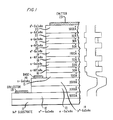
- Exemplary preferred device structure shown in FIG. 1 represents an n-p-n bipolar transistor with two resonant-tunneling double-barrier quantum wells in series in the emitter.
- Such structure can be made by well-established techniques such as, e.g., molecular-beam epitaxy (MBE) or metal-organic chemical vapor deposition (MOCVD), e.g., on an indium phosphide substrate 11 which may be doped or undoped, the latter being preferred in the interest of enhanced device operating speed.
- MBE molecular-beam epitaxy
- MOCVD metal-organic chemical vapor deposition
- Successively deposited lattice-matched layers 12 through 23 have nominal composition Ga 0.47 In 0.53 As in the case of gallium-indium arsenide, and Al 0.48 In 0.52 As in the case of aluminum-indium arsenide.
- Preferred dopant concentrations are greater than or approximately 2x10¹⁸/cm3 for collector-contact layer 12, less than or approximately 2x10¹⁶/cm3 for collector-active layer 13, greater than or approximately 2x10¹⁸/cm3 for base layer 14, approximately 1x10¹⁸/cm3 for layer 15, approximately 5x10¹⁷/cm3 for quantum-well separating layer 19, and greater than or approximately 1x10¹⁸/cm3 for emitter-contact layer 23.
- layers 16, 17, and 18, and layers 20, 21, and 22 form double-barrier resonant-tunneling quantum wells.
- FIG. 1 Not shown in FIG. 1 are 50-Angstrom nominally undoped gallium-indium arsenide offset layers which are preferably included, in the interest of inhibiting dopant diffusion into the barrier layers during high-temperature growth processing, between layers 15 and 16, 18 and 19, 19 and 20, and 22 and 23.
- Photolithography and chemical wet etching were used to produce an emitter mesa having a diameter of approximately 50 micrometers and a base mesa having a diameter of approximately 125 micrometers; the nominal composition of the etchant was 50H2O + 3H3PO4 + 1H2O2.
- Emitter and collector contact metallizations 231 and 121 were made by successively evaporating germanium, gold, silver, and gold; the base contact layer 141 was made by evaporating goldberyllium alloy and then gold.
- the contacts were alloyed at a temperature of approximately 375 degrees C for approximately 10 seconds in a hydrogen atmosphere so as to prevent oxidation. (Oxidation may be prevented also by the use of an inert atmosphere, e.g., of nitrogen or helium.)
- the device structure as described above corresponds to an n-p-n resonant-tunneling bipolar transistor (RTBT), p-n-p structure is not precluded.
- double-barrier quantum-well structures as called for in accordance with the invention are in the conduction band, in the latter case such structures are in the valence band.
- the number of quantum wells present is a plurality of 2 or more, such plurality comprising at least two quantum wells such that, during device operation, quenching of resonant tunneling through these two quantum wells occurs at different base-emitter voltages.
- the two quantum wells are separated such that there is no significant quantum-mechanical interaction between the quantum-mechanical states of the two quantum wells, separation typically resulting from the presence of a sufficiently thick, low-bandgap doped layer between quantum wells.
- Such lower limit on layer thickness is in the interest of precluding the presence of quantum states in the separating layer which are coupled to the quantum states of the quantum wells.
- preferred separating layer thickness is in the range from 500 to 1000 Angstroms for room-temperature operation.
- Preferred doping of the separating layer is at least 2x10¹⁷/cm3.
- Preferred placement of quantum wells is between the base region and the contact to the emitter region; preferred also is the inclusion, adjacent to the base region, of a region having doping type opposite to the doping type of the base region, and having a bandgap which is wider than the bandgap of the base region (see layer 15 in FIG. 1); inclusion of such preferred region serves to inhibit back-injection of minority carriers from the base region during device operation. Conveniently, in the interest of bandgap matching, such region has graded composition towards the quantum wells.
- barrier layers may be made of aluminium-gallium arsenide or aluminum arsenide, and well layers of gallium arsenide or (strained) gallium-indium arsenide, Ga 1-x In x As, 0 ⁇ x ⁇ 0.2. Also, Ga 0.47 In 0.53 As well layers can be combined with aluminum-indium arsenide, indium phosphide, or (strained) aluminum arsenide layers.
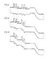
- Device functioning as described below with reference to FIG. 2 to 4 may be understood as based on the sequential quenching of resonant tunneling through two (or more) double-barrier quantum wells as caused by nonuniform electrical field distribution across the quantum wells due to charge build-up. If the collector bias is kept fixed then, for (negative) emitter-base voltages V EB less in magnitude than the build-in voltage of the gallium-indium arsenide p-n junction, most of the bias voltage falls across this junction because its impedance is considerably greater than the impedance of the two quantum wells in series, both of which are conducting via resonant tunneling (as indicated by arrows in FIG. 2).
- V EB If the magnitude of V EB is increased further to equal the build-in voltage, the junction reaches a flat-band configuration and becomes strongly conducting. Any additional increase in the magnitude of V EB will then fall primarily across the quantum wells (see FIG. 3), such wells being designed so that the ground state in the quantum well is significantly above the Fermi level in the adjacent cladding layers.
- the electric field across the quantum well is nonuniform and highest at the aluminum-indium arsenide barrier adjacent to the n-region of the p-n junction (i.e., closest to the base layer) as due to the screening of the field by the charge accumulated in the wells during resonant tunneling.
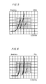
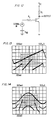
- FIG. 7 Common-emitter output characteristics of the device of FIG. 1 at room temperature are shown in FIG. 7 for base current I B up to 1 mA, in Fig. 8 for I B up to 1.4 mA, and in FIG. 9 for I B up to 1.8 mA.
- I B low V BE
- the applied base-emitter voltage drops mainly across the p-n junction until flat-band condition is reached, the device behaving like a conventional bipolar transistor with a small-signal current gain as high as 70; see FIG. 7.
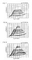
- FIG. 10 and 11 show common-emitter transfer characteristics, I C versus V BE , at constant V CE 2.5 V at respective temperatures of 300 K and 77 K.
- V CE common-emitter transfer characteristics
- V BE increases, the emitter and collector currents increase until the emitter-base junction reaches flat-band condition. Beyond flat-band condition, at higher V BE , resonant tunneling through the two quantum wells quenches sequentially, and sharp drops in the emitter and collector currents are observed.
- the highest peak-to-valley ratio in the transfer characteristics is 4:1 at room temperature, and about 20:1 at 77K.
- the current-voltage characteristics were found to be essentially the same for different values of the collector-base voltage V CE .
- FIG. 15 shows a circuit for parity-bit generation whose operation involves adding up four input bits at the base node of the transistor by the resistive network to generate a stepped waveform.
- the quiescent bias of the transistor adjusted by the resistance R B1 , and the values of the resistance R0 are chosen to select the operating points of the transistor alternately at low and high collector current levels at the successive steps of the summed voltage.
- the output voltage at the collector will be high or low depending on whether the number of input bits set high is even or odd, respectively.
- 24 ordinary transistors are needed in an optimized conventional parity-bit circuit using three exclusive OR's, the circuit according to FIG. 15 performs the same function with a single transistor of the invention.
- conventional parity generators operate by hierarchically comparing two input bits at a time, in the present circuit all input bits are handled simultaneously, and this results in higher operating speed.
- FIG. 15 The circuit of FIG. 15 was tested by means of pseudo-random 4-bit words. Experimental results are shown in FIG. 16 (77 K) and FIG. 17 (room temperature), the top and bottom traces respectively representing the collector output and the base waveforms.
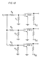
- FIG. 18 shows three devices of the invention combined to form an analog-to-digital converter.
- the analog input V i is applied simultaneously to a parallel array of resonant-tunneling transistors through a plurality of voltage-scaling networks, namely, R0 and R1, R0 and R2, and R0 and R3, to RTBT1, RTBT2, and RTBT3, respectively.
- a parallel array of resonant-tunneling transistors through a plurality of voltage-scaling networks, namely, R0 and R1, R0 and R2, and R0 and R3, to RTBT1, RTBT2, and RTBT3, respectively.
- the outputs from the array form a binary code which represents the quantized analog input level.
- FIG. 19 shows a multiple-valued logic (or multiple-state memory) circuit as based on multiple-valued negative differential resistance characteristic at the emitter-collector terminals of a RTBT when the base-collector junction is held at fixed bias V BC .
- Variations in V CE then cause variations in V EB , causing the collector current to peak as V EB crosses a tunneling resonance; see FIG. 20.
- the resulting load line intersects the current-voltage characteristics at N stable points, where N is the number of resonant peaks.
- the circuit acts as an N-state memory element which can provide high-density data storage. The element can be latched onto any one of the stable states by momentarily applying a voltage close to the desired state.
Abstract
Description
- The invention is concerned with resonant-tunneling semiconductor devices as characterized by device operation involving carrier energy coinciding with a quantized energy level in a potential well.
- The development of resonant-tunneling semiconductor devices has been motivated largely by the desire for increased miniaturization, functional density, and operating speed in electronic devices as designed for use in a variety of digital and analog circuits. Among proposed devices are two-terminal devices as disclosed e.g., by
A. A. Lakhani et al., "Combining Resonant Tunneling Diodes for Signal Processing and Multilevel Logic", Applied Physics Letters, Vol. 52 (1988), pp. 1684-1685;
A. A. Lakhani et al., "Eleven-bit Parity Generator with a Single, Vertically Integrated Resonant Tunneling Device", Electronics Letters, Vol.24 (1988), pp. 681-683;
R. C. Potter et al., "Three-dimensional Integration of Resonant Tunneling Structures for Signal Processing and Three-state Logic", Applied Physics Letters, Vol. 52 (1988), pp. 2163-2164; and
S. Sen et al., "New Resonant-Tunneling Devices with Multiple Negative Resistance Regions and High Room-Temperature Peak-to-Valley Ratio", IEEE Electron Device Letters, Vol. 9 (1988), pp. 402-404. - Proposed also are three-terminal devices as disclosed, e.g., by N. Yokoyama et al., "A New Functional Resonant-Tunneling Hot Electron Transistor (RHET)", Japanese Journal of Applied Physics, Vol. 24 (1985), pp. L853-L854;
F. Capasso et al., "Quantum-Well Resonant Tunneling Bipolar Transistor Operating at Room Temperature", IEEE Electron Device Letters, Vol. EDL-7 (1986), pp. 573-576;
F. Capasso et al., "Resonant Tunneling Gate Field-Effect Transistor", Electronics Letters, Vol. 23 (1987), pp. 225-226; and in
U.S. patent 4,712,121, "High-Speed Semiconductor Device", issued December 8, 1987 to N. Yokoyama. - While such disclosed three-terminal resonant-tunneling devices have single-peak current-voltage characteristics, the invention as described below is motivated by the desire for a transistor having multiple-peak characteristics.
- A semiconductor device is provided for incorporation, e.g., in switching systems, central processor logic units, memories, frequency multipliers, waveform scramblers, parity-bit generators, and analog-to-digital converters, such device being capable, under suitable operating conditions, of a plurality of negative-resistance regions with equal or nearly equal peak currents. The device is a heterostructure bipolar device comprising emitter, base, and collector regions and contacts, the region between the collector region and the contact to the emitter region comprising at least two quantum-well structures. These structures are such that there is no significant quantum-mechanical interaction between their quantum-mechanical states, and such that, during device operation, quenching of resonant tunneling through these quantum wells occurs at different base-emitter voltages.
-
- FIG. 1 is a schematic and greatly enlarged view of an exemplary preferred device structure of the invention and, alongside such structure, a corresponding zero-bias band diagram;
- FIG. 2, 3, and 4 are common-base band diagrams as corresponding to the device of FIG. 1 at fixed collector voltage and successively higher emitter voltage magnitudes;
- FIG. 5 and 6 are common-base transfer-characteristics diagrams as corresponding to the device of FIG. 1 and as obtained, respectively, at the temperature of liquid nitrogen and at room temperature;
- FIG. 7, 8, and 9 are common-emitter output-characteristics diagrams as corresponding to the device of FIG. 1 and as obtained, respectively, at the temperature of liquid nitrogen and at room temperature;
- FIG. 10 and 11 are common-emitter transfer-characteristics diagrams as corresponding to the device of FIG. 1 and as obtained, respectively, at the temperature of liquid nitrogen and at room temperature;
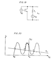
- FIG. 12 is a circuit diagram of a frequency multiplier incorporating the device of FIG. 1;
- FIG. 13 is a diagram of a triangular input waveform to the circuit of FIG. 12 and of the corresponding frequency-multiplied output waveform which, for the sake of clarity, has been inverted in phase;
- FIG. 14 is a diagram of a sinusoidal input waveform to the circuit of FIG. 12 and of the corresponding frequency-multiplied output waveform which, for the sake of clarity, has been inverted in phase;
- FIG. 15 is a diagram of a parity generator incorporating the device of FIG. 1;
- FIG. 16 and 17 are diagrams of base and collector waveforms in the circuit of FIG. 15 as operating, respectively, at the temperature of liquid nitrogen and at room temperature;
- FIG. 18 is a diagram of an analog-to-digital converter incorporating three devices in accordance with FIG. 1;
- FIG. 19 is a diagram of a multi-valued logic circuit incorporating a device in accordance with FIG. 1; and
- FIG. 20 is a current-voltage characteristic diagram as related to the operation of the circuit of FIG. 19.
- Exemplary preferred device structure shown in FIG. 1 represents an n-p-n bipolar transistor with two resonant-tunneling double-barrier quantum wells in series in the emitter. Such structure can be made by well-established techniques such as, e.g., molecular-beam epitaxy (MBE) or metal-organic chemical vapor deposition (MOCVD), e.g., on an indium phosphide substrate 11 which may be doped or undoped, the latter being preferred in the interest of enhanced device operating speed. Successively deposited lattice-matched
layers 12 through 23 have nominal composition Ga0.47In0.53As in the case of gallium-indium arsenide, and Al0.48In0.52As in the case of aluminum-indium arsenide. Preferred dopant concentrations are greater than or approximately 2x10¹⁸/cm³ for collector-contact layer 12, less than or approximately 2x10¹⁶/cm³ for collector-active layer 13, greater than or approximately 2x10¹⁸/cm³ forbase layer 14, approximately 1x10¹⁸/cm³ forlayer 15, approximately 5x10¹⁷/cm³ for quantum-well separatinglayer 19, and greater than or approximately 1x10¹⁸/cm³ for emitter-contact layer 23. As can be seen from the band diagram alongside the device structure,layers layers - Not shown in FIG. 1 are 50-Angstrom nominally undoped gallium-indium arsenide offset layers which are preferably included, in the interest of inhibiting dopant diffusion into the barrier layers during high-temperature growth processing, between
layers - Photolithography and chemical wet etching were used to produce an emitter mesa having a diameter of approximately 50 micrometers and a base mesa having a diameter of approximately 125 micrometers; the nominal composition of the etchant was 50H₂O + 3H₃PO₄ + 1H₂O₂. Emitter and
collector contact metallizations 231 and 121 were made by successively evaporating germanium, gold, silver, and gold; thebase contact layer 141 was made by evaporating goldberyllium alloy and then gold. The contacts were alloyed at a temperature of approximately 375 degrees C for approximately 10 seconds in a hydrogen atmosphere so as to prevent oxidation. (Oxidation may be prevented also by the use of an inert atmosphere, e.g., of nitrogen or helium.) - While the device structure as described above corresponds to an n-p-n resonant-tunneling bipolar transistor (RTBT), p-n-p structure is not precluded. And while, in the former case, double-barrier quantum-well structures as called for in accordance with the invention are in the conduction band, in the latter case such structures are in the valence band. In all cases the number of quantum wells present is a plurality of 2 or more, such plurality comprising at least two quantum wells such that, during device operation, quenching of resonant tunneling through these two quantum wells occurs at different base-emitter voltages. The two quantum wells are separated such that there is no significant quantum-mechanical interaction between the quantum-mechanical states of the two quantum wells, separation typically resulting from the presence of a sufficiently thick, low-bandgap doped layer between quantum wells. Preferred thickness of such separating layer is greater than the thermal de Broglie wavelength of the layer material as defined by λ = h/(3kTm*)1/2, where T denotes the lattice temperature, and m* the effective mass of tunneling (majority) carriers. Such lower limit on layer thickness is in the interest of precluding the presence of quantum states in the separating layer which are coupled to the quantum states of the quantum wells. In the case of gallium-indium arsenide, preferred separating layer thickness is in the range from 500 to 1000 Angstroms for room-temperature operation. Preferred doping of the separating layer is at least 2x10¹⁷/cm³.
- Preferred placement of quantum wells is between the base region and the contact to the emitter region; preferred also is the inclusion, adjacent to the base region, of a region having doping type opposite to the doping type of the base region, and having a bandgap which is wider than the bandgap of the base region (see
layer 15 in FIG. 1); inclusion of such preferred region serves to inhibit back-injection of minority carriers from the base region during device operation. Conveniently, in the interest of bandgap matching, such region has graded composition towards the quantum wells. - While the device of FIG. 1 has been described in terms of preferred gallium-indium arsenide and aluminum-indium arsenide materials, other material compositions are not precluded. For example, barrier layers may be made of aluminium-gallium arsenide or aluminum arsenide, and well layers of gallium arsenide or (strained) gallium-indium arsenide, Ga1-xInxAs, 0≦ x ≦0.2. Also, Ga0.47In0.53As well layers can be combined with aluminum-indium arsenide, indium phosphide, or (strained) aluminum arsenide layers.
- Device functioning as described below with reference to FIG. 2 to 4 may be understood as based on the sequential quenching of resonant tunneling through two (or more) double-barrier quantum wells as caused by nonuniform electrical field distribution across the quantum wells due to charge build-up. If the collector bias is kept fixed then, for (negative) emitter-base voltages VEB less in magnitude than the build-in voltage of the gallium-indium arsenide p-n junction, most of the bias voltage falls across this junction because its impedance is considerably greater than the impedance of the two quantum wells in series, both of which are conducting via resonant tunneling (as indicated by arrows in FIG. 2). If the magnitude of VEB is increased further to equal the build-in voltage, the junction reaches a flat-band configuration and becomes strongly conducting. Any additional increase in the magnitude of VEB will then fall primarily across the quantum wells (see FIG. 3), such wells being designed so that the ground state in the quantum well is significantly above the Fermi level in the adjacent cladding layers. The electric field across the quantum well is nonuniform and highest at the aluminum-indium arsenide barrier adjacent to the n-region of the p-n junction (i.e., closest to the base layer) as due to the screening of the field by the charge accumulated in the wells during resonant tunneling. If VEB is increased further still, resonant tunneling is quenched across the quantum well closest to the indium-gallium arsenide p-n junction, and this process repeats itself for each quantum well in sequence. Once resonant tunneling has been quenched across a quantum well, the voltage drop across such quantum well increased rapidly with increased bias voltage due to increased resistance. The nonresonant tunneling component (i.e., thermionic emission and inelastic tunneling) through the quantum well is large enough to provide continuity for the resonant-tunneling current flowing through the other quantum well(s). Every time resonant tunneling through a quantum well is quenched there is a drop in the electron current injected from the emitter to the base and an attendant drop in the collector current. Thus, a negative transconductance region is obtained in the collector current as a function of VEB, corresponding to the quenching of resonant tunneling through each quantum well. With N quantum wells there will be N peaks in the transfer characteristics.
- In the case of the device of FIG. 1, and as shown in FIG. 5 (corresponding to room-temperature operation) and FIG. 6 (corresponding to operation at a temperature of approximately 77 K), two peaks are observed in the current-voltage characteristics (collector current versus KEB at a fixed collector-base voltage VCB = 0.1 V). For VEB greater in magnitude than the built-in voltage of approximately 0.7 V, the p-n junction begins to conduct strongly and the collector current increases rapidly until resonant tunneling through the first quantum well is quenched. This sequence repeats itself for the second quantum well, thus giving rise to a second peak. The peak-to-valley ratio for the first peak is approximately 4:1 at 300 k, and 3:1 for the second peak. At liquid-nitrogen temperature the corresponding ratios are 22:1 and 8:1. The current-voltage characteristics were found to be essentially the same for different values of the collector-base voltage VCB.
- Common-emitter output characteristics of the device of FIG. 1 at room temperature are shown in FIG. 7 for base current IB up to 1 mA, in Fig. 8 for IB up to 1.4 mA, and in FIG. 9 for IB up to 1.8 mA. At low values of IB (low VBE), the applied base-emitter voltage drops mainly across the p-n junction until flat-band condition is reached, the device behaving like a conventional bipolar transistor with a small-signal current gain as high as 70; see FIG. 7. FIG. 8 shows quenching of current gain at IB = 1.2 mA, with a peak-to-valley ratio of about 6:1. As IB (VBE) is increased further, a second negative-differential-resistance region is produced in the collector-current versus VCE characteristic at IB = 1.6 mA, associated with quenching of resonant tunneling across the other quantum well; see FIG. 9.
- FIG. 10 and 11 show common-emitter transfer characteristics, IC versus VBE, at constant VCE 2.5 V at respective temperatures of 300 K and 77 K. At constant VCE, as VBE increases, the emitter and collector currents increase until the emitter-base junction reaches flat-band condition. Beyond flat-band condition, at higher VBE, resonant tunneling through the two quantum wells quenches sequentially, and sharp drops in the emitter and collector currents are observed. The highest peak-to-valley ratio in the transfer characteristics is 4:1 at room temperature, and about 20:1 at 77K. The current-voltage characteristics were found to be essentially the same for different values of the collector-base voltage VCE.
- Devices of the invention can be used in a variety of circuits as implemented, typically, in the form of integrated circuits. Based on transfer characteristics as shown in FIG. 10 and 11, a frequency multiplier circuit can be designed according to FIG. 12. (For the sake of specificity and convenience, the following feasible values are provided with reference to FIG. 12: VCC = 3.0 V, VBB = 1.8 V, RC = 5 Ω, and RB = 50 Ω.)
- In frequency-multiplier circuit operation, as the imput voltage is increased, the collector current increases and the collector voltage decreases until the device reaches the negative transconductance regions, where a sudden drop in the collector current and an increase in the output voltage are observed. Thus, under suitable bias (VBB), triangular input waves are multiplied by a factor of three (see FIG. 13), and sine waves by a factor of five (see FIG. 14). (For the sake of clarity, output waveforms in FIG. 13 and 14 are shown inverted in phase.) Among specific advantages of the circuit of FIG. 12 is the fact that the output signal is ground-referenced and isolated from the input - as due to multiple peaks in the transfer characteristic of a transistor. Under suitable operating conditions, the circuit of FIG. 12 can alternatively serve for waveform scrambling.
- FIG. 15 shows a circuit for parity-bit generation whose operation involves adding up four input bits at the base node of the transistor by the resistive network to generate a stepped waveform. The quiescent bias of the transistor, adjusted by the resistance RB1, and the values of the resistance R₀ are chosen to select the operating points of the transistor alternately at low and high collector current levels at the successive steps of the summed voltage. Thus, the output voltage at the collector will be high or low depending on whether the number of input bits set high is even or odd, respectively. While 24 ordinary transistors are needed in an optimized conventional parity-bit circuit using three exclusive OR's, the circuit according to FIG. 15 performs the same function with a single transistor of the invention. Moreover, while conventional parity generators operate by hierarchically comparing two input bits at a time, in the present circuit all input bits are handled simultaneously, and this results in higher operating speed.
- The circuit of FIG. 15 was tested by means of pseudo-random 4-bit words. Experimental results are shown in FIG. 16 (77 K) and FIG. 17 (room temperature), the top and bottom traces respectively representing the collector output and the base waveforms.
- FIG. 18 shows three devices of the invention combined to form an analog-to-digital converter. In this application, the analog input Vi is applied simultaneously to a parallel array of resonant-tunneling transistors through a plurality of voltage-scaling networks, namely, R₀ and R₁, R₀ and R₂, and R₀ and R₃, to RTBT1, RTBT2, and RTBT3, respectively. Thus an interlaced pattern of harmonically related transfer characteristics is produced. The outputs from the array form a binary code which represents the quantized analog input level.
- FIG. 19 shows a multiple-valued logic (or multiple-state memory) circuit as based on multiple-valued negative differential resistance characteristic at the emitter-collector terminals of a RTBT when the base-collector junction is held at fixed bias VBC. Variations in VCE then cause variations in VEB, causing the collector current to peak as VEB crosses a tunneling resonance; see FIG. 20. When connected to a resistive load RL and voltage supply VCC, the resulting load line intersects the current-voltage characteristics at N stable points, where N is the number of resonant peaks. Thus, the circuit acts as an N-state memory element which can provide high-density data storage. The element can be latched onto any one of the stable states by momentarily applying a voltage close to the desired state.
Claims (11)
an emitter region having a first conductivity type and a first composition and bandgap profile;
a base region having a second conductivity type and a second composition and bandgap profile;
a collector region having said first conductivity type and having a third composition and bandgap profile;
first, second, and third electrical contacts to said emitter, base, and collector regions, respectively;
a plurality of quantum wells between said collector region and said electrical contact to said emitter region,
CHARACTERIZED IN THAT
at least two of said quantum wells are separated such that there is no significant quantum-mechanical interaction between the quantum-mechanical states of said two quantum wells, and such that, during intended device operation, quenching of resonant tunneling through said quantum wells occurs at different base-emitter voltages.
Applications Claiming Priority (2)
| Application Number | Priority Date | Filing Date | Title |
|---|---|---|---|
| US244753 | 1988-09-14 | ||
| US07/244,753 US4999697A (en) | 1988-09-14 | 1988-09-14 | Sequential-quenching resonant-tunneling transistor |
Publications (2)
| Publication Number | Publication Date |
|---|---|
| EP0359508A2 true EP0359508A2 (en) | 1990-03-21 |
| EP0359508A3 EP0359508A3 (en) | 1990-07-18 |
Family
ID=22923986
Family Applications (1)
| Application Number | Title | Priority Date | Filing Date |
|---|---|---|---|
| EP89309206A Ceased EP0359508A3 (en) | 1988-09-14 | 1989-09-11 | Sequential-quenching resonant-tunneling transistor |
Country Status (5)
| Country | Link |
|---|---|
| US (1) | US4999697A (en) |
| EP (1) | EP0359508A3 (en) |
| JP (1) | JPH0642491B2 (en) |
| KR (1) | KR930004716B1 (en) |
| CA (1) | CA1299769C (en) |
Cited By (3)
| Publication number | Priority date | Publication date | Assignee | Title |
|---|---|---|---|---|
| EP0643489A1 (en) * | 1993-05-24 | 1995-03-15 | Texas Instruments Incorporated | Binary converter |
| US5625205A (en) * | 1993-06-02 | 1997-04-29 | Nec Corporation | Bipolar transistor circuit |
| US6031256A (en) * | 1999-01-05 | 2000-02-29 | National Science Council Of Republic Of China | Wide voltage operation regime double heterojunction bipolar transistor |
Families Citing this family (9)
| Publication number | Priority date | Publication date | Assignee | Title |
|---|---|---|---|---|
| JP3542620B2 (en) * | 1992-09-30 | 2004-07-14 | テキサス インスツルメンツ インコーポレイテツド | Multi-peak resonant tunneling diode |
| USH1570H (en) * | 1993-03-31 | 1996-08-06 | The United States Of America As Represented By The Secretary Of The Army | Variable lateral quantum confinement transistor |
| US5869845A (en) * | 1997-06-26 | 1999-02-09 | Texas Instruments Incorporated | Resonant tunneling memory |
| TW440968B (en) * | 2000-01-10 | 2001-06-16 | Nat Science Council | Heterojunction bipolar transistor device with sun-hat-shaped negative differential resistance characteristic |
| US6995430B2 (en) * | 2002-06-07 | 2006-02-07 | Amberwave Systems Corporation | Strained-semiconductor-on-insulator device structures |
| US20030227057A1 (en) * | 2002-06-07 | 2003-12-11 | Lochtefeld Anthony J. | Strained-semiconductor-on-insulator device structures |
| US7074623B2 (en) * | 2002-06-07 | 2006-07-11 | Amberwave Systems Corporation | Methods of forming strained-semiconductor-on-insulator finFET device structures |
| US20040109692A1 (en) * | 2002-12-09 | 2004-06-10 | James Plante | FSO communication systems having high performance detectors |
| US7026642B2 (en) * | 2003-08-27 | 2006-04-11 | Micron Technology, Inc. | Vertical tunneling transistor |
Citations (2)
| Publication number | Priority date | Publication date | Assignee | Title |
|---|---|---|---|---|
| EP0255288A2 (en) * | 1986-07-31 | 1988-02-03 | AT&T Corp. | Resonant tunneling transistor |
| EP0256759A2 (en) * | 1986-08-04 | 1988-02-24 | Fujitsu Limited | Resonant tunneling semiconductor device |
Family Cites Families (8)
| Publication number | Priority date | Publication date | Assignee | Title |
|---|---|---|---|---|
| JPS6158268A (en) * | 1984-08-30 | 1986-03-25 | Fujitsu Ltd | High speed semiconductor d4evice |
| JPH07105488B2 (en) * | 1986-03-18 | 1995-11-13 | 富士通株式会社 | Semiconductor device |
| GB2191035A (en) * | 1986-05-23 | 1987-12-02 | Philips Electronic Associated | Hot charge-carrier transistors |
| US4845541A (en) * | 1986-05-29 | 1989-07-04 | Regents Of The University Of Minnesota | Tunneling emitter bipolar transistor |
| JPH0642553B2 (en) * | 1986-06-13 | 1994-06-01 | 日本電気株式会社 | Resonant tunnel diode |
| JPH0795675B2 (en) * | 1987-02-14 | 1995-10-11 | 富士通株式会社 | Comparison circuit |
| US4907196A (en) * | 1987-04-28 | 1990-03-06 | Fujitsu Limited | Semiconductor memory device using resonant-tunneling transistor |
| US4912539A (en) * | 1988-08-05 | 1990-03-27 | The University Of Michigan | Narrow-band-gap base transistor structure with dual collector-base barrier including a graded barrier |
-
1988
- 1988-09-14 US US07/244,753 patent/US4999697A/en not_active Expired - Lifetime
-
1989
- 1989-09-08 CA CA000610802A patent/CA1299769C/en not_active Expired - Fee Related
- 1989-09-11 EP EP89309206A patent/EP0359508A3/en not_active Ceased
- 1989-09-12 KR KR1019890013200A patent/KR930004716B1/en not_active IP Right Cessation
- 1989-09-14 JP JP1237408A patent/JPH0642491B2/en not_active Expired - Lifetime
Patent Citations (2)
| Publication number | Priority date | Publication date | Assignee | Title |
|---|---|---|---|---|
| EP0255288A2 (en) * | 1986-07-31 | 1988-02-03 | AT&T Corp. | Resonant tunneling transistor |
| EP0256759A2 (en) * | 1986-08-04 | 1988-02-24 | Fujitsu Limited | Resonant tunneling semiconductor device |
Non-Patent Citations (5)
| Title |
|---|
| I.E.E.E. ELECTRON DEVICE LETTERS, vol. 9, no. 10, October 1988, pages 533-535, IEEE, New York, US; S. SEN et al.: "Multiple-state resonant-tunneling bipolar transistor operating at room temperature and its application as a frequency multiplier" * |
| I.E.E.E. ELECTRON DEVICE LETTERS, vol. 9, no. 8, August 1988, pages 365-367, IEEE, New York, US; T. TANOUE et al.: "A triple-well resonant-tunneling diode for multiple-valued logic application" * |
| IEEE ELECTRON DEVICE LETTERS, vol. 9, no. 5, May 1988, pages 200-202, IEEE, New York, US; J. S\DERSTR\M et al.: "A multiple-state memory cell based on the resonant tunneling diode" * |
| IEEE TRANSACTIONS ON ELECTRON DEVICES, vol. ED-34, no. 10, October 1987, pages 2185-2191, IEEE, New York, US; S. SEN et al.: "Resonant tunneling device with multiple negative differential resistance: Digital and signal processing applications with reduced circuit complexity" * |
| INTERNATIONAL ELECTRON DEVICES MEETING 1988 TECHNICAL DIGEST, San Francisco, CA, 11th-14th December 1988, pages 834-837, IEEE, New York, US; S. SEN et al.: "New resonant tunneling bipolar transistor (RTBT) with multiple negative differential resistance characteristics operating at room temperature with large current gain" * |
Cited By (3)
| Publication number | Priority date | Publication date | Assignee | Title |
|---|---|---|---|---|
| EP0643489A1 (en) * | 1993-05-24 | 1995-03-15 | Texas Instruments Incorporated | Binary converter |
| US5625205A (en) * | 1993-06-02 | 1997-04-29 | Nec Corporation | Bipolar transistor circuit |
| US6031256A (en) * | 1999-01-05 | 2000-02-29 | National Science Council Of Republic Of China | Wide voltage operation regime double heterojunction bipolar transistor |
Also Published As
| Publication number | Publication date |
|---|---|
| US4999697A (en) | 1991-03-12 |
| JPH0642491B2 (en) | 1994-06-01 |
| CA1299769C (en) | 1992-04-28 |
| JPH02114536A (en) | 1990-04-26 |
| KR930004716B1 (en) | 1993-06-03 |
| EP0359508A3 (en) | 1990-07-18 |
| KR900005591A (en) | 1990-04-14 |
Similar Documents
| Publication | Publication Date | Title |
|---|---|---|
| Capasso et al. | Quantum functional devices: resonant-tunneling transistors, circuits with reduced complexity, and multiple valued logic | |
| CA1276275C (en) | Resonant tunneling transistor | |
| Sen et al. | Resonant tunneling device with multiple negative differential resistance: digital and signal processing applications with reduced circuit complexity | |
| US4999697A (en) | Sequential-quenching resonant-tunneling transistor | |
| EP0226383A2 (en) | Resonant-tunneling transistor | |
| Sen et al. | Multiple-state resonant-tunneling bipolar transistor operating at room temperature and its application as a frequency multiplier | |
| KR930002817B1 (en) | Resonant-tunneling device | |
| US4902912A (en) | Apparatus including resonant-tunneling device having multiple-peak current-voltage characteristics | |
| Capasso et al. | Multiple negative transconductance and differential conductance in a bipolar transistor by sequential quenching of resonant tunneling | |
| Chung et al. | Three-terminal Si-based negative differential resistance circuit element with adjustable peak-to-valley current ratios using a monolithic vertical integration | |
| US6303941B1 (en) | Integrated asymmetric resonant tunneling diode pair circuit | |
| Rhee et al. | SiGe resonant tunneling hot‐carrier transistor | |
| Lunardi et al. | Microwave multiple-state resonant tunneling bipolar transistors | |
| Capasso et al. | Quantum transistors and circuits break through the barriers | |
| Potter et al. | A vertically integrated resonant tunneling device with multiple negative differential resistances | |
| CA1284234C (en) | Apparatus including resonant-tunneling device having multiple-peak current-voltage characteristics | |
| Lour et al. | Negative-differential-resistance (NDR) superlattice-emitter transistor | |
| US3482306A (en) | Method of making an esaki means for obtaining high current gain factor | |
| Wallmark et al. | The tunnel resistor | |
| CHO | AND ALFRED zyxwvutsrqponmlkjih | |
| JPS61290759A (en) | Resonance tunnel transistor | |
| Chen et al. | Co-integration of high speed heterojunction bipolar transistors (HBTs) and tunnel diodes | |
| Wei et al. | Effects of base-emitter junction on the resonant tunneling bipolar transistor with double barriers in teh emitter | |
| Sen et al. | Integration of GaAs/AlAs resonant tunneling diodes for digital and analog applications with reduced circuit complexity | |
| Capasso | Quantum electron and optoelectronic devices |
Legal Events
| Date | Code | Title | Description |
|---|---|---|---|
| PUAI | Public reference made under article 153(3) epc to a published international application that has entered the european phase |
Free format text: ORIGINAL CODE: 0009012 |
|
| AK | Designated contracting states |
Kind code of ref document: A2 Designated state(s): DE ES FR GB IT NL |
|
| PUAL | Search report despatched |
Free format text: ORIGINAL CODE: 0009013 |
|
| AK | Designated contracting states |
Kind code of ref document: A3 Designated state(s): DE ES FR GB IT NL |
|
| 17P | Request for examination filed |
Effective date: 19901206 |
|
| 17Q | First examination report despatched |
Effective date: 19930813 |
|
| RAP3 | Party data changed (applicant data changed or rights of an application transferred) |
Owner name: AT&T CORP. |
|
| STAA | Information on the status of an ep patent application or granted ep patent |
Free format text: STATUS: THE APPLICATION HAS BEEN REFUSED |
|
| 18R | Application refused |
Effective date: 19940822 |