EP0361211A2 - Protection circuit for a power semiconductor unit - Google Patents
Protection circuit for a power semiconductor unit Download PDFInfo
- Publication number
- EP0361211A2 EP0361211A2 EP89116976A EP89116976A EP0361211A2 EP 0361211 A2 EP0361211 A2 EP 0361211A2 EP 89116976 A EP89116976 A EP 89116976A EP 89116976 A EP89116976 A EP 89116976A EP 0361211 A2 EP0361211 A2 EP 0361211A2
- Authority
- EP
- European Patent Office
- Prior art keywords
- switching transistor
- emitter
- monitoring
- collector
- base
- Prior art date
- Legal status (The legal status is an assumption and is not a legal conclusion. Google has not performed a legal analysis and makes no representation as to the accuracy of the status listed.)
- Granted
Links
Images

Classifications
-
- H—ELECTRICITY
- H03—ELECTRONIC CIRCUITRY
- H03K—PULSE TECHNIQUE
- H03K17/00—Electronic switching or gating, i.e. not by contact-making and –breaking
- H03K17/08—Modifications for protecting switching circuit against overcurrent or overvoltage
- H03K17/082—Modifications for protecting switching circuit against overcurrent or overvoltage by feedback from the output to the control circuit
- H03K17/0828—Modifications for protecting switching circuit against overcurrent or overvoltage by feedback from the output to the control circuit in composite switches
-
- H—ELECTRICITY
- H03—ELECTRONIC CIRCUITRY
- H03K—PULSE TECHNIQUE
- H03K17/00—Electronic switching or gating, i.e. not by contact-making and –breaking
- H03K17/16—Modifications for eliminating interference voltages or currents
- H03K17/168—Modifications for eliminating interference voltages or currents in composite switches
Definitions
- the invention relates to a protective circuit for a switching transistor with a shutdown device, consisting of a potential-isolating drive converter and a positive and a first negative current source, and a collector-emitter monitoring or base-emitter monitoring.
- the invention relates to a protective circuit for a power semiconductor module, in particular for an IGBT transistor, with a drive stage and a load current monitoring circuit which acts on the latter.
- a protective circuit for a switching transistor with a switch-off device for control pulses of the switching transistor is known from the magazine "Electronics", 1980, number 25, pages 45 to 49.
- the shutdown device is controlled by a comparator, which compares a voltage at the switching transistor with a reference voltage and switches off the control pulses when the switching transistor is overloaded.
- the switching transistor is monitored for desaturation, i.e. it is checked whether a collector-emitter voltage exceeds the value that occurs when the transistor is saturated. The switching transistor can thus be protected against short circuit and overload.
- the voltage applied to the collector-emitter path of the switching transistor is compared in a comparator with a reference voltage corresponding to the saturation value, and the drive pulses are switched off when the collector-emitter voltage of the switching transistor exceeds the saturation value.
- the short-circuit current is switched off or actively limited in the event of a short circuit. Since in switching transistors or high-voltage transistors, the full utilization of the short-circuit strength is made more difficult by the fact that the optimal base clearing current for switching off the switching transistor or high-voltage transistor in the event of a short circuit does not match the optimal base clearing current for switching off under nominal operating conditions, a medium compromise is reached Basic clearing current selected.
- the invention is based on the object of improving the protective circuit of the type mentioned in such a way that the switching transistor is controlled with a respective base clearing current both in the event of a short circuit and under the nominal operating conditions, so that the short-circuit strength of the switching transistor is always fully utilized can.
- the invention has for its object to improve a protective circuit of the type mentioned in such a way that a power semiconductor module, in particular an IGBT transistor, experiences an adapted shutdown in the event of a short circuit, without the power semiconductor or the elements controlled by it being endangered by overvoltages.
- This object is achieved in that the base of the switching transistor is linked to a second negative current source, the current amplitude generated is smaller than that of the first negative current source, and that a control element is provided, the input side with the collector-emitter monitoring and the output side is connected to the power sources.
- the base-emitter path of the switching transistor is provided with two negative current sources, the amplitude values of which differ, one can design one negative current source for the nominal operation and the other negative current source for the event of a short circuit.
- the switching transistors - also called high-voltage transistors - have relatively long storage times, which have a disadvantageous effect on the properties of the devices equipped with these switching transistors, for example converters. Therefore, the switching transistor must be cleared with the highest possible negative basic clearing current, with which the storage times can be kept low.
- a control element that releases the second negative current source so that the switching transistor can be switched off with a base output current matched to the short-circuit strength in the event of a short circuit can. So that this circuit is independent of a monitoring circuit of the switching transistor can always switch this switching transistor off with a first or second negative current, taking into account the full utilization of the short-circuit strength of the switching transistor used, the control element can also be controlled by a base-emitter monitoring of the switching transistor. It is also possible to design the collector-emitter monitoring and the base-emitter monitoring as one structural unit, the outputs of which are linked by means of an OR gate.
- another solution to the problem is that in order to trigger a blocking state of the power semiconductor module, its control input can be switched in each case via one of two resistive paths to a voltage blocking the power semiconductor module, the resistance of the first path triggering a switch-off speed designed for normal operation, while the resistance of the second path triggers a lower shutdown speed for overload operation and the selection of the paths is made by the load current monitoring circuit.
- a switching transistor 2 or high-voltage transistor 2 is connected on the collector side to a supply voltage + U Z.
- This switching transistor 2 can be one of the two switching transistors of a bridge branch of a converter be, wherein the emitter E is then connected to a collector of the second switching transistor of the bridge arm.
- the second switching transistor of the bridge branch or the converter, consisting of several bridge branches is not shown.
- An intermediate circuit feeding the converter can also be provided as the supply voltage source + U Z. If the switching transistor 2 is one of, for example, six switching transistors of a converter, a load, which is not shown for reasons of clarity, can be connected to the collector C or to the emitter E of the switching transistor 2.
- a collector-emitter monitor 6 is connected to the collector G of the switching transistor 2 via a decoupling diode 4, its base B is linked directly to a base-emitter monitor 8.
- the collector-emitter monitoring 6 and the base emitter monitoring 8 are connected to one another by means of an OR gate 10. These two monitors 6 and 8 and the OR gate 10 together form a structural unit 12.
- the switching transistor 2 can also be provided only with the collector-emitter monitor 6 or with the base-emitter monitor 8 without them being one Has influence on the protection circuit according to the invention.
- a positive current source 14, a first negative current source 16 and a second negative current source 18 are also connected to the base B of the switching transistor 2.
- the positive and the first negative current sources 14 and 16 are activated by a potential-isolating converter 20.
- a digital-to-analog converter with potential isolation is provided as the potential-isolating converter 20.
- This converter 20 is supplied with a control signal by means of a line 22 from a speed control or a higher-level control, the speed control or the higher-level control not being shown for reasons of clarity.
- the positive and the first negative current sources 14 and 16 are linked to a control element 24.
- An output signal of the OR gate 10 of the assembly 12 is also fed to this control element 24.
- the control element 24 is linked to the second negative current source 18.
- the switching transistor 2 is provided either only with the collector-emitter monitoring 6 or only with the sasis-emitter monitoring 8, the output of the monitoring is 6 and 8, respectively linked to the control element 24.
- a logic switching device can be provided as the control element 24, for example, which blocks the positive and first negative current sources 14 and 16 as a function of an input signal and releases the second negative current source 18.
- FIG. 2 shows the dependency of the collector current I C on the collector-emitter voltage U CE with a negative base current I B1 , I B2 as a parameter.
- This diagram is referred to in data sheets as "Reverse Bias S.0.A.” designated.
- the hatched area shows a permissible area for pairs of values I C , U CE with a negative base current I B1 .
- the protective circuit it is the task of the protective circuit to ensure that the switching transistor 2 does not leave the permitted hatched area for a predetermined negative base current I B1 , I B2 . If, for example, the switching current I C rises when the switching transistor 2 is switched on, for example due to a short circuit in the load, the switching transistor 2 can only be switched off with a negative base current I B1 or I B2 , so that the switching transistor 2 for a given collector-emitter voltage U CE is not destroyed.
- the nominal collector-emitter voltage U CEN has a value of 800 V and the value of the nominal collector current I CN is approximately 150 A. If you now want to switch off this switching transistor 2 in the nominal operating state, the storage time of the switching transistor 2 should be switched low, the switching transistor 2 must be cleared with the highest possible negative base current I B. According to the diagram, the negative base current I B1 , the value of which is 10 A, can be used as the clearing current without coming out of the hatched area. The closer you get to the solid boundary line G, the higher the utilization of the short-circuit strength.
- the collector current I CK increases to a multiple of the nominal collector current I CN . It is assumed that at nominal collector-emitter Voltage U CEN the short-circuit collector current I CK reaches a value of 400 A. According to the diagram, this operating point I CK , U CEN lies outside the hatched area. This means that the switching transistor 2 is destroyed if the negative base current I B1 is provided as the clearing current. At least this "hard clearing" of the switching transistor 2 leads to constriction effects, as a result of which the transistor loses its ability to be switched off.
- the switching transistor 2 could be switched off with maximum utilization of its short-circuit strength.
- the blocking of the current sources 14 and 16 and the activation of the current source 18 is carried out by the control element 24 as soon as one or the other monitor 6 or 8 supplies a signal.
- a protective circuit for a switching transistor 2 is thus obtained, the short-circuit strength of which can be maximally utilized in the nominal and short-circuit operation.
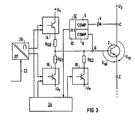
- FIG. 3 shows a schematic basic circuit diagram of the protective circuit according to the invention.
- An IGBT transistor 2 is connected on the collector side to a supply voltage + U Z.
- This IGBT transistor 2 can be one of the two switching transistors of a bridge branch of a converter, the emitter E then being connected to a collector of the second switching transistor of the bridge branch.
- the second switching transistor of the bridge branch or the converter, consisting of several bridge branches, is not shown.
- An intermediate circuit feeding the converter can also be provided as the supply voltage source + U Z.
- the IGBT transistor 2 is one of, for example, six switching transistors of a converter, a load, which is not shown for reasons of clarity, can be connected to the collector C or to the emitter E of the IGBT transistor 2.
- a collector-emitter monitor 6 is connected to the collector C of the IGBT transistor 2 via a decoupling diode 4, its gate G, ie its control input, is directly linked to a gate-emitter monitor 8. Is on the output side the collector-emitter monitoring 6 is connected to the gate-emitter monitoring 8 by means of an OR gate 10. These two monitors 6 and 8 and the OR gate 10 together form a structural unit 12 as a load current monitoring circuit.
- the IGBT transistor 2 could also only be provided with the collector-emitter monitoring 6 or with the gate-emitter monitoring 8, without this affecting the nature of the protective circuit according to the invention.
- the gate G of the IBGT transistor 2 there is also a positive voltage + U v via a resistor R G0 and a switching stage 14 or a negative voltage via a resistor R G1 and a switching stage 16 or a resistor R G2 and a switching stage 18 -U v can be switched on.
- the positive and the negative voltage supply via the switching stages 14 and 16 effective for regular switching operation are activated by a potential-isolating converter 20.
- a digital-to-analog converter with potential isolation is provided for this.
- This converter 20 is supplied with a control signal by means of a line 22 from a speed control or a higher-level control, the speed control or the higher-level control not being shown for reasons of clarity.
- the switching stages 14, 16 and 18 are linked to a control element 24.
- the output signal of the OR gate 10 of the assembly 12 is fed to this control element 24.
- the IGBT transistor 2 were provided either only with the collector-emitter monitoring 6 or only with the gate-emitter monitoring 8, the output of the monitoring 6 or 8 would be linked directly to the input of the control element 24.
- the control element 24 is now designed, for example as a logic switching device, that the switching stages 14 and 16 are blocked in the event of an overload, for example in the event of a short circuit, and the switching stage 18 is released.
- the resistors R G1 and R G2 are designed so that the turn-off speed of the IGBT transistor 2 in the event of an overload compared to the regular shutdown speed.
- the resistance R G2 is chosen larger than the resistance R G1 .
Abstract
Description
Die Erfindung bezieht sich auf eine Schutzschaltung für einen Schalttransistor mit einer Abschalteinrichtung, bestehend aus einem potentialtrennenden Ansteuerwandler und einer positiven und einer ersten negativen Stromquelle, und einer Kollektor-Emitter-Überwachung bzw. Basis-Emitter-Überwachung. Außerdem bezieht sich die Erfindung auf eine Schutzschaltung für einen Leistungshalbleiterbaustein, insbesondere für einen IGBT-Transistor, mit einer Ansteuerstufe und einer auf diese rückwirkenden Laststromüberwachungsschaltung.The invention relates to a protective circuit for a switching transistor with a shutdown device, consisting of a potential-isolating drive converter and a positive and a first negative current source, and a collector-emitter monitoring or base-emitter monitoring. In addition, the invention relates to a protective circuit for a power semiconductor module, in particular for an IGBT transistor, with a drive stage and a load current monitoring circuit which acts on the latter.
Aus der Zeitschrift "Elektronik", 1980, Heft 25, Seiten 45 bis 49 ist eine Schutzschaltung für einen Schalttransistor mit einer Abschalteinrichtung für Ansteuerimpulse des Schalttransistors bekannt. Dabei wird die Abschalteinrichtung von einem Komparator angesteuert, der eine Spannung am Schalttransistor mit einer Referenzspannung vergleicht und die Ansteuerimpulse bei Überlastung des Schalttransistors ausschaltet. Mit einer derartigen Schutzschaltung wird der Schalttransistor auf Entsättigung überwacht, d.h., es wird geprüft, ob eine Kollektor-Emitter-Spannung den bei gesättigtem Transistor auftretenden Wert übersteigt. Damit kann der Schalttransistor gegen Kurzschluß und Überlast geschützt werden. Bei der bekannten Schaltung wird also die an der Kollektor-Emitter-Strecke des Schalttransistors anstehende Spannung in einem Komparator mit einer dem Sättigungswert entsprechenden Referenzspannung verglichen und die Ansteuerimpulse werden abgeschaltet, wenn die Kollektor-Emitter-Spannung des Schalttransistors den Sättigungswert überschreitet.A protective circuit for a switching transistor with a switch-off device for control pulses of the switching transistor is known from the magazine "Electronics", 1980, number 25, pages 45 to 49. The shutdown device is controlled by a comparator, which compares a voltage at the switching transistor with a reference voltage and switches off the control pulses when the switching transistor is overloaded. With such a protective circuit, the switching transistor is monitored for desaturation, i.e. it is checked whether a collector-emitter voltage exceeds the value that occurs when the transistor is saturated. The switching transistor can thus be protected against short circuit and overload. In the known circuit, the voltage applied to the collector-emitter path of the switching transistor is compared in a comparator with a reference voltage corresponding to the saturation value, and the drive pulses are switched off when the collector-emitter voltage of the switching transistor exceeds the saturation value.
Eine weitere Schutzschaltung für Schalttransistoren der eingangs genannten Art ist aus der Zeitschrift "IBM-Technical Disclosure Bulletin", Band 18, Nr. 10, Seiten 3236 bis 3237 bekannt. Bei dieser Schutzschaltung wird die Basis-Emitter-Spannung des Schalttransistors mit einer Referenzspannung eines vergleichenden Mittels verglichen. Als vergleichendes Mittels ist eine Schottky-Diode vorgesehen, deren Anode mit der Basis des Schalttransistors und deren Kathode mit dem Kollektor des Transistors verbunden sind. Beim Ansteigen der Basis-Emitter-Spannung des Schalttransistors wird die Schottky-Diode leitend und führt den überschüssigen Basisstrom des Schalttransistors über einen Transistor und einen Widerstand zum Ausgang.Another protective circuit for switching transistors of the type mentioned at the outset is known from the journal "IBM Technical Disclosure Bulletin",
Mit diesen beiden Schaltungen wird im Falle eines Kurzschlusses der Kurzschlußstrom abgeschaltet oder aktiv begrenzt. Da bei Schalttransistoren bzw. Hochvolttransistoren die volle Ausnutzung der Kurzschlußfestigkeit dadurch erschwert wird, daß der optimale Basis-Ausräumstrom zum Abschalten des Schalttransistors bzw. Hochvolttransistors im Kurzschlußfall nicht mit dem optimalen Basis-Ausräumstrom zum Abschalten unter Nenn-Betriebsbedingungen übereinstimmt, wird als Kompromiß ein mittlerer Basis-Ausräumstrom gewählt.With these two circuits, the short-circuit current is switched off or actively limited in the event of a short circuit. Since in switching transistors or high-voltage transistors, the full utilization of the short-circuit strength is made more difficult by the fact that the optimal base clearing current for switching off the switching transistor or high-voltage transistor in the event of a short circuit does not match the optimal base clearing current for switching off under nominal operating conditions, a medium compromise is reached Basic clearing current selected.
Die gleiche Abschaltproblematik ist auch auf moderne IGBT-Transistoren (IGBT = Insulated-Gate-Bipolar-Transistor) anwendbar. Bie diesen Leistungshalbleitern ist eine MOSFET-Eingangsstufe mit einer bipolaren Ausgangsstufe verbunden. Die Funktionsweise dieser Leistungshalbleiter ist beispielsweise in der Druckschrift "ABB, Abschaltbare Leistungshalbleiter, Technische Information anläßlich einer Fachpressetagung am 06.06.1988 in München" beschrieben.The same is also applicable to modern Abschaltproblematik IGBT transistors (IGBT = I nsulated- G ATE B ipolar- T Transistor). In these power semiconductors, a MOSFET input stage is connected to a bipolar output stage. The way these power semiconductors work is described, for example, in the publication "ABB, Power Semiconductors that can be Disabled, Technical Information on the occasion of a specialist press conference on June 6, 1988 in Munich".
Der Erfindung liegt nun die Aufgabe zugrunde, die Schutzschaltung der eingangs genannten Art dahingehend zu verbessern, daß der Schalttransistor sowohl im Kurzschlußfall als auch unter den Nenn-Betriebsbedingungen mit einem jeweiligen Basis-Ausräumstrom angesteuert wird, so daß die Kurzschlußfestigkeit des Schalttransistors immer voll ausgenutzt werden kann. Außerdem liegt der Erfindung die Aufgabe zugrunde, eine Schutzschaltung der eingangs genannten Art dahingehend zu verbessern, daß ein Leistungshalbleiterbaustein, insbesondere ein IGBT-Transistor, im Kurzschlußfall eine angepaßte Abschaltung erfährt, ohne daß der Leistungshalbleiter oder die von diesem angesteuerten Elemente durch Überspannungen gefährdet werden.The invention is based on the object of improving the protective circuit of the type mentioned in such a way that the switching transistor is controlled with a respective base clearing current both in the event of a short circuit and under the nominal operating conditions, so that the short-circuit strength of the switching transistor is always fully utilized can. In addition, the invention has for its object to improve a protective circuit of the type mentioned in such a way that a power semiconductor module, in particular an IGBT transistor, experiences an adapted shutdown in the event of a short circuit, without the power semiconductor or the elements controlled by it being endangered by overvoltages.
Diese Aufgabe wird erfindungsgemäß dadurch gelöst, daß die Basis des Schalttransistors mit einer zweiten negativen Stromquelle verknüpft ist, deren erzeugte Stromamplitude kleiner ist als die der ersten negativen Stromquelle, und daß ein Steuerglied vorgesehen ist, das eingangsseitig mit der Kollektor-Emitter-Überwachung und ausgangsseitig mit den Stromquellen verbunden ist.This object is achieved in that the base of the switching transistor is linked to a second negative current source, the current amplitude generated is smaller than that of the first negative current source, and that a control element is provided, the input side with the collector-emitter monitoring and the output side is connected to the power sources.
Dadurch, daß die Basis-Emitter-Strecke des Schalttransistors mit zwei negativen Stromquellen versehen ist, deren Amplitudenwerte unterschiedlich sind, kann man die eine negative Stromquelle für den Nenn-Betrieb und die andere negative Stromquelle für den Kurzschlußfall auslegen. Im Nenn-Betrieb bzw. unter normalen Betriebsbedingungen haben die Schalttransistoren - auch Hochvolttransistoren genannt - relativ lange Speicherzeiten, die sich nachteilig auf die Eigenschaften der mit diesen Schalttransistoren ausgerüsteten Geräten, beispielsweise Stromrichter, auswirken. Deshalb muß mit dem höchstmöglichen negativen Basis-Ausräumstrom der Schalttransistor ausgeräumt werden, womit die Speicherzeiten niedrig gehalten werden können.Because the base-emitter path of the switching transistor is provided with two negative current sources, the amplitude values of which differ, one can design one negative current source for the nominal operation and the other negative current source for the event of a short circuit. In nominal operation or under normal operating conditions, the switching transistors - also called high-voltage transistors - have relatively long storage times, which have a disadvantageous effect on the properties of the devices equipped with these switching transistors, for example converters. Therefore, the switching transistor must be cleared with the highest possible negative basic clearing current, with which the storage times can be kept low.
Wegen sehr hoher Stromdichte im Kurzschlußfall würde eine Ansteuerung des Schalttransistors mit dem negativen Basis-Ausräumstrom für den Nenn-Betriebsfall zu Einschnüreffekten führen, wodurch der Schalttransistor die Abschaltfähigkeit verliert und zerstört wird. Um eine hohe Kurzschlußfestigkeit für den Kurzschlußfall zu erhalten, ist es vorteilhaft, gemäß einem Diagramm "Reverse Bias Safe Operating Area" (Reverse Bias S.0.A.), in dem die Abhängigkeit des Kollektorstromes von der Kollektor-Emitter-Spannung mit dem negativen Basisstrom als Parameter gezeigt wird, den Schalttransistor mit einem relativ niedrigen Basis-Ausräumstrom anzusteuern.Because of the very high current density in the event of a short circuit, actuation of the switching transistor with the negative base clearing current for the nominal operating case would lead to constriction effects, as a result of which the switching transistor loses its ability to switch off and is destroyed. To obtain a high short-circuit strength in the event of a short circuit, it is advantageous, according to a diagram "Reverse Bias Safe Operating Area" (Reverse Bias S.0.A.), in which the dependence of the collector current on the collector-emitter voltage with the negative base current is shown as a parameter to control the switching transistor with a relatively low base clearing current.
Damit im Kurzschlußfall die Ansteuerimpulse des Nenn-Betriebes nicht zur Basis des Schalttransistors, insbesondere die negativen Ströme, gelangen, ist ein Steuerglied vorgesehen, daß die zweite negaive Stromquelle freigibt, damit mit einem auf die Kurzschlußfestigkeit im Kurzschlußfall abgestimmter Basis-Ausgangsstrom der Schalttransistor ausgeschaltet werden kann. Damit diese Schaltung unabhängig von einer Überwachungsschaltung des Schalttransistors diesen Schalttransistor immer mit einem ersten bzw. zweiten negativen Strom unter Berücksichtigung der vollen Ausnutzung der Kurzschlußfestigkeit des verwendeten Schalttransistors ausschalten kann, ist das Steuerglied auch von einer Basis-Emitter-Überwachung des Schalttransistors ansteuerbar. Es ist ebenfalls möglich, die Kollektor-Emitter-Überwachung und die Basis-Emitter-Überwachung als eine Baueinheit auszubilden, wobei deren Ausgänge mittels eines ODER-Gatter verknüpft sind.So that in the event of a short circuit the drive pulses of the rated operation do not reach the base of the switching transistor, in particular the negative currents, a control element is provided that releases the second negative current source so that the switching transistor can be switched off with a base output current matched to the short-circuit strength in the event of a short circuit can. So that this circuit is independent of a monitoring circuit of the switching transistor can always switch this switching transistor off with a first or second negative current, taking into account the full utilization of the short-circuit strength of the switching transistor used, the control element can also be controlled by a base-emitter monitoring of the switching transistor. It is also possible to design the collector-emitter monitoring and the base-emitter monitoring as one structural unit, the outputs of which are linked by means of an OR gate.
Eine weitere Lösung der Aufgabe besteht erfindungsgemäß darin, daß zum Auslösen eines Sperrzustandes des Leistungshalbleiterbausteins dessen Steuereingang jeweils über einen von zwei widerstandsbehafteten Pfaden an eine den Leistungshalbleiterbaustein sperrende Spannung schaltbar ist, wobei der Widerstand des ersten Pfades eine für Normalbetrieb ausgelegte Abschaltgeschwindigkeit auslöst, während der Widerstand des zweiten Pfades eine demgegenüber geringere Abschaltgeschwindigkeit für Überlastbetrieb auslöst und wobei die Auswahl der Pfade von der Laststromüberwachungsschaltung getroffen wird.According to the invention, another solution to the problem is that in order to trigger a blocking state of the power semiconductor module, its control input can be switched in each case via one of two resistive paths to a voltage blocking the power semiconductor module, the resistance of the first path triggering a switch-off speed designed for normal operation, while the resistance of the second path triggers a lower shutdown speed for overload operation and the selection of the paths is made by the load current monitoring circuit.
Zur weiteren Erläuterung der Erfindung wird auf die Zeichnung Bezug genommen, in der ein Ausführungsbeispiel einer Schutzschaltung für einen Schalttransistor nach der Erfindung schematisch veranschaulicht ist.
- FIG 1 zeigt eine erfindungsgemäße Schutzschaltung, in
- FIG 2 ist ein Diagramm "Reverse Bias S.0.A." dargestellt, daß die Abhängigkeit des Kollektorstromes von der Kollektor-Emitter-Spannung mit dem negativen Basisstrom als Parameter zeigt und
- FIG 3 veranschaulicht eine erfindungsgemäße Schutzschaltung für einen IGBT-Transistor.
- 1 shows a protective circuit according to the invention, in
- 2 is a diagram "Reverse Bias S.0.A." shown that the dependence of the collector current on the collector-emitter voltage with the negative base current as a parameter shows and
- 3 illustrates an inventive protection circuit for an IGBT transistor.
FIG 1 zeigt das schematisiert Grundschaltbild der erfindungsgemäßen Schutzschaltung. Dabei ist ein Schalttransistor 2 bzw. Hochvolttransistor 2 kollektorseitig an eine Versorgungsspannung +UZ angeschlossen. Dieser Schalttransistor 2 kann einer der beiden Schalttransistoren eines Brückenzweiges eines Stromrichters sein, wobei der Emitter E dann mit einem Kollektor des zweiten Schalttransistors des Brückenzweiges verbunden ist. Aus Übersichtlichkeitsgründen ist der zweite Schalttransistor des Brükkenzweiges bzw. der Stromrichter, bestehend aus mehreren Brückenzweigen nicht dargestellt. Als versorgungsspannungsquelle +UZ kann auch ein den Stromrichter speisender Zwischenkreis vorgesehen sein. Wenn der Schalttransistor 2 einer von beispielsweisen sechs Schalttransistoren eines Stromrichters ist, kann eine Last, die aus Übersichtlichkeitsgründen nicht dargestellt ist, am Kollektor C bzw. am Emitter E des Schalttransistors 2 angeschlossen sein. Über eine Entkopplungsdiode 4 ist eine Kollektor-Emitter-Überwachung 6 mit dem Kollektor G des Schalttransistors 2 verbunden, seine Basis B ist direkt mit einer Basis-Emitter-Überwachung 8 verknüpft. Ausgangsseitig ist die Kollektor-Emitter-Überwachung 6 und die BasisEmitterÜberwachung 8 mittels eines ODER-Gatters 10 miteinander verbunden. Diese beiden Überwachungen 6 und 8 und das ODER-Gatter 10 bilden zusammen eine Baueinheit 12. Jedoch kann der Schalttransistor 2 auch nur mit der Kollektor-Emitter-Überwachung 6 bzw. mit der Basis-Emitter-Überwachung 8 versehen sein, ohne daß sie einen Einfluß auf die erfindungsgemäße Schutzschaltung hat. An der Basis B des Schalttransistors 2 sind außerdem noch eine positive Stromquelle 14, eine erste negative Stromquelle 16 und eine zweite negative Stromquelle 18 angeschlossen. Die positive und die erste negative Stromquelle 14 und 16 werden von einem potentialtrennenden Wandler 20 aktiviert. Als potentialtrennender Wandler 20 ist ein Digital-Analog-Wandler mit Potentialtrennung vorgesehen. Diesem Wandler 20 wird ein Steuersignal mittels einer Leitung 22 aus einer Drehzahl-Regelung bzw. einer übergeordneten Steuerung zugeführt, wobei die Drehzahl-Regelung bzw. die übergeordnete Steuerung aus Übersichtlichkeitsgründen nicht dargestellt ist. Außerdem sind die positive und die erste negative Stromquelle 14 und 16 mit einem Steuerglied 24 verknüpft. Diesem Steuerglied 24 ist ferner auch ein Ausgangssignal des ODER-Gatters 10 der Baueinheit 12 zugeführt. Ausgangsseitig ist das Steuerglied 24 mit der zweiten negativen Stromquelle 18 verknüpft. Wenn jedoch der Schalttransistor 2 entweder nur mit der Kollektor-Emitter-Überwachung 6 oder nur mit der Sasis-Emitter-Überwachung 8 versehen ist, so ist jeweils der Ausgang der Überwachung 6 bzw. 8 mit dem Steuerglied 24 verknüpft. Als Steuerglied 24 kann beispielsweise eine logische Schalteinrichtung vorgesehen sein, die in Abhängigkeit eines Eingangssignals die positive und erste negative Stromquelle 14 und 16 sperrt und die zweite negative Stromquelle 18 freigibt.1 shows the schematic basic circuit diagram of the protective circuit according to the invention. A switching transistor 2 or high-voltage transistor 2 is connected on the collector side to a supply voltage + U Z. This switching transistor 2 can be one of the two switching transistors of a bridge branch of a converter be, wherein the emitter E is then connected to a collector of the second switching transistor of the bridge arm. For reasons of clarity, the second switching transistor of the bridge branch or the converter, consisting of several bridge branches, is not shown. An intermediate circuit feeding the converter can also be provided as the supply voltage source + U Z. If the switching transistor 2 is one of, for example, six switching transistors of a converter, a load, which is not shown for reasons of clarity, can be connected to the collector C or to the emitter E of the switching transistor 2. A collector-
Die Funktion dieser Anordnung wird nachfolgend anhand des Diagramms nach FIG 2 näher erläutert. FIG 2 zeigt die Abhängigkeit des Kollektorstromes IC von der Kollektor-Emitter Spannung UCE mit einem negativen Basisstrom IB1, IB2 als Parameter. Dieses Diagramm wird in Datenblättern als "Reverse Bias S.0.A." bezeichnet. Dabei zeigt der schraffierte Bereich einen zulässigen Bereich für Wertepaare IC, UCE bei einem negativen Basisstrom IB1.The function of this arrangement is explained in more detail below with reference to the diagram according to FIG. 2. 2 shows the dependency of the collector current I C on the collector-emitter voltage U CE with a negative base current I B1 , I B2 as a parameter. This diagram is referred to in data sheets as "Reverse Bias S.0.A." designated. The hatched area shows a permissible area for pairs of values I C , U CE with a negative base current I B1 .
Aufgabe der Schutzschaltung ist es, dafür zu sorgen, daß der Schalttransistor 2 den erlaubten schraffierten Bereich für einen vorbestimmten negativen Basisstrom IB1, IB2 nicht verläßt. Wenn also bei eingeschaltetem Schalttransistor 2 z.B. durch einen Kurzschluß der Last der Kollektorstrom IC ansteigt, so kann der Schalttransistor 2 nur mit einem negativen Basisstrom IB1 bzw. IB2 abgeschaltet werden, damit bei gegebener Kollektor-Emitter-Spannung UCE der Schalttransistor 2 nicht zerstört wird.It is the task of the protective circuit to ensure that the switching transistor 2 does not leave the permitted hatched area for a predetermined negative base current I B1 , I B2 . If, for example, the switching current I C rises when the switching transistor 2 is switched on, for example due to a short circuit in the load, the switching transistor 2 can only be switched off with a negative base current I B1 or I B2 , so that the switching transistor 2 for a given collector-emitter voltage U CE is not destroyed.
Für einen Nenn-Betriebszustand sei angenommen, daß die Nenn-Kollektor-Emitter-Spannung UCEN einen Wert von 800 V hat und der Wert des Nenn-Kollektorstromes ICN ungefähr 150 A beträgt. Wenn man nun diesen Schalttransistor 2 im Nenn-Betriebszustand ausschalten möchte, wobei die Speicherzeit des Schalttransistors 2 niedrig geschaltet werden soll, so muß mit einem höchstmöglichen negativen Basisstrom IB der Schalttransistor 2 ausgeräumt werden. Gemäß dem Diagramm bietet sich als Ausräumstrom der negative Basisstrom IB1 an, dessen Wert 10 A ist, ohne dabei aus dem schraffierten Bereich zu kommen. Je näher man an die durchgezogene Grenzlinie G kommt, umso höher ist die Ausnutzung der Kurzschlußfestigkeit.For a nominal operating state it is assumed that the nominal collector-emitter voltage U CEN has a value of 800 V and the value of the nominal collector current I CN is approximately 150 A. If you now want to switch off this switching transistor 2 in the nominal operating state, the storage time of the switching transistor 2 should be switched low, the switching transistor 2 must be cleared with the highest possible negative base current I B. According to the diagram, the negative base current I B1 , the value of which is 10 A, can be used as the clearing current without coming out of the hatched area. The closer you get to the solid boundary line G, the higher the utilization of the short-circuit strength.
Tritt nun ein Kurzschluß an einer Last auf, so steigt der Kollektorstrom ICK auf ein Mehrfaches des Nenn-Kollektorstromes ICN an. Es wird angenommen, daß bei Nenn-Kollektor-Emitter- Spannung UCEN der Kurzschluß-Kollektorstrom ICK einen Wert von 400 A erreicht. Gemäß dem Diagramm liegt dieser Betriebspunkt ICK, UCEN außerhalb des schraffierten Bereichs. Dies bedeutet, daß der Schalttransistor 2 zerstört wird, wenn als Ausräumstrom der negative Basisstrom IB1 vorgesehen wird. Zumindest führt diese "harte Ausräumung" des Schalttransistors 2 zu Einschnüreffekten, wodurch der Transistor seine Abschaltfähigkeit verliert. Wenn man nun anstelle des negativen Basisstromes IB1 den negativen Basisstrom IB2 bzw. einen negativen Basisstrom, dessen Wert kleiner ist als der Wert des negativen Basisstromes IB2, so könnte der Schalttransistor 2 ausgeschaltet werden bei maximaler Ausnutzung seiner Kurzschlußfestigkeit. Die Sperrung der Stromquellen 14 und 16 und die Aktivierung der Stromquelle 18 erfolgt durch das Steuerglied 24, sobald von der einen oder anderen Überwachung 6 oder 8 ein Signal geliefert wird. Somit erhält man eine Schutzschaltung für einen Schalttransistors 2, dessen Kurzschlußfestigkeit im Nenn- und Kurzschlußbetrieb maximal ausgenutzt werden kann.If there is a short circuit on a load, the collector current I CK increases to a multiple of the nominal collector current I CN . It is assumed that at nominal collector-emitter Voltage U CEN the short-circuit collector current I CK reaches a value of 400 A. According to the diagram, this operating point I CK , U CEN lies outside the hatched area. This means that the switching transistor 2 is destroyed if the negative base current I B1 is provided as the clearing current. At least this "hard clearing" of the switching transistor 2 leads to constriction effects, as a result of which the transistor loses its ability to be switched off. If instead of the negative base current I B1 the negative base current I B2 or a negative base current, the value of which is smaller than the value of the negative base current I B2 , the switching transistor 2 could be switched off with maximum utilization of its short-circuit strength. The blocking of the
Die FIG 3 zeigt ein schematisiertes Grundschaltbild der erfindungsgemßen Schutzschaltung. Dabei ist ein IGBT-Transistor 2 kollektorseitig an eine Versorgungsspannung +UZ angeschlossen. Dieser IGBT-Transistor 2 kann einer der beiden Schalttransistoren eines Brückenzweigs eines Stromrichters sein, wobei der Emitter E dann mit einem Kollektor des zweiten Schalttransistors des Brückenzweigs verbunden ist. Aus Übersichtlichkeitsgründen ist der zweite Schalttransistor des Brückenzweigs bzw. der Stromrichter, bestehend aus mehreren Brückenzweigen nicht dargestellt. Als Versorgungsspannungsquelle +UZ kann auch ein den Stromrichter speisender Zwischenkreis vorgesehen sein.3 shows a schematic basic circuit diagram of the protective circuit according to the invention. An IGBT transistor 2 is connected on the collector side to a supply voltage + U Z. This IGBT transistor 2 can be one of the two switching transistors of a bridge branch of a converter, the emitter E then being connected to a collector of the second switching transistor of the bridge branch. For reasons of clarity, the second switching transistor of the bridge branch or the converter, consisting of several bridge branches, is not shown. An intermediate circuit feeding the converter can also be provided as the supply voltage source + U Z.
Wenn der IGBT-Transistor 2 einer von beispielsweisen sechs Schalttransistoren eines Stromrichters ist, kann eine Last, die aus Übersichtlichkeitsgründen nicht dargestellt ist, am Kollektor C bzw. am Emitter E des IGBT-Transistors 2 angeschlossen sein. Über eine Entkopplungsdiode 4 ist eine Kollektor-Emitter-Überwachung 6 mit dem Kollektor C des IGBT-Transistors 2 verbunden, seine Gate G, d.h. sein Steuereingang, ist direkt mit einer Gate-Emitter-Überwachung 8 verknüpft. Ausgangsseitig ist die Kollektor-Emitter-Überwachung 6 an die Gate-Emitter-Überwachung 8 mittels eines ODER-Gliedes 10 verbunden. Diese beiden Überwachungen 6 und 8 und das ODER-Gliedes 10 bilden zusammen eine Baueinheit 12 als Laststromüberwachungsschaltung. Der IGBT-Transistor 2 könnte allerdings auch nur mit der Kollektor-Emitter-Überwachung 6 bzw. mit der Gate-Emitter-Überwachung 8 versehen sein, ohne daß dies das Wesen der erfindungsgemäßen Schutzschaltung beieinflusen würde. An das Gate G des IBGT-Transistors 2 ist außerdem noch über einen Widerstand RG0 und eine Schaltstufe 14 eine positive Spannung +Uv bzw. über einen Widerstand RG1 und eine Schaltstufe 16 oder einen Widerstand RG2 und eine Schaltstufe 18 eine negative Spannung -Uv anschaltbar.If the IGBT transistor 2 is one of, for example, six switching transistors of a converter, a load, which is not shown for reasons of clarity, can be connected to the collector C or to the emitter E of the IGBT transistor 2. A collector-
Die positive und die negative Spannungsversorgung über die für den regulären Schaltbetrieb wirksamen Schaltstufen 14 und 16 werden von einem potentialtrennenden Wandler 20 aktiviert. Für diesen ist ein Digital-Analog-Wandler mit Potentialtrennung vorgesehen. Diesem Wandler 20 wird ein Steuersignal mittels einer Leitung 22 aus einer Drehzahl-Regelung bzw. einer übergeordneten Steuerung zugeführt, wobei die Drehzahl-Regelung bzw. die übergeordnete Steuerung aus Übersichtlichkeitsgründen nicht dargestellt ist.The positive and the negative voltage supply via the switching stages 14 and 16 effective for regular switching operation are activated by a potential-isolating
Die Schaltstufen 14, 16 und 18 sind mit einem Steuerglied 24 verknüpft. Diesem Steuerglied 24 wird das Ausgangssignal des ODER-Glieds 10 der Baueinheit 12 zugeführt. Wenn jedoch der IGBT-Transistor 2 entweder nur mit der Kollektor-Emitter-Überwachung 6 oder nur mit der Gate-Emitter-Überwachung 8 versehen wäre, so wäre jeweils der Ausgang der Überwachung 6 bzw. 8 direkt mit dem Eingang des Steuerglieds 24 verknüpft. Das Steuerglied 24 ist nun so, beispielsweise als eine logische Schalteinrichtung ausgebildet, daß die im Überlastfall, beispielsweise bei Kurzschluß, die Schaltstufen 14 und 16 gesperrt werden und die Schaltstufe 18 freigegeben wird.The switching stages 14, 16 and 18 are linked to a
Dabei sind die Widerstände RG1 und RG2 so ausgelegt, daß die Abschaltgeschwindigkeit des IGBT-Transistors 2 im Überlastfall gegenüber der regulären Abschaltgeschwindigkeit reduziert wird. Dazu ist der Widerstand RG2 größer gewählt als der Widerstand RG1.The resistors R G1 and R G2 are designed so that the turn-off speed of the IGBT transistor 2 in the event of an overload compared to the regular shutdown speed. For this purpose, the resistance R G2 is chosen larger than the resistance R G1 .
Denkbar wäre es allerdings auch, daß für den Widerstand RG1 ein variabler Widerstand gewählt würde, der je nach Belastung des IGBT-Transistors 2 in Stufen oder kontinuierlich in seinem Widerstandswert erhöht würde. Auf den zweiten Widerstand RG2 könnte dann verzichtet werden. Die zwei Pfade zum Abschalten sind dabei baulich zusammengefaßt.However, it would also be conceivable that a variable resistor would be chosen for the resistor R G1 , which depending on the load on the IGBT transistor 2 would be increased in steps or continuously in its resistance value. The second resistor R G2 could then be dispensed with. The two paths for switching off are structurally combined.
Claims (5)
Priority Applications (1)
| Application Number | Priority Date | Filing Date | Title |
|---|---|---|---|
| AT89116976T ATE100980T1 (en) | 1988-09-28 | 1989-09-13 | PROTECTIVE CIRCUIT FOR A POWER SEMICONDUCTOR MODULE. |
Applications Claiming Priority (4)
| Application Number | Priority Date | Filing Date | Title |
|---|---|---|---|
| DE3832917 | 1988-09-28 | ||
| DE3832917 | 1988-09-28 | ||
| DE3910188 | 1989-03-29 | ||
| DE3910188 | 1989-03-29 |
Publications (3)
| Publication Number | Publication Date |
|---|---|
| EP0361211A2 true EP0361211A2 (en) | 1990-04-04 |
| EP0361211A3 EP0361211A3 (en) | 1990-09-26 |
| EP0361211B1 EP0361211B1 (en) | 1994-01-26 |
Family
ID=25872642
Family Applications (1)
| Application Number | Title | Priority Date | Filing Date |
|---|---|---|---|
| EP89116976A Expired - Lifetime EP0361211B1 (en) | 1988-09-28 | 1989-09-13 | Protection circuit for a power semiconductor unit |
Country Status (2)
| Country | Link |
|---|---|
| EP (1) | EP0361211B1 (en) |
| DE (1) | DE58906812D1 (en) |
Cited By (9)
| Publication number | Priority date | Publication date | Assignee | Title |
|---|---|---|---|---|
| EP0483744A2 (en) * | 1990-11-02 | 1992-05-06 | Hitachi, Ltd. | Current detection circuit of power semiconductor device and power converter using the circuit |
| EP0561386A1 (en) * | 1992-03-18 | 1993-09-22 | Fuji Electric Co., Ltd. | Semiconductor device |
| US5500619A (en) * | 1992-03-18 | 1996-03-19 | Fuji Electric Co., Ltd. | Semiconductor device |
| EP0814564A1 (en) * | 1996-06-20 | 1997-12-29 | ANSALDO INDUSTRIA S.p.A. | Electronic switching circuit with reduction of switching transients |
| WO2000077933A1 (en) * | 1999-06-11 | 2000-12-21 | Siemens Aktiengesellschaft | Circuit comprising a disconnectable power semiconductor switch |
| EP1515440A2 (en) * | 2003-09-05 | 2005-03-16 | Robert Bosch Gmbh | Transistor circuit with voltage limiting circuit using a base emitter resistor |
| CN102723935A (en) * | 2012-05-22 | 2012-10-10 | 柏德胜 | Self-turnoff component driving protection circuit |
| DE102016212211A1 (en) * | 2016-07-05 | 2018-01-11 | Siemens Aktiengesellschaft | Short circuit detection |
| WO2024012743A1 (en) * | 2022-07-14 | 2024-01-18 | Robert Bosch Gmbh | Monitoring device and method for monitoring a reverse converter, reverse converter |
Families Citing this family (1)
| Publication number | Priority date | Publication date | Assignee | Title |
|---|---|---|---|---|
| DE19634612A1 (en) * | 1996-08-27 | 1998-03-12 | Siemens Ag | Method and device for optimizing the switch-off process of a non-latching, switchable power semiconductor switch |
Citations (4)
| Publication number | Priority date | Publication date | Assignee | Title |
|---|---|---|---|---|
| GB2082003A (en) * | 1980-08-08 | 1982-02-24 | Reliance Electric Co | Dual-mode transistor turn-off |
| JPS60100823A (en) * | 1983-11-07 | 1985-06-04 | Nippon Inbaata Kk | Drive circuit of switching transistor |
| EP0190925A2 (en) * | 1985-02-08 | 1986-08-13 | Kabushiki Kaisha Toshiba | A protection circuit for an insulated gate bipolar transistor |
| DE3743453A1 (en) * | 1986-12-24 | 1988-07-28 | Dold & Soehne Kg E | Circuit arrangement for short-circuit protection of a semiconductor amplifier element |
-
1989
- 1989-09-13 DE DE89116976T patent/DE58906812D1/en not_active Expired - Fee Related
- 1989-09-13 EP EP89116976A patent/EP0361211B1/en not_active Expired - Lifetime
Patent Citations (4)
| Publication number | Priority date | Publication date | Assignee | Title |
|---|---|---|---|---|
| GB2082003A (en) * | 1980-08-08 | 1982-02-24 | Reliance Electric Co | Dual-mode transistor turn-off |
| JPS60100823A (en) * | 1983-11-07 | 1985-06-04 | Nippon Inbaata Kk | Drive circuit of switching transistor |
| EP0190925A2 (en) * | 1985-02-08 | 1986-08-13 | Kabushiki Kaisha Toshiba | A protection circuit for an insulated gate bipolar transistor |
| DE3743453A1 (en) * | 1986-12-24 | 1988-07-28 | Dold & Soehne Kg E | Circuit arrangement for short-circuit protection of a semiconductor amplifier element |
Non-Patent Citations (6)
| Title |
|---|
| ELEKTRONIK * |
| ELEKTRONIK Heft 25, 1980, seiten 45-49, DE; K.Rischmueller: "Pulsgesteuerte Treiberstufen für Brückenschaltungen" * |
| IBM TECHNICAL DISCLOSURE BULLETIN * |
| IBM TECHNICAL DISCLOSURE BULLETIN Band 18, nr.10 März 1967, seiten 3236-3237, New York US; S.D.Malaviya: "Self-protected totem pole driver" * |
| PATENT ABSTRACTS OF JAPAN * |
| PATENT ABSTRACTS OF JAPAN Band 9, nr.251 (E-348)(1974) 8 October 1985& JP-A-60100823 * |
Cited By (15)
| Publication number | Priority date | Publication date | Assignee | Title |
|---|---|---|---|---|
| EP0483744A2 (en) * | 1990-11-02 | 1992-05-06 | Hitachi, Ltd. | Current detection circuit of power semiconductor device and power converter using the circuit |
| EP0483744A3 (en) * | 1990-11-02 | 1993-03-17 | Hitachi, Ltd. | Current detection circuit of power semiconductor device and power converter using the circuit |
| EP0561386A1 (en) * | 1992-03-18 | 1993-09-22 | Fuji Electric Co., Ltd. | Semiconductor device |
| US5500619A (en) * | 1992-03-18 | 1996-03-19 | Fuji Electric Co., Ltd. | Semiconductor device |
| EP0730347A2 (en) * | 1992-03-18 | 1996-09-04 | Fuji Electric Co., Ltd. | Semiconductor device |
| EP0730347A3 (en) * | 1992-03-18 | 1996-10-23 | Fuji Electric Co Ltd | Semiconductor device |
| EP0814564A1 (en) * | 1996-06-20 | 1997-12-29 | ANSALDO INDUSTRIA S.p.A. | Electronic switching circuit with reduction of switching transients |
| US6054890A (en) * | 1996-06-20 | 2000-04-25 | Ansaldo Sistemi Industriali S.P.A. | Electronic switching circuit with reduction of switching transients |
| WO2000077933A1 (en) * | 1999-06-11 | 2000-12-21 | Siemens Aktiengesellschaft | Circuit comprising a disconnectable power semiconductor switch |
| EP1515440A2 (en) * | 2003-09-05 | 2005-03-16 | Robert Bosch Gmbh | Transistor circuit with voltage limiting circuit using a base emitter resistor |
| EP1515440A3 (en) * | 2003-09-05 | 2006-05-03 | Robert Bosch Gmbh | Transistor circuit with voltage limiting circuit using a base emitter resistor |
| CN102723935A (en) * | 2012-05-22 | 2012-10-10 | 柏德胜 | Self-turnoff component driving protection circuit |
| DE102016212211A1 (en) * | 2016-07-05 | 2018-01-11 | Siemens Aktiengesellschaft | Short circuit detection |
| DE102016212211B4 (en) | 2016-07-05 | 2019-02-21 | Siemens Aktiengesellschaft | Short circuit detection |
| WO2024012743A1 (en) * | 2022-07-14 | 2024-01-18 | Robert Bosch Gmbh | Monitoring device and method for monitoring a reverse converter, reverse converter |
Also Published As
| Publication number | Publication date |
|---|---|
| EP0361211A3 (en) | 1990-09-26 |
| DE58906812D1 (en) | 1994-03-10 |
| EP0361211B1 (en) | 1994-01-26 |
Similar Documents
| Publication | Publication Date | Title |
|---|---|---|
| EP1410505B1 (en) | Switching device for a switching operation at a high working voltage | |
| DE2638178C2 (en) | Protection device for integrated circuits against overvoltages | |
| DE3001632C2 (en) | ||
| EP0108283A2 (en) | Electronic switch | |
| DE102004057187B4 (en) | inverter circuit | |
| DE102016224706A1 (en) | Gate drive circuit for semiconductor switching devices | |
| EP0620957B1 (en) | Circuit for protecting a mosfet power transistor | |
| DE60128995T2 (en) | Gate driver for thyristor | |
| EP0361211B1 (en) | Protection circuit for a power semiconductor unit | |
| DE4428675A1 (en) | overvoltage protection circuit for MOS power semiconductor switch | |
| EP0690898B1 (en) | Circuit for protecting a power semiconductor switch that may be switched on and off against overvoltages | |
| EP0643485B1 (en) | Circuit arrangement for soft switching off of a FET semiconductor device in case of overcurrent | |
| EP0013710B1 (en) | Push-pull driver, the output of which may be directly connected to the outputs of other drivers | |
| DE4012382C2 (en) | ||
| DE1613705A1 (en) | Power drive circuit | |
| DE3723786C2 (en) | ||
| DE3215589C2 (en) | ||
| EP0560086B1 (en) | Protection circuit for a power-MOSFET driving an inductive load | |
| DE102016210798B3 (en) | Power semiconductor circuit | |
| DE10143432C1 (en) | Driver circuit for field-controlled load switch has control device determining control voltage characteristic during switching in or switching out | |
| EP2020748A2 (en) | Active clamping switch for a high performance semiconductor switch | |
| WO1998012816A1 (en) | Device for reducing short-circuit amplitude of a disconnectable non-latching mos-controlled power semiconductor | |
| DE3536447C2 (en) | Short-circuit and overload-proof transistor output stage | |
| EP0177779B1 (en) | Circuit arrangement with a feeding circuit for feeding a load resistor | |
| WO2000077933A1 (en) | Circuit comprising a disconnectable power semiconductor switch |
Legal Events
| Date | Code | Title | Description |
|---|---|---|---|
| PUAI | Public reference made under article 153(3) epc to a published international application that has entered the european phase |
Free format text: ORIGINAL CODE: 0009012 |
|
| AK | Designated contracting states |
Kind code of ref document: A2 Designated state(s): AT CH DE FR GB IT LI SE |
|
| PUAL | Search report despatched |
Free format text: ORIGINAL CODE: 0009013 |
|
| AK | Designated contracting states |
Kind code of ref document: A3 Designated state(s): AT CH DE FR GB IT LI SE |
|
| 17P | Request for examination filed |
Effective date: 19901009 |
|
| 17Q | First examination report despatched |
Effective date: 19920917 |
|
| GRAA | (expected) grant |
Free format text: ORIGINAL CODE: 0009210 |
|
| AK | Designated contracting states |
Kind code of ref document: B1 Designated state(s): AT CH DE FR GB IT LI SE |
|
| REF | Corresponds to: |
Ref document number: 100980 Country of ref document: AT Date of ref document: 19940215 Kind code of ref document: T |
|
| REF | Corresponds to: |
Ref document number: 58906812 Country of ref document: DE Date of ref document: 19940310 |
|
| ITF | It: translation for a ep patent filed |
Owner name: STUDIO JAUMANN |
|
| ET | Fr: translation filed | ||
| GBT | Gb: translation of ep patent filed (gb section 77(6)(a)/1977) |
Effective date: 19940422 |
|
| PG25 | Lapsed in a contracting state [announced via postgrant information from national office to epo] |
Ref country code: GB Effective date: 19940913 Ref country code: AT Effective date: 19940913 |
|
| PG25 | Lapsed in a contracting state [announced via postgrant information from national office to epo] |
Ref country code: SE Effective date: 19940914 |
|
| PG25 | Lapsed in a contracting state [announced via postgrant information from national office to epo] |
Ref country code: LI Effective date: 19940930 Ref country code: CH Effective date: 19940930 |
|
| PLBE | No opposition filed within time limit |
Free format text: ORIGINAL CODE: 0009261 |
|
| STAA | Information on the status of an ep patent application or granted ep patent |
Free format text: STATUS: NO OPPOSITION FILED WITHIN TIME LIMIT |
|
| 26N | No opposition filed | ||
| EAL | Se: european patent in force in sweden |
Ref document number: 89116976.5 |
|
| GBPC | Gb: european patent ceased through non-payment of renewal fee |
Effective date: 19940913 |
|
| PG25 | Lapsed in a contracting state [announced via postgrant information from national office to epo] |
Ref country code: FR Effective date: 19950531 |
|
| REG | Reference to a national code |
Ref country code: CH Ref legal event code: PL |
|
| EUG | Se: european patent has lapsed |
Ref document number: 89116976.5 |
|
| REG | Reference to a national code |
Ref country code: FR Ref legal event code: ST |
|
| PGFP | Annual fee paid to national office [announced via postgrant information from national office to epo] |
Ref country code: DE Payment date: 19961118 Year of fee payment: 8 |
|
| PG25 | Lapsed in a contracting state [announced via postgrant information from national office to epo] |
Ref country code: DE Free format text: LAPSE BECAUSE OF NON-PAYMENT OF DUE FEES Effective date: 19980603 |
|
| PG25 | Lapsed in a contracting state [announced via postgrant information from national office to epo] |
Ref country code: IT Free format text: LAPSE BECAUSE OF NON-PAYMENT OF DUE FEES;WARNING: LAPSES OF ITALIAN PATENTS WITH EFFECTIVE DATE BEFORE 2007 MAY HAVE OCCURRED AT ANY TIME BEFORE 2007. THE CORRECT EFFECTIVE DATE MAY BE DIFFERENT FROM THE ONE RECORDED. Effective date: 20050913 |