EP0361985A1 - Hybrid microchip bonding article - Google Patents
Hybrid microchip bonding article Download PDFInfo
- Publication number
- EP0361985A1 EP0361985A1 EP89310675A EP89310675A EP0361985A1 EP 0361985 A1 EP0361985 A1 EP 0361985A1 EP 89310675 A EP89310675 A EP 89310675A EP 89310675 A EP89310675 A EP 89310675A EP 0361985 A1 EP0361985 A1 EP 0361985A1
- Authority
- EP
- European Patent Office
- Prior art keywords
- article according
- bonding
- carrier sheet
- article
- tubular
- Prior art date
- Legal status (The legal status is an assumption and is not a legal conclusion. Google has not performed a legal analysis and makes no representation as to the accuracy of the status listed.)
- Granted
Links
Images


Classifications
-
- H—ELECTRICITY
- H05—ELECTRIC TECHNIQUES NOT OTHERWISE PROVIDED FOR
- H05K—PRINTED CIRCUITS; CASINGS OR CONSTRUCTIONAL DETAILS OF ELECTRIC APPARATUS; MANUFACTURE OF ASSEMBLAGES OF ELECTRICAL COMPONENTS
- H05K3/00—Apparatus or processes for manufacturing printed circuits
- H05K3/0011—Working of insulating substrates or insulating layers
- H05K3/0017—Etching of the substrate by chemical or physical means
- H05K3/0026—Etching of the substrate by chemical or physical means by laser ablation
- H05K3/0032—Etching of the substrate by chemical or physical means by laser ablation of organic insulating material
-
- H—ELECTRICITY
- H01—ELECTRIC ELEMENTS
- H01L—SEMICONDUCTOR DEVICES NOT COVERED BY CLASS H10
- H01L23/00—Details of semiconductor or other solid state devices
- H01L23/48—Arrangements for conducting electric current to or from the solid state body in operation, e.g. leads, terminal arrangements ; Selection of materials therefor
- H01L23/488—Arrangements for conducting electric current to or from the solid state body in operation, e.g. leads, terminal arrangements ; Selection of materials therefor consisting of soldered or bonded constructions
- H01L23/498—Leads, i.e. metallisations or lead-frames on insulating substrates, e.g. chip carriers
-
- B—PERFORMING OPERATIONS; TRANSPORTING
- B23—MACHINE TOOLS; METAL-WORKING NOT OTHERWISE PROVIDED FOR
- B23K—SOLDERING OR UNSOLDERING; WELDING; CLADDING OR PLATING BY SOLDERING OR WELDING; CUTTING BY APPLYING HEAT LOCALLY, e.g. FLAME CUTTING; WORKING BY LASER BEAM
- B23K1/00—Soldering, e.g. brazing, or unsoldering
- B23K1/0008—Soldering, e.g. brazing, or unsoldering specially adapted for particular articles or work
- B23K1/0016—Brazing of electronic components
-
- B—PERFORMING OPERATIONS; TRANSPORTING
- B23—MACHINE TOOLS; METAL-WORKING NOT OTHERWISE PROVIDED FOR
- B23K—SOLDERING OR UNSOLDERING; WELDING; CLADDING OR PLATING BY SOLDERING OR WELDING; CUTTING BY APPLYING HEAT LOCALLY, e.g. FLAME CUTTING; WORKING BY LASER BEAM
- B23K20/00—Non-electric welding by applying impact or other pressure, with or without the application of heat, e.g. cladding or plating
- B23K20/02—Non-electric welding by applying impact or other pressure, with or without the application of heat, e.g. cladding or plating by means of a press ; Diffusion bonding
- B23K20/023—Thermo-compression bonding
-
- B—PERFORMING OPERATIONS; TRANSPORTING
- B23—MACHINE TOOLS; METAL-WORKING NOT OTHERWISE PROVIDED FOR
- B23K—SOLDERING OR UNSOLDERING; WELDING; CLADDING OR PLATING BY SOLDERING OR WELDING; CUTTING BY APPLYING HEAT LOCALLY, e.g. FLAME CUTTING; WORKING BY LASER BEAM
- B23K26/00—Working by laser beam, e.g. welding, cutting or boring
- B23K26/36—Removing material
- B23K26/40—Removing material taking account of the properties of the material involved
-
- B—PERFORMING OPERATIONS; TRANSPORTING
- B23—MACHINE TOOLS; METAL-WORKING NOT OTHERWISE PROVIDED FOR
- B23K—SOLDERING OR UNSOLDERING; WELDING; CLADDING OR PLATING BY SOLDERING OR WELDING; CUTTING BY APPLYING HEAT LOCALLY, e.g. FLAME CUTTING; WORKING BY LASER BEAM
- B23K31/00—Processes relevant to this subclass, specially adapted for particular articles or purposes, but not covered by only one of the preceding main groups
- B23K31/02—Processes relevant to this subclass, specially adapted for particular articles or purposes, but not covered by only one of the preceding main groups relating to soldering or welding
-
- G—PHYSICS
- G03—PHOTOGRAPHY; CINEMATOGRAPHY; ANALOGOUS TECHNIQUES USING WAVES OTHER THAN OPTICAL WAVES; ELECTROGRAPHY; HOLOGRAPHY
- G03F—PHOTOMECHANICAL PRODUCTION OF TEXTURED OR PATTERNED SURFACES, e.g. FOR PRINTING, FOR PROCESSING OF SEMICONDUCTOR DEVICES; MATERIALS THEREFOR; ORIGINALS THEREFOR; APPARATUS SPECIALLY ADAPTED THEREFOR
- G03F7/00—Photomechanical, e.g. photolithographic, production of textured or patterned surfaces, e.g. printing surfaces; Materials therefor, e.g. comprising photoresists; Apparatus specially adapted therefor
- G03F7/20—Exposure; Apparatus therefor
- G03F7/2051—Exposure without an original mask, e.g. using a programmed deflection of a point source, by scanning, by drawing with a light beam, using an addressed light or corpuscular source
- G03F7/2053—Exposure without an original mask, e.g. using a programmed deflection of a point source, by scanning, by drawing with a light beam, using an addressed light or corpuscular source using a laser
-
- H—ELECTRICITY
- H01—ELECTRIC ELEMENTS
- H01L—SEMICONDUCTOR DEVICES NOT COVERED BY CLASS H10
- H01L21/00—Processes or apparatus adapted for the manufacture or treatment of semiconductor or solid state devices or of parts thereof
- H01L21/02—Manufacture or treatment of semiconductor devices or of parts thereof
- H01L21/04—Manufacture or treatment of semiconductor devices or of parts thereof the devices having at least one potential-jump barrier or surface barrier, e.g. PN junction, depletion layer or carrier concentration layer
- H01L21/48—Manufacture or treatment of parts, e.g. containers, prior to assembly of the devices, using processes not provided for in a single one of the subgroups H01L21/06 - H01L21/326
- H01L21/4803—Insulating or insulated parts, e.g. mountings, containers, diamond heatsinks
-
- H—ELECTRICITY
- H01—ELECTRIC ELEMENTS
- H01L—SEMICONDUCTOR DEVICES NOT COVERED BY CLASS H10
- H01L21/00—Processes or apparatus adapted for the manufacture or treatment of semiconductor or solid state devices or of parts thereof
- H01L21/02—Manufacture or treatment of semiconductor devices or of parts thereof
- H01L21/04—Manufacture or treatment of semiconductor devices or of parts thereof the devices having at least one potential-jump barrier or surface barrier, e.g. PN junction, depletion layer or carrier concentration layer
- H01L21/48—Manufacture or treatment of parts, e.g. containers, prior to assembly of the devices, using processes not provided for in a single one of the subgroups H01L21/06 - H01L21/326
- H01L21/4814—Conductive parts
- H01L21/4846—Leads on or in insulating or insulated substrates, e.g. metallisation
- H01L21/486—Via connections through the substrate with or without pins
-
- H—ELECTRICITY
- H01—ELECTRIC ELEMENTS
- H01L—SEMICONDUCTOR DEVICES NOT COVERED BY CLASS H10
- H01L23/00—Details of semiconductor or other solid state devices
- H01L23/12—Mountings, e.g. non-detachable insulating substrates
- H01L23/14—Mountings, e.g. non-detachable insulating substrates characterised by the material or its electrical properties
- H01L23/145—Organic substrates, e.g. plastic
-
- H—ELECTRICITY
- H01—ELECTRIC ELEMENTS
- H01L—SEMICONDUCTOR DEVICES NOT COVERED BY CLASS H10
- H01L23/00—Details of semiconductor or other solid state devices
- H01L23/34—Arrangements for cooling, heating, ventilating or temperature compensation ; Temperature sensing arrangements
- H01L23/36—Selection of materials, or shaping, to facilitate cooling or heating, e.g. heatsinks
- H01L23/373—Cooling facilitated by selection of materials for the device or materials for thermal expansion adaptation, e.g. carbon
- H01L23/3733—Cooling facilitated by selection of materials for the device or materials for thermal expansion adaptation, e.g. carbon having a heterogeneous or anisotropic structure, e.g. powder or fibres in a matrix, wire mesh, porous structures
-
- H—ELECTRICITY
- H01—ELECTRIC ELEMENTS
- H01L—SEMICONDUCTOR DEVICES NOT COVERED BY CLASS H10
- H01L23/00—Details of semiconductor or other solid state devices
- H01L23/48—Arrangements for conducting electric current to or from the solid state body in operation, e.g. leads, terminal arrangements ; Selection of materials therefor
- H01L23/488—Arrangements for conducting electric current to or from the solid state body in operation, e.g. leads, terminal arrangements ; Selection of materials therefor consisting of soldered or bonded constructions
- H01L23/498—Leads, i.e. metallisations or lead-frames on insulating substrates, e.g. chip carriers
- H01L23/49827—Via connections through the substrates, e.g. pins going through the substrate, coaxial cables
-
- H—ELECTRICITY
- H01—ELECTRIC ELEMENTS
- H01L—SEMICONDUCTOR DEVICES NOT COVERED BY CLASS H10
- H01L23/00—Details of semiconductor or other solid state devices
- H01L23/48—Arrangements for conducting electric current to or from the solid state body in operation, e.g. leads, terminal arrangements ; Selection of materials therefor
- H01L23/488—Arrangements for conducting electric current to or from the solid state body in operation, e.g. leads, terminal arrangements ; Selection of materials therefor consisting of soldered or bonded constructions
- H01L23/498—Leads, i.e. metallisations or lead-frames on insulating substrates, e.g. chip carriers
- H01L23/49833—Leads, i.e. metallisations or lead-frames on insulating substrates, e.g. chip carriers the chip support structure consisting of a plurality of insulating substrates
-
- H—ELECTRICITY
- H01—ELECTRIC ELEMENTS
- H01L—SEMICONDUCTOR DEVICES NOT COVERED BY CLASS H10
- H01L23/00—Details of semiconductor or other solid state devices
- H01L23/48—Arrangements for conducting electric current to or from the solid state body in operation, e.g. leads, terminal arrangements ; Selection of materials therefor
- H01L23/488—Arrangements for conducting electric current to or from the solid state body in operation, e.g. leads, terminal arrangements ; Selection of materials therefor consisting of soldered or bonded constructions
- H01L23/498—Leads, i.e. metallisations or lead-frames on insulating substrates, e.g. chip carriers
- H01L23/4985—Flexible insulating substrates
-
- H—ELECTRICITY
- H01—ELECTRIC ELEMENTS
- H01L—SEMICONDUCTOR DEVICES NOT COVERED BY CLASS H10
- H01L24/00—Arrangements for connecting or disconnecting semiconductor or solid-state bodies; Methods or apparatus related thereto
- H01L24/01—Means for bonding being attached to, or being formed on, the surface to be connected, e.g. chip-to-package, die-attach, "first-level" interconnects; Manufacturing methods related thereto
- H01L24/50—Tape automated bonding [TAB] connectors, i.e. film carriers; Manufacturing methods related thereto
-
- B—PERFORMING OPERATIONS; TRANSPORTING
- B23—MACHINE TOOLS; METAL-WORKING NOT OTHERWISE PROVIDED FOR
- B23K—SOLDERING OR UNSOLDERING; WELDING; CLADDING OR PLATING BY SOLDERING OR WELDING; CUTTING BY APPLYING HEAT LOCALLY, e.g. FLAME CUTTING; WORKING BY LASER BEAM
- B23K2101/00—Articles made by soldering, welding or cutting
- B23K2101/36—Electric or electronic devices
- B23K2101/40—Semiconductor devices
-
- B—PERFORMING OPERATIONS; TRANSPORTING
- B23—MACHINE TOOLS; METAL-WORKING NOT OTHERWISE PROVIDED FOR
- B23K—SOLDERING OR UNSOLDERING; WELDING; CLADDING OR PLATING BY SOLDERING OR WELDING; CUTTING BY APPLYING HEAT LOCALLY, e.g. FLAME CUTTING; WORKING BY LASER BEAM
- B23K2103/00—Materials to be soldered, welded or cut
- B23K2103/30—Organic material
- B23K2103/42—Plastics
-
- B—PERFORMING OPERATIONS; TRANSPORTING
- B23—MACHINE TOOLS; METAL-WORKING NOT OTHERWISE PROVIDED FOR
- B23K—SOLDERING OR UNSOLDERING; WELDING; CLADDING OR PLATING BY SOLDERING OR WELDING; CUTTING BY APPLYING HEAT LOCALLY, e.g. FLAME CUTTING; WORKING BY LASER BEAM
- B23K2103/00—Materials to be soldered, welded or cut
- B23K2103/50—Inorganic material, e.g. metals, not provided for in B23K2103/02 – B23K2103/26
-
- H—ELECTRICITY
- H01—ELECTRIC ELEMENTS
- H01L—SEMICONDUCTOR DEVICES NOT COVERED BY CLASS H10
- H01L24/00—Arrangements for connecting or disconnecting semiconductor or solid-state bodies; Methods or apparatus related thereto
- H01L24/80—Methods for connecting semiconductor or other solid state bodies using means for bonding being attached to, or being formed on, the surface to be connected
- H01L24/86—Methods for connecting semiconductor or other solid state bodies using means for bonding being attached to, or being formed on, the surface to be connected using tape automated bonding [TAB]
-
- H—ELECTRICITY
- H01—ELECTRIC ELEMENTS
- H01L—SEMICONDUCTOR DEVICES NOT COVERED BY CLASS H10
- H01L2924/00—Indexing scheme for arrangements or methods for connecting or disconnecting semiconductor or solid-state bodies as covered by H01L24/00
- H01L2924/10—Details of semiconductor or other solid state devices to be connected
- H01L2924/11—Device type
- H01L2924/12—Passive devices, e.g. 2 terminal devices
- H01L2924/1204—Optical Diode
- H01L2924/12042—LASER
-
- H—ELECTRICITY
- H01—ELECTRIC ELEMENTS
- H01L—SEMICONDUCTOR DEVICES NOT COVERED BY CLASS H10
- H01L2924/00—Indexing scheme for arrangements or methods for connecting or disconnecting semiconductor or solid-state bodies as covered by H01L24/00
- H01L2924/10—Details of semiconductor or other solid state devices to be connected
- H01L2924/11—Device type
- H01L2924/14—Integrated circuits
-
- H—ELECTRICITY
- H01—ELECTRIC ELEMENTS
- H01L—SEMICONDUCTOR DEVICES NOT COVERED BY CLASS H10
- H01L2924/00—Indexing scheme for arrangements or methods for connecting or disconnecting semiconductor or solid-state bodies as covered by H01L24/00
- H01L2924/30—Technical effects
- H01L2924/301—Electrical effects
- H01L2924/3011—Impedance
-
- H—ELECTRICITY
- H05—ELECTRIC TECHNIQUES NOT OTHERWISE PROVIDED FOR
- H05K—PRINTED CIRCUITS; CASINGS OR CONSTRUCTIONAL DETAILS OF ELECTRIC APPARATUS; MANUFACTURE OF ASSEMBLAGES OF ELECTRICAL COMPONENTS
- H05K1/00—Printed circuits
- H05K1/02—Details
- H05K1/03—Use of materials for the substrate
- H05K1/0313—Organic insulating material
- H05K1/032—Organic insulating material consisting of one material
- H05K1/0326—Organic insulating material consisting of one material containing O
-
- H—ELECTRICITY
- H05—ELECTRIC TECHNIQUES NOT OTHERWISE PROVIDED FOR
- H05K—PRINTED CIRCUITS; CASINGS OR CONSTRUCTIONAL DETAILS OF ELECTRIC APPARATUS; MANUFACTURE OF ASSEMBLAGES OF ELECTRICAL COMPONENTS
- H05K1/00—Printed circuits
- H05K1/02—Details
- H05K1/03—Use of materials for the substrate
- H05K1/0313—Organic insulating material
- H05K1/032—Organic insulating material consisting of one material
- H05K1/0333—Organic insulating material consisting of one material containing S
-
- H—ELECTRICITY
- H05—ELECTRIC TECHNIQUES NOT OTHERWISE PROVIDED FOR
- H05K—PRINTED CIRCUITS; CASINGS OR CONSTRUCTIONAL DETAILS OF ELECTRIC APPARATUS; MANUFACTURE OF ASSEMBLAGES OF ELECTRICAL COMPONENTS
- H05K1/00—Printed circuits
- H05K1/02—Details
- H05K1/03—Use of materials for the substrate
- H05K1/0313—Organic insulating material
- H05K1/032—Organic insulating material consisting of one material
- H05K1/0346—Organic insulating material consisting of one material containing N
-
- H—ELECTRICITY
- H05—ELECTRIC TECHNIQUES NOT OTHERWISE PROVIDED FOR
- H05K—PRINTED CIRCUITS; CASINGS OR CONSTRUCTIONAL DETAILS OF ELECTRIC APPARATUS; MANUFACTURE OF ASSEMBLAGES OF ELECTRICAL COMPONENTS
- H05K1/00—Printed circuits
- H05K1/02—Details
- H05K1/03—Use of materials for the substrate
- H05K1/0313—Organic insulating material
- H05K1/0353—Organic insulating material consisting of two or more materials, e.g. two or more polymers, polymer + filler, + reinforcement
- H05K1/036—Multilayers with layers of different types
-
- H—ELECTRICITY
- H05—ELECTRIC TECHNIQUES NOT OTHERWISE PROVIDED FOR
- H05K—PRINTED CIRCUITS; CASINGS OR CONSTRUCTIONAL DETAILS OF ELECTRIC APPARATUS; MANUFACTURE OF ASSEMBLAGES OF ELECTRICAL COMPONENTS
- H05K2201/00—Indexing scheme relating to printed circuits covered by H05K1/00
- H05K2201/01—Dielectrics
- H05K2201/0104—Properties and characteristics in general
- H05K2201/0116—Porous, e.g. foam
-
- H—ELECTRICITY
- H05—ELECTRIC TECHNIQUES NOT OTHERWISE PROVIDED FOR
- H05K—PRINTED CIRCUITS; CASINGS OR CONSTRUCTIONAL DETAILS OF ELECTRIC APPARATUS; MANUFACTURE OF ASSEMBLAGES OF ELECTRICAL COMPONENTS
- H05K2201/00—Indexing scheme relating to printed circuits covered by H05K1/00
- H05K2201/01—Dielectrics
- H05K2201/0137—Materials
- H05K2201/0154—Polyimide
-
- H—ELECTRICITY
- H05—ELECTRIC TECHNIQUES NOT OTHERWISE PROVIDED FOR
- H05K—PRINTED CIRCUITS; CASINGS OR CONSTRUCTIONAL DETAILS OF ELECTRIC APPARATUS; MANUFACTURE OF ASSEMBLAGES OF ELECTRICAL COMPONENTS
- H05K2201/00—Indexing scheme relating to printed circuits covered by H05K1/00
- H05K2201/10—Details of components or other objects attached to or integrated in a printed circuit board
- H05K2201/10227—Other objects, e.g. metallic pieces
- H05K2201/10378—Interposers
-
- H—ELECTRICITY
- H05—ELECTRIC TECHNIQUES NOT OTHERWISE PROVIDED FOR
- H05K—PRINTED CIRCUITS; CASINGS OR CONSTRUCTIONAL DETAILS OF ELECTRIC APPARATUS; MANUFACTURE OF ASSEMBLAGES OF ELECTRICAL COMPONENTS
- H05K2203/00—Indexing scheme relating to apparatus or processes for manufacturing printed circuits covered by H05K3/00
- H05K2203/10—Using electric, magnetic and electromagnetic fields; Using laser light
- H05K2203/107—Using laser light
Landscapes
- Engineering & Computer Science (AREA)
- Physics & Mathematics (AREA)
- Microelectronics & Electronic Packaging (AREA)
- Power Engineering (AREA)
- General Physics & Mathematics (AREA)
- Computer Hardware Design (AREA)
- Condensed Matter Physics & Semiconductors (AREA)
- Mechanical Engineering (AREA)
- Manufacturing & Machinery (AREA)
- Optics & Photonics (AREA)
- Plasma & Fusion (AREA)
- Ceramic Engineering (AREA)
- Chemical & Material Sciences (AREA)
- Materials Engineering (AREA)
- Wire Bonding (AREA)
- Non-Reversible Transmitting Devices (AREA)
- Packages (AREA)
- Adhesive Tapes (AREA)
- Adhesives Or Adhesive Processes (AREA)
- Electric Connection Of Electric Components To Printed Circuits (AREA)
Abstract
Description
- This invention relates to a hybrid bonding article which can be provided in arrangements suitable for use in tape-automated bonding (TAB) of semiconductor microcircuits (microchips).
- Known TAB devices have a structure akin to that shown schematically in the accompanying sketch A. A polymer tape A1 having edge sprocket holes A2 for feeding the tape in automated bonding equipment carries a series of arrays (one shown) of conductive tracks A3 arranged in a pattern suitable for bonding their inner ends A4 to the bonding sites of a microchip (not shown). The tape A1 is cut away under the ends A4 of the tracks so that the ends project as unsupported "fingers" over the cut-away space A5. Bonding is effected by bending the fingers into the space A5 to make contact with the chip positioned against the opposite side of the tape from that carrying the tracks. This is followed by bonding by known techniques which often require the chip bonding sites to "bumped" with bonding material, e.g. solder.
- The present invention can avoid such disadvantageous "bumping" processes.
- Another form of TAB device known as "area TAB" is described in U.S. Patents 3832769, 3868724 and 4472876, in which the conductive tracks do not project as "fingers", but instead are connected to solid metal terminals formed in holes passing through the tape material. The terminals project from the surface of the tape remote from the tracks and can therefore make electrical contact with bonding sites on micro chips or other devices brought into contact therewith. The reliability of the electrical contacts thus established may be limited by the relative rigidity of the terminals hindering their ability to conform to variations in height of the bonding sites on the chip, especially as increasing miniaturization and complexity of microchips requires bonding sites in central areas of the chip as well as around its edges.
- The present invention alleviates these problems by means of an ingenious hybrid form of TAB article, and accordingly provides in one of its aspects a tape-automated bonding article comprising a carrier sheet carrying at least one array of electrically conductive tracks having ends arranged for bonding to a microcircuit device, each such bondable track end being supported by the carrier sheet material and being electrically connected to a surface region of the carrier material not carrying that track end by a tubular formation of electrically conductive material within, preferably plated within, at least one connecting hole of diameter less than 200 micrometres, preferably less than 100 micrometres, more preferably less than 50 micrometres. The holes will usually pass more or less straight through the sheet to its opposite surface (i.e., the "surface region not carrying the track end"), but may be sloping or indirect (e.g. curved) if desired. Preferably, the tubular conductive material in the connecting hole or holes projects beyond the said surface region so as to facilitate bonding to the microcircuit, and this may be achieved by removing one or more layers from the carrier sheet after plating (or other provision) of the conductive material in the connecting hole.
- The use of a tubular formation of conductive material (preferably metal) in the connecting holes has considered advantages over the known solid metal terminals. The tubes may crumple when compressed longitudinally against a microchip or other device, thus taking up irregularities without the major deviation from the longitudinal axis which normally results when solid columns or wires are so compressed. Also, solder or other fusible material may be provided at or within the ends (at least) of the tubes to facilitate thermal bonding and electrical connection.
- This hybrid TAB article according to the invention may be constructed with cut-away "fingers" of the carrier sheet material supporting the conductive track ends to be bonded, thus providing a "fingered" construction corresponding to, but with advantages over, the ordinary TAB article; or may be constructed with "fingers" extending also to the central regions of the chip. These "fingered" hybrids may be regarded as a separate aspect of the invention, for which alternative forms of connection (e.g. solid wires or posts) may also be useful. Cutting away the carrier is not essential, since the tubular projections from the connecting holes can be arranged to render unnecessary the bending of the track ends, but the "fingered" construction may provide advantageous flexibility in articles with central, as well as peripheral, connection sites.
- An example of a fingered construction accordingly to the present invention is illustrated schematically in Figure 1 of the accompanying drawings, wherein the reference numerals correspond to the numerals used in Sketch A.
- The connecting holes with the tubular electrically conductive material, preferably metal, therein, one or more per track end, cannot be made by the methods described in the known "area TAB" patents mentioned above. The present invention preferably hybridizes the TAB concept with methods and materials for making self-supporting uniaxial connectors described in any one or more of copending British Patent Applications 8802567, 8802565, 8802566, 8802568, 8815447.1, and European Published Patent Applications EP-A-0213774, 0327399, 0329314 and 0327398, the disclosures of all of which are incorporated herein by reference. Laser ablation drilling of a layered polymer sheet and metal plating within the hole(s) followed by removal of one or more soluble layers from the sheet (to expose the ends of the metal tubes thus formed within the holes) is preferred. The resulting hybrid TAB article incorporating in situ tubular uniaxial connectors, with the metal TAB tracks preferably subsequently applied to its surface, represents a significant commercial advance, as aforesaid, over previously proposed TAB articles.
- These and other aspects of the invention are illustrated in the largely self-explanatory Figures 2 to 7 of the accompanying drawings, and the invention includes any novel sub-set or sub-combination of the features disclosed in the drawings or description of this specification.
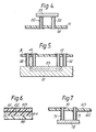
- Figure 2 illustrates schematically the use of a TAB article according to the invention with central connection sites but without the easily envisaged cut-away "fingers".
Metal tubes 21 project from holes through apolyimide sheet 22, withconductive tracks 23 connecting to the tubes. A standard unbumped I.C. is shown in position for thermocompression (or other) bonding to the hybrid TAB article. - Figure 3 illustrates shcematically a TAB production line in which a
polyimide tape article 31 according to the invention with projecting platedmetal tubes 32 is assembled with unbumpedintegrated circuit chips 33. Thetape 31 is fed from left to right (as shown) by means not shown, passing underguides 35, and is bonded to thechips 33, feeding from right to left, by thermode 34. - Figure 4 shows in more detail part of the TAB article and chip of Fig. 3 (inverted), with
metal tracks 41 on the surface oftape 31. - Figure 5 shows a TAB article with a
chip 33 inset in asupport substrate 51, themetal tubes 32 in this case electrically bridging, via thetracks 41, between thechip 33 and thesubstrate 51. - Figure 6 shows a multilayer polymer/metal laminate suitable for making a multi-level TAB article (see Fig 7) according to the invention. Copper track-forming
layers polyimide sheet 63, with an optionalfurther layer 64 of polyimide and a soluble layer 65 (e.g. of polyamide). The polyimide and soluble polymer layers may be those described in the aforementioned British applications and published European applications. - Figure 7 shows the use of a multi-level hybrid TAB article made by drilling and plating the laminate of Fig. 6, (
optional layer 64 omitted) followed by removal of thesoluble polymer layer 65. Such a structure permits closer spacing of themetal tubes 71 to connect to high density I.C. 72 (standard unbumped form). - The hybrid TAB articles according to the present invention can advantageously be impedance matched with the other circuitry to be connected. Multi-layer articles (e.g. Fig 7) could advantageously separate signals from power, and very fine separation (pitch) between tracks may be achieved.
- When the sheet which ultimately contains the conductive through-holes (as distinct from any removable surface layers on such a sheet) is to comprise a polyimide material, a preferred polymer material is a substantially fully cyclised polyimide capable of retaining at least 50%, preferably at least 75%, more preferably at least 85%, of its original elongation after immersion in water of pH10 at 100°C for 4 days according to ASTM D882. It will be readily understood that a "substantially fully cyclised" polyimide is one having substantially no open imide rings or uncyclised amic acid groupings. Such a polyimide is better able to survive hot alkaline metal plating baths, which attack incompletely cyclised polyimides such as Kapton (TM).
- The currently preferred commercially available polyimides are those available under the Trade Mark "UPILEX" from Ube/ICI. One of these, "UPILEX R", is believed to be a relatively completely cyclised polymer having a repeat unit derived from biphenyl dianhydride and diaminodiphenylether, viz.

- Preferred, however, is "UPILEX S", which is believed to have a repeat unit derived from the same anhydride and phenylene diamine, viz.

Claims (9)
Applications Claiming Priority (4)
| Application Number | Priority Date | Filing Date | Title |
|---|---|---|---|
| GB888823057A GB8823057D0 (en) | 1988-09-30 | 1988-09-30 | Hybrid microchip bonding article |
| GB8823057 | 1988-09-30 | ||
| GB888828245A GB8828245D0 (en) | 1988-12-02 | 1988-12-02 | Anisotropically electrically conductive articles |
| GB8828245 | 1988-12-02 |
Publications (2)
| Publication Number | Publication Date |
|---|---|
| EP0361985A1 true EP0361985A1 (en) | 1990-04-04 |
| EP0361985B1 EP0361985B1 (en) | 1994-12-07 |
Family
ID=26294463
Family Applications (2)
| Application Number | Title | Priority Date | Filing Date |
|---|---|---|---|
| EP89911588A Pending EP0436652A1 (en) | 1988-09-30 | 1989-09-29 | Hybrid microchip bonding article |
| EP89310675A Expired - Lifetime EP0361985B1 (en) | 1988-09-30 | 1989-09-29 | Hybrid microchip bonding article |
Family Applications Before (1)
| Application Number | Title | Priority Date | Filing Date |
|---|---|---|---|
| EP89911588A Pending EP0436652A1 (en) | 1988-09-30 | 1989-09-29 | Hybrid microchip bonding article |
Country Status (7)
| Country | Link |
|---|---|
| US (1) | US5254811A (en) |
| EP (2) | EP0436652A1 (en) |
| JP (1) | JP2873032B2 (en) |
| KR (1) | KR900702568A (en) |
| AT (1) | ATE115335T1 (en) |
| DE (1) | DE68919792T2 (en) |
| WO (1) | WO1990003662A1 (en) |
Cited By (2)
| Publication number | Priority date | Publication date | Assignee | Title |
|---|---|---|---|---|
| EP0502710A1 (en) * | 1991-03-04 | 1992-09-09 | Texas Instruments Incorporated | Flexible film semiconductor package |
| FR2730657A1 (en) * | 1995-02-22 | 1996-08-23 | Solaic Sa | METHOD AND INSTALLATION FOR MAKING HOLES IN THE INSULATING FILM OF A SUPPORT TAPE FOR ELECTRONIC BOARD MODULES |
Families Citing this family (11)
| Publication number | Priority date | Publication date | Assignee | Title |
|---|---|---|---|---|
| US5455390A (en) * | 1994-02-01 | 1995-10-03 | Tessera, Inc. | Microelectronics unit mounting with multiple lead bonding |
| US6429112B1 (en) | 1994-07-07 | 2002-08-06 | Tessera, Inc. | Multi-layer substrates and fabrication processes |
| US5688716A (en) | 1994-07-07 | 1997-11-18 | Tessera, Inc. | Fan-out semiconductor chip assembly |
| US5830782A (en) * | 1994-07-07 | 1998-11-03 | Tessera, Inc. | Microelectronic element bonding with deformation of leads in rows |
| US6828668B2 (en) * | 1994-07-07 | 2004-12-07 | Tessera, Inc. | Flexible lead structures and methods of making same |
| US5518964A (en) * | 1994-07-07 | 1996-05-21 | Tessera, Inc. | Microelectronic mounting with multiple lead deformation and bonding |
| US6117694A (en) * | 1994-07-07 | 2000-09-12 | Tessera, Inc. | Flexible lead structures and methods of making same |
| US5798286A (en) * | 1995-09-22 | 1998-08-25 | Tessera, Inc. | Connecting multiple microelectronic elements with lead deformation |
| KR19990007929A (en) | 1995-04-26 | 1999-01-25 | 데이빗로스클리블랜드 | Multi-faced repeated exposure method and apparatus |
| US6133072A (en) * | 1996-12-13 | 2000-10-17 | Tessera, Inc. | Microelectronic connector with planar elastomer sockets |
| US6735387B1 (en) | 2001-01-10 | 2004-05-11 | Tim Schnell | Motion detector camera |
Citations (3)
| Publication number | Priority date | Publication date | Assignee | Title |
|---|---|---|---|---|
| EP0171232A2 (en) * | 1984-08-09 | 1986-02-12 | Minnesota Mining And Manufacturing Company | Area-bonding tape |
| EP0213774A1 (en) * | 1985-08-05 | 1987-03-11 | Raychem Limited | Anisotropically electrically conductive article |
| EP0279769A2 (en) * | 1987-02-17 | 1988-08-24 | Rogers Corporation | Electrical substrate material, multilayer circuit and integrated circuit chip carrier package comprising said material |
Family Cites Families (6)
| Publication number | Priority date | Publication date | Assignee | Title |
|---|---|---|---|---|
| US4177519A (en) * | 1975-07-28 | 1979-12-04 | Sharp Kabushiki Kaisha | Electronic control assembly mounted on a flexible carrier and manufacture thereof |
| NL7610306A (en) * | 1976-09-16 | 1978-03-20 | Du Pont | CONTACT DEVICE FOR AN INTEGRATED CIRCUIT. |
| FR2404990A1 (en) * | 1977-10-03 | 1979-04-27 | Cii Honeywell Bull | SUBSTRATE FOR THE INTERCONNECTION OF ELECTRONIC COMPONENTS WITH INTEGRATED CIRCUITS, EQUIPPED WITH A REPAIR DEVICE |
| US4540226A (en) * | 1983-01-03 | 1985-09-10 | Texas Instruments Incorporated | Intelligent electronic connection socket |
| JP2641869B2 (en) * | 1987-07-24 | 1997-08-20 | 三菱電機株式会社 | Method for manufacturing semiconductor device |
| FR2620586A1 (en) * | 1987-09-14 | 1989-03-17 | Em Microelectronic Marin Sa | METHOD FOR MANUFACTURING ELECTRONIC MODULES, IN PARTICULAR FOR MICROCIRCUIT CARDS |
-
1989
- 1989-09-29 WO PCT/GB1989/001158 patent/WO1990003662A1/en not_active Application Discontinuation
- 1989-09-29 KR KR1019900701136A patent/KR900702568A/en not_active Application Discontinuation
- 1989-09-29 EP EP89911588A patent/EP0436652A1/en active Pending
- 1989-09-29 AT AT89310675T patent/ATE115335T1/en not_active IP Right Cessation
- 1989-09-29 US US07/671,789 patent/US5254811A/en not_active Expired - Lifetime
- 1989-09-29 JP JP1510808A patent/JP2873032B2/en not_active Expired - Fee Related
- 1989-09-29 DE DE68919792T patent/DE68919792T2/en not_active Expired - Fee Related
- 1989-09-29 EP EP89310675A patent/EP0361985B1/en not_active Expired - Lifetime
Patent Citations (3)
| Publication number | Priority date | Publication date | Assignee | Title |
|---|---|---|---|---|
| EP0171232A2 (en) * | 1984-08-09 | 1986-02-12 | Minnesota Mining And Manufacturing Company | Area-bonding tape |
| EP0213774A1 (en) * | 1985-08-05 | 1987-03-11 | Raychem Limited | Anisotropically electrically conductive article |
| EP0279769A2 (en) * | 1987-02-17 | 1988-08-24 | Rogers Corporation | Electrical substrate material, multilayer circuit and integrated circuit chip carrier package comprising said material |
Cited By (3)
| Publication number | Priority date | Publication date | Assignee | Title |
|---|---|---|---|---|
| EP0502710A1 (en) * | 1991-03-04 | 1992-09-09 | Texas Instruments Incorporated | Flexible film semiconductor package |
| FR2730657A1 (en) * | 1995-02-22 | 1996-08-23 | Solaic Sa | METHOD AND INSTALLATION FOR MAKING HOLES IN THE INSULATING FILM OF A SUPPORT TAPE FOR ELECTRONIC BOARD MODULES |
| WO1996026039A1 (en) * | 1995-02-22 | 1996-08-29 | Solaic | Method and apparatus for making holes in an insulating film on a carrier strip for electronic card modules |
Also Published As
| Publication number | Publication date |
|---|---|
| DE68919792D1 (en) | 1995-01-19 |
| WO1990003662A1 (en) | 1990-04-05 |
| JP2873032B2 (en) | 1999-03-24 |
| EP0361985B1 (en) | 1994-12-07 |
| KR900702568A (en) | 1990-12-07 |
| DE68919792T2 (en) | 1995-08-03 |
| ATE115335T1 (en) | 1994-12-15 |
| JPH04501486A (en) | 1992-03-12 |
| EP0436652A1 (en) | 1991-07-17 |
| US5254811A (en) | 1993-10-19 |
Similar Documents
| Publication | Publication Date | Title |
|---|---|---|
| US5254811A (en) | Hybrid microchip bonding article | |
| US6574113B2 (en) | Electronic package with stacked connections and method for making same | |
| CN102612252B (en) | Printed wiring board | |
| TW522536B (en) | Bumpless flip chip assembly with strips-in-via and plating | |
| US4814855A (en) | Balltape structure for tape automated bonding, multilayer packaging, universal chip interconnection and energy beam processes for manufacturing balltape | |
| US5601678A (en) | Method for providing electrical interconnections between adjacent circuit board layers of a multi-layer circuit board | |
| US5994773A (en) | Ball grid array semiconductor package | |
| US5631447A (en) | Uses of uniaxially electrically conductive articles | |
| EP0117348B1 (en) | Bonding leads to semiconductor devices | |
| US5637925A (en) | Uses of uniaxially electrically conductive articles | |
| US5861322A (en) | Process for manufacturing an interconnection substrate to connect a chip onto a reception substrate | |
| EP0139431B1 (en) | Method of mounting a carrier for a microelectronic silicon chip | |
| CA1321659C (en) | Uses of uniaxially electrically conductive articles | |
| KR930002909B1 (en) | Area-bonding tape | |
| EP0327399A1 (en) | Method of manufacturing an uniaxially electrically conductive article | |
| WO1984002248A1 (en) | Method of connecting double-sided circuits | |
| CN101578929A (en) | Printed wiring board and method for manufacturing the same | |
| CN107230640A (en) | Have radiating seat and the heat-dissipating gain-type semiconductor subassembly and its preparation method of double build-up circuitries | |
| JP2006245195A (en) | Double-sided printed wiring board | |
| JPH08264914A (en) | Fpc with thermocompression bonded bump | |
| JPH0923055A (en) | Electronic circuit board | |
| JPH11145622A (en) | Multi-layer interconnection substrate | |
| JPH06224255A (en) | Semiconductor element packaging insulation film and packaging structure for carrier and semiconductor element |
Legal Events
| Date | Code | Title | Description |
|---|---|---|---|
| PUAI | Public reference made under article 153(3) epc to a published international application that has entered the european phase |
Free format text: ORIGINAL CODE: 0009012 |
|
| 17P | Request for examination filed |
Effective date: 19891023 |
|
| AK | Designated contracting states |
Kind code of ref document: A1 Designated state(s): ES |
|
| RBV | Designated contracting states (corrected) |
Designated state(s): AT BE CH DE ES FR GB IT LI NL SE |
|
| XX | Miscellaneous (additional remarks) |
Free format text: VERBUNDEN MIT 89911588.5/0436652 (EUROPAEISCHE ANMELDENUMMER/VEROEFFENTLICHUNGSNUMMER) DURCH ENTSCHEIDUNG VOM 14.08.92. |
|
| 17Q | First examination report despatched |
Effective date: 19921028 |
|
| GRAA | (expected) grant |
Free format text: ORIGINAL CODE: 0009210 |
|
| AK | Designated contracting states |
Kind code of ref document: B1 Designated state(s): AT BE CH DE ES FR GB IT LI NL SE |
|
| PG25 | Lapsed in a contracting state [announced via postgrant information from national office to epo] |
Ref country code: IT Free format text: LAPSE BECAUSE OF FAILURE TO SUBMIT A TRANSLATION OF THE DESCRIPTION OR TO PAY THE FEE WITHIN THE PRE;WARNING: LAPSES OF ITALIAN PATENTS WITH EFFECTIVE DATE BEFORE 2007 MAY HAVE OCCURRED AT ANY TIME BEFORE 2007. THE CORRECT EFFECTIVE DATE MAY BE DIFFERENT FROM THE ONE RECORDED.SCRIBED TIME-LIMIT Effective date: 19941207 Ref country code: NL Effective date: 19941207 Ref country code: LI Effective date: 19941207 Ref country code: BE Effective date: 19941207 Ref country code: ES Free format text: THE PATENT HAS BEEN ANNULLED BY A DECISION OF A NATIONAL AUTHORITY Effective date: 19941207 Ref country code: AT Effective date: 19941207 Ref country code: CH Effective date: 19941207 |
|
| REF | Corresponds to: |
Ref document number: 115335 Country of ref document: AT Date of ref document: 19941215 Kind code of ref document: T |
|
| XX | Miscellaneous (additional remarks) |
Free format text: VERBUNDEN MIT 89911588.5/0436652 (EUROPAEISCHE ANMELDENUMMER/VEROEFFENTLICHUNGSNUMMER) DURCH ENTSCHEIDUNG VOM 14.08.92. |
|
| REF | Corresponds to: |
Ref document number: 68919792 Country of ref document: DE Date of ref document: 19950119 |
|
| ET | Fr: translation filed | ||
| PG25 | Lapsed in a contracting state [announced via postgrant information from national office to epo] |
Ref country code: SE Effective date: 19950307 |
|
| REG | Reference to a national code |
Ref country code: CH Ref legal event code: PL |
|
| NLV1 | Nl: lapsed or annulled due to failure to fulfill the requirements of art. 29p and 29m of the patents act | ||
| PLBE | No opposition filed within time limit |
Free format text: ORIGINAL CODE: 0009261 |
|
| STAA | Information on the status of an ep patent application or granted ep patent |
Free format text: STATUS: NO OPPOSITION FILED WITHIN TIME LIMIT |
|
| 26N | No opposition filed | ||
| REG | Reference to a national code |
Ref country code: GB Ref legal event code: IF02 |
|
| PGFP | Annual fee paid to national office [announced via postgrant information from national office to epo] |
Ref country code: FR Payment date: 20060918 Year of fee payment: 18 |
|
| PGFP | Annual fee paid to national office [announced via postgrant information from national office to epo] |
Ref country code: GB Payment date: 20060925 Year of fee payment: 18 |
|
| PGFP | Annual fee paid to national office [announced via postgrant information from national office to epo] |
Ref country code: DE Payment date: 20061031 Year of fee payment: 18 |
|
| GBPC | Gb: european patent ceased through non-payment of renewal fee |
Effective date: 20070929 |
|
| PG25 | Lapsed in a contracting state [announced via postgrant information from national office to epo] |
Ref country code: DE Free format text: LAPSE BECAUSE OF NON-PAYMENT OF DUE FEES Effective date: 20080401 |
|
| REG | Reference to a national code |
Ref country code: FR Ref legal event code: ST Effective date: 20080531 |
|
| PG25 | Lapsed in a contracting state [announced via postgrant information from national office to epo] |
Ref country code: FR Free format text: LAPSE BECAUSE OF NON-PAYMENT OF DUE FEES Effective date: 20071001 |
|
| PG25 | Lapsed in a contracting state [announced via postgrant information from national office to epo] |
Ref country code: GB Free format text: LAPSE BECAUSE OF NON-PAYMENT OF DUE FEES Effective date: 20070929 |