EP0363500A1 - Circuit arrangement for the correction of digital signals received in an analogous form - Google Patents
Circuit arrangement for the correction of digital signals received in an analogous form Download PDFInfo
- Publication number
- EP0363500A1 EP0363500A1 EP88116127A EP88116127A EP0363500A1 EP 0363500 A1 EP0363500 A1 EP 0363500A1 EP 88116127 A EP88116127 A EP 88116127A EP 88116127 A EP88116127 A EP 88116127A EP 0363500 A1 EP0363500 A1 EP 0363500A1
- Authority
- EP
- European Patent Office
- Prior art keywords
- coefficient
- digital signals
- digital
- adder
- multiplier
- Prior art date
- Legal status (The legal status is an assumption and is not a legal conclusion. Google has not performed a legal analysis and makes no representation as to the accuracy of the status listed.)
- Granted
Links
Images
Classifications
-
- H—ELECTRICITY
- H04—ELECTRIC COMMUNICATION TECHNIQUE
- H04L—TRANSMISSION OF DIGITAL INFORMATION, e.g. TELEGRAPHIC COMMUNICATION
- H04L25/00—Baseband systems
- H04L25/02—Details ; arrangements for supplying electrical power along data transmission lines
- H04L25/03—Shaping networks in transmitter or receiver, e.g. adaptive shaping networks
- H04L25/03006—Arrangements for removing intersymbol interference
- H04L25/03012—Arrangements for removing intersymbol interference operating in the time domain
- H04L25/03114—Arrangements for removing intersymbol interference operating in the time domain non-adaptive, i.e. not adjustable, manually adjustable, or adjustable only during the reception of special signals
- H04L25/03133—Arrangements for removing intersymbol interference operating in the time domain non-adaptive, i.e. not adjustable, manually adjustable, or adjustable only during the reception of special signals with a non-recursive structure
Definitions
- the invention relates to a circuit arrangement according to the preamble of claim 1.
- circuit arrangements are already known (for example: NTG technical reports 88, "Ways to Integrated Communication Network", pages 50 to 57) for digital signals that are transmitted by an analog transmission method and are subject to distortions caused by pre-oscillators of subsequent digital signals as well as by post-oscillators of previously received digital signals. Strong linear distortions occur in particular in the case of digital subscriber connections in ISDN (Integrated Services Digital Network), which must be eliminated by corresponding equalization measures in digital signal receiving devices.
- the distortion caused by pre-oscillators is generally low. For example, a transversal filter with two to four fit coefficients is sufficient for equalization. In contrast, distortions caused by ringing are very large.
- equalizers can be compensated, for example, with a decision feedback equalizer.
- the number of equalizer coefficients here is in the range from 20 to 40.
- the object outlined above is achieved in a circuit arrangement according to the preamble of claim 1 by features specified in the characterizing part of this claim.
- the invention has the advantage that the post-oscillation distortions are also reduced in the pre-oscillator equalizer with little additional circuitry complexity, so that this convergence and stability behavior of the post-oscillator equalizer is improved.
- the secondary coefficients For the design of the pre-oscillator equalizer, it has proven to be expedient for the secondary coefficients to be adaptively adjustable and for the fixed factor A to be fixed at 1/2 or as an integral factor.
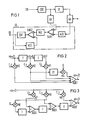
- the digital subscriber line device shown in FIG. 1 may be designed, for example, for a duplex transmission of digital signals over a two-wire line using the same method.
- a subscriber line device for example, first transmits binary signals SD to be transmitted as message signals over the two-wire line using a Encoder COD converted into multi-stage signals, for example in digital signals coded according to the 2BlQ line code and emitted as analog signals via a fork arrangement GA after pulse shaping in a pulse shaper IF.
- Analog signals to be picked up from the relevant subscriber line device via the two-wire line first pass through the already mentioned fork arrangement GA and then arrive at the digital signal receiving device EE shown in FIG.
- the input of this receiving device is formed by an analog / digital converter A / D, which takes samples from the analog signals supplied to it, for example at a distance corresponding to a bit length of the transmitted digital signals, and converts them into a predetermined number of bits.
- the necessary sampling clock pulses are provided by a clock generator, not shown.
- the digital signals provided by the analog / digital converter are then successively fed to a subtractor SUB1, which is simultaneously acted upon with compensation signals from an echo canceller EK.
- These compensation signals compensate for echo signal components contained in the digital signals, which are superimposed on the received analog signals in the previously described delivery of digital signals in analog form via the two-wire line by reflections on this line or by incomplete decoupling of the transmission paths of the fork arrangement.
- the compensated digital signals are then forwarded for further processing, if necessary via a control amplifier (not shown) to an equalizer arrangement, which largely eliminates the distortions of the digital signals caused by the electrical properties of the two-wire line.
- the equalizer arrangement has, for example, a pre-oscillator equalizer VEZ, the output of which signals are fed to a subtractor SUB2.
- a second input of this subtractor is connected to the output of a post-oscillation equalizer NEZ.
- this equalizer is connected to the output of a decision-maker ENT, which is connected downstream of the subtractor SUB2.
- the equalized digital signals ED occurring at the output of this decision-maker are then fed to further devices (not shown in FIG. 1) for further evaluation.
- FIG. 1 shows a first exemplary embodiment for the pre-oscillator equalizer VEZ shown in FIG.
- This equalizer is designed as a transversal filter, in which three successive digital signals x (n), x (n + 1) and x (n + 2) are taken into account for the equalization, which occur at the sampling times n, n + 1, n + 2 .
- These digital signals are fed to two delay elements T connected in series, each of which causes a delay time corresponding to the time interval between two successive digital signals.
- the digital signal x (n + 2) thus occurs at the input of the transversal filter simultaneously with the digital signals x (n + 1) and x (n) present at the outputs of the two delay elements T.
- These digital signals are fed to three separate multipliers M1, M2 and M3.
- the outputs of these multipliers are connected to inputs of an adder ADD1, which has at its output a pre-oscillation caused by the digital signals x (n + 1) and x (n + 2). Distortion-free digital signal y (n + 2).
- the output of the multiplier M2 is additionally connected to a multiplier M4 via a delay element 2T, which causes a delay time which is twice that of the delay elements T mentioned.
- This multiplier is also loaded with a fixed factor A and is connected on the output side to a further input of the adder ADD1 already mentioned.
- the signal fed to the adder in this way additionally reduces the post-oscillation distortions contained in the digital signal x (n) and caused by the digital signal x (n-1) occurring at the point in time n-1.
- FIG. 3 shows a further exemplary embodiment for the pre-oscillator equalizer VEZ shown in FIG.
- the successive digital signals are simultaneously fed to three separate multipliers M5, M6 and M7.
- the multiplier M7 is also acted upon by the main coefficient C0.
- the multiplier M6 or M5 however, the secondary coefficient C Mau1 or C ⁇ 2 is supplied.
- each of the multipliers is connected to an input of an adder having a total of two inputs.
- the adder connected to the multiplier M7 is designated ADD4 in FIG.
- the adder designated the multiplier M6 or M5 bears the designation ADD3 or ADD2.
- the output of the multiplier M6 is additionally connected to a further multiplier M8 to which a fixed factor A is applied.
- this multiplier is connected via a delay element T to the second input of the adder ADD4.
- the second input of the adder ADD3 assigned to the multiplier M6, on the other hand, is connected to the output of the adder ADD4 via a delay element T.
- the output of the adder ADD3 is delayed with the second input of the adder ADD2 tion member T in connection.
- the delay elements just mentioned each cause a delay time which corresponds to the time interval between two successive digital signals.
- the transversal filter shown in FIG. 3 also frees, on the one hand, a digital signal x (n) occurring at time n from the pre-oscillation distortions contained in it, caused by the digital signals x (n + 1) and x (n + 2), and on the other hand the Reduced the proportion of ringing distortions caused by the digital signal x (n-1).
- the secondary coefficients C ⁇ 1 and C ⁇ 2, however, can be adaptively adjustable. Since any known methods can be used for this adaptive setting, no further explanation is given here. Regardless of the choice of the method for adaptive adjustment, it is expedient to set the previously mentioned factor A with 1/2 or as an integral factor, for example 1, 2 or 3.
Abstract
Description
Die Erfindung betrifft eine Schaltungsanordnung gemäß Oberbegriff des Patentanspruches 1. Derartige Schaltungsanordnungen sind bereits bekannt (z. B: NTG-Fachberichte 88, "Wege zum integrierten Kommunikationsnetz", Seiten 50 bis 57), um Digitalsignale, die durch ein analoges Übertragungsverfahren übertragen werden und dabei sowohl durch Vorschwinger nachfolgender Digitalsignale als auch durch Nachschwinger zuvor empfangener Digitalsignale verursachten Verzerrungen unterworfen sind, zu entzerren. Dabei treten insbesondere bei digitalen Teilnehmeranschlüssen in ISDN (Integrated Services Digital Network) starke lineare Verzerrungen auf, die durch entsprechende Entzerrungsmaßnahmen in Digitalsignal-Empfangseinrichtungen beseitigt werden müssen. Die durch Vorschwinger verursachten Verzerrungen sind im allgemeinen gering. Zur Entzerrung ist beispielsweise ein Transversalfilter mit zwei bis vier Fiterkoeffizienten ausreichend. Verzerrungen, die durch Nachschwinger verursacht sind, sind demgegenüber sehr groß. Sie lassen sich beispielsweise mit einem entscheidungsrückgekoppelten Entzerrer kompensieren. Die Anzahl der Entzerrerkoeffizienten liegt hier im Bereich von 20 bis 40. Bei höherwertigen Digitalsignalen, wie z. B. bei nach einem 2BlQ-Leitungscode codierten Digitalsignalen, können jedoch in derartigen Entzerrern bei starken Verzerrungen Konvergenz- und Stabilitätsprobleme auftreten.The invention relates to a circuit arrangement according to the preamble of
Es ist nun Aufgabe der vorliegenden Erfindung, einen Weg zu zeigen, wie bei einer Schaltungsanordnung gemäß Oberbegriff des Patentanspruches 1 das Konvergenz- und Stabilitätsverhalten verbessert werden kann.It is an object of the present invention to show a way in which the convergence and stability behavior can be improved in a circuit arrangement according to the preamble of
Gelöst wird die vorstehend aufgezeigte Aufgabe bei einer Schaltungsanordnung gemäß Oberbegriff des Patentanspruches 1 durch die im kennzeichnenden Teil dieses Patentanspruches angegebenen Merkmale. Die Erfindung bringt den Vorteil mit sich, daß mit einem geringen zusätzlichen schaltungstechnischen Aufwand in dem Vorschwinger-Entzerrer auch bereits die Nachschwinger-Verzerrungen reduziert werden, so daß durch diese Reduzierung das Konvergenz und Stabilitätsverhalten des Nachschwinger-Entzerrers verbessert ist.The object outlined above is achieved in a circuit arrangement according to the preamble of
Gemäß den Patentansprüchen 2 und 3 sind zwei hinsichtlich des schaltungstechnischen Aufwandes besonders günstige Ausführungsbeispiele für einen Vorschwinger-Entzerrer angegeben.According to
Für die Auslegung des Vorschwinger-Entzerrers hat es sich als zweckmäßig erwiesen, daß die Nebenkoeffizienten adaptiv einstellbar sind und der festgelegte Faktor A mit 1/2 oder als ganzzahliger Faktor festgelegt ist.For the design of the pre-oscillator equalizer, it has proven to be expedient for the secondary coefficients to be adaptively adjustable and for the fixed factor A to be fixed at 1/2 or as an integral factor.
Im folgenden wird nun die vorliegende Erfindung anhand von Zeichnungen beispielsweise näher erläutert.
- FIG 1 zeigt in einem Blockschaltbild eine digitale Teilnehmeranschluß-Einrichtung, bei der die Erfindung angewandt ist,
- FIG 2 zeigt ein erstes Ausführungsbeispiel für einen Vorschwinger-Entzerrer und
- FIG 3 zeigt ein zweites Ausführungsbeispiel für einen Vorschwinger-Entzerrer.
- 1 shows a block diagram of a digital subscriber line device to which the invention is applied,
- 2 shows a first exemplary embodiment of a pre-oscillator equalizer and
- 3 shows a second exemplary embodiment of a pre-oscillator equalizer.
Die in FIG 1 dargestellte digitale Teilnehmeranschluß-Einrichtung möge beispielsweise für eine Duplex-Übertragung von Digitalsignalen über eine Zweidraht-Leitung im Gleichlage-Verfahren ausgelegt sein. Von einer solchen Teilnehmeranschluß-Einrichtung werden beispielsweise als Nachrichtensignale über die Zweidraht-Leitung zu übertragende Binärsignale SD zunächst mit Hilfe eines Codierers COD in mehrstufige Signale, beispielsweise in nach dem 2BlQ-Leitungscode codierte Digitalsignale umgesetzt und nach einer Impulsformung in einem Impulsformer IF als analoge Signale über eine Gabelanordnung GA abgegeben.The digital subscriber line device shown in FIG. 1 may be designed, for example, for a duplex transmission of digital signals over a two-wire line using the same method. Such a subscriber line device, for example, first transmits binary signals SD to be transmitted as message signals over the two-wire line using a Encoder COD converted into multi-stage signals, for example in digital signals coded according to the 2BlQ line code and emitted as analog signals via a fork arrangement GA after pulse shaping in a pulse shaper IF.
Von der betreffenden Teilnehmeranschluß-Einrichtung über die Zweidraht-Leitung aufzunehmende analoge Signale durchlaufen zunächst die bereits erwähnte Gabelanordnung GA und gelangen anschließend zu der in FIG 1 dargestellten Digitalsignal-Empfangseinrichtung EE. Den Eingang dieser Empfangseinrichtung bildet ein Analog/Digital-Wandler A/D, der den ihm zugeführten Analogsignalen Abtastproben beispielsweise in einem einer Bitlänge der übertragenen Digitalsignale entsprechenden Abstand entnimmt und diese jeweils in ein Digitalsignal vorgegebener Bitanzahl umsetzt. Die dafür erforderlichen Abtasttaktimpulse werden von einem nicht dargestellten Taktgenerator bereitgestellt.Analog signals to be picked up from the relevant subscriber line device via the two-wire line first pass through the already mentioned fork arrangement GA and then arrive at the digital signal receiving device EE shown in FIG. The input of this receiving device is formed by an analog / digital converter A / D, which takes samples from the analog signals supplied to it, for example at a distance corresponding to a bit length of the transmitted digital signals, and converts them into a predetermined number of bits. The necessary sampling clock pulses are provided by a clock generator, not shown.
Die von dem Analog/Digital-Wandler bereitgestellten Digitalsignale werden anschließend nacheinander einem Subtrahierer SUB1 zugeführt, der gleichzeitig mit Kompensationssignalen von einem Echokompensator EK her beaufschlagt ist. Durch diese Kompensationssignale werden in den Digitalsignalen enthaltene Echosignalanteile kompensiert, die bei der zuvor beschriebenen Abgabe von Digitalsignalen in analoger Form über die Zweidraht-Leitung durch Reflektionen auf dieser Leitung bzw. durch eine nicht vollständige Entkopplung der Übertragungswege der Gabelanordnung den empfangenen analogen Signalen überlagert sind.The digital signals provided by the analog / digital converter are then successively fed to a subtractor SUB1, which is simultaneously acted upon with compensation signals from an echo canceller EK. These compensation signals compensate for echo signal components contained in the digital signals, which are superimposed on the received analog signals in the previously described delivery of digital signals in analog form via the two-wire line by reflections on this line or by incomplete decoupling of the transmission paths of the fork arrangement.
Die kompensierten Digitalsignale werden anschließend für eine weitere Verarbeitung gegebenenfalls über einen nicht dargestellten Regelverstärker an eine Entzerrer-Anordnung weitergeleitet, die die durch die elektrischen Eigenschaften der Zweidraht-Leitung bedingten Verzerrungen der Digitalsignale weitgehend beseitigt. Die Entzerrer-Anordnung weist dabei beispielsweise einen Vorschwinger-Entzerrer VEZ auf, dessen Ausgangssi gnale einem Subtrahierer SUB2 zugeführt sind. Ein zweiter Eingang dieses Subtrahierers ist mit dem Ausgang eines Nachschwinger-Entzerrers NEZ verbunden. Eingangsseitig ist dieser Entzerrer an dem Ausgang eines Entscheiders ENT angeschlossen, der dem Subtrahierer SUB2 nachgeschaltet ist. Die am Ausgang dieses Entscheiders auftretenden entzerrten Digitalsignale ED werden anschließend weiteren, in FIG 1 nicht dargestellten Einrichtungen für eine weitere Auswertung zugeführt.The compensated digital signals are then forwarded for further processing, if necessary via a control amplifier (not shown) to an equalizer arrangement, which largely eliminates the distortions of the digital signals caused by the electrical properties of the two-wire line. The equalizer arrangement has, for example, a pre-oscillator equalizer VEZ, the output of which signals are fed to a subtractor SUB2. A second input of this subtractor is connected to the output of a post-oscillation equalizer NEZ. On the input side, this equalizer is connected to the output of a decision-maker ENT, which is connected downstream of the subtractor SUB2. The equalized digital signals ED occurring at the output of this decision-maker are then fed to further devices (not shown in FIG. 1) for further evaluation.
Im folgenden wird lediglich auf den Vorschwinger-Entzerrer VEZ näher eingegangen, da die Wirkungsweise der anderen Schaltungsteile der in FIG 1 dargestellten Teilnehmeranschluß-Einrichtung bereits hinlänglich bekannt ist.In the following, only the pre-oscillator equalizer VEZ will be discussed in greater detail, since the mode of operation of the other circuit parts of the subscriber line device shown in FIG. 1 is already well known.
In FIG 1 ist ein erstes Ausführungsbeispiel für den in FIG 1 dargestellten Vorschwinger-Entzerrer VEZ angegeben. Dieser Entzerrer ist als Transversalfilter ausgebildet, bei welchem für die Entzerrung drei aufeinanderfolgende Digitalsignale x(n), x(n+1) und x(n+2) berücksichtigt sind, die zu den Abtastzeitpunkten n, n+1, n+2 auftreten. Diese Digitalsignale sind zwei in Reihe geschalteten Verzögerungsgliedern T zugeführt, die jeweils eine dem zeitlichen Abstand zweier aufeinanderfolgender Digitalsignale entsprechende Verzögerungszeit bewirken. Damit tritt das Digitalsignal x(n+2) am Eingang des Transversalfilters gleichzeitig mit den an den Ausgängen der beiden Verzögerungsglieder T anliegenden Digitalsignalen x(n+1) und x(n) auf. Diese Digitalsignale sind drei gesonderten Multiplizierern M1, M2 und M3 zugeführt. Der Multiplizierer M1 multipliziert dabei das Digitalsignal x(n) mit einem Hauptkoeffizienten C₀, der beispielsweise mit C₀ = 1 festgelegt ist. Mit Hilfe der Multiplizierer M2 und M3 erfolgt dagegen eine Multiplikation des Digitalsignals x(n+1) bzw. x(n+2) mit einem Nebenkoeffizienten C₋₁ bzw. C₋₂. Die Ausgänge dieser Multiplizierer sind mit Eingängen eines Addierers ADD1 verbunden, der an seinem Ausgang ein hinsichtlich der durch die Digitalsignale x(n+1) und x(n+2) hervorgerufenen Vorschwinger- Verzerrungen befreites Digitalsignal y(n+2) abgibt.FIG. 1 shows a first exemplary embodiment for the pre-oscillator equalizer VEZ shown in FIG. This equalizer is designed as a transversal filter, in which three successive digital signals x (n), x (n + 1) and x (n + 2) are taken into account for the equalization, which occur at the sampling times n, n + 1, n + 2 . These digital signals are fed to two delay elements T connected in series, each of which causes a delay time corresponding to the time interval between two successive digital signals. The digital signal x (n + 2) thus occurs at the input of the transversal filter simultaneously with the digital signals x (n + 1) and x (n) present at the outputs of the two delay elements T. These digital signals are fed to three separate multipliers M1, M2 and M3. The multiplier M1 multiplies the digital signal x (n) by a main coefficient C₀, which is fixed, for example, with C₀ = 1. With the help of multipliers M2 and M3, however, the digital signal x (n + 1) or x (n + 2) is multiplied by a secondary coefficient C₋₁ or C₋₂. The outputs of these multipliers are connected to inputs of an adder ADD1, which has at its output a pre-oscillation caused by the digital signals x (n + 1) and x (n + 2). Distortion-free digital signal y (n + 2).
Der Ausgang des Multiplizierers M2 ist zusätzlich über ein Verzögerungsglied 2T, welches eine gegenüber den genannten Verzögerungsgliedern T doppelte Verzögerungszeit bewirkt, mit einem Multiplizierer M4 verbunden. Dieser Multiplizierer ist außerdem mit einem festgelegten Faktor A beaufschlagt und steht ausgangsseitig mit einem weiteren Eingang des bereits genannten Addierers ADD1 in Verbindung. Durch das dem Addierer auf diese Weise zugeführte Signal werden zusätzlich die in dem Digitalsignal x(n) enthaltenen, durch das zum Zeitpunkt n-1 auftretende Digitalsignal x(n-1) hervorgerufenen Nachschwinger-Verzerrungen reduziert.The output of the multiplier M2 is additionally connected to a multiplier M4 via a
In FIG 3 ist ein weiteres Ausführungsbeispiel für den in FIG 1 dargestellten Vorschwinger-Entzerrer VEZ angegeben. Bei diesem Ausführungsbeispiel werden die aufeinanderfolgenden Digitalsignale gleichzeitig drei gesonderte Multiplizierern M5, M6 und M7 zugeführt. Der Multiplizierer M7 ist außerdem mit dem Hauptkoeffizienten C₀ beaufschlagt. Dem Multiplizierer M6 bzw. M5 ist dagegen der Nebenkoeffizient C₋₁ bzw. C₋₂ zugeführt. Jeder der Multiplizierer ist ausgangsseitig an einen Eingang eines insgesamt zwei Eingänge aufweisenden Addierers angeschlossen. Der mit dem Multiplizierer M7 verbundene Addierer ist in FIG 3 mit ADD4 bezeichnet. Demgegenüber trägt der mit dem Multiplizierer M6 bzw. M5 bezeichnete Addierer die Bezeichnung ADD3 bzw. ADD2. Der Ausgang des Multiplizierers M6 ist zusätzlich mit einem weiteren, mit einem festgelegten Faktor A beaufschlagten Multiplizierer M8 verbunden. Dieser Multiplizierer ist ausgangsseitig über ein Verzögerungsglied T an den zweiten Eingang des Addierers ADD4 angeschlossen. Der zweite Eingang des dem Multiplizierer M6 zugeordneten Addierers ADD3 ist dagegen über ein Verzögerungsglied T mit dem Ausgang des Addierers ADD4 verbunden. In entsprechender Weise steht mit dem zweiten Eingang des Addierers ADD2 der Ausgang des Addierers ADD3 über ein Verzöge rungsglied T in Verbindung. Die gerade genannten Verzögerungsglieder bewirken im übrigen jeweils eine Verzögerungszeit, die dem zeitlichen Abstand zweier aufeinanderfolgender Digitalsignale entspricht.FIG. 3 shows a further exemplary embodiment for the pre-oscillator equalizer VEZ shown in FIG. In this embodiment, the successive digital signals are simultaneously fed to three separate multipliers M5, M6 and M7. The multiplier M7 is also acted upon by the main coefficient C₀. The multiplier M6 or M5, however, the secondary coefficient C Neben₁ or C₋₂ is supplied. On the output side, each of the multipliers is connected to an input of an adder having a total of two inputs. The adder connected to the multiplier M7 is designated ADD4 in FIG. In contrast, the adder designated the multiplier M6 or M5 bears the designation ADD3 or ADD2. The output of the multiplier M6 is additionally connected to a further multiplier M8 to which a fixed factor A is applied. On the output side, this multiplier is connected via a delay element T to the second input of the adder ADD4. The second input of the adder ADD3 assigned to the multiplier M6, on the other hand, is connected to the output of the adder ADD4 via a delay element T. In a corresponding manner, the output of the adder ADD3 is delayed with the second input of the adder ADD2 tion member T in connection. The delay elements just mentioned each cause a delay time which corresponds to the time interval between two successive digital signals.
Durch das in FIG 3 dargestellte Transversalfilter wird ebenfalls einerseits ein zum Zeitpunkt n auftretendes Digitalsignal x(n) von den in ihm enthaltenen, durch die Digitalsignale x(n+1) und x(n+2) hervorgerufenen Vorschwinger-Verzerrungen befreit und andererseits der Anteil von durch das Digitalsignal x(n-1) verursachten Nachschwinger-Verzerrungen reduziert.The transversal filter shown in FIG. 3 also frees, on the one hand, a digital signal x (n) occurring at time n from the pre-oscillation distortions contained in it, caused by the digital signals x (n + 1) and x (n + 2), and on the other hand the Reduced the proportion of ringing distortions caused by the digital signal x (n-1).
Bei den beiden zuvor beschriebenen Ausführungsbeispielen kann der Hauptkoeffizient C₀ einen festen Wert aufweisen, z. B. C₀ = 1. Die Nebenkoeffizienten C₋₁ und C₋₂ können dagegen adaptiv einstellbar sein. Da für diese adaptive Einstellung beliebige bekannte Verfahren anwendbar sind, wird hier auf eine nähere Erläuterung verzichtet. Unabhängig von der Wahl des Verfahrens zur adaptiven Einstellung ist es zweckmäßig, den zuvor erwähnten Faktor A mit 1/2 oder als ganzzahligen Faktor, beispielsweise 1, 2 oder 3, festzulegen.In the two embodiments described above, the main coefficient C₀ can have a fixed value, for. B. C₀ = 1. The secondary coefficients C₋₁ and C₋₂, however, can be adaptively adjustable. Since any known methods can be used for this adaptive setting, no further explanation is given here. Regardless of the choice of the method for adaptive adjustment, it is expedient to set the previously mentioned factor A with 1/2 or as an integral factor, for example 1, 2 or 3.
Abschließend sei noch darauf hingewiesen, daß zwar anhand der FIG 2 und 3 zwei Ausführungsbeispiele für ein Transversalfilter beschrieben worden sind, mit welchem eine Entzerrung von Digitalsignalen mit Hilfe eines Hauptkoeffizienten und zwei Nebenkoeffizienten durchgeführt ist. Die Anzahl der Nebenkoeffizienten kann jedoch auch erhöht sein, wenn für eine ausreichende Entzerrung von Digitalsignalen eine größere Anzahl aufeinanderfolgender Digitalsignale zu berücksichtigen ist. Darüber hinaus kann das Transversalfilter gemäß der vorliegenden Erfindung auch einen gegenüber den FIG 2 und 3 abweichenden Aufbau aufweisen. So ist es beispielsweise möglich, daß dieses Transversalfilter auch unter Verwendung eines Signalprozessors realisiert ist.
- ADD1,...,ADD4 = Addierer
- A/D = Analog/Digital-Wandler
- COD = Codierer
- EK= Echokompensator
- GA = Gabelanordnung
- IF = Impulsformer
- M1,...,M8 = Multiplizierer
- NEZ = Nachschwinger-Entzerrer
- SUB1, SUB2 = Subtrahierer
- T, 2T = Verzögerungsglied
- VEZ = Vorschwinger-Entzerrer
- ADD1, ..., ADD4 = adder
- A / D = analog / digital converter
- COD = encoder
- EK = echo canceller
- GA = fork arrangement
- IF = pulse shaper
- M1, ..., M8 = multiplier
- NEZ = post-oscillation equalizer
- SUB1, SUB2 = subtractor
- T, 2T = delay element
- VEZ = pre-oscillator equalizer
Claims (4)
daß der dem Hauptkoeffizienten (C₀) unmittelbar vorangehende Nebenkoeffizient (C₋₁), gewichtet mit einem festgelegten Faktor (A), mit einem zum Abtastzeitpunkt n-1 auftretenden Digitalsignal multipliziert wird
und daß aus dem daraus resultierenden Produktsignal und dem ersten Summensignal mit Hilfe des Addierers (ADD1) ein Gesamtsummensignal gebildet wird.1. Circuit arrangement for a digital signal receiving device for equalizing digital signals which are received in analog form via an analog / digital converter (A / D) and which are distorted by pre-oscillation and post-oscillation of subsequent or previously transmitted digital signals, with a post-oscillation equalizer (NEZ) and a pre-oscillator equalizer (VEZ), which is connected to it and is designed as a transversal filter and which receives successive digital signals at predetermined sampling points k, with k = 1, ..., p, and which receives a digital signal (x (n )) with a main coefficient (C₀) and a specified number of the relevant digital signal immediately following digital signals (x (n + 1), x (n + 2)) multiplied by a specified secondary coefficient (C₋₁, C₋₂) and the resulting product signals summed up with the aid of an adder (ADD1) to form a first sum signal, characterized in that
that the main coefficient (C₀) immediately preceding secondary coefficient (C₋₁), weighted by a fixed factor (A), is multiplied by a digital signal occurring at the sampling time n-1
and that a total sum signal is formed from the resulting product signal and the first sum signal with the aid of the adder (ADD1).
daß die aufeinanderfolgenden Digitalsignale in bekannter Weise einer der Anzahl der für eine Entzerrung zu berücksichtigenden Digitalsignale entsprechenden Anzahl von in Reihe geschalteten ersten Verzögerungsgliedern (T) des Transversalfilters (VEZ) zugeführt sind, welche jeweils eine dem zeitlichen Abstand zweier aufeinanderfolgender Abtastzeitpunkte entsprechende Verzögerungszeit bewirken,
daß die Ausgänge der Verzögerungsglieder jeweils an einen mit dem Hauptkoeffizienten bzw. mit einem der Nebenkoeffizienten beaufschlagten Multiplizierer (M1, M2, M3) angeschlossen und die Ausgänge dieser Multiplizierer dem Addierer (ADD1) zugeführt sind
und daß derjenige Multiplizierer, der mit dem dem Hauptkoeffizienten unmittelbar vorangehenden Nebenkoeffizienten beaufschlagt ist, zusätzlich über ein gegenüber den ersten Verzögerungsgliedern (T) eine doppelte Verzögerungszeit bewirkendes Verzögerungsglied (2T) mit einem weiteren Multiplizierer (M4) verbunden ist, dem eingangsseitig außerdem der festgelegte Faktor (A) zugeführt ist und der ausgangsseitig mit einem Eingang des Addierers (ADD1) verbunden ist.2. Circuit arrangement according to claim 1, characterized in
that the successive digital signals are supplied in a known manner to a number of first delay elements (T) of the transversal filter (VEZ) which are connected in series and which correspond to the number of digital signals to be taken into account for equalization, each corresponding to the time interval between two successive sampling times Cause delay time
that the outputs of the delay elements are each connected to a multiplier (M1, M2, M3) to which the main coefficient or one of the secondary coefficients is applied and the outputs of these multipliers are fed to the adder (ADD1)
and that the multiplier which is acted upon by the secondary coefficient immediately preceding the main coefficient is additionally connected to a further multiplier (M4) via a delay element (2T) which causes a double delay time compared to the first delay elements (T), the multiplier (M4) on the input side also having the specified factor (A) is supplied and the output side is connected to an input of the adder (ADD1).
daß die aufeinanderfolgenden Digitalsignale gleichzeitig einer Mehrzahl von mit dem Hauptkoeffizienten (C₀) bzw. mit einem der zu berücksichtigenden Nebenkoeffizienten (C₋₁, C₋₂) beaufschlagten Multiplizierern (M5, M6, M7) zugeführt sind,
daß jeder der Multiplizierer an einem Eingang eines dem Hauptkoeffizienten bzw. einem der Nebenkoeffizienten zugeordneten, insgesamt zwei Eingänge aufweisenden Addierers (ADD2, ADD3, ADD4) angeschlossen ist,
daß der mit dem dem Hauptkoeffizienten unmittelbar vorangehenden Nebenkoeffizienten (C₋₁) beaufschlagte Multiplizierer (M7) zusätzlich mit einem weiteren, mit dem festgelegten Faktor beaufschlagten Multiplizierer (M8) verbunden ist,
daß der weitere Multiplizierer über ein Verzögerungsglied (T) an dem zweiten Eingang des dem Hauptkoeffizienten zugeorodneten Addierers (ADD4) angeschlossen ist,
daß die zweiten Eingänge der den Nebenkoeffizienten zugeordneten Addierer (ADD2, ADD3) jeweils über ein Verzögerungsglied (T) mit dem Ausgang des dem jeweils unmittelbar nachfolgenden Hauptko effizienten bzw. Nebenkoeffizienten zugeordneten Addierers verbunden sind
und daß die Verzögerungsglieder (T) jeweils eine dem zeitlichen Abstand zweier aufeinanderfolgender Abtastzeitpunkte entsprechende Verzögerungszeit bewirken.3. Circuit arrangement according to claim 1, characterized in that
that the successive digital signals are simultaneously fed to a plurality of multipliers (M5, M6, M7) which have the main coefficient (C₀) or one of the secondary coefficients (C₋₁, C₋₂) to be taken into account,
that each of the multipliers is connected to an input of an adder (ADD2, ADD3, ADD4) assigned to the main coefficient or to one of the secondary coefficients and having a total of two inputs,
that the multiplier (M7) applied with the secondary coefficient (C₋₁) immediately preceding the main coefficient is additionally connected to a further multiplier (M8) applied with the specified factor,
that the further multiplier is connected via a delay element (T) to the second input of the adder (ADD4) assigned to the main coefficient,
that the second inputs of the adders assigned to the secondary coefficients (ADD2, ADD3) each have a delay element (T) with the output of the main coefficient immediately following efficient or sub-coefficients associated adders are connected
and that the delay elements (T) each cause a delay time corresponding to the time interval between two successive sampling times.
daß die Nebenkoeffizienten (C₋₁, C₋₂) adaptiv einstellbar sind und der festgelegte Faktor mit 1/2 oder als ganzzahliger Faktor festgelegt ist.4. Circuit arrangement according to one of claims 1 to 3, characterized in
that the secondary coefficients (C₋₁, C₋₂) are adaptively adjustable and the fixed factor is fixed with 1/2 or as an integer factor.
Priority Applications (6)
| Application Number | Priority Date | Filing Date | Title |
|---|---|---|---|
| DE8888116127T DE3881887D1 (en) | 1988-09-29 | 1988-09-29 | CIRCUIT ARRANGEMENT FOR EQUALIZING DIGITAL SIGNALS RECEIVED IN ANALOG. |
| EP88116127A EP0363500B1 (en) | 1988-09-29 | 1988-09-29 | Circuit arrangement for the correction of digital signals received in an analogous form |
| AT88116127T ATE90823T1 (en) | 1988-09-29 | 1988-09-29 | CIRCUIT ARRANGEMENT FOR EQUALIZING DIGITAL SIGNALS RECEIVED IN ANALOG FORM. |
| US07/412,760 US5027370A (en) | 1988-09-29 | 1989-09-26 | Circuit arrangement for the equalization of digital signals received in analog form |
| CA000613755A CA1321273C (en) | 1988-09-29 | 1989-09-27 | Circuit arrangement for the regeneration of digital signals received in analog form |
| JP1252488A JPH02122733A (en) | 1988-09-29 | 1989-09-29 | Equalizing circuit device of digital signal received by analog type |
Applications Claiming Priority (1)
| Application Number | Priority Date | Filing Date | Title |
|---|---|---|---|
| EP88116127A EP0363500B1 (en) | 1988-09-29 | 1988-09-29 | Circuit arrangement for the correction of digital signals received in an analogous form |
Publications (2)
| Publication Number | Publication Date |
|---|---|
| EP0363500A1 true EP0363500A1 (en) | 1990-04-18 |
| EP0363500B1 EP0363500B1 (en) | 1993-06-16 |
Family
ID=8199392
Family Applications (1)
| Application Number | Title | Priority Date | Filing Date |
|---|---|---|---|
| EP88116127A Expired - Lifetime EP0363500B1 (en) | 1988-09-29 | 1988-09-29 | Circuit arrangement for the correction of digital signals received in an analogous form |
Country Status (6)
| Country | Link |
|---|---|
| US (1) | US5027370A (en) |
| EP (1) | EP0363500B1 (en) |
| JP (1) | JPH02122733A (en) |
| AT (1) | ATE90823T1 (en) |
| CA (1) | CA1321273C (en) |
| DE (1) | DE3881887D1 (en) |
Families Citing this family (1)
| Publication number | Priority date | Publication date | Assignee | Title |
|---|---|---|---|---|
| US5224123A (en) * | 1990-03-19 | 1993-06-29 | Kabushiki Kaisha Toshiba | Transversal equalizer |
Citations (1)
| Publication number | Priority date | Publication date | Assignee | Title |
|---|---|---|---|---|
| US4504958A (en) * | 1982-01-15 | 1985-03-12 | Cselt - Centro Studi E Laboratori Telecomunicazioni S.P.A. | Equalizer for the correction of digital signals |
Family Cites Families (2)
| Publication number | Priority date | Publication date | Assignee | Title |
|---|---|---|---|---|
| US3597541A (en) * | 1969-12-23 | 1971-08-03 | Sylvania Electric Prod | Decision-directed adapted equalizer circuit |
| GB1353018A (en) * | 1970-04-21 | 1974-05-15 | Xerox Corp | Automatic transversal equalizer |
-
1988
- 1988-09-29 AT AT88116127T patent/ATE90823T1/en not_active IP Right Cessation
- 1988-09-29 DE DE8888116127T patent/DE3881887D1/en not_active Expired - Lifetime
- 1988-09-29 EP EP88116127A patent/EP0363500B1/en not_active Expired - Lifetime
-
1989
- 1989-09-26 US US07/412,760 patent/US5027370A/en not_active Expired - Fee Related
- 1989-09-27 CA CA000613755A patent/CA1321273C/en not_active Expired - Fee Related
- 1989-09-29 JP JP1252488A patent/JPH02122733A/en active Pending
Patent Citations (1)
| Publication number | Priority date | Publication date | Assignee | Title |
|---|---|---|---|---|
| US4504958A (en) * | 1982-01-15 | 1985-03-12 | Cselt - Centro Studi E Laboratori Telecomunicazioni S.P.A. | Equalizer for the correction of digital signals |
Non-Patent Citations (1)
| Title |
|---|
| IEEE INTERNATIONAL CONFERENCE ON COMMUNICATIONS 1985, 23.-26. Juni 1985, Chicago, Illinois, Band 2, Seiten 971-976, IEEE, New York, US; W. GRAFINGER et al.: "Design and realization of a high speed multilevel QAM digital radio modem with time-domain equalization" * |
Also Published As
| Publication number | Publication date |
|---|---|
| EP0363500B1 (en) | 1993-06-16 |
| CA1321273C (en) | 1993-08-10 |
| ATE90823T1 (en) | 1993-07-15 |
| DE3881887D1 (en) | 1993-07-22 |
| JPH02122733A (en) | 1990-05-10 |
| US5027370A (en) | 1991-06-25 |
Similar Documents
| Publication | Publication Date | Title |
|---|---|---|
| DE1537740C2 (en) | Circuit arrangement for echo suppression | |
| EP0144067B1 (en) | Method and circuit for compensating cross-talk and/or echo signals | |
| EP0356548B1 (en) | Method and circuit for digitally controlling the frequency and/or the phase of sampling clock pulses | |
| LU85388A1 (en) | METHOD AND CIRCUIT ARRANGEMENT FOR DIGITAL SIGNAL PROCESSING IN THE TYPE OF A PREFERABLY ADAPTIVE TRANSVERSAL FILTER | |
| DE3113394A1 (en) | ECHO CANCELLATION FOR A TWO-WIRE FULL-DUPLEX DATA TRANSFER WITH ESTIMATION OF THE REMOTE DATA COMPONENTS | |
| DE3044582C2 (en) | Digital amplifier, in particular for use in a digital telephone subscriber circuit | |
| DE2256193A1 (en) | PROCESS AND CIRCUIT ARRANGEMENTS FOR SIGNAL EQUALIZATION WITH HIGH ADJUSTMENT SPEED | |
| EP0356549B1 (en) | Method and circuit for digitally controlling the phase of sampling clock pulses | |
| EP0360904B1 (en) | Circuit arrangement for the correction of digital signals received in an analogous form | |
| EP0363500B1 (en) | Circuit arrangement for the correction of digital signals received in an analogous form | |
| EP0156315B1 (en) | Circuit for testing the correct operation of a data transmission system | |
| WO2001037444A1 (en) | Device and method for echo compensation in a two-wire full duplex channel transmission method | |
| EP0397912A1 (en) | Method and network arrangement for obtaining the output signals gradient of a given network for processing time discrete signals in relation to their network parameters | |
| DE2224511A1 (en) | AUTOMATIC EQUALIZER | |
| EP0443117A2 (en) | Analog line connection | |
| DE3610383A1 (en) | Adaptive decision feedback equaliser | |
| DE10350595B4 (en) | Device for echo compensation | |
| DE4337653A1 (en) | Method and circuit arrangement for improving the quality of voice communication in hands-free telephone facilities | |
| EP0444322B1 (en) | Car radio with digital equalizer | |
| DE19937505C2 (en) | Reception method and receiver arrangement for a duplex transmission system | |
| DE3702316C1 (en) | Method and circuit arrangements for adaptive echo cancellation in terminals for duplex transmission | |
| EP0532973B1 (en) | Method and circuit for cancelling echo signals during digital signal transmission over a two-wire line | |
| DE3343584A1 (en) | Method and circuit arrangement for cancelling crosstalk and/or echo signals | |
| DE3103641A1 (en) | Method for compensating for the inter-pulse interference of PAM and digital signals at the receiving end | |
| EP0098588A2 (en) | Adaptive equalizer for the equalization of multilevel signals |
Legal Events
| Date | Code | Title | Description |
|---|---|---|---|
| PUAI | Public reference made under article 153(3) epc to a published international application that has entered the european phase |
Free format text: ORIGINAL CODE: 0009012 |
|
| AK | Designated contracting states |
Kind code of ref document: A1 Designated state(s): AT BE CH DE ES FR GB GR IT LI NL SE |
|
| RBV | Designated contracting states (corrected) |
Designated state(s): AT BE CH DE FR GB IT LI NL SE |
|
| 17P | Request for examination filed |
Effective date: 19900919 |
|
| 17Q | First examination report despatched |
Effective date: 19920930 |
|
| GRAA | (expected) grant |
Free format text: ORIGINAL CODE: 0009210 |
|
| AK | Designated contracting states |
Kind code of ref document: B1 Designated state(s): AT BE CH DE FR GB IT LI NL SE |
|
| REF | Corresponds to: |
Ref document number: 90823 Country of ref document: AT Date of ref document: 19930715 Kind code of ref document: T |
|
| REF | Corresponds to: |
Ref document number: 3881887 Country of ref document: DE Date of ref document: 19930722 |
|
| ITF | It: translation for a ep patent filed |
Owner name: STUDIO JAUMANN |
|
| GBT | Gb: translation of ep patent filed (gb section 77(6)(a)/1977) |
Effective date: 19930823 |
|
| ET | Fr: translation filed | ||
| PLBE | No opposition filed within time limit |
Free format text: ORIGINAL CODE: 0009261 |
|
| STAA | Information on the status of an ep patent application or granted ep patent |
Free format text: STATUS: NO OPPOSITION FILED WITHIN TIME LIMIT |
|
| 26N | No opposition filed | ||
| EAL | Se: european patent in force in sweden |
Ref document number: 88116127.7 |
|
| PGFP | Annual fee paid to national office [announced via postgrant information from national office to epo] |
Ref country code: AT Payment date: 19970904 Year of fee payment: 10 |
|
| PGFP | Annual fee paid to national office [announced via postgrant information from national office to epo] |
Ref country code: BE Payment date: 19970912 Year of fee payment: 10 |
|
| PGFP | Annual fee paid to national office [announced via postgrant information from national office to epo] |
Ref country code: NL Payment date: 19970918 Year of fee payment: 10 |
|
| PG25 | Lapsed in a contracting state [announced via postgrant information from national office to epo] |
Ref country code: AT Free format text: LAPSE BECAUSE OF NON-PAYMENT OF DUE FEES Effective date: 19980929 |
|
| PG25 | Lapsed in a contracting state [announced via postgrant information from national office to epo] |
Ref country code: BE Free format text: LAPSE BECAUSE OF NON-PAYMENT OF DUE FEES Effective date: 19980930 |
|
| BERE | Be: lapsed |
Owner name: SIEMENS A.G. Effective date: 19980930 |
|
| PG25 | Lapsed in a contracting state [announced via postgrant information from national office to epo] |
Ref country code: NL Free format text: LAPSE BECAUSE OF NON-PAYMENT OF DUE FEES Effective date: 19990401 |
|
| NLV4 | Nl: lapsed or anulled due to non-payment of the annual fee |
Effective date: 19990401 |
|
| PGFP | Annual fee paid to national office [announced via postgrant information from national office to epo] |
Ref country code: SE Payment date: 20010913 Year of fee payment: 14 |
|
| PGFP | Annual fee paid to national office [announced via postgrant information from national office to epo] |
Ref country code: CH Payment date: 20011207 Year of fee payment: 14 |
|
| REG | Reference to a national code |
Ref country code: GB Ref legal event code: IF02 |
|
| PG25 | Lapsed in a contracting state [announced via postgrant information from national office to epo] |
Ref country code: SE Free format text: LAPSE BECAUSE OF NON-PAYMENT OF DUE FEES Effective date: 20020930 Ref country code: LI Free format text: LAPSE BECAUSE OF NON-PAYMENT OF DUE FEES Effective date: 20020930 Ref country code: CH Free format text: LAPSE BECAUSE OF NON-PAYMENT OF DUE FEES Effective date: 20020930 |
|
| EUG | Se: european patent has lapsed | ||
| REG | Reference to a national code |
Ref country code: CH Ref legal event code: PL |
|
| PGFP | Annual fee paid to national office [announced via postgrant information from national office to epo] |
Ref country code: GB Payment date: 20030827 Year of fee payment: 16 |
|
| PGFP | Annual fee paid to national office [announced via postgrant information from national office to epo] |
Ref country code: FR Payment date: 20030904 Year of fee payment: 16 |
|
| PG25 | Lapsed in a contracting state [announced via postgrant information from national office to epo] |
Ref country code: GB Free format text: LAPSE BECAUSE OF NON-PAYMENT OF DUE FEES Effective date: 20040929 |
|
| GBPC | Gb: european patent ceased through non-payment of renewal fee |
Effective date: 20040929 |
|
| PG25 | Lapsed in a contracting state [announced via postgrant information from national office to epo] |
Ref country code: FR Free format text: LAPSE BECAUSE OF NON-PAYMENT OF DUE FEES Effective date: 20050531 |
|
| REG | Reference to a national code |
Ref country code: FR Ref legal event code: ST |
|
| PGFP | Annual fee paid to national office [announced via postgrant information from national office to epo] |
Ref country code: IT Payment date: 20070924 Year of fee payment: 20 Ref country code: DE Payment date: 20071113 Year of fee payment: 20 |