EP0374764A2 - Data transfer apparatus - Google Patents
Data transfer apparatus Download PDFInfo
- Publication number
- EP0374764A2 EP0374764A2 EP89123261A EP89123261A EP0374764A2 EP 0374764 A2 EP0374764 A2 EP 0374764A2 EP 89123261 A EP89123261 A EP 89123261A EP 89123261 A EP89123261 A EP 89123261A EP 0374764 A2 EP0374764 A2 EP 0374764A2
- Authority
- EP
- European Patent Office
- Prior art keywords
- memory
- memory access
- access
- channels
- input
- Prior art date
- Legal status (The legal status is an assumption and is not a legal conclusion. Google has not performed a legal analysis and makes no representation as to the accuracy of the status listed.)
- Granted
Links
Images


Classifications
-
- G—PHYSICS
- G06—COMPUTING; CALCULATING OR COUNTING
- G06F—ELECTRIC DIGITAL DATA PROCESSING
- G06F13/00—Interconnection of, or transfer of information or other signals between, memories, input/output devices or central processing units
- G06F13/14—Handling requests for interconnection or transfer
- G06F13/36—Handling requests for interconnection or transfer for access to common bus or bus system
Definitions
- the present invention relates to a data transfer apparatus for a data processing system.
- a conventional data transfer apparatus of this type includes a plurality of memory access flags used to perform memory access. Each memory access is assigned to the corresponding channel. As shown in Fig. 2, a memory access time slot of one channel is assigned to a specific machine cycle of one period at the time of memory access. For example, in the memory access, data having a specific data length, e.g., 8-byte data, is exchanged between a memory and an input/output device within a predetermined period, e.g., four machine cycles each assigned to four channels.
- a memory access buffer is arranged for only one memory access cycle corresponding to, e.g., 8-byte data.
- an upper limit of memory access performance of one channel is determined. It is generally considered that the memory access speed is high, and is not lower than a transfer speed of an input/output device.
- an input/output device such as a semiconductor disk has been developed, and generations of a main frame and a peripheral system apparatus do not coincide with each other. Therefore, an input/output device having a transfer speed higher than the memory access speed has been required.
- speed matching is performed between the input/output device and the data transfer apparatus through an adapter such as a local memory for buffering one block of a data record of the input/output device.
- an adapter such as a local memory for buffering one block of a data record of the input/output device.
- this speed matching causes an increase in hardware, and a delay of an I/O time period occurs by an access time of the local memory. Therefore, the high-performance input/output device cannot be efficiently used.
- a data transfer apparatus comprising a plurality of channels which are respectively connected to input/output devices and to which channel numbers are respectively assigned, and transfer speed control means arranged between these channels and a memory, the transfer speed control means including means for monitoring a rate of data transfer from the input/output devices to the memory, and means for controlling and decreasing a difference in speed between data sent from the input/output devices and memory access when the monitor result represents a predetermined difference.
- a data transfer apparatus 1 is connected to input/output devices 31 to 3n through connecting lines 501 to 50n, respectively.
- This data transfer apparatus includes channels 111 to 11n to which channel numbers are respectively assigned, memory request flags (MRF) 131 to 13n for controlling memory access to a memory 2 in units of the channels, a plurality of memory access buffers 121 to 12n (4W x 8B) which correspond to the channels and are used to perform memory access to the memory 2, a memory-side buffer pointer (PTM) 16 for counting the access count between the memory 2 and the buffers 121 to 12n, a channel-side buffer pointer (PTH) 15 for counting the access count between the channels 111 to 11n and the buffers 121 to 12n, an arithmetic circuit (DELT) 17 for calculating a difference between the content of the memory-side buffer pointer 16 and that of the channel-side buffer pointer 15 to output a difference signal representing this difference, and a memory request control circuit
- MRF memory request flags
- the input/output device 32 When the input/output device 32 receives an input/output instruction to perform data transfer, first, the pointers PTM 16 and PTH 15 are reset, and an output from the DELT 17 is set at "0".
- the PTH 15 is "+1" when 8-byte data is transferred from the channel 112 to the buffer 122. Since an input operation is performed, an output from the DELT 17 corresponds to PTH - PTM, i.e., goes to "1".
- the control circuit 14 turns the memory request flag 132 on, and starts memory access to store the 8-byte data in the memory 2. When the end condition of this memory request is returned from the memory 2, the PTM 16 is incremented by one, and an output from the DELT 17 returns to "0" again.
- the PTH 15 goes to "2".
- the DELT 17 is sequentially decremented, and various memory access modes can be performed in accordance with a transfer speed of the input/output device.
- the second embodiment of the present invention is shown in Fig. 3.
- the second embodiment has the same arrangement as in the first embodiment except for the following arrangement.
- a memory request timing control circuit 24 is used in place of the memory request control circuit 14 in Fig. 4 to change a timing of memory access when a difference signal exceeds a predetermined value
- memory access slot flip-flops (MAF) 231 to 23n are used in place of the memory request flags 131 to 13n.
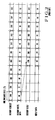
- Fig. 4 is a timing chart for explaining memory access in the second embodiment.
- Fig. 4 represents that the memory access for the channels (CH0 to CH3) is time-divisionally output during the 4T cycles, normally, and reply is returned during 4T cycles.
- DELT PTM - PTH is calculated, and the same operations as in the input operations can be performed until the PTM 16 is updated for reply.
- the flexibility with respect to a transfer speed can be improved, and a high-efficiency data transfer apparatus can be provided.
- the memory access buffer count is used, and the multiplexed memory access time slot corresponding to the channel is output. Therefore, a high efficient high-speed data transfer apparatus can be provided.
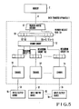
- Fig. 5 shows the third embodiment of the present invention.
- the same reference numerals in Fig. 5 denote the same parts as in Fig. 1.
- a data transfer apparatus 1 is connected to input/output devices 51 to 5n through connecting lines 31 to 3n, respectively.
- the data transfer apparatus 1 includes channels 111 to 11n to which channel numbers are respectively assigned, memory request flags 131 to 13n, set to be "1" during memory access, for controlling the memory access to a memory 2 in units of channels, a memory access decoder 61 for decoding the contents of the memory request flags 131 to 13n, measuring circuits 751 to 75n for measuring transfer speeds of the input/output devices 51 to 5n, and a change circuit 72 for changing the correspondence between the memory request flags 131 to 13n and the channel numbers on the basis of the measurement result of the measuring circuits 751 to 75n.
- the data transfer apparatus 1 performs a data transfer operation between the input/output devices 51 to 5n and the memory 2.
- the measuring circuits 751 to 75n respectively consist of 4-bit flip-flops (F/Fs), for holding the access counts between the channels and the input/output devices during one memory access cycle.
- an input/output instruction is output from a central processing unit (not shown) to the data transfer apparatus 1 of this embodiment, and a specific channel, e.g., the channel 112, starts the data transfer from/to the input/output device 52 using a connection path 32, and the data transfer from/to the memory 2 using the memory access flag 132.
- a specific channel e.g., the channel 112
- the change circuit 72 causes the memory request flag corresponding to the channel which does not perform memory access, e.g., the memory request flag 131, to correspond to the channel 112, thus performing the operation of the memory request.
- the change circuit 72 sequentially changes the correspondence between the memory request flag and the channel, and the memory access of the high-speed input/output device is preferentially processed.
- the memory request flag 132 is reset.
- a predetermined value is subtracted in the measuring circuit 752, and the measuring circuit 752 is completely reset when the memory request flag 131 is reset.
- the high-speed input/output device can perform multiplexed memory access corresponding to a multiple of the predetermined value of the measuring circuit, high-speed memory access can be expected.
- the data transfer apparatus including a plurality of memory request flags
- hardware can be decreased, thus providing a highly efficient data transfer apparatus.
Abstract
Description
- The present invention relates to a data transfer apparatus for a data processing system.
- A conventional data transfer apparatus of this type includes a plurality of memory access flags used to perform memory access. Each memory access is assigned to the corresponding channel. As shown in Fig. 2, a memory access time slot of one channel is assigned to a specific machine cycle of one period at the time of memory access. For example, in the memory access, data having a specific data length, e.g., 8-byte data, is exchanged between a memory and an input/output device within a predetermined period, e.g., four machine cycles each assigned to four channels. A memory access buffer is arranged for only one memory access cycle corresponding to, e.g., 8-byte data.
- In such a data transfer apparatus, an upper limit of memory access performance of one channel is determined. It is generally considered that the memory access speed is high, and is not lower than a transfer speed of an input/output device.
- However, an input/output device such as a semiconductor disk has been developed, and generations of a main frame and a peripheral system apparatus do not coincide with each other. Therefore, an input/output device having a transfer speed higher than the memory access speed has been required.
- In such a case, speed matching is performed between the input/output device and the data transfer apparatus through an adapter such as a local memory for buffering one block of a data record of the input/output device. However, this speed matching causes an increase in hardware, and a delay of an I/O time period occurs by an access time of the local memory. Therefore, the high-performance input/output device cannot be efficiently used.
- It is a principal object of the present invention to perform a data transfer operation more efficiently than a conventional apparatus.
- It is another object of the present invention to perform a data transfer operation at a higher speed than a conventional apparatus.
- In order to achieve the above object, according to the present invention, there is provided a data transfer apparatus comprising a plurality of channels which are respectively connected to input/output devices and to which channel numbers are respectively assigned, and transfer speed control means arranged between these channels and a memory, the transfer speed control means including means for monitoring a rate of data transfer from the input/output devices to the memory, and means for controlling and decreasing a difference in speed between data sent from the input/output devices and memory access when the monitor result represents a predetermined difference.
-
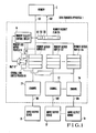
- Fig. 1 is a block diagram showing an arrangement of a data processing system which includes a data transfer apparatus according to the first embodiment of the present invention;
- Fig. 2 is a timing chart for explaining an operation of a conventional data transfer apparatus;
- Fig. 3 is a block diagram showing an arrangement of a data transfer apparatus according to the second embodiment of the present invention;
- Fig. 4 is a timing chart for explaining an operation of the data transfer apparatus according to the second embodiment of the present invention; and
- Fig. 5 is a block diagram showing an arrangement of a data transfer apparatus according to the third embodiment of the present invention.
- Preferred embodiments of the present invention will be described hereinafter with reference to the accompanying drawings.
- Referring to Fig. 1, a
data transfer apparatus 1 according to the first embodiment of the present invention is connected to input/output devices 31 to 3n through connectinglines 501 to 50n, respectively. This data transfer apparatus includeschannels 111 to 11n to which channel numbers are respectively assigned, memory request flags (MRF) 131 to 13n for controlling memory access to amemory 2 in units of the channels, a plurality ofmemory access buffers 121 to 12n (4W x 8B) which correspond to the channels and are used to perform memory access to thememory 2, a memory-side buffer pointer (PTM) 16 for counting the access count between thememory 2 and thebuffers 121 to 12n, a channel-side buffer pointer (PTH) 15 for counting the access count between thechannels 111 to 11n and thebuffers 121 to 12n, an arithmetic circuit (DELT) 17 for calculating a difference between the content of the memory-side buffer pointer 16 and that of the channel-side buffer pointer 15 to output a difference signal representing this difference, and a memoryrequest control circuit 14 for changing a correspondence between each memory request flag and the corresponding channel number when the difference signal exceeds a predetermined value. The data transfer apparatus performs data transfer between the input/output devices 31 to 3n and thememory 2. - When the input/
output device 32 receives an input/output instruction to perform data transfer, first, thepointers PTM 16 andPTH 15 are reset, and an output from theDELT 17 is set at "0". - Assume that the
PTH 15 is "+1" when 8-byte data is transferred from thechannel 112 to thebuffer 122. Since an input operation is performed, an output from theDELT 17 corresponds to PTH - PTM, i.e., goes to "1". Thecontrol circuit 14 turns thememory request flag 132 on, and starts memory access to store the 8-byte data in thememory 2. When the end condition of this memory request is returned from thememory 2, thePTM 16 is incremented by one, and an output from the DELT 17 returns to "0" again. - When the next 8-byte data is transferred from the input/
output device 32 to increment thePTH 15 by one, thePTH 15 goes to "2". When 8-byte data is fetched again from the channel to thebuffer 122 during memory access of thememory request flag 132 = "1", DELT = 2 since PTH = 3, and PTM = 1. Thecontrol circuit 14 determines from an output of the DELT = 2 that the transfer speed of the input/output device 32 is higher than the memory access speed, and assigns the memory request flag corresponding to the channel number which is not used, e.g., assigns thememory request flag 131 to thechannel 112, thus starting memory access. - Thus, when memory access is performed at a lower speed than that of the input/output device, a multiplexed memory request which can be stored in the
buffer 122 can be output. More specifically, since the buffer in this embodiment can store four words, the multiplexed memory request can be output up to a difference between the PTH and PTM, i.e., DELT = 4. - when the memory request end condition is returned, the
DELT 17 is sequentially decremented, and various memory access modes can be performed in accordance with a transfer speed of the input/output device. - Note that although the above description can be applied to an input operation, an output operation can be performed completely in the same manner as in the above description when an output from the
DELT 17 is PTM - PTH,. - The second embodiment of the present invention is shown in Fig. 3. The second embodiment has the same arrangement as in the first embodiment except for the following arrangement. In the second embodiment, a memory request
timing control circuit 24 is used in place of the memoryrequest control circuit 14 in Fig. 4 to change a timing of memory access when a difference signal exceeds a predetermined value, and memory access slot flip-flops (MAF) 231 to 23n are used in place of thememory request flags 131 to 13n. - Fig. 4 is a timing chart for explaining memory access in the second embodiment. Fig. 4 represents that the memory access for the channels (CH0 to CH3) is time-divisionally output during the 4T cycles, normally, and reply is returned during 4T cycles.
- When an input/
output device 31 is started in response to an input/output instruction, aPTM 16 and aPTH 15 are reset, and aDELT 17 goes to "0". In an input operation, since DELT = PTH - PTM. Therefore, when 8B data is transferred from achannel 111 to abuffer 121, PTH = 1, and DELT = 1. At this time, if anMAF 231 is set at "1", memory access can be performed. Therefore, memory access is performed, and the PTM is incremented by one in the next cycle, thus returning to DELT = 0. When the transfer speed of the input/output device 31 is high, and the next 8B data are continuously supplied from thechannel 111, as shown in Fig. 4, DELT = 2 may often be obtained. - At this time, the
timing control circuit 24 keeps theMAF 231 on during 2T cycles to skip the succeeding memory access slot of the CH1 (MAF1). Therefore, the memory access of the channel 111 (CHO) is continuously performed during the 2T cycles, and hence thePTM 16 is continuously incremented by one, thus returning to DELT = 0. - Thus, since the access cycles of the channel which requires high-speed memory access are time-divisionally multiplexed, in this embodiment, one channel access cycle can be performed by a maximum of a 4W buffer capacity, i.e., by DELT = 4.
- All the above operations are input operations. In an output operation, DELT = PTM - PTH is calculated, and the same operations as in the input operations can be performed until the
PTM 16 is updated for reply. - As described above, according to this embodiment, when the channel number correspondence of the memory request flag is changed, and the multiplexed memory request is supplied by the data count in the buffer, the flexibility with respect to a transfer speed can be improved, and a high-efficiency data transfer apparatus can be provided. According to this embodiment, in a data transfer apparatus for performing time-divisional memory access in correspondence with the channels, the memory access buffer count is used, and the multiplexed memory access time slot corresponding to the channel is output. Therefore, a high efficient high-speed data transfer apparatus can be provided.
- Fig. 5 shows the third embodiment of the present invention. The same reference numerals in Fig. 5 denote the same parts as in Fig. 1. Referring to Fig. 5, a
data transfer apparatus 1 is connected to input/output devices 51 to 5n through connectinglines 31 to 3n, respectively. Thedata transfer apparatus 1 includeschannels 111 to 11n to which channel numbers are respectively assigned,memory request flags 131 to 13n, set to be "1" during memory access, for controlling the memory access to amemory 2 in units of channels, amemory access decoder 61 for decoding the contents of thememory request flags 131 to 13n, measuringcircuits 751 to 75n for measuring transfer speeds of the input/output devices 51 to 5n, and achange circuit 72 for changing the correspondence between thememory request flags 131 to 13n and the channel numbers on the basis of the measurement result of themeasuring circuits 751 to 75n. Thedata transfer apparatus 1 performs a data transfer operation between the input/output devices 51 to 5n and thememory 2. Themeasuring circuits 751 to 75n respectively consist of 4-bit flip-flops (F/Fs), for holding the access counts between the channels and the input/output devices during one memory access cycle. - Assume that an input/output instruction is output from a central processing unit (not shown) to the
data transfer apparatus 1 of this embodiment, and a specific channel, e.g., thechannel 112, starts the data transfer from/to the input/output device 52 using aconnection path 32, and the data transfer from/to thememory 2 using thememory access flag 132. - When the transfer speed of the input/
output device 52 is high, and the access count between the channel and the input/output device which exceeds the predetermined value (when a difference occurs with respect to the predetermined value) is measured by the measuringcircuit 752 while thememory request flag 132 is ON, thechange circuit 72 causes the memory request flag corresponding to the channel which does not perform memory access, e.g., thememory request flag 131, to correspond to thechannel 112, thus performing the operation of the memory request. At this time, if thechannel 111 starts memory access, thechange circuit 72 sequentially changes the correspondence between the memory request flag and the channel, and the memory access of the high-speed input/output device is preferentially processed. - When the preceding memory access is completed, the
memory request flag 132 is reset. At the same time, a predetermined value is subtracted in the measuringcircuit 752, and the measuringcircuit 752 is completely reset when thememory request flag 131 is reset. - Thus, since the high-speed input/output device can perform multiplexed memory access corresponding to a multiple of the predetermined value of the measuring circuit, high-speed memory access can be expected.
- As described above, according to the present invention, in the data transfer apparatus including a plurality of memory request flags, when a plurality of memory request flags are assigned to perform memory access of the high-speed input/output device, hardware can be decreased, thus providing a highly efficient data transfer apparatus.
Claims (4)
a plurality of channels which are respectively connected to input/output devices and to which channel numbers are respectively assigned; and
transfer speed control means arranged between said channels and a memory;
said transfer speed control means including means for monitoring a rate of data transfer from said input/output devices to said memory; and
means for controlling and decreasing a difference in speed between data sent from said input/output devices and memory access when the monitor result represents a predetermined difference.
said monitoring means includes a plurality of memory request flags for controlling memory access to said memory in units of said channels, a memory-side buffer pointer for counting an access count between said memory and said memory access buffers, and a channel-side buffer pointer for counting an access count between said channels and said memory access buffers; and
said control means further includes an arithmetic circuit for calculating a difference between the content of said memory-side buffer pointer and that of said channel-side buffer pointer to output a difference signal, and changing means for changing a correspondence between said memory request flags and the channel numbers when the difference signal exceeds a predetermined value, said changing means assigning said plurality of memory request flags when the difference signal exceeds the predetermined value.
said monitoring means includes a plurality of memory access slot flip-flops for controlling a memory access time slot of said memory in units of channels, a memory-side buffer pointer for counting an access count between said memory and said memory access buffers, and a channel-side buffer pointer for counting an access count between said channels and said memory access buffers; and
said control means further includes an arithmetic circuit for calculating a difference between the content of said memory-side buffer pointer and that of said channel-side buffer pointer to output a difference signal, and changing means for changing a memory access timing when the difference signal exceeds a predetermined value, said changing means multiplexing the memory access time slots when the difference signal exceeds the predetermined value.
said controlling means includes changing means for changing a correspondence between said memory request flags and the channel numbers on the basis of the measurement result of said measuring means, said plurality of memory request flags being used to achieve high-speed memory access when a transfer speed of said input/output device increases upon generation of the difference with respect to a predetermined value.
Applications Claiming Priority (6)
| Application Number | Priority Date | Filing Date | Title |
|---|---|---|---|
| JP63318428A JP2669020B2 (en) | 1988-12-19 | 1988-12-19 | Data transfer device |
| JP31842988A JPH0715669B2 (en) | 1988-12-19 | 1988-12-19 | Data transfer device |
| JP318429/88 | 1988-12-19 | ||
| JP31842888 | 1988-12-19 | ||
| JP318428/88 | 1988-12-19 | ||
| JP31842988 | 1988-12-19 |
Publications (3)
| Publication Number | Publication Date |
|---|---|
| EP0374764A2 true EP0374764A2 (en) | 1990-06-27 |
| EP0374764A3 EP0374764A3 (en) | 1992-11-19 |
| EP0374764B1 EP0374764B1 (en) | 2001-04-04 |
Family
ID=26569363
Family Applications (1)
| Application Number | Title | Priority Date | Filing Date |
|---|---|---|---|
| EP89123261A Expired - Lifetime EP0374764B1 (en) | 1988-12-19 | 1989-12-15 | Data transfer apparatus |
Country Status (3)
| Country | Link |
|---|---|
| US (1) | US5414816A (en) |
| EP (1) | EP0374764B1 (en) |
| DE (1) | DE68929288T2 (en) |
Cited By (3)
| Publication number | Priority date | Publication date | Assignee | Title |
|---|---|---|---|---|
| WO2015160496A1 (en) * | 2014-04-16 | 2015-10-22 | Sandisk Technologies Inc. | Storage module and method for adaptive burst mode |
| US9569352B2 (en) | 2013-03-14 | 2017-02-14 | Sandisk Technologies Llc | Storage module and method for regulating garbage collection operations based on write activity of a host |
| US9990158B2 (en) | 2016-06-22 | 2018-06-05 | Sandisk Technologies Llc | Storage system and method for burst mode management using transfer RAM |
Families Citing this family (16)
| Publication number | Priority date | Publication date | Assignee | Title |
|---|---|---|---|---|
| US5878280A (en) * | 1993-09-23 | 1999-03-02 | Philips Electronics North America Corp. | Data buffering system for plural data memory arrays |
| JPH07210500A (en) * | 1994-01-25 | 1995-08-11 | Fujitsu Ltd | Data transfer controller |
| JP3174211B2 (en) * | 1994-01-25 | 2001-06-11 | 富士通株式会社 | Move-in control method for buffer storage |
| US5701514A (en) * | 1994-04-01 | 1997-12-23 | International Business Machines Corporation | System providing user definable selection of different data transmission modes of drivers of an I/O controller transmitting to peripherals with different data transmission rate |
| US5991835A (en) * | 1994-11-22 | 1999-11-23 | Teac Corporation | Peripheral data storage device in which time interval used for data transfer from relatively fast buffer memory to relatively slower main memory is selected in view of average of time intervals during which data blocks were recently received from host |
| US5570381A (en) * | 1995-04-28 | 1996-10-29 | Mosaid Technologies Incorporated | Synchronous DRAM tester |
| US5659799A (en) * | 1995-10-11 | 1997-08-19 | Creative Technology, Ltd. | System for controlling disk drive by varying disk rotation speed when buffered data is above high or below low threshold for predetermined damping period |
| US5819053A (en) * | 1996-06-05 | 1998-10-06 | Compaq Computer Corporation | Computer system bus performance monitoring |
| US6038621A (en) * | 1996-11-04 | 2000-03-14 | Hewlett-Packard Company | Dynamic peripheral control of I/O buffers in peripherals with modular I/O |
| US6407983B1 (en) * | 1998-02-20 | 2002-06-18 | Adc Telecommunications, Inc. | Circuit and method for shaping traffic in a virtual connection network |
| US6408348B1 (en) | 1999-08-20 | 2002-06-18 | International Business Machines Corporation | System, method, and program for managing I/O requests to a storage device |
| US20020062415A1 (en) * | 2000-09-29 | 2002-05-23 | Zarlink Semiconductor N.V. Inc. | Slotted memory access method |
| US9703527B2 (en) * | 2012-12-31 | 2017-07-11 | Sandisk Technologies Llc | Storage device and method for reallocating storage device resources based on an estimated fill level of a host buffer |
| US8938561B2 (en) * | 2013-01-10 | 2015-01-20 | Skymedi Corporation | Time-sharing buffer access system |
| US9875128B2 (en) * | 2015-01-23 | 2018-01-23 | Red Hat Israel, Ltd. | Using hypervisor trapping for protection against interrupts in virtual machine functions |
| WO2020117481A1 (en) * | 2018-12-04 | 2020-06-11 | Rambus Inc. | Off-module data buffer |
Citations (2)
| Publication number | Priority date | Publication date | Assignee | Title |
|---|---|---|---|---|
| US4171536A (en) * | 1976-05-03 | 1979-10-16 | International Business Machines Corporation | Microprocessor system |
| JPS58223861A (en) * | 1982-06-23 | 1983-12-26 | Nippon Telegr & Teleph Corp <Ntt> | Data double recording system of input and output controller |
Family Cites Families (24)
| Publication number | Priority date | Publication date | Assignee | Title |
|---|---|---|---|---|
| US3516090A (en) * | 1965-05-21 | 1970-06-02 | Gen Electric | Current limiting circuit breaker with independent acting high speed opening means |
| US3639909A (en) * | 1970-01-26 | 1972-02-01 | Burroughs Corp | Multichannel input/output control with automatic channel selection |
| IL40597A (en) * | 1971-11-11 | 1976-06-30 | Ciba Geigy Ag | Anti-hypertensively active pharmaceutical preparations containing an anti-hypertensively active amino acid and a beta-hydroxylase inhibitor |
| JPS6055848B2 (en) * | 1975-10-15 | 1985-12-06 | 株式会社東芝 | information processing equipment |
| US4400771A (en) * | 1975-12-04 | 1983-08-23 | Tokyo Shibaura Electric Co., Ltd. | Multi-processor system with programmable memory-access priority control |
| US4130864A (en) * | 1976-10-29 | 1978-12-19 | Westinghouse Electric Corp. | Priority selection circuit for multiported central functional unit with automatic priority reduction on excessive port request |
| US4258418A (en) * | 1978-12-28 | 1981-03-24 | International Business Machines Corporation | Variable capacity data buffer system |
| US4423482A (en) * | 1981-06-01 | 1983-12-27 | Sperry Corporation | FIFO Register with independent clocking means |
| US4644463A (en) * | 1982-12-07 | 1987-02-17 | Burroughs Corporation | System for regulating data transfer operations |
| US4571671A (en) * | 1983-05-13 | 1986-02-18 | International Business Machines Corporation | Data processor having multiple-buffer adapter between a system channel and an input/output bus |
| US4591973A (en) * | 1983-06-06 | 1986-05-27 | Sperry Corporation | Input/output system and method for digital computers |
| US4642797A (en) * | 1983-11-10 | 1987-02-10 | Monolithic Memories, Inc. | High speed first-in-first-out memory |
| CA1228677A (en) * | 1984-06-21 | 1987-10-27 | Cray Research, Inc. | Peripheral interface system |
| JPH0816891B2 (en) * | 1985-10-01 | 1996-02-21 | 株式会社日立製作所 | Channel system |
| JPS62138948A (en) * | 1985-12-13 | 1987-06-22 | Hitachi Ltd | Data transferring equipment |
| JPS62208153A (en) * | 1986-03-08 | 1987-09-12 | Nec Corp | Input/output buffer device |
| US4860193A (en) * | 1986-05-22 | 1989-08-22 | International Business Machines Corporation | System for efficiently transferring data between a high speed channel and a low speed I/O device |
| JPS62297963A (en) * | 1986-06-18 | 1987-12-25 | Fujitsu Ltd | Allocating circuit for time slot |
| US4805094A (en) * | 1986-08-27 | 1989-02-14 | American Telephone & Telegraph Company | Multi-channel memory access circuit |
| US4831523A (en) * | 1986-10-31 | 1989-05-16 | Bull Hn Information Systems Inc. | Multiple DMA controller chip sequencer |
| US4821170A (en) * | 1987-04-17 | 1989-04-11 | Tandem Computers Incorporated | Input/output system for multiprocessors |
| US4991084A (en) * | 1988-02-05 | 1991-02-05 | International Business Machines Corporation | N×M round robin order arbitrating switching matrix system |
| JP2562473B2 (en) * | 1988-02-19 | 1996-12-11 | 株式会社日立製作所 | Data writing control method for magnetic tape subsystem |
| CA1331801C (en) * | 1988-03-17 | 1994-08-30 | Yasuro Shobatake | Packet switching device |
-
1989
- 1989-12-15 EP EP89123261A patent/EP0374764B1/en not_active Expired - Lifetime
- 1989-12-15 DE DE68929288T patent/DE68929288T2/en not_active Expired - Fee Related
-
1993
- 1993-09-03 US US08/115,754 patent/US5414816A/en not_active Expired - Lifetime
Patent Citations (2)
| Publication number | Priority date | Publication date | Assignee | Title |
|---|---|---|---|---|
| US4171536A (en) * | 1976-05-03 | 1979-10-16 | International Business Machines Corporation | Microprocessor system |
| JPS58223861A (en) * | 1982-06-23 | 1983-12-26 | Nippon Telegr & Teleph Corp <Ntt> | Data double recording system of input and output controller |
Non-Patent Citations (2)
| Title |
|---|
| PATENT ABSTRACTS OF JAPAN vol. 12, no. 192 (P-712)(3039) 4 June 1988 * |
| PATENT ABSTRACTS OF JAPAN vol. 8, no. 82 (P-268)(1519) 14 April 1984 & JP-A-58 223 861 ( NIPPON DENSHIN ) 26 December 1983 * |
Cited By (4)
| Publication number | Priority date | Publication date | Assignee | Title |
|---|---|---|---|---|
| US9569352B2 (en) | 2013-03-14 | 2017-02-14 | Sandisk Technologies Llc | Storage module and method for regulating garbage collection operations based on write activity of a host |
| WO2015160496A1 (en) * | 2014-04-16 | 2015-10-22 | Sandisk Technologies Inc. | Storage module and method for adaptive burst mode |
| US9471254B2 (en) | 2014-04-16 | 2016-10-18 | Sandisk Technologies Llc | Storage module and method for adaptive burst mode |
| US9990158B2 (en) | 2016-06-22 | 2018-06-05 | Sandisk Technologies Llc | Storage system and method for burst mode management using transfer RAM |
Also Published As
| Publication number | Publication date |
|---|---|
| US5414816A (en) | 1995-05-09 |
| DE68929288D1 (en) | 2001-05-10 |
| DE68929288T2 (en) | 2001-11-15 |
| EP0374764B1 (en) | 2001-04-04 |
| EP0374764A3 (en) | 1992-11-19 |
Similar Documents
| Publication | Publication Date | Title |
|---|---|---|
| EP0374764B1 (en) | Data transfer apparatus | |
| JP2611746B2 (en) | Input / output interface device and control method thereof | |
| US4598363A (en) | Adaptive delayed polling of sensors | |
| US4543626A (en) | Apparatus and method for controlling digital data processing system employing multiple processors | |
| US4654632A (en) | Analog-to-digital converter | |
| US5696940A (en) | Apparatus and method for sharing first-in first-out memory space between two streams of data | |
| US4658349A (en) | Direct memory access control circuit and data processing system using said circuit | |
| US4742446A (en) | Computer system using cache buffer storage unit and independent storage buffer device for store through operation | |
| KR0155368B1 (en) | Ram based event counter method and apparatus | |
| EP0420236A2 (en) | Arrangement and method of controlling memory access requests in digital data processing system | |
| GB2085624A (en) | A coupling equipment for the control of access of data processors to a data line | |
| US5944788A (en) | Message transfer system and control method for multiple sending and receiving modules in a network supporting hardware and software emulated modules | |
| US5999969A (en) | Interrupt handling system for message transfers in network having mixed hardware and software emulated modules | |
| EP0099462A2 (en) | Apparatus and method for buffering data in a data processing system | |
| US5983266A (en) | Control method for message communication in network supporting software emulated modules and hardware implemented modules | |
| JP2669020B2 (en) | Data transfer device | |
| US5842003A (en) | Auxiliary message arbitrator for digital message transfer system in network of hardware modules | |
| EP0299264A2 (en) | A byte queing/dequeuing apparatus for handling variable-length data words/instructions in a single clock cycle | |
| JP2688245B2 (en) | DMA controller | |
| JPH0833869B2 (en) | Data processing device | |
| JPH08249273A (en) | Asynchronous transfer circuit with transfer speed switching function | |
| JPS6224830B2 (en) | ||
| KR950008395B1 (en) | Data transferring apparatus between mimd processor and host computer | |
| JPS58189719A (en) | Data transfer control system | |
| SU717769A1 (en) | Device for control of interruption of programs |
Legal Events
| Date | Code | Title | Description |
|---|---|---|---|
| PUAI | Public reference made under article 153(3) epc to a published international application that has entered the european phase |
Free format text: ORIGINAL CODE: 0009012 |
|
| 17P | Request for examination filed |
Effective date: 19900110 |
|
| AK | Designated contracting states |
Kind code of ref document: A2 Designated state(s): BE DE FR GB IT NL |
|
| PUAL | Search report despatched |
Free format text: ORIGINAL CODE: 0009013 |
|
| AK | Designated contracting states |
Kind code of ref document: A3 Designated state(s): BE DE FR GB IT NL |
|
| 17Q | First examination report despatched |
Effective date: 19940607 |
|
| GRAG | Despatch of communication of intention to grant |
Free format text: ORIGINAL CODE: EPIDOS AGRA |
|
| 17Q | First examination report despatched |
Effective date: 19940607 |
|
| GRAG | Despatch of communication of intention to grant |
Free format text: ORIGINAL CODE: EPIDOS AGRA |
|
| GRAH | Despatch of communication of intention to grant a patent |
Free format text: ORIGINAL CODE: EPIDOS IGRA |
|
| GRAH | Despatch of communication of intention to grant a patent |
Free format text: ORIGINAL CODE: EPIDOS IGRA |
|
| RAP1 | Party data changed (applicant data changed or rights of an application transferred) |
Owner name: NEC CORPORATION |
|
| GRAA | (expected) grant |
Free format text: ORIGINAL CODE: 0009210 |
|
| AK | Designated contracting states |
Kind code of ref document: B1 Designated state(s): BE DE FR GB IT NL |
|
| REF | Corresponds to: |
Ref document number: 68929288 Country of ref document: DE Date of ref document: 20010510 |
|
| ITF | It: translation for a ep patent filed |
Owner name: MODIANO & ASSOCIATI S.R.L. |
|
| ET | Fr: translation filed | ||
| RAP2 | Party data changed (patent owner data changed or rights of a patent transferred) |
Owner name: NEC CORPORATION |
|
| NLT2 | Nl: modifications (of names), taken from the european patent patent bulletin |
Owner name: NEC CORPORATION |
|
| REG | Reference to a national code |
Ref country code: GB Ref legal event code: IF02 |
|
| PLBE | No opposition filed within time limit |
Free format text: ORIGINAL CODE: 0009261 |
|
| STAA | Information on the status of an ep patent application or granted ep patent |
Free format text: STATUS: NO OPPOSITION FILED WITHIN TIME LIMIT |
|
| 26N | No opposition filed | ||
| PGFP | Annual fee paid to national office [announced via postgrant information from national office to epo] |
Ref country code: DE Payment date: 20061207 Year of fee payment: 18 |
|
| PGFP | Annual fee paid to national office [announced via postgrant information from national office to epo] |
Ref country code: FR Payment date: 20061208 Year of fee payment: 18 |
|
| PGFP | Annual fee paid to national office [announced via postgrant information from national office to epo] |
Ref country code: GB Payment date: 20061213 Year of fee payment: 18 |
|
| PGFP | Annual fee paid to national office [announced via postgrant information from national office to epo] |
Ref country code: NL Payment date: 20061217 Year of fee payment: 18 |
|
| PGFP | Annual fee paid to national office [announced via postgrant information from national office to epo] |
Ref country code: IT Payment date: 20061231 Year of fee payment: 18 |
|
| PGFP | Annual fee paid to national office [announced via postgrant information from national office to epo] |
Ref country code: BE Payment date: 20070222 Year of fee payment: 18 |
|
| BERE | Be: lapsed |
Owner name: *NEC CORP. Effective date: 20071231 |
|
| GBPC | Gb: european patent ceased through non-payment of renewal fee |
Effective date: 20071215 |
|
| NLV4 | Nl: lapsed or anulled due to non-payment of the annual fee |
Effective date: 20080701 |
|
| PG25 | Lapsed in a contracting state [announced via postgrant information from national office to epo] |
Ref country code: BE Free format text: LAPSE BECAUSE OF NON-PAYMENT OF DUE FEES Effective date: 20071231 |
|
| PG25 | Lapsed in a contracting state [announced via postgrant information from national office to epo] |
Ref country code: DE Free format text: LAPSE BECAUSE OF NON-PAYMENT OF DUE FEES Effective date: 20080701 |
|
| REG | Reference to a national code |
Ref country code: FR Ref legal event code: ST Effective date: 20081020 |
|
| PG25 | Lapsed in a contracting state [announced via postgrant information from national office to epo] |
Ref country code: NL Free format text: LAPSE BECAUSE OF NON-PAYMENT OF DUE FEES Effective date: 20080701 |
|
| PG25 | Lapsed in a contracting state [announced via postgrant information from national office to epo] |
Ref country code: GB Free format text: LAPSE BECAUSE OF NON-PAYMENT OF DUE FEES Effective date: 20071215 |
|
| PG25 | Lapsed in a contracting state [announced via postgrant information from national office to epo] |
Ref country code: FR Free format text: LAPSE BECAUSE OF NON-PAYMENT OF DUE FEES Effective date: 20071231 |
|
| PG25 | Lapsed in a contracting state [announced via postgrant information from national office to epo] |
Ref country code: IT Free format text: LAPSE BECAUSE OF NON-PAYMENT OF DUE FEES Effective date: 20071215 |