EP0378894A2 - Fabrication of GaAs integrated circuits - Google Patents
Fabrication of GaAs integrated circuits Download PDFInfo
- Publication number
- EP0378894A2 EP0378894A2 EP89308623A EP89308623A EP0378894A2 EP 0378894 A2 EP0378894 A2 EP 0378894A2 EP 89308623 A EP89308623 A EP 89308623A EP 89308623 A EP89308623 A EP 89308623A EP 0378894 A2 EP0378894 A2 EP 0378894A2
- Authority
- EP
- European Patent Office
- Prior art keywords
- layer
- compound semiconductor
- bandgap energy
- cap
- photoresist
- Prior art date
- Legal status (The legal status is an assumption and is not a legal conclusion. Google has not performed a legal analysis and makes no representation as to the accuracy of the status listed.)
- Withdrawn
Links
Images


Classifications
-
- H—ELECTRICITY
- H01—ELECTRIC ELEMENTS
- H01L—SEMICONDUCTOR DEVICES NOT COVERED BY CLASS H10
- H01L21/00—Processes or apparatus adapted for the manufacture or treatment of semiconductor or solid state devices or of parts thereof
- H01L21/70—Manufacture or treatment of devices consisting of a plurality of solid state components formed in or on a common substrate or of parts thereof; Manufacture of integrated circuit devices or of parts thereof
- H01L21/71—Manufacture of specific parts of devices defined in group H01L21/70
- H01L21/76—Making of isolation regions between components
- H01L21/7605—Making of isolation regions between components between components manufactured in an active substrate comprising AIII BV compounds
-
- H—ELECTRICITY
- H01—ELECTRIC ELEMENTS
- H01L—SEMICONDUCTOR DEVICES NOT COVERED BY CLASS H10
- H01L21/00—Processes or apparatus adapted for the manufacture or treatment of semiconductor or solid state devices or of parts thereof
- H01L21/70—Manufacture or treatment of devices consisting of a plurality of solid state components formed in or on a common substrate or of parts thereof; Manufacture of integrated circuit devices or of parts thereof
- H01L21/77—Manufacture or treatment of devices consisting of a plurality of solid state components or integrated circuits formed in, or on, a common substrate
- H01L21/78—Manufacture or treatment of devices consisting of a plurality of solid state components or integrated circuits formed in, or on, a common substrate with subsequent division of the substrate into plural individual devices
- H01L21/82—Manufacture or treatment of devices consisting of a plurality of solid state components or integrated circuits formed in, or on, a common substrate with subsequent division of the substrate into plural individual devices to produce devices, e.g. integrated circuits, each consisting of a plurality of components
- H01L21/8252—Manufacture or treatment of devices consisting of a plurality of solid state components or integrated circuits formed in, or on, a common substrate with subsequent division of the substrate into plural individual devices to produce devices, e.g. integrated circuits, each consisting of a plurality of components the substrate being a semiconductor, using III-V technology
-
- Y—GENERAL TAGGING OF NEW TECHNOLOGICAL DEVELOPMENTS; GENERAL TAGGING OF CROSS-SECTIONAL TECHNOLOGIES SPANNING OVER SEVERAL SECTIONS OF THE IPC; TECHNICAL SUBJECTS COVERED BY FORMER USPC CROSS-REFERENCE ART COLLECTIONS [XRACs] AND DIGESTS
- Y10—TECHNICAL SUBJECTS COVERED BY FORMER USPC
- Y10S—TECHNICAL SUBJECTS COVERED BY FORMER USPC CROSS-REFERENCE ART COLLECTIONS [XRACs] AND DIGESTS
- Y10S148/00—Metal treatment
- Y10S148/072—Heterojunctions
Definitions
- a selectively doped heterostructure transistor, SDHT (also known as a MODFET for modulation doped FET, a TEGFET for two-dimensional electron gas FET, or a HEMT for high electron mobility transistor, and will be referred to generically, for purposes here, as a heterojunction field effect transistor, or HFET) has supeprior performance compared to conventional (non-heterojunction) metal-semiconductor FETs (MESFET) in bandwidth and noise figure, etc.
- MESFET metal-semiconductor FETs
- One drawback to using HFETs is the difficulty in the formation thereof in integrated form with consistent device characteristics across a wafer, even across a single chip. For example, the threshold voltage of HFETs can vary so much in a single chip that logic circuits built using HFETs do not operate reliably, reducing the yield of operable circuits from a wafer.
- a new process has been invented for the manufacture of both enhancement and depletion HFETs in integrated form with consistent threshold voltages across a wafer and a self-aligned structure.
- these advantages have been achieved generally by growing a buffer layer of compound semiconductor material with a first bandgap energy; growing a first spacer layer of compound semiconductor material with a second bandgap energy, growing a donor layer of doped compound semiconductor material with the second bandgap energy; growing a first cap layer of compound semiconductor material with the first bandgap energy; growing an etch-stop layer of compound semiconductor material with a third bandgap energy; and, growing a second cap layer of compound semiconductor material with the first bandgap energy.
- the second and third bandgap energies are more than the first bandgap energy.
- the layers are preferably grown by a molecular beam epitaxy process to achieve precise control over the thicknesses of the layers.
- a further embodiment which generally achieves the above advantages and utilizes the epitaxial layer formed by the layers discussed above, involves isolating selected regions of the epitaxial layer; etching portions of the selected regions of the epitaxial layer to a predetermined depth where enhancement FETs are to be formed; forming gate electrodes for both enhancement and depletion FETs; forming source/drain regions for the drain and source electrodes of the enhancement and depletion FETs; contacting the source/drain regions, depositing a dielectric layer, selectively etching the dielectric for vias, forming an interconnect layer; and passivating the resulting structure.
- the steps of depositing a dielectric layer, selectively etching the dielectric layer for vias and forming an interconnect layer may be repeated for each desired layer of interconnect.
- the precise control over the thickness of the layers and the precision etching thereof ensures uniformity in the threshold voltages of the HFETs.
- the etch-stop layer allows for precision etching of the wafer where enhancement HFETs are to be formed.
- the resulting HFET structures are substantially planar, allowing for reliable metalization of the wafer.
- the method of isolating devices on the wafer is achieved generally by selectively implanting isolation dopant onto the wafer a predetermined depth into the epitaxial layer where conductivity therein is to be reduced; annealing the wafer at a predetermined temperature; selectively implanting isolation dopant into the wafer completely through the epitaxial layer into the substrate; and annealing the wafer a second time at a temperature less than the predetermined temperature.
- the compound semiconductor material referred to here is based on gallium arsenide (GaAs) and aluminum gallium arsenide (AlGaAs), other compound semiconductor materials could be substituted, such as indium aluminum arsenide (InAlAs) and indium gallium arsenide (InGaAs), respectively.
- concentration (i.e., mole fraction) of aluminum in the AlGaAs is usually identified as x in Al x Ga 1-x As, where x can range from 0 (0%, or no aluminum) to 1 (100% aluminum, or no gallium), depending on the bandgap energy required of the material. Generally, the more the aluminum, the higher the bandgap energy of the AlGaAs material.
- gallium arsenide will be identified as GaAs and aluminum gallium arsenide will be identified as AlGaAs.
- the concentration of aluminum in AlGaAs will be designated by percentage of aluminum therein.
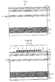
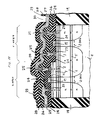
- FIG. 1 a partial cross-sectional view (not to scale) of a wafer 1 ready for the manufacturing of both enhancement and depletion selectively doped heterojunction field-effect transistors (hereinafter referred to as E-HFET and D-HFET, respectively) is shown.
- layers 3 through 11 are grown on a semi-insulating GaAs substrate 2 in a molecular beam epitaxy (MBE) machine, forming an essentially continuous layer from the substrate 2.
- MBE molecular beam epitaxy
- One such MBE machine capable of growing GaAs and AlGaAs layers is a Varian Gen II, manufactured by Varian Associates of Santa Clara, California.
- Layer 3 contains therein multiple alternating layers of GaAs and AlGaAs to form a superlattice which reduces the likelihood that impurities and defects will propagate from the substrate 2 into higher layers 4 through 10. This superlattice reduces the need for a thicker buffer layer 4, decreasing the time necessary for the growth of the epitaxial layer.
- Each of the alternating layers has a thickness less than an electron or hole wave function, e.g., 4 nanometers or less. Using an exemplary aluminum concentration of 22%, it has been found that ten alternating layers, or periods, is sufficient. This results in the overall thickness of the layer 3 of approximately 80 nanometers.
- a buffer layer 4 of undoped GaAs is deposited having a typical thickness range of approximately 10 to 1000 nanometers, preferably 300 nanometers.
- the buffer layer 4 supports a two-dimensional electron gas (2-DEG), which is the channel, or active region, of the E-HFETs and D-HFETs. It is in the channel that current flows between the drain and source electrodes of corresponding E-HFETs and D-HFETs.
- 2-DEG two-dimensional electron gas
- a first spacer layer 5 is deposited over the buffer layer 4, a donor layer 6 is deposited on the spacer layer 5, and a second spacer layer 7 is deposited over the donor layer.
- the first and second spacer and donor layers 5, 7, 6 are of AlGaAs.
- the donor layer 6 is doped, and as will be explained in more detail below, the doping concentration strongly influences the threshold voltages of the D-HFETs and E-HFETs. To assure full depletion of the donor layer 6 under zero bias conditions for an E-HFET, the donor layer should be less than 30 nanometers thick. Further, the acceptable uniform concentration of aluminum in the donor layer 6 and the spacer layers 5, 7 ranges from 10% to 60% and is preferably 22%.
- the dopant used is preferably silicon, but other dopants, such as selenium, could be used to make the conductivity of the layer 6 N-type.
- the same dopant is used for implants where N-type conductivity regions are desired in the wafer 1.
- the doping density in the donor layer 6, prior to a subsequent wafer anneal step ranges from 5x10¹⁷ to 2x10⁸ atoms cm ⁇ 3 and is preferably 6x10¹⁷ atoms cm ⁇ 3. Equivalently, beryllium, carbon or other suitable species could be used to make the conductivity of layer 6 P-type.
- the first spacer layer 5 enhances the electron mobility of the 2-DEG by confining the 2-DEG to the buffer layer 4, thereby reducing scattering of the 2-DEG by impurities in layers 5 and 6 and in the interface between layers 4 and 5, increasing the mobility 2-DEG.
- the second spacer layer 7, along with the first spacer layer 5, functions to absorb out-diffusion of dopant from the donor layer 6 during later high-temperature processing, such as annealing.
- the thickness of the spacer layer 5 is a trade-off between the transconductance of the desired E-HFET or D-HFET and the desired increase in mobility of the electrons in the 2-DEG, resulting in a thickness ranging from 1 to 5 nanometers, with approximately 2.5 nanometers as an acceptable compromise after a wafer annealing step, as discussed in more detail below.
- the thickness of the second spacer layer 7 is similar to that for the first spacer layer 5.
- the primary purpose of the second layer 7 is to absorb dopant from the donor layer 6 and prevent the dopant from reaching an upper layer and may have virtually no thickness after the anneal.
- the first spacer layer 5 must be thick enough to properly confine the 2-DEG to the buffer layer 4.
- the thickness of the second spacer layer 7 can be somewhat less than the thickness of the first spacer layer 5.
- First and second cap layers 8, 10 are undoped GaAs layers used for forming thereon Schottky barrier gate contacts and ohmic drain and source contacts for E-HFETs and D-HFETs, respectively, as will be discussed in more detail below.
- the cap layers 8, 10 are approximately 10 nanometers thick.
- the aluminum concentration in the etch-stop layer 9 ranges from 10% to 60% and is preferably 50%.
- a protective layer 11 of AlGaAs is deposited, having a aluminum concentration substantially the same as the etch-stop layer 9 and a thickness of about that of cap layers 8, 10. As will be described in more detail below, layer 11 is sacrificed to protect the wafer 1 from contamination or damage before a final etch and the deposition of metal to form the gates.
- the doping of the donor layer 6 and the distance the gates of the corresponding E-HFETs and D-HFETs are from the 2-DEG layer establishes the threshold voltages of the E-HFET and the D-HFETs.
- the corresponding distances are set by the thicknesses of the layers 5 - 10 for the D- HFETs and layers 5 - 8 for the E-HFETs. So critical are thickness of the layers 5 - 10 that for one tenth nanometer of error the threshold voltage of a D-HFET shifts approximately two to five millivolts and of an E-HFET shifts approximately two millivolts.
- the thicknesses of the layers 5 - 10 are calculated.
- the combined thickness of layers 5 - 8 is substantially 50 nanometers.
- the combined thickness of layers 5 - 10 is substantially 100 nanometers.
- the epitaxial layer includes the buffer layer 4, first and second spacer layers 5, 7, donor layer 6, first and second cap layers 8, 10 and the etch-stop layer 9.
- the superlattice structure 3 and the protective layer 11 are used advantageously in cooperation with the rest of the layers 4 - 10, but are not an indispensable portion of the claimed invention.
- the first and second spacer layers 5,7 can be deleted from wafer 1 when fabricating MESFET devices, mentioned above.
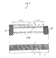
- a shallow isolation of selected regions of the wafer is made.
- a layer of photoresist 12 for example, Shipley AZ-1350J photoresist
- An implant source provides an isolation dopant 13, preferably ionized oxygen, which is driven into the wafer.
- Exemplary energy levels for the ionized oxygen range from 20 to 160 keV, with a dose of 5 ⁇ 1012 to 1.5 ⁇ 1014 oxygen ions cm ⁇ 2; the higher the energy, the deeper the implant.
- An exemplary implant is a dose of 1x10¹⁴ ions cm ⁇ 2 at 40 keV then at 125 keV.
- the resulting peak concentration of oxygen atoms in the wafer 1 ranges from 5 ⁇ 1018 to 1 ⁇ 1019 atoms cm ⁇ 3.
- the implanted oxygen destroys the conductivity of the wafer where exposed to the implant, thereby isolating and reducing capacitive loading on devices later formed in the wafer 1.
- the resulting isolation regions 14 are formed, as shown in FIG. 3.
- the photoresist layer 12 of FIG. 2 is then removed and another photoresist is deposited (not shown). This photoresist is patterned to expose the underlying wafer in regions of the wafer where E-HFETs are to be formed.
- the exposed protective layer 11 is then etched to the second cap layer 10 using an AlGaAs etchant described below.
- the second cap layer 10 is itself etched to expose the etch-stop layer 9.
- the photoresist (not shown) is then removed and the wafer thoroughly cleaned.
- the previously un-etched portion of protective layer 11 and the exposed etch-stop layer 9 are then simultaneously etched to expose the portions of the second cap layer 10 where D-HFETs are to be formed and the portions of the first cap layer 8 where E-HFETs are to be formed. This results in the structure substantially as shown in FIG. 3.
- the etching of the second cap layer 10 (GaAs) to the etch-stop layer 9 is preferably by a wet etch of the wafer in a conventional potassium iodide/iodine (KI/I2) solution until the GaAs is removed. Alternatively, a reactive ion etch could be used. Although the etch is selective, the over-etching of the GaAs second cap layer 10 into the AlGaAs etch-stop layer 9 is not critical. Advantageously, the over-etching of second cap layer 10 into the etch-stop layer 9 ensures complete removal of the second cap layer 10, resulting in a more uniform etch of etch-stop layer 9.
- KI/I2 potassium iodide/iodine
- the etching of the AlGaAs protective layer 11 to the second cap layer 10 and the etching of the etch-stop layer 9 to the first cap layer 8 are critical to the performance of the later formed D-HFETs and E-HFETs as stated above.
- This etching must be both effective in removing all of the exposed AlGaAs as well as very selective to avoid over-etching and reducing the thickness of the first cap layer 8 and the second cap layer 10. Details on the preferred etching process for selectively etching the AlGaAs layers 11 and 9 is given in the above-identified co-filed patent application by F. Ren et al.
- the wafer 1 is first cleaned with diluted (20:1 in water) ammonium hydroxide (NH4OH), then etched with diluted (1:1 with water) hydrofluoric acid (HF) and again rinsed with diluted NH4OH to achieve an etching selectivity of AlGaAs over GaAs of up to several hundred.
- NH4OH ammonium hydroxide
- HF hydrofluoric acid
- the structure shown in FIG. 3 results.
- the exposed first cap layer 8 will form the surface adjacent portions of the E-HFETs and the second cap layer 10 will form the surface adjacent portions of the D-HFETs. It is understood that the shallow isolation step discussed above can instead be done after the etching of layers 9, 10 and 11.
- a uniformly thick layer of refractory metal 15 is deposited onto the wafer to form the gates for the E-HFETs and D-HFETs.
- the preferred refectory metal for the gates is tungsten silicide (W1Si 0.45 ) and is sputtered on.
- W1Si 0.45 tungsten silicide
- WN tungsten nitride
- WSiN tungsten silicide nitride
- the W1Si 0.45 has a high crystallization temperature (above 850°C) and remains amorphous following a subsequent high temperature anneal step, thus serving as a barrier to the inter-diffusion of Ga, As, W, and Si.
- a layer of tungsten could be deposited over the corresponding type of silicide.
- a layer of photoresist is then deposited over the metal 15 and patterned, leaving photoresist 16 where the gates for the E-HFETs and D-HFETs are to be.
- the exposed metal 15 is then etched, preferably by a reactive ion etch (RIE) using nitrogen trifluoride (NF3), sulphur hexafluoride (SF6) or carbon tetrafluoride (CF4), leaving metal 15 under the patterned photoresist 16.
- RIE reactive ion etch
- the patterned photoresist 16 (FIG. 4) is then removed, leaving gates 17 in FIG. 5.
- the source and drain regions of the E-HFETs and D-HFETs are to be formed by selectively implanting a dopant, here silicon, into the wafer to form N-type source and drain regions.
- a layer of photoresist 18 is deposited and patterned to expose the portions of the wafer where it is desired to have the N-type regions formed. Shown here in FIG. 5, the patterned photoresist 18 covers the isolation regions 14, but the photoresist 18 may cover any area on the wafer.
- the concentration of implanted silicon in the epitaxial layers should be as high as possible to achieve as low as possible resistivity for the source and drain regions.
- the implant of silicon ions has an energy range of 20 to 150 keV and a dose of 3 ⁇ 1012 to 3 ⁇ 1013 silicon ions cm ⁇ 2.
- An exemplary implant is a dose of 2 ⁇ 1013 ions cm ⁇ 2 at 30 keV and then a dose of 2 ⁇ 1013 ions cm ⁇ 2 at 120 keV.
- the resulting peak concentration of silicon ions in the wafer 1 before an annealing step ranges from 1 ⁇ 1018 to 3 ⁇ 1018 ions cm ⁇ 3.
- the concentration of 2 ⁇ 1018 silicon ions cm ⁇ 3 is the upper limit.
- source and drain regions (not shown) of the E-HFETs and D-HFETs can be the same conductivity type as the donor layer, here N-type, the source and drain regions can be P-type by implanting other dopants, such as beryllium, as discussed above. It is preferable that the donor layer 6 be doped with the same dopant used for implanting.
- High temperature annealing of the structure in FIG. 6 results in the activation of the silicon implant in the layers 4 - 10.
- An exemplary annealing step is the heating of the wafer 1 to a temperature of approximately 800°C for approximately 10 minutes in an atmosphere of arsenic at pressure of 100 milliTorr or greater, preferably with a capping layer (not shown) of silicon dioxide (SiO2), silicon oxynitride (SiO x N y ) or silicon nitride (Si x N y ).
- a rapid thermal anneal could be used at an exemplary temperature of 825°C for 30 seconds.
- the silicon dopant in the donor layer 6 out-diffuses and converts portions of the previously undoped AlGaAs spacer layers 5,7 into doped AlGaAs, which, for purpose here, becomes indistinguishable from the donor layer 6, i.e., those portions of the spacer layers 5,7 that absorb dopant from the donor layer 6 effectively becomes part of donor layer 6.
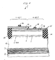
- the dopant in the donor layer 6 must not reach the first cap layer 8 or the buffer layer 4. More particularly, the spacer layer 5 must have sufficient width so that the 2-DEG remains in the buffer layer 4 after the annealing of the wafer 1. As shown in FIG.
- the layers 4, 5 and 6 are shown oriented horizontally with an energy diagram of the lower conduction band edge thereof in correspondence with the layer 4, 5 and 6.
- E F is the Fermi energy level of the shown structure.
- the width of the spacer layer 5 is critical in maintaining the 2-DEG in the proper position: in the potential well formed by the spacer layer 5 and the buffer layer 4. As discussed above, the width of the spacer layer 5 should be approximately 2.5 nanometers after annealing and have an aluminum concentration of approximately 22% for the proper confinement of the 2-DEG.
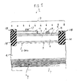
- a second isolation implant is done, referred to here as a deep isolation implant, assuring complete isolation of the E-HFETs and D-HFETs.
- a photoresist 20 (FIG. 6) is deposited and patterned, resulting in substantially the same pattern as the photoresist 12 of FIG. 2. This approach allows the use of similar masks for the patterning of photoresist 20 and photoresist 12.
- the wafer 1 is then exposed to an implant source (not shown) which provides an isolation dopant 21, preferably the same as that used for the shallow implant, e.g., oxygen.
- An exemplary implant is 2 ⁇ 1013 doubly ionized oxygen ions cm ⁇ 2 at 130 keV, resulting in a peak concentration of 5 ⁇ 1017 to 5 ⁇ 1018 atoms cm ⁇ 3.
- other implants could be used such as boron, argon or hydrogen.
- the isolation region 14 now extends at least through the superlattice structure 3, as shown in FIG. 8 after removal of the photoresist 20.
- This deep isolation implant removes virtually all possible low conductivity paths between HFETs separated by the isolation regions 14.
- the wafer 1 is then annealed in an atmosphere of helium or nitrogen at exemplary 500°C for 10 minutes or by rapid thermal anneal at an exemplary temperature of 550°C for 30 seconds.
- a photoresist 22 is deposited and patterned to expose the first and second cap layers 8, 10 where the contacts are to be formed.
- An exemplary first layer of a gold and germanium alloy is deposited either mixed together or in thin alternating sub-layers. Then an exemplary layer of nickel and lastly an exemplary layer of gold are deposited, all the layers collectively labeled here as 23, 23′. The first layer of gold:germanium alloy assures an ohmic contact to the doped GaAs first and second cap layers 8, 10.
- ohmic contacts can be used as the ohmic contacts to doped GaAs, such as gold:germanium/silver/gold or nickel/gold:germanium/gold.
- the unwanted metal 23′ is removed by "lifting off” the metal 23′ on the photoresist 22 as the photoresist 22 is removed.
- a barrier between the gold of the ohmic contacts and the aluminum is deposited as the top-most layer on the ohmic contact metal 23, such as Wi1Si 0.45 , WN or WSiN.
- the remaining ohmic contact metal 23 are the source and drain contacts of the E-HFETs and D-HFETs, as shown in FIG. 9.
- the wafer 1 is then annealed to alloy the metal ohmic contact 23 and form an ohmic contact with the underlying sources and drains.
- This ohmic anneal is a low temperature anneal of 350 - 450°C for 10 to 60 seconds in an atmosphere of helium or nitrogen.
- the deep isolation implant can occur after the deposition of the ohmic contacts metal 23, thereby combining the annealing steps for both the ohmic contact metals 23 and the deep isolation implant.
- a first insulating layer 24 typically silicon dioxide (SiO2) or silicon oxynitride (SiO x N y )
- SiO2 silicon dioxide
- SiO x N y silicon oxynitride
- a photoresist (not shown) is deposited and patterned to expose the first insulating layer 24 where windows, or vias, to underlying metal are desired, such as the drain and source contact metal 23 or the gates 17.
- the first insulating layer is then etched with a conventional anisotropic etch, such as a dry etch using SF6, NF3, or CF4.
- the photoresist (not shown) is then removed, the wafer 1 cleaned and a first metalization interconnect layer 25 is deposited.
- the first metalization interconnect layer 25 is preferably aluminum but gold (using a lift-off technique) could be used as metal 22.
- the thin barrier layer of W1Si 0.45 deposited on the ohmic contact metal 23 is used to prevent aluminum/gold interaction.
- a photoresist (not shown), is then deposited and patterned, leaving the metal interconnect layer 25 exposed where it is to be removed.
- the metal interconnect layer 25 is then etched and the photoresist (not shown) is removed, leaving the structure substantially as shown in FIG. 10.
- the first metal interconnect layer 25 is shown contacting the drain or source contacts of the exemplary E-HFETs and D-HFET in FIG. 10.
- the first insulating layer 24 may be optionally deposited very thickly, e.g. 800 nanometers, and etched back to form an essentially planar surface.
- the photoresist (not shown) is then deposited and patterned as described above.
- a second insulating layer 26 is deposited over the first metalization interconnect layer 25 and the first insulating layer 24 as shown in FIG. 11.
- the insulating layer 26 is similar to the composition of the first insulating layer 24.
- a photoresist layer (not shown) is deposited and patterned to expose windows in the second insulating layer 26 where windows, or vias, are to be formed for contacting underlying first metal interconnect layer 25.
- the second insulating layer 26 is then etched with a conventional anisotropic etch as described above.
- the photoresist (not shown) is then removed and a second metalization interconnect layer 27 is deposited.
- Another photoresist (not shown) is then deposited over the second metal interconnect layer 27 and patterned for removal of unwanted metal interconnect 27.
- the metal interconnect 27 is then etched and the photoresist (not shown) is removed.
- the second metal interconnect layer 27 is shown in FIG. 11 as contacting source and drain contacts of both exemplary E-HFET and D-HFET via the first level metal interconnect layer 25.
- the second level metal interconnect layer 27 (and any subsequent level of metal) is preferably of the same composition as the first level metal interconnect layer 25.
- interconnect metal 25, 27 are shown, other metal interconnect layers can be added to the structure shown in FIG. 11.
- layer 27 Over the last metal layer, here layer 27, another insulating layer 28 and then a passivation layer 29 is deposited to protect the completed circuit from contamination.
- the passivation layer 29 is preferably silicon nitride (Si3N4) or SiO x N y .
- the layers 28, 29 has deposited thereon a photoresist which is patterned to expose the layers 28, 29 where windows are to be formed for allowing bonding of external conductors (not shown) to the circuit.
- the layers 28, 29 are etched by a conventional anisotropic etch and photoresist (not shown) is removed, leaving windows therein to the underlying metal interconnect layer 27 for bonding pads and completing the wafer 1.
- the thicknesses of all the layers 4-10 and 24-29 are not to scale in all the figures.
- the combined layers 9 and 10 is approximately 50 nanometers, which is very small compared to the typical thickness of the first metal layer 25 (500 to 100 nanometers), making the entire structure of FIG. 9 substantially planar.
Abstract
Description
- A selectively doped heterostructure transistor, SDHT, (also known as a MODFET for modulation doped FET, a TEGFET for two-dimensional electron gas FET, or a HEMT for high electron mobility transistor, and will be referred to generically, for purposes here, as a heterojunction field effect transistor, or HFET) has supeprior performance compared to conventional (non-heterojunction) metal-semiconductor FETs (MESFET) in bandwidth and noise figure, etc. For example, see EP-A-0 005 059. One drawback to using HFETs is the difficulty in the formation thereof in integrated form with consistent device characteristics across a wafer, even across a single chip. For example, the threshold voltage of HFETs can vary so much in a single chip that logic circuits built using HFETs do not operate reliably, reducing the yield of operable circuits from a wafer.
- A new process has been invented for the manufacture of both enhancement and depletion HFETs in integrated form with consistent threshold voltages across a wafer and a self-aligned structure. In one embodiment, these advantages have been achieved generally by growing a buffer layer of compound semiconductor material with a first bandgap energy; growing a first spacer layer of compound semiconductor material with a second bandgap energy, growing a donor layer of doped compound semiconductor material with the second bandgap energy; growing a first cap layer of compound semiconductor material with the first bandgap energy; growing an etch-stop layer of compound semiconductor material with a third bandgap energy; and, growing a second cap layer of compound semiconductor material with the first bandgap energy. The second and third bandgap energies are more than the first bandgap energy. The layers are preferably grown by a molecular beam epitaxy process to achieve precise control over the thicknesses of the layers.
- A further embodiment, which generally achieves the above advantages and utilizes the epitaxial layer formed by the layers discussed above, involves isolating selected regions of the epitaxial layer; etching portions of the selected regions of the epitaxial layer to a predetermined depth where enhancement FETs are to be formed; forming gate electrodes for both enhancement and depletion FETs; forming source/drain regions for the drain and source electrodes of the enhancement and depletion FETs; contacting the source/drain regions, depositing a dielectric layer, selectively etching the dielectric for vias, forming an interconnect layer; and passivating the resulting structure. The steps of depositing a dielectric layer, selectively etching the dielectric layer for vias and forming an interconnect layer may be repeated for each desired layer of interconnect.
- The precise control over the thickness of the layers and the precision etching thereof ensures uniformity in the threshold voltages of the HFETs. The etch-stop layer allows for precision etching of the wafer where enhancement HFETs are to be formed. In addition, the resulting HFET structures are substantially planar, allowing for reliable metalization of the wafer.
- The method of isolating devices on the wafer is achieved generally by selectively implanting isolation dopant onto the wafer a predetermined depth into the epitaxial layer where conductivity therein is to be reduced; annealing the wafer at a predetermined temperature; selectively implanting isolation dopant into the wafer completely through the epitaxial layer into the substrate; and annealing the wafer a second time at a temperature less than the predetermined temperature.
- The foregoing features of this invention, as well as the invention itself, may be more fully understood from the following detailed description of the drawings representing one embodiment of the invention, in which:
- FIG. 1 is a cross-section view of a substrate with multiple layers grown thereon;
- FIG. 2 is the structure of FIG. 1 undergoing shallow isolation implant;
- FIG. 3 is the structure of FIG. 2 after a selective etch;
- FIG. 4 is the structure of FIG. 3 with gate metal deposited and patterned photoresist thereon;
- FIG. 5 is the structure of FIG. 4 with the gates for both enhancement and depletion HFETs in place and undergoing dopant implant;
- FIG. 6 is the structure of FIG. 5 after the implant of dopants to form the self-aligned HFET drain and source regions and undergoing a deep isolation implant;
- FIG. 7 is an energy diagram of the lower conduction band edge and the semiconductor layers corresponding thereto;
- FIG. 8 is the structure of FIG. 6 with patterned photoresist and metal deposited thereon for contacting the source/drain regions;
- FIG. 9 is the structure of FIG. 8 with photoresist and the unmasked metal removed leaving metal contacting the source/drain regions;
- FIG. 10 is the structure of FIG. 9 with a first dielectric layer and first metalization layer thereon; and,
- FIG. 11 is the completed structure of FIG. 10 with a second dielectric layer, second metalization layer and a passivation layer thereon.
- It is understood that none of the figures are to scale.
- Although the compound semiconductor material referred to here is based on gallium arsenide (GaAs) and aluminum gallium arsenide (AlGaAs), other compound semiconductor materials could be substituted, such as indium aluminum arsenide (InAlAs) and indium gallium arsenide (InGaAs), respectively. The concentration (i.e., mole fraction) of aluminum in the AlGaAs is usually identified as x in AlxGa1-xAs, where x can range from 0 (0%, or no aluminum) to 1 (100% aluminum, or no gallium), depending on the bandgap energy required of the material. Generally, the more the aluminum, the higher the bandgap energy of the AlGaAs material. For purposes here, gallium arsenide will be identified as GaAs and aluminum gallium arsenide will be identified as AlGaAs. The concentration of aluminum in AlGaAs will be designated by percentage of aluminum therein.
- Referring to FIG. 1, a partial cross-sectional view (not to scale) of a
wafer 1 ready for the manufacturing of both enhancement and depletion selectively doped heterojunction field-effect transistors (hereinafter referred to as E-HFET and D-HFET, respectively) is shown. Although not described in detail here,layers 3 through 11 (of whichlayers 4 through 10 are here referred to collectively as an epitaxial layer,layer 11 being a temporary layer) are grown on asemi-insulating GaAs substrate 2 in a molecular beam epitaxy (MBE) machine, forming an essentially continuous layer from thesubstrate 2. One such MBE machine capable of growing GaAs and AlGaAs layers is a Varian Gen II, manufactured by Varian Associates of Santa Clara, California. However, it is possible to grow GaAs and AlGaAs layers by metal-organic chemical vapor deposition (MOCVD) or by metal-organic or gas source MBE.Layer 3 contains therein multiple alternating layers of GaAs and AlGaAs to form a superlattice which reduces the likelihood that impurities and defects will propagate from thesubstrate 2 intohigher layers 4 through 10. This superlattice reduces the need for athicker buffer layer 4, decreasing the time necessary for the growth of the epitaxial layer. There is preferably more than ten of such alternating layers inlayer 3, each AlGaAs layer having an acceptable aluminum concentration of 10% to 60%. Each of the alternating layers has a thickness less than an electron or hole wave function, e.g., 4 nanometers or less. Using an exemplary aluminum concentration of 22%, it has been found that ten alternating layers, or periods, is sufficient. This results in the overall thickness of thelayer 3 of approximately 80 nanometers. - Over the superlattice (layer 3), a
buffer layer 4 of undoped GaAs is deposited having a typical thickness range of approximately 10 to 1000 nanometers, preferably 300 nanometers. As will be explained below, thebuffer layer 4 supports a two-dimensional electron gas (2-DEG), which is the channel, or active region, of the E-HFETs and D-HFETs. It is in the channel that current flows between the drain and source electrodes of corresponding E-HFETs and D-HFETs. - A
first spacer layer 5 is deposited over thebuffer layer 4, adonor layer 6 is deposited on thespacer layer 5, and asecond spacer layer 7 is deposited over the donor layer. The first and second spacer anddonor layers donor layer 6 is doped, and as will be explained in more detail below, the doping concentration strongly influences the threshold voltages of the D-HFETs and E-HFETs. To assure full depletion of thedonor layer 6 under zero bias conditions for an E-HFET, the donor layer should be less than 30 nanometers thick. Further, the acceptable uniform concentration of aluminum in thedonor layer 6 and thespacer layers wafer 1. The doping density in thedonor layer 6, prior to a subsequent wafer anneal step, ranges from 5x10¹⁷ to 2x10⁸ atoms cm⁻³ and is preferably 6x10¹⁷ atoms cm⁻³. Equivalently, beryllium, carbon or other suitable species could be used to make the conductivity of layer 6 P-type. As will be discussed in more detail below, thefirst spacer layer 5 enhances the electron mobility of the 2-DEG by confining the 2-DEG to thebuffer layer 4, thereby reducing scattering of the 2-DEG by impurities inlayers layers second spacer layer 7, along with thefirst spacer layer 5, functions to absorb out-diffusion of dopant from thedonor layer 6 during later high-temperature processing, such as annealing. The thickness of thespacer layer 5 is a trade-off between the transconductance of the desired E-HFET or D-HFET and the desired increase in mobility of the electrons in the 2-DEG, resulting in a thickness ranging from 1 to 5 nanometers, with approximately 2.5 nanometers as an acceptable compromise after a wafer annealing step, as discussed in more detail below. Likewise, the thickness of thesecond spacer layer 7 is similar to that for thefirst spacer layer 5. However, the primary purpose of thesecond layer 7 is to absorb dopant from thedonor layer 6 and prevent the dopant from reaching an upper layer and may have virtually no thickness after the anneal. In contrast, thefirst spacer layer 5 must be thick enough to properly confine the 2-DEG to thebuffer layer 4. Hence, the thickness of thesecond spacer layer 7 can be somewhat less than the thickness of thefirst spacer layer 5. - First and second cap layers 8, 10 are undoped GaAs layers used for forming thereon Schottky barrier gate contacts and ohmic drain and source contacts for E-HFETs and D-HFETs, respectively, as will be discussed in more detail below. The cap layers 8, 10 are approximately 10 nanometers thick. Undoped AlGaAs etch-
stop layer 9, disposed betweencap layers stop layer 9 ranges from 10% to 60% and is preferably 50%. - Last, a
protective layer 11 of AlGaAs is deposited, having a aluminum concentration substantially the same as the etch-stop layer 9 and a thickness of about that ofcap layers layer 11 is sacrificed to protect thewafer 1 from contamination or damage before a final etch and the deposition of metal to form the gates. - The doping of the
donor layer 6 and the distance the gates of the corresponding E-HFETs and D-HFETs are from the 2-DEG layer establishes the threshold voltages of the E-HFET and the D-HFETs. As will be discussed below, the corresponding distances are set by the thicknesses of the layers 5 - 10 for the D- HFETs and layers 5 - 8 for the E-HFETs. So critical are thickness of the layers 5 - 10 that for one tenth nanometer of error the threshold voltage of a D-HFET shifts approximately two to five millivolts and of an E-HFET shifts approximately two millivolts. Hence, once the desired characteristics of the E-HFETs and D-HFETs are determined and the doping density ofdonor layer 6 is set, the thicknesses of the layers 5 - 10 are calculated. Using the after-anneal doping densities given above fordonor layer 6, for an exemplary E-HFET having a threshold voltage of 0.2 volts, the combined thickness of layers 5 - 8 is substantially 50 nanometers. Similarly, for an exemplary D-HFET with a threshold voltage of - 0.6 volts, the combined thickness of layers 5 - 10 is substantially 100 nanometers. - As stated above, the epitaxial layer includes the
buffer layer 4, first and second spacer layers 5, 7,donor layer 6, first and second cap layers 8, 10 and the etch-stop layer 9. Thesuperlattice structure 3 and theprotective layer 11 are used advantageously in cooperation with the rest of the layers 4 - 10, but are not an indispensable portion of the claimed invention. Further, the first and second spacer layers 5,7 can be deleted fromwafer 1 when fabricating MESFET devices, mentioned above. - After formation of the
wafer 1, a shallow isolation of selected regions of the wafer is made. In FIG. 2, a layer of photoresist 12 (for example, Shipley AZ-1350J photoresist) is deposited and patterned, leaving exposed regions of thewafer 1 where an isolation well is to be formed. Typically, the entire wafer is exposed except where E-HFETs or D-HFETs are to be formed. An implant source (not shown) provides anisolation dopant 13, preferably ionized oxygen, which is driven into the wafer. Exemplary energy levels for the ionized oxygen range from 20 to 160 keV, with a dose of 5×10¹² to 1.5×10¹⁴ oxygen ions cm⁻²; the higher the energy, the deeper the implant. An exemplary implant is a dose of 1x10¹⁴ ions cm⁻² at 40 keV then at 125 keV. The resulting peak concentration of oxygen atoms in thewafer 1 ranges from 5×10¹⁸ to 1×10¹⁹ atoms cm⁻³. The implanted oxygen destroys the conductivity of the wafer where exposed to the implant, thereby isolating and reducing capacitive loading on devices later formed in thewafer 1. The resultingisolation regions 14 are formed, as shown in FIG. 3. - The
photoresist layer 12 of FIG. 2 is then removed and another photoresist is deposited (not shown). This photoresist is patterned to expose the underlying wafer in regions of the wafer where E-HFETs are to be formed. The exposedprotective layer 11 is then etched to thesecond cap layer 10 using an AlGaAs etchant described below. Thesecond cap layer 10 is itself etched to expose the etch-stop layer 9. The photoresist (not shown) is then removed and the wafer thoroughly cleaned. The previously un-etched portion ofprotective layer 11 and the exposed etch-stop layer 9 are then simultaneously etched to expose the portions of thesecond cap layer 10 where D-HFETs are to be formed and the portions of thefirst cap layer 8 where E-HFETs are to be formed. This results in the structure substantially as shown in FIG. 3. - The etching of the second cap layer 10 (GaAs) to the etch-
stop layer 9 is preferably by a wet etch of the wafer in a conventional potassium iodide/iodine (KI/I₂) solution until the GaAs is removed. Alternatively, a reactive ion etch could be used. Although the etch is selective, the over-etching of the GaAssecond cap layer 10 into the AlGaAs etch-stop layer 9 is not critical. Advantageously, the over-etching ofsecond cap layer 10 into the etch-stop layer 9 ensures complete removal of thesecond cap layer 10, resulting in a more uniform etch of etch-stop layer 9. It is noted, however, that the etching of the AlGaAsprotective layer 11 to thesecond cap layer 10 and the etching of the etch-stop layer 9 to thefirst cap layer 8 are critical to the performance of the later formed D-HFETs and E-HFETs as stated above. This etching must be both effective in removing all of the exposed AlGaAs as well as very selective to avoid over-etching and reducing the thickness of thefirst cap layer 8 and thesecond cap layer 10. details on the preferred etching process for selectively etching the AlGaAs layers 11 and 9 is given in the above-identified co-filed patent application by F. Ren et al. It is sufficient here to state that thewafer 1 is first cleaned with diluted (20:1 in water) ammonium hydroxide (NH₄OH), then etched with diluted (1:1 with water) hydrofluoric acid (HF) and again rinsed with diluted NH₄OH to achieve an etching selectivity of AlGaAs over GaAs of up to several hundred. - After the etching of the
protective layer 11 and the etch-stop layer 9, the structure shown in FIG. 3 results. The exposedfirst cap layer 8 will form the surface adjacent portions of the E-HFETs and thesecond cap layer 10 will form the surface adjacent portions of the D-HFETs. It is understood that the shallow isolation step discussed above can instead be done after the etching oflayers - Next, in FIG. 4, a uniformly thick layer of
refractory metal 15 is deposited onto the wafer to form the gates for the E-HFETs and D-HFETs. The preferred refectory metal for the gates is tungsten silicide (W₁Si0.45) and is sputtered on. However, tungsten nitride (WN) or tungsten silicide nitride (WSiN) can be used. The W₁Si0.45 has a high crystallization temperature (above 850°C) and remains amorphous following a subsequent high temperature anneal step, thus serving as a barrier to the inter-diffusion of Ga, As, W, and Si. Further, to reduce the resistivity of subsequently formed gates, a layer of tungsten could be deposited over the corresponding type of silicide. A layer of photoresist is then deposited over themetal 15 and patterned, leavingphotoresist 16 where the gates for the E-HFETs and D-HFETs are to be. The exposedmetal 15 is then etched, preferably by a reactive ion etch (RIE) using nitrogen trifluoride (NF₃), sulphur hexafluoride (SF₆) or carbon tetrafluoride (CF₄), leavingmetal 15 under the patternedphotoresist 16. - The patterned photoresist 16 (FIG. 4) is then removed, leaving
gates 17 in FIG. 5. Next, the source and drain regions of the E-HFETs and D-HFETs are to be formed by selectively implanting a dopant, here silicon, into the wafer to form N-type source and drain regions. First a layer ofphotoresist 18 is deposited and patterned to expose the portions of the wafer where it is desired to have the N-type regions formed. Shown here in FIG. 5, the patternedphotoresist 18 covers theisolation regions 14, but thephotoresist 18 may cover any area on the wafer. Next singly ionized silicon atoms 19, from an implant source (not shown), are implanted in the exposed wafer except where thephotoresist 18 andgates 17 covers thewafer 1. This process results in a self-aligned structure as shown in FIG. 6. After the implant, the photoresist layer 18 (FIG. 5) is removed. The effect of the implanting of silicon into thewafer 1 is the converting of the implanted layers to n-type, which is signified by "n" inlayers 4 though 10. The implanting of the silicon destroys the 2-DEG layer in the implanted regions of thebuffer layer 4, leaving the 2-DEG only in the unimplanted regions under thegates 17. Hence "transistor action" is possible only between the silicon implanted regions and is controlled by voltages applied togates 17. The concentration of implanted silicon in the epitaxial layers should be as high as possible to achieve as low as possible resistivity for the source and drain regions. The implant of silicon ions has an energy range of 20 to 150 keV and a dose of 3×10¹² to 3×10¹³ silicon ions cm⁻². An exemplary implant is a dose of 2×10¹³ ions cm⁻² at 30 keV and then a dose of 2×10¹³ ions cm⁻² at 120 keV. The resulting peak concentration of silicon ions in thewafer 1 before an annealing step ranges from 1×10¹⁸ to 3×10¹⁸ ions cm⁻³. Practically, the concentration of 2×10¹⁸ silicon ions cm⁻³ is the upper limit. Although it is preferable for source and drain regions (not shown) of the E-HFETs and D-HFETs to be the same conductivity type as the donor layer, here N-type, the source and drain regions can be P-type by implanting other dopants, such as beryllium, as discussed above. It is preferable that thedonor layer 6 be doped with the same dopant used for implanting. - High temperature annealing of the structure in FIG. 6 results in the activation of the silicon implant in the layers 4 - 10. An exemplary annealing step is the heating of the
wafer 1 to a temperature of approximately 800°C for approximately 10 minutes in an atmosphere of arsenic at pressure of 100 milliTorr or greater, preferably with a capping layer (not shown) of silicon dioxide (SiO₂), silicon oxynitride (SiOxNy) or silicon nitride (SixNy). Alternatively, a rapid thermal anneal could be used at an exemplary temperature of 825°C for 30 seconds. As stated, the silicon dopant in thedonor layer 6 out-diffuses and converts portions of the previously undoped AlGaAs spacer layers 5,7 into doped AlGaAs, which, for purpose here, becomes indistinguishable from thedonor layer 6, i.e., those portions of the spacer layers 5,7 that absorb dopant from thedonor layer 6 effectively becomes part ofdonor layer 6. However, as stated above, the dopant in thedonor layer 6 must not reach thefirst cap layer 8 or thebuffer layer 4. More particularly, thespacer layer 5 must have sufficient width so that the 2-DEG remains in thebuffer layer 4 after the annealing of thewafer 1. As shown in FIG. 7, thelayers layer spacer layer 5 is critical in maintaining the 2-DEG in the proper position: in the potential well formed by thespacer layer 5 and thebuffer layer 4. As discussed above, the width of thespacer layer 5 should be approximately 2.5 nanometers after annealing and have an aluminum concentration of approximately 22% for the proper confinement of the 2-DEG. - After the high temperature anneal of the
wafer 1, a second isolation implant is done, referred to here as a deep isolation implant, assuring complete isolation of the E-HFETs and D-HFETs. A photoresist 20 (FIG. 6) is deposited and patterned, resulting in substantially the same pattern as thephotoresist 12 of FIG. 2. This approach allows the use of similar masks for the patterning ofphotoresist 20 andphotoresist 12. Thewafer 1 is then exposed to an implant source (not shown) which provides anisolation dopant 21, preferably the same as that used for the shallow implant, e.g., oxygen. An exemplary implant is 2×10¹³ doubly ionized oxygen ions cm⁻² at 130 keV, resulting in a peak concentration of 5×10¹⁷ to 5×10¹⁸ atoms cm⁻³. However, it is understood that other implants could be used such as boron, argon or hydrogen. After the deep isolation implant, theisolation region 14 now extends at least through thesuperlattice structure 3, as shown in FIG. 8 after removal of thephotoresist 20. This deep isolation implant removes virtually all possible low conductivity paths between HFETs separated by theisolation regions 14. Thewafer 1 is then annealed in an atmosphere of helium or nitrogen at exemplary 500°C for 10 minutes or by rapid thermal anneal at an exemplary temperature of 550°C for 30 seconds. - Contacting the drain and source regions requires ohmic contacts to the surface adjacent portions of the doped first and second cap layers 8, 10. In FIG. 8, a
photoresist 22 is deposited and patterned to expose the first and second cap layers 8, 10 where the contacts are to be formed. An exemplary first layer of a gold and germanium alloy is deposited either mixed together or in thin alternating sub-layers. Then an exemplary layer of nickel and lastly an exemplary layer of gold are deposited, all the layers collectively labeled here as 23, 23′. The first layer of gold:germanium alloy assures an ohmic contact to the doped GaAs first and second cap layers 8, 10. Other metals and alloys can be used as the ohmic contacts to doped GaAs, such as gold:germanium/silver/gold or nickel/gold:germanium/gold. Theunwanted metal 23′ is removed by "lifting off" themetal 23′ on thephotoresist 22 as thephotoresist 22 is removed. As will be discussed in more detail below, if aluminum is used to interconnect devices onwafer 1, a barrier between the gold of the ohmic contacts and the aluminum is deposited as the top-most layer on theohmic contact metal 23, such as Wi₁Si0.45, WN or WSiN. - After removal of the
photoresist 22 andunwanted metal 23′ (FIG. 8), the remainingohmic contact metal 23 are the source and drain contacts of the E-HFETs and D-HFETs, as shown in FIG. 9. Thewafer 1 is then annealed to alloy the metalohmic contact 23 and form an ohmic contact with the underlying sources and drains. This ohmic anneal is a low temperature anneal of 350 - 450°C for 10 to 60 seconds in an atmosphere of helium or nitrogen. - It is noted that the deep isolation implant, discussed above, can occur after the deposition of the
ohmic contacts metal 23, thereby combining the annealing steps for both theohmic contact metals 23 and the deep isolation implant. After the ohmic anneal, a first insulatinglayer 24, typically silicon dioxide (SiO₂) or silicon oxynitride (SiOxNy), is deposited as shown in FIG. 10, preferably by plasma assisted chemical vapor deposition (PCVD). A photoresist (not shown) is deposited and patterned to expose the first insulatinglayer 24 where windows, or vias, to underlying metal are desired, such as the drain andsource contact metal 23 or thegates 17. The first insulating layer is then etched with a conventional anisotropic etch, such as a dry etch using SF₆, NF₃, or CF₄. The photoresist (not shown) is then removed, thewafer 1 cleaned and a firstmetalization interconnect layer 25 is deposited. The firstmetalization interconnect layer 25 is preferably aluminum but gold (using a lift-off technique) could be used asmetal 22. As discussed above, with aluminum metalization, the thin barrier layer of W₁Si0.45 deposited on theohmic contact metal 23 is used to prevent aluminum/gold interaction. A photoresist (not shown), is then deposited and patterned, leaving themetal interconnect layer 25 exposed where it is to be removed. Themetal interconnect layer 25 is then etched and the photoresist (not shown) is removed, leaving the structure substantially as shown in FIG. 10. The firstmetal interconnect layer 25 is shown contacting the drain or source contacts of the exemplary E-HFETs and D-HFET in FIG. 10. - To assist in planarizing the final structure, the first insulating
layer 24 may be optionally deposited very thickly, e.g. 800 nanometers, and etched back to form an essentially planar surface. The photoresist (not shown) is then deposited and patterned as described above. - A second insulating
layer 26 is deposited over the firstmetalization interconnect layer 25 and the first insulatinglayer 24 as shown in FIG. 11. The insulatinglayer 26 is similar to the composition of the first insulatinglayer 24. A photoresist layer (not shown) is deposited and patterned to expose windows in the second insulatinglayer 26 where windows, or vias, are to be formed for contacting underlying firstmetal interconnect layer 25. The second insulatinglayer 26 is then etched with a conventional anisotropic etch as described above. The photoresist (not shown) is then removed and a secondmetalization interconnect layer 27 is deposited. Another photoresist (not shown) is then deposited over the secondmetal interconnect layer 27 and patterned for removal ofunwanted metal interconnect 27. Themetal interconnect 27 is then etched and the photoresist (not shown) is removed. The secondmetal interconnect layer 27 is shown in FIG. 11 as contacting source and drain contacts of both exemplary E-HFET and D-HFET via the first levelmetal interconnect layer 25. The second level metal interconnect layer 27 (and any subsequent level of metal) is preferably of the same composition as the first levelmetal interconnect layer 25. - Although only two layers of
interconnect metal layer 27, another insulatinglayer 28 and then apassivation layer 29 is deposited to protect the completed circuit from contamination. Thepassivation layer 29 is preferably silicon nitride (Si₃N₄) or SiOxNy. The layers 28, 29 has deposited thereon a photoresist which is patterned to expose thelayers layers metal interconnect layer 27 for bonding pads and completing thewafer 1. - It is noted that the thicknesses of all the layers 4-10 and 24-29 are not to scale in all the figures. In particular the combined
layers
Claims (20)
growing a buffer layer (4) of compound semiconductor material with a first bandgap energy;
growing a donor layer (6) of doped compound semiconductor material with a second bandgap energy;
growing a first cap layer (8) of compound semiconductor material with the first bandgap energy;
growing an etch-stop layer (9) of compound semiconductor material with a third bandgap energy; and
growing a second cap layer (10) of compound semiconductor with the first bandgap energy;
wherein the second and third bandgap energies are greater than the first bandgap energy;
growing a first spacer layer (5) of compound semiconductor material with the second bandgap energy; and,
growing a second spacer layer (7) of compound semiconductor material with the second bandgap energy;
wherein the first spacer layer is disposed between the buffer layer and the donor layer and the second spacer layer is disposed between the donor layer and the first cap layer.
growing a protective layer (11) of compound semiconductor material with the third bandgap energy;
wherein the protective layer is grown on the second cap layer.
selectively etching the protective layer where an E-HFET is to be formed;
etching the exposed second cap layer to expose the etch-stop layer;
etching the exposed etch-stop layer and the remaining protective layer to expose the major surface of the first cap layer and the second cap layer, respectively;
depositing gate metal (15); and
selectively etching the gate metal to form gates for E-HFETs and D-HFETs on the major surfaces of the first and second cap layers, respectively.
a buffer layer (4) of compound semiconductor material with a first bandgap energy;
a donor layer (6) of doped compound semiconductor material with a second bandgap energy and disposed over the first spacer layer;
a first cap layer (8) of compound semiconductor material with the first bandgap energy and disposed over the donor layer;
an etch-stop layer (9) of compound semiconductor material with a third bandgap energy and disposed over the first cap layer; and,
a second cap layer (10) of compound semiconductor material with the first bandgap energy and disposed over the etch-stop layer;
wherein the second and third bandgap energies are greater than the first bandgap energy and the first cap layer forms the major surface for later-formed E-HFETs and the second cap layer forms the major surface for later-formed D-HFETs
a first spacer layer (5) of compound semiconductor material with the second bandgap energy and disposed between the donor layer and the buffer layer; and
a second spacer layer (7) of compound semiconductor material with the second bandgap energy and disposed between the donor layer and the first cap layer.
a protective layer (11) of compound semiconductor material with the third bandgap energy and disposed over the second cap layer.
forming a buffer sub-layer (4) of undoped compound semiconductor with a first bandgap energy;
forming a spacer sub-layer (5) of undoped compound semiconductor with a second bandgap energy;
forming a donor sub-layer (6) of doped compound semiconductor with the second bandgap energy;
forming a first cap sub-layer (8) of undoped compound semiconductor with first bandgap energy;
forming an etch-stop sub-layer (9) of undoped compound semiconductor with a third bandgap energy; and,
forming a second cap sub-layer (10) of undoped compound semiconductor with the first bandgap energy;
wherein the second and third bandgap energies are greater than the first bandgap energy.
depositing refractory metal (15);
depositing photoresist (16);
patterning the photoresist; and,
etching the photoresist and the refractory metal.
depositing photoresist (17, 18);
patterning the photoresist as to leave exposed the areas of the epitaxial layer where the drain and source electrodes of the enhancement and depletion FETs are to be formed;
implanting dopant species (19) into the exposed areas; and,
annealing the epitaxial layer.
depositing photoresist (22);
patterning the photoresist as to leave windows on the source/drain regions where an ohmic contact is to occur;
depositing metal (23);
etching the metal to leave metal remaining in the windows; and,
annealing the remaining metal.
depositing photoresist (20);
patterning the photoresist to remove portions thereof over the selected regions of the epitaxial layer;
implanting an isolation dopant (21) in the exposed epitaxial layer, and,
annealing the epitaxial layer.
depositing photoresist over the corresponding dielectric layer (24, 26);
patterning the photoresist; and,
etching the exposed dielectric layer.
depositing a passivation layer (29);
depositing photoresist;
patterning the photoresist as to leave windows over bonding pads; and,
etching the passivation layer in the windows.
selectively implanting isolation dopant (21) into the wafer a predetermined depth into the epitaxial layer where conductivity therein is to be reduced;
annealing the wafer at a predetermined temperature;
selectively implanting isolation dopant into the wafer completely through the epitaxial layer into the substrate; and
annealing the wafer a second time at a temperature less than the predetermined temperature.
depositing a photoresist (20) over the epitaxial layer;
patterning the photoresist to remove portions thereof over the selected portions of the epitaxial layer, and
implanting the isolation dopant (21) into the exposed epitaxial layers.
Applications Claiming Priority (2)
| Application Number | Priority Date | Filing Date | Title |
|---|---|---|---|
| US290932 | 1988-12-28 | ||
| US07/290,932 US5041393A (en) | 1988-12-28 | 1988-12-28 | Fabrication of GaAs integrated circuits |
Publications (2)
| Publication Number | Publication Date |
|---|---|
| EP0378894A2 true EP0378894A2 (en) | 1990-07-25 |
| EP0378894A3 EP0378894A3 (en) | 1990-11-28 |
Family
ID=23118113
Family Applications (1)
| Application Number | Title | Priority Date | Filing Date |
|---|---|---|---|
| EP19890308623 Withdrawn EP0378894A3 (en) | 1988-12-28 | 1989-08-24 | Fabrication of gaas integrated circuits |
Country Status (3)
| Country | Link |
|---|---|
| US (1) | US5041393A (en) |
| EP (1) | EP0378894A3 (en) |
| JP (1) | JP2930982B2 (en) |
Cited By (3)
| Publication number | Priority date | Publication date | Assignee | Title |
|---|---|---|---|---|
| FR2656466A1 (en) * | 1989-12-25 | 1991-06-28 | Mitsubishi Electric Corp | COMPOUND SEMICONDUCTOR INTEGRATED CIRCUIT HAVING AN IMPLANTED REGION. |
| EP0469768A1 (en) * | 1990-07-31 | 1992-02-05 | AT&T Corp. | A substantially linear field effect transistor and method of making same |
| FR2707042A1 (en) * | 1993-06-25 | 1994-12-30 | Mitsubishi Electric Corp |
Families Citing this family (32)
| Publication number | Priority date | Publication date | Assignee | Title |
|---|---|---|---|---|
| US5192701A (en) * | 1988-03-17 | 1993-03-09 | Kabushiki Kaisha Toshiba | Method of manufacturing field effect transistors having different threshold voltages |
| JPH0444328A (en) * | 1990-06-11 | 1992-02-14 | Mitsubishi Electric Corp | Semiconductor device and manufacture thereof |
| US5173761A (en) * | 1991-01-28 | 1992-12-22 | Kobe Steel Usa Inc., Electronic Materials Center | Semiconducting polycrystalline diamond electronic devices employing an insulating diamond layer |
| CA2067025A1 (en) * | 1991-04-26 | 1992-10-27 | Nobuo Shiga | Multi-stage amplifier device and method for producing the same |
| JPH0521468A (en) * | 1991-07-17 | 1993-01-29 | Sumitomo Electric Ind Ltd | Manufacture of field-effect transistor |
| KR940006711B1 (en) * | 1991-09-12 | 1994-07-25 | 포항종합제철 주식회사 | Manufacturing method of delta doping quantum fet |
| DE4219523A1 (en) * | 1992-06-15 | 1993-12-16 | Daimler Benz Ag | Monolithically integrated millimeter wave circuit and method for its production |
| US5254492A (en) * | 1992-11-10 | 1993-10-19 | Texas Instruments Incorporated | Method of fabricating an integrated circuit for providing low-noise and high-power microwave operation |
| US5374328A (en) * | 1993-03-25 | 1994-12-20 | Watkins Johnson Company | Method of fabricating group III-V compound |
| US5349214A (en) * | 1993-09-13 | 1994-09-20 | Motorola, Inc. | Complementary heterojunction device |
| JPH0786310A (en) * | 1993-09-20 | 1995-03-31 | Mitsubishi Electric Corp | Method for forming metal gate electrode having high melting point |
| US5514606A (en) * | 1994-07-05 | 1996-05-07 | Motorola | Method of fabricating high breakdown voltage FETs |
| US5539248A (en) | 1995-11-13 | 1996-07-23 | Motorola | Semiconductor device with improved insulating/passivating layer of indium gallium fluoride (InGaF) |
| US5672522A (en) * | 1996-03-05 | 1997-09-30 | Trw Inc. | Method for making selective subcollector heterojunction bipolar transistors |
| US5698870A (en) * | 1996-07-22 | 1997-12-16 | The United States Of America As Represented By The Secretary Of The Air Force | High electron mobility transistor (HEMT) and pseudomorphic high electron mobility transistor (PHEMT) devices with single layer integrated metal |
| US5698900A (en) * | 1996-07-22 | 1997-12-16 | The United States Of America As Represented By The Secretary Of The Air Force | Field effect transistor device with single layer integrated metal and retained semiconductor masking |
| US5939764A (en) * | 1997-04-23 | 1999-08-17 | President And Fellows Of Harvard College | Direct current voltage transformer |
| US6242293B1 (en) | 1998-06-30 | 2001-06-05 | The Whitaker Corporation | Process for fabricating double recess pseudomorphic high electron mobility transistor structures |
| US6060402A (en) * | 1998-07-23 | 2000-05-09 | The Whitaker Corporation | Process for selective recess etching of epitaxial field effect transistors with a novel etch-stop layer |
| US6307221B1 (en) | 1998-11-18 | 2001-10-23 | The Whitaker Corporation | InxGa1-xP etch stop layer for double recess pseudomorphic high electron mobility transistor structures |
| KR100385856B1 (en) * | 2000-12-27 | 2003-06-02 | 한국전자통신연구원 | Fabrication method of self-aligned gate transistor |
| US6703638B2 (en) * | 2001-05-21 | 2004-03-09 | Tyco Electronics Corporation | Enhancement and depletion-mode phemt device having two ingap etch-stop layers |
| WO2003015174A2 (en) * | 2001-08-07 | 2003-02-20 | Jan Kuzmik | High electron mobility devices |
| US20060014334A1 (en) * | 2001-10-12 | 2006-01-19 | J R P Augusto Carlos | Method of fabricating heterojunction devices integrated with CMOS |
| US6893947B2 (en) * | 2002-06-25 | 2005-05-17 | Freescale Semiconductor, Inc. | Advanced RF enhancement-mode FETs with improved gate properties |
| JP3858888B2 (en) * | 2003-12-02 | 2006-12-20 | ソニー株式会社 | Etching method and semiconductor device manufacturing method |
| KR100615598B1 (en) * | 2004-07-19 | 2006-08-25 | 삼성전자주식회사 | Semiconductor Devices Having A Planarization Isolating Layer And Methods Of Forming The Same |
| JP5112620B2 (en) * | 2005-05-31 | 2013-01-09 | オンセミコンダクター・トレーディング・リミテッド | Compound semiconductor device |
| US20080258242A1 (en) * | 2007-04-19 | 2008-10-23 | Northrop Grumman Space And Mission Systems Corp. | Low contact resistance ohmic contact for a high electron mobility transistor and fabrication method thereof |
| US8470652B1 (en) | 2011-05-11 | 2013-06-25 | Hrl Laboratories, Llc | Monolithic integration of group III nitride enhancement layers |
| US8927999B2 (en) | 2011-11-21 | 2015-01-06 | Avogy, Inc. | Edge termination by ion implantation in GaN |
| RU2570099C1 (en) * | 2014-08-05 | 2015-12-10 | Акционерное общество "Научно-производственное предприятие "Исток" имени А.И. Шокина" (АО "НПП "Исток" им. Шокина") | Manufacturing method of semiconductor heterostructure |
Citations (2)
| Publication number | Priority date | Publication date | Assignee | Title |
|---|---|---|---|---|
| EP0119089A2 (en) * | 1983-03-14 | 1984-09-19 | Fujitsu Limited | GaAs semiconductor device and a method of manufacturing it |
| EP0175437A1 (en) * | 1984-05-01 | 1986-03-26 | Fujitsu Limited | Production of GaAs enhancement and depletion mode HEMT's |
Family Cites Families (20)
| Publication number | Priority date | Publication date | Assignee | Title |
|---|---|---|---|---|
| JPS5856270B2 (en) * | 1977-01-11 | 1983-12-14 | 財団法人半導体研究振興会 | Insulated gate electrostatic induction field effect transistor |
| US4163237A (en) * | 1978-04-24 | 1979-07-31 | Bell Telephone Laboratories, Incorporated | High mobility multilayered heterojunction devices employing modulated doping |
| US4194935A (en) * | 1978-04-24 | 1980-03-25 | Bell Telephone Laboratories, Incorporated | Method of making high mobility multilayered heterojunction devices employing modulated doping |
| JPS5676547A (en) * | 1979-11-27 | 1981-06-24 | Fujitsu Ltd | Semiconductor device |
| JPS57192083A (en) * | 1981-05-22 | 1982-11-26 | Hitachi Ltd | Semiconductor device |
| JPS58130559A (en) * | 1981-11-02 | 1983-08-04 | テキサス・インスツルメンツ・インコ−ポレイテツド | Iii-v group bipolar integrated circuit device |
| JPS5918679A (en) * | 1982-07-22 | 1984-01-31 | Fujitsu Ltd | Semiconductor device |
| JPS59191386A (en) * | 1983-04-14 | 1984-10-30 | Nec Corp | Semiconductor device and manufacture thereof |
| JPS60116178A (en) * | 1983-11-29 | 1985-06-22 | Fujitsu Ltd | Semiconductor device and manufacture thereof |
| EP0143656B1 (en) * | 1983-11-29 | 1989-02-22 | Fujitsu Limited | Compound semiconductor device and method of producing it |
| JPS6113630A (en) * | 1984-06-28 | 1986-01-21 | Fujitsu Ltd | Manufacture of semiconductor device |
| JPS6135567A (en) * | 1984-07-27 | 1986-02-20 | Sony Corp | Semiconductor device |
| JPS61107758A (en) * | 1984-10-31 | 1986-05-26 | Fujitsu Ltd | Gaas integrated circuit and manufacture thereof |
| JPS62111474A (en) * | 1985-11-11 | 1987-05-22 | Hitachi Ltd | Semiconductor integrated circuit device |
| DE3751243T2 (en) * | 1986-02-18 | 1995-08-31 | Toshiba Kawasaki Kk | Optoelectronic component and method for its production. |
| US4771013A (en) * | 1986-08-01 | 1988-09-13 | Texas Instruments Incorporated | Process of making a double heterojunction 3-D I2 L bipolar transistor with a Si/Ge superlattice |
| JPH0666420B2 (en) * | 1987-01-27 | 1994-08-24 | 富士通株式会社 | Semiconductor integrated circuit device and manufacturing method thereof |
| KR880010509A (en) * | 1987-02-11 | 1988-10-10 | 오레그 이. 앨버 | Field effect transistor |
| US4860064A (en) * | 1987-10-21 | 1989-08-22 | American Telephone And Telegraph Company At&T Bell Laboratories | Transistor comprising a 2-dimensional carrier gas collector situated between emitter and gate |
| JP2503594B2 (en) * | 1988-06-28 | 1996-06-05 | 日本電気株式会社 | Semiconductor integrated device and manufacturing method thereof |
-
1988
- 1988-12-28 US US07/290,932 patent/US5041393A/en not_active Expired - Lifetime
-
1989
- 1989-08-24 EP EP19890308623 patent/EP0378894A3/en not_active Withdrawn
- 1989-08-28 JP JP1218764A patent/JP2930982B2/en not_active Expired - Lifetime
Patent Citations (2)
| Publication number | Priority date | Publication date | Assignee | Title |
|---|---|---|---|---|
| EP0119089A2 (en) * | 1983-03-14 | 1984-09-19 | Fujitsu Limited | GaAs semiconductor device and a method of manufacturing it |
| EP0175437A1 (en) * | 1984-05-01 | 1986-03-26 | Fujitsu Limited | Production of GaAs enhancement and depletion mode HEMT's |
Non-Patent Citations (4)
| Title |
|---|
| IEEE ELECTRON DEVICE LETTERS, vol. EDL-8, no. 3, March 1987, pages 121-123, New York, US; H. SHICHIJO et al.: "GaAs E/D MESFET 1-kbit static RAM fabricated on silicon substrate". * |
| IEEE TRANSACTIONS ON MICROWAVE THEORY AND TECHNIQUES, vol. MIT-34, no. 12, December 1986, pages 1522-1527, IEEE, New York, US; K. TANAKA et al.: "Low-noise HEMT using MOCVD". * |
| JOURNAL OF ELECTROCHEMICAL SOCIETY, vol. 135, no. 11, November 1988, pages 2835-2840; K.T. SHORT et al.: "Implant isolation of GaAs". * |
| NUCLEAR INSTRUMENTS & METHODS IN PHYSICS RESEARCH, vols. 209/210, part II, May 1983, pages 657-661, North-Holland Publishing Co., Amsterdam, NL; X.-C. DENG: "Oxygen ion beam modification of GaAs". * |
Cited By (4)
| Publication number | Priority date | Publication date | Assignee | Title |
|---|---|---|---|---|
| FR2656466A1 (en) * | 1989-12-25 | 1991-06-28 | Mitsubishi Electric Corp | COMPOUND SEMICONDUCTOR INTEGRATED CIRCUIT HAVING AN IMPLANTED REGION. |
| US5166768A (en) * | 1989-12-25 | 1992-11-24 | Mitsubishi Denki Kabushiki Kaisha | Compound semiconductor integrated circuit device with an element isolating region |
| EP0469768A1 (en) * | 1990-07-31 | 1992-02-05 | AT&T Corp. | A substantially linear field effect transistor and method of making same |
| FR2707042A1 (en) * | 1993-06-25 | 1994-12-30 | Mitsubishi Electric Corp |
Also Published As
| Publication number | Publication date |
|---|---|
| US5041393A (en) | 1991-08-20 |
| JP2930982B2 (en) | 1999-08-09 |
| JPH02205362A (en) | 1990-08-15 |
| EP0378894A3 (en) | 1990-11-28 |
Similar Documents
| Publication | Publication Date | Title |
|---|---|---|
| US5041393A (en) | Fabrication of GaAs integrated circuits | |
| US5606184A (en) | Heterostructure field effect device having refractory ohmic contact directly on channel layer and method for making | |
| US5480829A (en) | Method of making a III-V complementary heterostructure device with compatible non-gold ohmic contacts | |
| US4636822A (en) | GaAs short channel lightly doped drain MESFET structure and fabrication | |
| EP0119089B1 (en) | Gaas semiconductor device and a method of manufacturing it | |
| US4711858A (en) | Method of fabricating a self-aligned metal-semiconductor FET having an insulator spacer | |
| US6893947B2 (en) | Advanced RF enhancement-mode FETs with improved gate properties | |
| US5036017A (en) | Method of making asymmetrical field effect transistor | |
| US4855246A (en) | Fabrication of a gaas short channel lightly doped drain mesfet | |
| EP0631324A1 (en) | Method of making ohmic contacts to a complementary semiconductor device | |
| JPH11354541A (en) | Semiconductor device and its manufacture | |
| EP0201873B1 (en) | A method of the production of a metal semiconductor field effect transistor and said transistor | |
| JP3233207B2 (en) | Method for manufacturing field effect transistor | |
| US6455361B1 (en) | Semiconductor device and manufacturing method of the same | |
| EP0367411A2 (en) | Heterojunction semiconductor devices and methods of making the same | |
| US5411903A (en) | Self-aligned complementary HFETS | |
| US4895811A (en) | Method of manufacturing semiconductor device | |
| JPH0846182A (en) | Manufacture semiconductor device | |
| JP3035917B2 (en) | Field effect type semiconductor device and method of manufacturing the same | |
| JPH0249012B2 (en) | HANDOTAISOCHINOSEIZOHOHO | |
| JP4186267B2 (en) | Method for manufacturing compound semiconductor device | |
| EP0684633A2 (en) | Method for manufacturing a semiconductor device | |
| JP3834074B2 (en) | Method for forming ohmic contacts in complementary semiconductor devices | |
| JP3710613B2 (en) | Semiconductor device | |
| JPH0429225B2 (en) |
Legal Events
| Date | Code | Title | Description |
|---|---|---|---|
| PUAI | Public reference made under article 153(3) epc to a published international application that has entered the european phase |
Free format text: ORIGINAL CODE: 0009012 |
|
| AK | Designated contracting states |
Kind code of ref document: A2 Designated state(s): DE FR GB |
|
| PUAL | Search report despatched |
Free format text: ORIGINAL CODE: 0009013 |
|
| AK | Designated contracting states |
Kind code of ref document: A3 Designated state(s): DE FR GB |
|
| 17P | Request for examination filed |
Effective date: 19901212 |
|
| 17Q | First examination report despatched |
Effective date: 19921019 |
|
| STAA | Information on the status of an ep patent application or granted ep patent |
Free format text: STATUS: THE APPLICATION IS DEEMED TO BE WITHDRAWN |
|
| 18D | Application deemed to be withdrawn |
Effective date: 19930430 |