EP0389242B1 - Data base processing system using multiprocessor system - Google Patents
Data base processing system using multiprocessor system Download PDFInfo
- Publication number
- EP0389242B1 EP0389242B1 EP90302972A EP90302972A EP0389242B1 EP 0389242 B1 EP0389242 B1 EP 0389242B1 EP 90302972 A EP90302972 A EP 90302972A EP 90302972 A EP90302972 A EP 90302972A EP 0389242 B1 EP0389242 B1 EP 0389242B1
- Authority
- EP
- European Patent Office
- Prior art keywords
- local
- processing operation
- resource
- shared
- data base
- Prior art date
- Legal status (The legal status is an assumption and is not a legal conclusion. Google has not performed a legal analysis and makes no representation as to the accuracy of the status listed.)
- Expired - Lifetime
Links
- 238000012545 processing Methods 0.000 title claims description 170
- 230000015654 memory Effects 0.000 claims description 103
- 238000001514 detection method Methods 0.000 claims description 69
- 238000006243 chemical reaction Methods 0.000 description 21
- 238000010586 diagram Methods 0.000 description 12
- 238000000034 method Methods 0.000 description 11
- 239000003795 chemical substances by application Substances 0.000 description 10
- 238000004891 communication Methods 0.000 description 9
- 230000006870 function Effects 0.000 description 5
- 230000003111 delayed effect Effects 0.000 description 3
- 230000008878 coupling Effects 0.000 description 2
- 238000010168 coupling process Methods 0.000 description 2
- 238000005859 coupling reaction Methods 0.000 description 2
- 230000006872 improvement Effects 0.000 description 2
- 230000004044 response Effects 0.000 description 2
- 230000002776 aggregation Effects 0.000 description 1
- 238000004220 aggregation Methods 0.000 description 1
- 238000007796 conventional method Methods 0.000 description 1
- 239000008187 granular material Substances 0.000 description 1
- 230000004048 modification Effects 0.000 description 1
- 238000012986 modification Methods 0.000 description 1
- 230000003287 optical effect Effects 0.000 description 1
- 230000009467 reduction Effects 0.000 description 1
Images


Classifications
-
- G—PHYSICS
- G06—COMPUTING; CALCULATING OR COUNTING
- G06F—ELECTRIC DIGITAL DATA PROCESSING
- G06F9/00—Arrangements for program control, e.g. control units
- G06F9/06—Arrangements for program control, e.g. control units using stored programs, i.e. using an internal store of processing equipment to receive or retain programs
- G06F9/46—Multiprogramming arrangements
- G06F9/52—Program synchronisation; Mutual exclusion, e.g. by means of semaphores
- G06F9/524—Deadlock detection or avoidance
-
- G—PHYSICS
- G06—COMPUTING; CALCULATING OR COUNTING
- G06F—ELECTRIC DIGITAL DATA PROCESSING
- G06F13/00—Interconnection of, or transfer of information or other signals between, memories, input/output devices or central processing units
- G06F13/14—Handling requests for interconnection or transfer
- G06F13/36—Handling requests for interconnection or transfer for access to common bus or bus system
-
- Y—GENERAL TAGGING OF NEW TECHNOLOGICAL DEVELOPMENTS; GENERAL TAGGING OF CROSS-SECTIONAL TECHNOLOGIES SPANNING OVER SEVERAL SECTIONS OF THE IPC; TECHNICAL SUBJECTS COVERED BY FORMER USPC CROSS-REFERENCE ART COLLECTIONS [XRACs] AND DIGESTS
- Y10—TECHNICAL SUBJECTS COVERED BY FORMER USPC
- Y10S—TECHNICAL SUBJECTS COVERED BY FORMER USPC CROSS-REFERENCE ART COLLECTIONS [XRACs] AND DIGESTS
- Y10S707/00—Data processing: database and file management or data structures
- Y10S707/912—Applications of a database
- Y10S707/922—Communications
-
- Y—GENERAL TAGGING OF NEW TECHNOLOGICAL DEVELOPMENTS; GENERAL TAGGING OF CROSS-SECTIONAL TECHNOLOGIES SPANNING OVER SEVERAL SECTIONS OF THE IPC; TECHNICAL SUBJECTS COVERED BY FORMER USPC CROSS-REFERENCE ART COLLECTIONS [XRACs] AND DIGESTS
- Y10—TECHNICAL SUBJECTS COVERED BY FORMER USPC
- Y10S—TECHNICAL SUBJECTS COVERED BY FORMER USPC CROSS-REFERENCE ART COLLECTIONS [XRACs] AND DIGESTS
- Y10S707/00—Data processing: database and file management or data structures
- Y10S707/99931—Database or file accessing
- Y10S707/99938—Concurrency, e.g. lock management in shared database
Definitions
- the present invention relates to a data base processing system using a multiprocessor system, more particularly, it relates to a data base processing system enabling dynamic switching between a local processing operation and a shared processing operation in accordance with an access state to a resource.
- the resource is a unit of the data base to be processed.
- the local processing operation is an operation for locally processing the data mainly by using control data on a local memory
- the shared processing operation is an operation for processing the data mainly by using control data on a shared memory.
- the present invention also relates to a deadlock detection system enabling improvement of throughout an entire data base processing system using the multiprocessor
- Multiprocessor systems can be roughly divided into a fine coupling type and a coarse coupling type.
- multiprocessor systems for example, a complex type combining the above two types, and an intermediate type between the above two types.
- a data base processing system utilizes a multiprocessor system because a limitation of response (limitation of throughput of the system) occurs in a one processor system.
- a limitation of response limitation of throughput of the system
- the data base is also managed to raise the throughput of the system, by using the multiprocessor system, it is necessary to ensure an "integrity guarantee" for maintaining the data base in a normal state.
- the necessary time for the integrity guarantee tends to considerably increase in the multiprocessor system because the integrity guarantee must be ensured in every processor. Accordingly, it is necessary to efficiently perform the integrity guarantee to increase throughput of the multiprocessor system. Further, it is necessary to efficiently perform the deadlock detection in the data base processing system.
- EP-A-0 286 807 discloses a data base processing system according to the preamble of accompanying claim 1.
- a shared processing operation is not performed symmetrically, but rather involves one of the processor modules obtaining a lock on (sole interest in) a resource held in the shared memory before it can have access thereto.
- a central processor maintains a concordance of resource identities.
- a data base processing system using a multi-processor system constituted by: a plurality of processor modules, each having a local memory and connected to each other through a high speed bus line, and a shared memory connected to said plurality of processor modules through said high speed bus line; said data base processing system containing resources located both in the shared memory and in the local memories and further comprising:
- An embodiment of the present invention desirably further comprises a deadlock detection system including: a transaction management information area provided in the shared memory for managing transactions between the processor modules; a first directed graph information area provided in the shared memory for indicating a waiting state between transactions operated on by different processor modules; a deadlock detection unit provided in each of the processor modules for detecting a deadlock; and a second directed graph information area provided in the local memory for indicating a waiting state between transactions each operating within the processor modules; wherein deadlock detection is separately performed between local deadlock detection and global deadlock detection in such a way that the waiting state of the transaction is searched in accordance with the first and second directed graph information on the shared memory and local memory.
- a deadlock detection system including: a transaction management information area provided in the shared memory for managing transactions between the processor modules; a first directed graph information area provided in the shared memory for indicating a waiting state between transactions operated on by different processor modules; a deadlock detection unit provided in each of the processor modules for detecting a deadlock; and a second directed graph information area
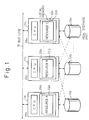
- Figures 1 and 2 show an example of a previously-considered data processing system using a multiprocessor system
- reference numbers 11a to 11n denote processor modules, each having a central processing unit (CPU) and local memory 25. Each processor module 11 is connected through a bus line 12 so that it is possible to carry out communication between processor modules.
- Reference numbers 22a to 22n denote data base to be controlled. Each resource 22a to 22n is provided in each processor module 11a to 11n.
- reference numbers 13a to 13n denote real storage units each provided as secondary data memory.
- an access to the resource 22 is managed by so-called "granules", i.e., a unit of a given data set (a data set is an aggregation of data) existing in the data base.
- This unit may be indicated by, for example, a file level or a record level.
- the integrity of the data can be achieved, for example, by preventing an occurrence of contradiction of data caused by competition of access, or by recovering from a fault.
- reference number 10 denotes a shared memory having a plurality of resources 22.
- the resources 22 read out from the real storage unit 13 are provided in the shared memory 10 which can be accessed from each processor module 11.
- the exclusive control and buffer control are processed in common in the whole system. That is, each processor module 11 symmetrically and commonly performs processing of exclusive control and buffer control in the whole system so that the high integrity guarantee can be realized in shared processing operation of the whole system.
- the integrity guarantee is performed based on only two methods as explained above. That is, one integrity guarantee is only performed in the local processing operation in every processor module 11 as shown in Fig. 1, and the other integrity guarantee is only performed in the shared processing in the whole system as shown in Fig. 2.
- the processor module 11a accesses the resource B (22b)
- the processor module 11a generates a request to lock operation for exclusive control and a request for buffer access to the processor module 11b by utilizing the communication between processor modules through the bus 12.
- overhead a rate of real time taken to run a management program out of the overall operation time of a computer
- throughput is considerably reduced in the special resource 22 which can be accessed by a plurality of processor modules.
- it is difficult to perform a tuning operation adjustment of a system to effectively assign resources in accordance with an amount of work and features of the work) because an operator must assign an optimal resource with reference to access data statistically obtained.
- Figure 3 is a schematic block diagram of a data base processing system according to an embodiment of the present invention.
- reference number 20 denotes a storage unit provided in the shared memory 10 for storing information for management of the data base, such as the access state of the data base and shared/local processing operations.
- 21 denotes a storage unit also provided in the shared memory 10 for storing lock information for exclusive control.
- 23 denotes an access management unit provided in the processor module 11 to manage the access state of the resource.
- 24 denotes a conversion control unit for controlling the switching between the local processing operation and the shared processing operation.
- 26 denotes a storage unit provided in a local memory 25 of the processor module 11 for storing local lock information for exclusive control.
- Each processor module (11-1, 11-2, ...) having the local memory 25 is connected to the shared memory 10 through the high speed bus line 12. Further, in this system, each real storage unit 13 is connected to each processor module through an I/O bus line 14 so that it is possible for each processor module 11 to equally access the real storage unit 13.
- the management of the resource of the data base is performed based on the management information set in the data base management information storage unit 20.
- the storage unit 20 is provided in the shared memory 10 in this embodiment, it is possible to provide it in the local memory 25.
- shared/local display area 20-1 indicates that the resource 22, which becomes the object of the access, is either the object of the shared processing operation or the object of the local processing operation. Further, an area 20-2 is also provided in the storage unit 20 for storing the access state of the resource.
- Each processor module has the same structure, and comprises the access management unit 23 and the shared/local conversion control unit 24.
- the access management unit 23 has a management function of both the resource 22 in the shared memory 10 and the resource in the local memory 25.
- each processor module 11 symmetrically performs the processing of the integrity guarantee for the resource 22.
- the word "symmetrically” means that the control is performed by the same processing sequence even if no processor module accesses the resource 22.
- the decision, whether the access control to the resource 22 is performed by either the shared processing operation or by the local processing operation, is performed with reference to the shared/local display unit 20-1 of the storage unit 20.
- the shared/local conversion control unit 24 manages the access state (20-2) for every resource 22.
- the conversion control unit 24 determines such resource is the object of the local processing operation for the special processor module.
- the conversion control unit 24 determines such resource is the object of the shared processing operation. Accordingly, the conversion control unit 24 always supervises the access state of each resource 22 and performs the conversion control from the shared processing operation to the local processing operation and vice versa by updating the shared/local display unit 20-1.
- Figure 4 is a diagram for use in explaining an operation of an embodiment of the present invention.
- the feature of the present invention lies in, in the management of the resource of the data base, dynamic switching between the local processing operation and the shared processing operation in accordance with the access state of the resource based on the shared/local conversion control.
- the local processing operation is mainly performed in the local memory and the shared processing operation is mainly performed in the shared memory.
- the exclusive control and buffer control of the resource are performed by the special processor module managing that resource.
- the access to the resource is unevenly distributed to the special processor module, it is possible to achieve high speed access control by locally performing the exclusive control and buffer control.
- the processing operation may be delayed compared with the local processing operation since the integrity guarantee is performed in the whole system.
- the access operation is not unevenly distributed to the special processor module, it is possible to avoid a concentration of load on the special processor module when the resource is uniformly accessed by all processor modules.
- the local processing operation is performed.
- the shared processing operation is performed.
- the above switching is dynamically performed by the shared/local conversion control unit. As a result, it is possible to perform optimal access management in accordance with the access state of the resource.
- FIG. 5 is a schematic block diagram of a multiprocessor system applying an embodiment of the present invention.
- SSU denotes a shared memory unit
- SCA denotes an I/O interface adapter
- DK denotes a disk unit
- DLP denotes a data link processor
- DRC denotes a driver/receiver card.
- 12 denotes a high speed bus
- 14 denotes an I/O bus.
- each processor module (PM) 11 has at least one CPU and local memory 25.
- the processor module 11 can access the shared memory unit SSU through the high speed bus 12 under control of a bus controller (not shown).
- Each processor module 11 is constituted so as to be able to perform the processing operation of other processor modules in turns. Accordingly, when a fault occurs in one processor module, that processor module is disconnected from the system and the processing operation is continued by another processor module in turn.
- the content of the data base is stored in the disk unit DK, for example, an optical disk device or a magnetic disk.
- the disk unit DK can be accessed by any processor module through the I/O bus 14 and the I/O interface adapter SCA.
- FIGS. 6 and 7 are views for explaining a processing operation of an access request from a terminal unit.
- Fig. 6 is a flowchart of the processing operation from an input of a message until start of an application program.
- APP denotes the application program.
- Fig. 7 is a flowchart of the processing operation at the data base management unit. Reference numbers 1 ⁇ to 9 ⁇ in these drawings correspond to the following item numbers.
- a message for example, a data base search request, is input from the terminal unit to the processor module 11.
- the processor module 11 performs a given processing operation in response to the message.
- the terminal unit may previously determine the special processor module carrying the special message.
- the application program APP to which the message is distributed, starts to execute.
- the application program APP can perform the access request to the data base management unit based on a data base operation language if necessary.
- the access management unit 23 performs the exclusive control for the resource receiving the access request, i.e., the lock control to avoid the competition for access, in accordance with the interface of the application program.
- This exclusive control is selectively performed in accordance with whether the resource to be accessed becomes the object of the shared processing operation or the object of the local processing operation. Accordingly, the effective lock management is selectively performed either in the whole system or only the special processor module.
- the shared memory and the local memory are, for example, selectively utilized in accordance with whether the resource to be accessed becomes the object of the shared processing operation or the object of the local processing operation.
- the buffer control is performed after the above selection between the object of the shared processing operation and the object of the local processing operation.
- the result of the access is informed to the application program APP receiving the access request.
- the shared/local conversion control unit 24 manages and maintains the access state at each processor module.
- the shared/local conversion control unit 24 also performs the collection of the information to judge either the object of the shared processing operation or the object of the local processing operation for each resource.
- the shared/local conversion control unit 24 investigates the frequency of the access for each resource. That is, the unit 24 investigates whether or not the frequency of the access is concentrated on a particular processor module. The unit 24 determines whether the management of the shared processing operation or the management of the local processing operation should be done.
- the conversion processing operation is performed in the shared/local conversion control unit 24 to convert from the shared processing operation to the local processing operation, or vice versa. This conversion is performed in such a way that the management information and the resource are moved between the shared memory and the local memory.
- the shared/local conversion control unit 24 periodically performs the above conversion in accordance with a predetermined interval or at a suitable timing.
- Figure 8 is a view for explaining management data to be used in the shared and local processing operations according to the present invention.
- reference number 30 denotes a space management table for storing space management information for management of the data base.
- Reference number 31 denotes a data base attribute table for storing various information regarding the resource.
- Reference number 33 denotes a data base access state table for storing the access state of every processor module.
- the processor module can comprise a plurality of address spaces, and the management of the data base and the address space is performed by a kernel (main program for operation system (OS) to manage resource, service, etc.) provided in common to each address space. Further, the processor module has a back-up function used when a space fault accidentally occurs.
- the space management table further comprises a pointer function for pointing to the data base attribute table 31.
- the data base attribute table 31 has the following information for every resource.
- the data base access table 33 has the following information used to manage the access state at every resource. This information includes the number of access times from each processor module.
- the space management table 30, the data base attribute table 31, and the data base access state table 33 are provided in the shared memory and local memory, respectively.
- the data base attribute table 31 and the data base access state table 33 are provided in the local memory of the processor module performing the local processing control.
- the data base attribute table 31 is provided in the shared memory.
- the data base access table 33 is provided in both the shared memory and the local memory.
- the processor module updates only access state information for its own processor module.
- the access state data from each processor module is collected in the shared memory at predetermined time intervals.
- Figure 9 is a flowchart for explaining shared/local conversion control in an embodiment of the present invention.
- the judgement is performed as to whether the resource is fixed to the shared processing type or the local processing type. Regardless of the access state, when the operator or the system manager fixedly designates one of the above types for the resource, the conversion control between the shared processing and the local processing is not performed.
- the judgement is performed based on the data base attribute table as to whether the current resource belongs to the shared processing operation or the local processing operation.
- the step 4 ⁇ is selected (YES).
- the step 9 ⁇ is selected (NO).
- the judgement is performed as to whether or not the processing should be moved to the local processing operation.
- the access state is investigated as to whether the number of access times at one processor module is considerably larger than that of the other processor module with reference to the result of the access state.
- NO the processing of the resource is completed.
- the local processor module PM is determined in such a way that the processor module, which ensures the integrity of the resource determined as the local processing type, is recognized as the processor module to which access is considerably large.
- the data base access state table is cleared in this step.
- the management information is moved to the processor module performing the integrity guarantee hereinafter. That is, data base access state table is used for the local processing operation.
- the buffer control is moved to the local processing management.
- the management of the newest data base is performed by the processor module determined as the local processing type.
- the data base buffer of the resource is moved to the buffer provided in the local memory of the processor module performing the local processing operation to improve the access efficiency of the data base.
- the processor module performing the local processing operation registers the access state in accordance with the access request from each processor module.
- the number of access times of the processor module performing the local processing operation is smaller than that of the access to the other processor module, that resource is determined as the shared processing type and steps to are performed as explained below. In this case, when the locality is incorrect, the operation is moved to other local PM. This step is also added to the step 4 ⁇ .
- the data base access state table is cleared in this step.
- the management information is moved from the local memory of the processor module performing the integrity guarantee hereinafter to the shared memory. That is, the buffer control is moved to the shared processing management.
- the management of the newest data is also performed by the shared processing management. That is, the resource is symmetrically managed by each processor module.
- the data base buffer for the resource is moved to the shared memory so that it is possible to improve the efficiency for the reference from the other processor module.
- either the integrity guarantee for the processing operation or the integrity guarantee for the local processing operation can be automatically selected in accordance with the access state for the resource of the data base. Accordingly, it is possible to achieve high speed access control between the processor modules. Further, it is possible to achieve reduction of the overhead in the communication between the processor modules so that it is possible to raise the throughput of the whole system.
- Another aspect of the present invention relates to a deadlock detection system in the data base processing system using the multiprocessor system shown in Figs. 3 and 4.
- Figures 10 to 12 are views for explaining a deadlock state in the exclusive control under the lock control
- Figure 13 is a view for explaining one example of a WFG.
- the order of the reference and the order of update to the special resource between the request sources needing the same resource is defined by designating the mode of the lock (a shared mode or an exclusive mode) for the resource and the name of the resource. As a result of determination of the processing order, the integrity of the resource can be easily ensured.
- T1 and T2 denote transactions, and R1 and R2 denote resources.
- the transaction is a unit of sequential data or a request for processing of data input from a terminal.
- This drawing shows the state in which first, the transaction T1 performs the lock control of the resource R1 under the shared mode S, and second, the transaction T2 requests the lock control under the exclusive mode X. In this case, the lock control request from the transaction T2 is delayed until the transaction T1 releases the lock control.
- a deadlock occurring in this exclusive control is a problem to be solved.
- the deadlock state occurs when two request sources are simultaneously requesting lock control of the special resource and both are waiting for the order of the lock control between two request sources.
- the transaction T1 performs the lock control of the resource R1 in the shared mode and waits for the release of the lock of the resource R2 in the exclusive mode.
- the transaction T2 simultaneously performs the lock control of the resource R2 in the shared mode and waits for the release of the lock of the resource R1 in the exclusive mode.
- the transaction T1 waits for the transaction T2, and the transaction T2 waits for the transaction T1. Accordingly, the deadlock state occurs between the two transactions T1 and T2 because neither processing operation at T1 and T2 can be completed.
- a directed graph is used in deadlock detection.
- the directed graph represents the waiting state between transactions under the lock control.
- the deadlock detection is performed by detecting a closed loop in the directed graph.
- the directed graph is called a WFG (wait For Graph).
- FIG. 13 is a view for explaining one example of a WFG.
- T1 to T7 denote transactions.
- Each arrow line between transactions denotes a waiting state.
- the lines T1 ⁇ T2 ⁇ T6 ⁇ T7 ⁇ T5 ⁇ T1 constitute one closed loop. That is, T1 waits for T2, T2 waits for T6, T6 waits for T7, T7 waits for T5, and T5 waits for T1. Accordingly, the deadlock state occurs in this closed loop.
- the deadlock state can be released by cutting the loop in such a way that any one of the requests is processed as an error in the transaction.
- the special processor module carries a heavy load since such a special processor module mainly controls the deadlock detection. Second, the cost for maintaining the whole WFG is large. Third, when a fault occurs in the special processor module, the influence of the fault affects the whole system.
- a deadlock detection system according to an embodiment of the present invention is explained in detail below.
- FIG 14 is a schematic block diagram of a deadlock detection system according to an embodiment of the present invention.
- This drawing corresponds to Fig. 3. Accordingly, the shared memory 10 and the processor module 11 are the same as shown in Fig. 3, but the deadlock detection function is added to the shared memory 10 and the processor module 11 as shown in Figs. 23 and 24.
- the shared memory 10 includes the transaction management information area 130 for managing the transaction, and the global WFG information area 140 for indicating the waiting state of the transaction between the processor modules.
- the processor module 11 comprises a deadlock detection unit 150, and the local memory 25 includes the local WFG information area 160.
- the deadlock is detected by utilizing the directed graph indicating the wait state between the transactions.
- the local WFG i.e., the directed graph information indicating the wait state between the transactions operating within the same processor modules
- An agent information of other system which indicates that the transaction of other system waits for own transaction, is set in the shared memory as the directed graph information indicating the wait state between the transactions operating across different processor modules.
- the local WFG provided in the local memory and global WFG are provided in the shared memory, it is possible to separate a local deadlock detection and a global deadlock detection.
- the deadlock detection unit 150 detects the waiting state in accordance with the directed graph information in the shared memory 10 and the local memory 25. When a closed loop is detected, the deadlock detection unit 150 recognizes the occurrence of the deadlock and starts to perform the processing for releasing the deadlock.
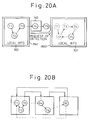
- Figure 15A is a view for explaining the relationship between the local WFG and the global WFG.
- a transaction indicating a waiting state between other transactions within the same processor module is managed in each processor module based on the following:
- the T5 (dotted circle) waits for the T1 and the T5 has only identification of the T1 (dotted circle). Further, the T1 waits for the T2, and the T4 waits for the T3.
- the structure of the WFG has the agent information on the shared memory in the case of the shared/local processing.
- Fig. 15B is in the case of the waiting state of the T3 and T4 for the lock operation to the resource of the shared processing.
- the agent is provided on the shared memory when the lock is requested from the other processor module.
- it is necessary to perform the message communication when preparing the WFG. In this case, the message communication is not affected to the performance of the transaction since the WFG is asynchronously provided.
- the deadlock detection is performed for the T1 on the shared memory after the local deadlock detection is performed on the T2.
- the waiting state which the T1 waits for the T2 can judge since the agent of the T2 exists on the shared memory and it can discriminate on the shared memory.
- the local WFG only used within the processor module is provided in the local memory 25, and the global WFG used between the processor modules is provided in the shared memory 10. Accordingly, it is possible to solve a drawback of the conventional art as explained below.
- each processor module completely and independently performs deadlock detection with reference to the information in the shared memory 10.
- each processor module cooperatively performs deadlock detection with reference to shared information in the shared memory 10.
- the deadlock detection may be omitted taking into consideration the load on the system, and transactions over a predetermined defined time may be stopped.
- Figure 16 is a view for explaining resource management information.
- the (a) portion denotes management information of the resources R1, R2, R3 which become the object of the lock control
- (b) and (c) portions denote the management information of the waiting state.
- each of the (b) transactions maintains the lock state of the corresponding resource.
- each of the (c) transactions maintains the waiting state for the release of the transaction.
- the transaction T1 maintains the lock of the resource R1, and the transaction T2 waits for the release of the lock of the resource R1 from the transaction R1.
- the transaction T4 also waits for the transaction T2.
- Figure 17 is a directed graph indicating the waiting state of the resource management information shown in Fig. 16. As explained in Fig. 12, for example, the right direction arrow indicates that T2 waits for T1.
- the WFG information is expressed by a table and a link information (identification information).
- Figures 18 to 20B are views for explaining the configuration of deadlock detection according to the present invention.
- the deadlock detection is performed in steps of; first, investigating the loop of the graph based on the local WFG information, second, accessing the shared memory 10 when the waiting state for the agent exists and finally referring to the global WFG information.
- the processor module PM1 sends a subgraph of its own local WFG information to the processor module PM2 through the message communication, and requests the detection of the deadlock to the processor module PM2. Accordingly, the processor module PM2 can detect the occurrence of the deadlock based on the subgraph and its own local WFG information.
- FIG 21 is a WFG control table provided for every transaction having a waiting state.
- the WFG control table 30 comprises the following area (a) to (e).
- the information for selecting the transaction subject to release of the deadlock is set in this area.
- This area is temporarily used during the detection of the deadlock.
- the identifier of the transaction having the waiting state is stored in this area.
- the identifier of the processor module which is operating on the transaction, or the identifier of the subsystem managing the data base being operated on by the processor module is set in this area.
- the pointer designating the transaction having a waiting state, to the WFG control table is stored in this area.
- a plurality of waiting states a plurality of areas are prepared in this table.
- Figure 22 is a view for explaining the WFG control table shown in Fig. 21.
- reference number 31 denotes an index table.
- Each of the WFG control tables 30 is pointed at from the index table 31, and they are linked with each other as shown in the drawing.
- an index table for starting the deadlock detection is provided in the local memory 25 and the start point of the deadlock detection is detection is determined with reference to the index table.
- the algorithm of the deadlock detection i.e., the processing operation of the deadlock detection unit 150 shown in Fig. 14, is explained in detail hereinafter.
- the cycle from the transaction of the subgraph of the requested WFG to the same transaction is found, and the above fact is judged as a deadlock.
- the transaction subject to the release of the deadlock is selected from the transaction at this judged system, or from the transaction constituting the subgraph.
- the transaction having the least amount of damage when stopping the processing operation is selected based on the control information of the transaction.
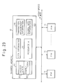
- Figure 23 is a schematic block diagram of a shared memory including a data base processing system and a deadlock detection system
- Fig. 24 is a schematic block diagram of a processor module including a data base processing system and a deadlock detection system.
- the internal structure of the shared memory 10 used for the data base processing system is shown in Fig. 3, and the internal structure of the shared memory 10 used for the deadlock detection system is shown in Fig. 14.
- the shared memory comprises the transaction management information and the global WFG information
- the processor module comprises the deadlock detection function and the local WFG information in the local memory.
Description
Claims (2)
- A data base processing system using a multi-processor system constituted by: a plurality of processor modules (11), each having a local memory (25) and connected to each other through a high speed bus line (12), and a shared memory (10) connected to said plurality of processor modules (11) through said high speed bus line (12); said data base processing system containing resources located both in the shared memory and in the local memories and further comprising:characterised in that:a storage means (20) for storing data base management information representing, for every resource of the data base, whether it is an object of a shared processing operation or an object of a local processing operation (20-1), as well as the access state of the resource (20-2) ;an access management means (23) provided in each of said processor modules for performing an access control for an access request to said data base under either said shared processing operation or said local processing operation in accordance with said data base management information (20-1), said local processing operation being asymmetrically performed in only the one processor module (11) which is assigned to the resource being the object of the access request; anda control means (24) provided in each of said processor modules for managing the access state (20-2) of each resource, and for controlling the shifting between the local processing operation and the shared processing operation;said storage means (20) is provided in said shared memory (10);said shared processing operation is symmetrically performed by each of the processor modules (11);and in that said shifting between the local processing operation and the shared processing operation is controlled by said control means (24) in such a way that: when the frequency of the access to a resource is unevenly distributed to a particular processor module (11), the resource is determined as the object of said local processing operation at said particular processor module; and when said frequency of the access is not unevenly distributed to a particular processor module, the resource is determined as the object of said shared processing operation.
- A data base processing system as claimed in claim 1, further comprising a deadlock detection system, said deadlock detection system comprising:a transaction management information area (130) provided in said shared memory (10) for managing transactions between said processor modules (11);a first directed graph information area (140) provided in said shared memory (10) for indicating a waiting state between transactions each being operated on by different processor modules;a deadlock detection means (150) provided in each of said processor modules (11) for detecting a deadlock; anda second directed graph information area (160) provided in said local memory (25) for indicating a waiting state between transactions each operating within said processor modules;wherein deadlock detection is separately performed between local deadlock detection and global deadlock detection in such a way that the waiting state of the transaction is searched in accordance with said first and second directed graph information in said shared memory and local memory.
Applications Claiming Priority (4)
| Application Number | Priority Date | Filing Date | Title |
|---|---|---|---|
| JP1068815A JPH07120305B2 (en) | 1989-03-20 | 1989-03-20 | Database processing method by multiprocessor |
| JP68815/89 | 1989-03-20 | ||
| JP1068814A JP2825839B2 (en) | 1989-03-20 | 1989-03-20 | Deadlock detection processing method |
| JP68814/89 | 1989-03-20 |
Publications (3)
| Publication Number | Publication Date |
|---|---|
| EP0389242A2 EP0389242A2 (en) | 1990-09-26 |
| EP0389242A3 EP0389242A3 (en) | 1993-06-30 |
| EP0389242B1 true EP0389242B1 (en) | 1998-05-27 |
Family
ID=26410003
Family Applications (1)
| Application Number | Title | Priority Date | Filing Date |
|---|---|---|---|
| EP90302972A Expired - Lifetime EP0389242B1 (en) | 1989-03-20 | 1990-03-20 | Data base processing system using multiprocessor system |
Country Status (7)
| Country | Link |
|---|---|
| US (1) | US5649184A (en) |
| EP (1) | EP0389242B1 (en) |
| KR (1) | KR930000853B1 (en) |
| AU (1) | AU614225B2 (en) |
| CA (1) | CA2011807C (en) |
| DE (1) | DE69032337T2 (en) |
| ES (1) | ES2116267T3 (en) |
Families Citing this family (42)
| Publication number | Priority date | Publication date | Assignee | Title |
|---|---|---|---|---|
| JPH0962586A (en) * | 1995-08-25 | 1997-03-07 | Fujitsu Ltd | Information processor and data processing method for this processor |
| JP3857409B2 (en) * | 1998-03-17 | 2006-12-13 | 富士通株式会社 | Distributed processing system, distributed processing method, and computer-readable recording medium recording distributed processing program |
| JP2000047994A (en) * | 1998-07-27 | 2000-02-18 | Fujitsu Ltd | Information processor |
| US7346910B1 (en) * | 2000-05-26 | 2008-03-18 | International Business Machines Incorporation | Administration of groups of computer programs, data processing systems, or system resources |
| EP1170665B1 (en) * | 2000-07-06 | 2004-02-04 | Texas Instruments France | Multi-processor system verification circuitry |
| US7233998B2 (en) * | 2001-03-22 | 2007-06-19 | Sony Computer Entertainment Inc. | Computer architecture and software cells for broadband networks |
| US7549145B2 (en) * | 2003-09-25 | 2009-06-16 | International Business Machines Corporation | Processor dedicated code handling in a multi-processor environment |
| US7496917B2 (en) * | 2003-09-25 | 2009-02-24 | International Business Machines Corporation | Virtual devices using a pluarlity of processors |
| US7478390B2 (en) * | 2003-09-25 | 2009-01-13 | International Business Machines Corporation | Task queue management of virtual devices using a plurality of processors |
| US7516456B2 (en) * | 2003-09-25 | 2009-04-07 | International Business Machines Corporation | Asymmetric heterogeneous multi-threaded operating system |
| US7475257B2 (en) * | 2003-09-25 | 2009-01-06 | International Business Machines Corporation | System and method for selecting and using a signal processor in a multiprocessor system to operate as a security for encryption/decryption of data |
| US7389508B2 (en) * | 2003-09-25 | 2008-06-17 | International Business Machines Corporation | System and method for grouping processors and assigning shared memory space to a group in heterogeneous computer environment |
| US20050071828A1 (en) * | 2003-09-25 | 2005-03-31 | International Business Machines Corporation | System and method for compiling source code for multi-processor environments |
| US7415703B2 (en) * | 2003-09-25 | 2008-08-19 | International Business Machines Corporation | Loading software on a plurality of processors |
| US7523157B2 (en) * | 2003-09-25 | 2009-04-21 | International Business Machines Corporation | Managing a plurality of processors as devices |
| US7444632B2 (en) * | 2003-09-25 | 2008-10-28 | International Business Machines Corporation | Balancing computational load across a plurality of processors |
| US20050289143A1 (en) * | 2004-06-23 | 2005-12-29 | Exanet Ltd. | Method for managing lock resources in a distributed storage system |
| US7735089B2 (en) * | 2005-03-08 | 2010-06-08 | Oracle International Corporation | Method and system for deadlock detection in a distributed environment |
| US7616218B1 (en) * | 2005-12-05 | 2009-11-10 | Nvidia Corporation | Apparatus, system, and method for clipping graphics primitives |
| JP2007328461A (en) * | 2006-06-06 | 2007-12-20 | Matsushita Electric Ind Co Ltd | Asymmetric multiprocessor |
| US8347064B1 (en) | 2006-09-19 | 2013-01-01 | Nvidia Corporation | Memory access techniques in an aperture mapped memory space |
| US8352709B1 (en) | 2006-09-19 | 2013-01-08 | Nvidia Corporation | Direct memory access techniques that include caching segmentation data |
| US8543792B1 (en) | 2006-09-19 | 2013-09-24 | Nvidia Corporation | Memory access techniques including coalesing page table entries |
| US8601223B1 (en) | 2006-09-19 | 2013-12-03 | Nvidia Corporation | Techniques for servicing fetch requests utilizing coalesing page table entries |
| US8707011B1 (en) | 2006-10-24 | 2014-04-22 | Nvidia Corporation | Memory access techniques utilizing a set-associative translation lookaside buffer |
| US8700883B1 (en) | 2006-10-24 | 2014-04-15 | Nvidia Corporation | Memory access techniques providing for override of a page table |
| US8706975B1 (en) | 2006-11-01 | 2014-04-22 | Nvidia Corporation | Memory access management block bind system and method |
| US8607008B1 (en) | 2006-11-01 | 2013-12-10 | Nvidia Corporation | System and method for independent invalidation on a per engine basis |
| US8533425B1 (en) | 2006-11-01 | 2013-09-10 | Nvidia Corporation | Age based miss replay system and method |
| US8504794B1 (en) | 2006-11-01 | 2013-08-06 | Nvidia Corporation | Override system and method for memory access management |
| US8347065B1 (en) * | 2006-11-01 | 2013-01-01 | Glasco David B | System and method for concurrently managing memory access requests |
| US8700865B1 (en) | 2006-11-02 | 2014-04-15 | Nvidia Corporation | Compressed data access system and method |
| US8543773B2 (en) | 2008-08-25 | 2013-09-24 | International Business Machines Corporation | Distributed shared memory |
| US9411661B2 (en) * | 2009-04-08 | 2016-08-09 | International Business Machines Corporation | Deadlock avoidance |
| US10146545B2 (en) | 2012-03-13 | 2018-12-04 | Nvidia Corporation | Translation address cache for a microprocessor |
| US9880846B2 (en) | 2012-04-11 | 2018-01-30 | Nvidia Corporation | Improving hit rate of code translation redirection table with replacement strategy based on usage history table of evicted entries |
| US10241810B2 (en) | 2012-05-18 | 2019-03-26 | Nvidia Corporation | Instruction-optimizing processor with branch-count table in hardware |
| US9104502B2 (en) | 2012-12-15 | 2015-08-11 | International Business Machines Corporation | Managing resource pools for deadlock avoidance |
| US20140189310A1 (en) | 2012-12-27 | 2014-07-03 | Nvidia Corporation | Fault detection in instruction translations |
| US10108424B2 (en) | 2013-03-14 | 2018-10-23 | Nvidia Corporation | Profiling code portions to generate translations |
| TWI513230B (en) * | 2013-04-29 | 2015-12-11 | Ind Tech Res Inst | Remote management systems and apparatuses for cwmp and methods for improving the cwmp performance thereof |
| CN108809863A (en) * | 2017-05-05 | 2018-11-13 | 中国航空无线电电子研究所 | A kind of on-board data storage resource Distributed sharing network system based on AFDX |
Family Cites Families (18)
| Publication number | Priority date | Publication date | Assignee | Title |
|---|---|---|---|---|
| GB1504112A (en) * | 1976-03-17 | 1978-03-15 | Ibm | Interactive enquiry systems |
| US4320451A (en) * | 1974-04-19 | 1982-03-16 | Honeywell Information Systems Inc. | Extended semaphore architecture |
| US4189771A (en) * | 1977-10-11 | 1980-02-19 | International Business Machines Corporation | Method and means for the detection of deadlock among waiting tasks in a multiprocessing, multiprogramming CPU environment |
| US4245306A (en) * | 1978-12-21 | 1981-01-13 | Burroughs Corporation | Selection of addressed processor in a multi-processor network |
| US4707781A (en) * | 1979-01-09 | 1987-11-17 | Chopp Computer Corp. | Shared memory computer method and apparatus |
| US4484262A (en) * | 1979-01-09 | 1984-11-20 | Sullivan Herbert W | Shared memory computer method and apparatus |
| US4574350A (en) * | 1982-05-19 | 1986-03-04 | At&T Bell Laboratories | Shared resource locking apparatus |
| US4494193A (en) * | 1982-09-30 | 1985-01-15 | At&T Bell Laboratories | Deadlock detection and resolution scheme |
| US4648035A (en) * | 1982-12-06 | 1987-03-03 | Digital Equipment Corporation | Address conversion unit for multiprocessor system |
| US4591977A (en) * | 1983-03-23 | 1986-05-27 | The United States Of America As Represented By The Secretary Of The Air Force | Plurality of processors where access to the common memory requires only a single clock interval |
| JPS6054052A (en) * | 1983-09-02 | 1985-03-28 | Nec Corp | Processing continuing system |
| JPS6171750A (en) * | 1984-09-17 | 1986-04-12 | Kokusai Denshin Denwa Co Ltd <Kdd> | Protocol verification system |
| US5123101A (en) * | 1986-11-12 | 1992-06-16 | Xerox Corporation | Multiple address space mapping technique for shared memory wherein a processor operates a fault handling routine upon a translator miss |
| US4843542A (en) * | 1986-11-12 | 1989-06-27 | Xerox Corporation | Virtual memory cache for use in multi-processing systems |
| US5142683A (en) * | 1987-03-09 | 1992-08-25 | Unisys Corporation | Intercomputer communication control apparatus and method |
| JPS63263557A (en) * | 1987-04-13 | 1988-10-31 | インターナシヨナル・ビジネス・マシーンズ・コーポレーシヨン | Adjustment of access by simultaneous transaction for hierarchical related resource |
| US5251308A (en) * | 1987-12-22 | 1993-10-05 | Kendall Square Research Corporation | Shared memory multiprocessor with data hiding and post-store |
| US5058006A (en) * | 1988-06-27 | 1991-10-15 | Digital Equipment Corporation | Method and apparatus for filtering invalidate requests |
-
1990
- 1990-03-15 CA CA002011807A patent/CA2011807C/en not_active Expired - Fee Related
- 1990-03-19 AU AU52001/90A patent/AU614225B2/en not_active Ceased
- 1990-03-20 ES ES90302972T patent/ES2116267T3/en not_active Expired - Lifetime
- 1990-03-20 EP EP90302972A patent/EP0389242B1/en not_active Expired - Lifetime
- 1990-03-20 US US07/495,982 patent/US5649184A/en not_active Expired - Fee Related
- 1990-03-20 DE DE69032337T patent/DE69032337T2/en not_active Expired - Fee Related
- 1990-03-20 KR KR1019900003741A patent/KR930000853B1/en not_active IP Right Cessation
Also Published As
| Publication number | Publication date |
|---|---|
| AU614225B2 (en) | 1991-08-22 |
| CA2011807A1 (en) | 1990-09-20 |
| EP0389242A3 (en) | 1993-06-30 |
| CA2011807C (en) | 1999-02-23 |
| KR900015010A (en) | 1990-10-25 |
| EP0389242A2 (en) | 1990-09-26 |
| KR930000853B1 (en) | 1993-02-06 |
| US5649184A (en) | 1997-07-15 |
| AU5200190A (en) | 1990-09-27 |
| DE69032337D1 (en) | 1998-07-02 |
| ES2116267T3 (en) | 1998-07-16 |
| DE69032337T2 (en) | 1998-09-24 |
Similar Documents
| Publication | Publication Date | Title |
|---|---|---|
| EP0389242B1 (en) | Data base processing system using multiprocessor system | |
| US4965719A (en) | Method for lock management, page coherency, and asynchronous writing of changed pages to shared external store in a distributed computing system | |
| US5590326A (en) | Shared data management scheme using shared data locks for multi-threading | |
| US5237694A (en) | Processing system and method including lock buffer for controlling exclusive critical problem accesses by each processor | |
| US5414840A (en) | Method and system for decreasing recovery time for failed atomic transactions by keeping copies of altered control structures in main memory | |
| US5574902A (en) | Efficient destaging of updated local cache pages for a transaction in a multisystem and multiprocess database management system with a high-speed shared electronic store | |
| US5317731A (en) | Intelligent page store for concurrent and consistent access to a database by a transaction processor and a query processor | |
| US5537574A (en) | Sysplex shared data coherency method | |
| US5715447A (en) | Method of and an apparatus for shortening a lock period of a shared buffer | |
| US11386065B2 (en) | Database concurrency control through hash-bucket latching | |
| EP0490526A2 (en) | Multi-system data sharing combination and method of operating same | |
| GB2256514A (en) | Ordered processing of transactions. | |
| JPH04310148A (en) | High-speed accessing method for data unit | |
| JP2001527242A (en) | A mechanism that brings fine-grained consistency for optimistic parallel processing control using lock groups | |
| CN101615203A (en) | Concurrency control method and device | |
| US6971102B2 (en) | Computer system, memory management method, storage medium and program transmission apparatus | |
| CN101788922A (en) | Method and device for realizing transaction storage system based on auxiliary thread | |
| JP2781092B2 (en) | Exclusive control method between systems | |
| CN113220490A (en) | Transaction persistence method and system for asynchronous write-back persistent memory | |
| JP2685530B2 (en) | How to manage shared data | |
| US6366946B1 (en) | Critical code processing management | |
| EP0551528B1 (en) | Method and apparatus for reducing lock period of shared buffer | |
| EP0445954A2 (en) | Synchronising concurrent processes in a computer system | |
| JP2825839B2 (en) | Deadlock detection processing method | |
| JP2787107B2 (en) | Buffer control system and device |
Legal Events
| Date | Code | Title | Description |
|---|---|---|---|
| PUAI | Public reference made under article 153(3) epc to a published international application that has entered the european phase |
Free format text: ORIGINAL CODE: 0009012 |
|
| AK | Designated contracting states |
Kind code of ref document: A2 Designated state(s): DE ES FR GB |
|
| PUAL | Search report despatched |
Free format text: ORIGINAL CODE: 0009013 |
|
| AK | Designated contracting states |
Kind code of ref document: A3 Designated state(s): DE ES FR GB |
|
| RHK1 | Main classification (correction) |
Ipc: G06F 9/46 |
|
| 17P | Request for examination filed |
Effective date: 19930827 |
|
| 17Q | First examination report despatched |
Effective date: 19960423 |
|
| GRAG | Despatch of communication of intention to grant |
Free format text: ORIGINAL CODE: EPIDOS AGRA |
|
| GRAG | Despatch of communication of intention to grant |
Free format text: ORIGINAL CODE: EPIDOS AGRA |
|
| GRAH | Despatch of communication of intention to grant a patent |
Free format text: ORIGINAL CODE: EPIDOS IGRA |
|
| GRAH | Despatch of communication of intention to grant a patent |
Free format text: ORIGINAL CODE: EPIDOS IGRA |
|
| GRAA | (expected) grant |
Free format text: ORIGINAL CODE: 0009210 |
|
| AK | Designated contracting states |
Kind code of ref document: B1 Designated state(s): DE ES FR GB |
|
| REF | Corresponds to: |
Ref document number: 69032337 Country of ref document: DE Date of ref document: 19980702 |
|
| REG | Reference to a national code |
Ref country code: ES Ref legal event code: FG2A Ref document number: 2116267 Country of ref document: ES Kind code of ref document: T3 |
|
| ET | Fr: translation filed | ||
| PLBE | No opposition filed within time limit |
Free format text: ORIGINAL CODE: 0009261 |
|
| STAA | Information on the status of an ep patent application or granted ep patent |
Free format text: STATUS: NO OPPOSITION FILED WITHIN TIME LIMIT |
|
| 26N | No opposition filed | ||
| REG | Reference to a national code |
Ref country code: GB Ref legal event code: IF02 |
|
| PGFP | Annual fee paid to national office [announced via postgrant information from national office to epo] |
Ref country code: FR Payment date: 20050308 Year of fee payment: 16 |
|
| PGFP | Annual fee paid to national office [announced via postgrant information from national office to epo] |
Ref country code: GB Payment date: 20050316 Year of fee payment: 16 |
|
| PGFP | Annual fee paid to national office [announced via postgrant information from national office to epo] |
Ref country code: DE Payment date: 20050317 Year of fee payment: 16 |
|
| PGFP | Annual fee paid to national office [announced via postgrant information from national office to epo] |
Ref country code: ES Payment date: 20050425 Year of fee payment: 16 |
|
| PG25 | Lapsed in a contracting state [announced via postgrant information from national office to epo] |
Ref country code: GB Free format text: LAPSE BECAUSE OF NON-PAYMENT OF DUE FEES Effective date: 20060320 |
|
| PG25 | Lapsed in a contracting state [announced via postgrant information from national office to epo] |
Ref country code: ES Free format text: LAPSE BECAUSE OF NON-PAYMENT OF DUE FEES Effective date: 20060321 |
|
| PG25 | Lapsed in a contracting state [announced via postgrant information from national office to epo] |
Ref country code: DE Free format text: LAPSE BECAUSE OF NON-PAYMENT OF DUE FEES Effective date: 20061003 |
|
| GBPC | Gb: european patent ceased through non-payment of renewal fee |
Effective date: 20060320 |
|
| REG | Reference to a national code |
Ref country code: FR Ref legal event code: ST Effective date: 20061130 |
|
| REG | Reference to a national code |
Ref country code: ES Ref legal event code: FD2A Effective date: 20060321 |
|
| PG25 | Lapsed in a contracting state [announced via postgrant information from national office to epo] |
Ref country code: FR Free format text: LAPSE BECAUSE OF NON-PAYMENT OF DUE FEES Effective date: 20060331 |