EP0405914A2 - Audio signal data processing system - Google Patents
Audio signal data processing system Download PDFInfo
- Publication number
- EP0405914A2 EP0405914A2 EP90306982A EP90306982A EP0405914A2 EP 0405914 A2 EP0405914 A2 EP 0405914A2 EP 90306982 A EP90306982 A EP 90306982A EP 90306982 A EP90306982 A EP 90306982A EP 0405914 A2 EP0405914 A2 EP 0405914A2
- Authority
- EP
- European Patent Office
- Prior art keywords
- data
- audio signal
- signal data
- processing
- output
- Prior art date
- Legal status (The legal status is an assumption and is not a legal conclusion. Google has not performed a legal analysis and makes no representation as to the accuracy of the status listed.)
- Withdrawn
Links
Images


Classifications
-
- G—PHYSICS
- G06—COMPUTING; CALCULATING OR COUNTING
- G06F—ELECTRIC DIGITAL DATA PROCESSING
- G06F17/00—Digital computing or data processing equipment or methods, specially adapted for specific functions
- G06F17/10—Complex mathematical operations
Definitions
- the present invention relates to an audio signal data processing system.
- a DSP digital signal processor
- the DSP is constructed so that operating processes such as the four rules of arithmetic can be repeatedly performed at high speed.
- a plurality of the DSPs may be used simultaneously so that either a cascade processing or a parallel processing is selectively performed.
- a change-over switch outside the DSP such as the change-over switch 50 shown in Figure 1.
- an input signal data is supplied to an input port IN of a first DSP 51 and one of two stationary contacts of the change-over switch 50, and output data from an output port of the first DSP 51 is supplied to a first D/A converter (not shown) and the other stationary contact of the change-over switch 50.
- Data selected by the change-over switch 50 is supplied to an input port IN of a second DSP 52, and output data of the second DSP 52 is supplied to a second D/A converter (not shown) through its output port OUT.
- the change-over switch 50 is switched over to select the output data of the first DSP 51, the cascade processing is performed.
- the change-over switch is switched over to select the input signal data, the parallel processing is performed.
- the DSPs are normally provided with multiplying means for multiplying coefficient data to the audio signal data.
- the audio signal data is stored in a data memory, and the audio signal is read-out in accordance with a predetermined program, and supplied to the multiplying means.
- the coefficient data is stored in a coefficient memory, and sequentially read-out from the coefficient memory at executing timings of the above-described program, and in turn supplied to the multiplying means.
- the multiplying means executes multiplying operations according to the supplied data, and product data obtained by the multiplying operations are received by output means including an accumulator when required.
- the systems are configured so that, during a period in which the output means does not accept the product data, coefficient data having an initial value (1, for example) is read-out from the coefficient memory.
- coefficient data having an initial value (1, for example) is read-out from the coefficient memory.
- the data supplied from any one of the memories changes, it in turn causes on-off operations of gate circuits constituting the multiplying means.
- the power consumption of the DSP increases during such periods.
- the DSP is provided with an accumulator for holding a result of operation of the arithmetic means, and data held in the accumulator is again supplied to the arithmetic means for the next accumulation operation, so that the accumulation operation is performed in the arithmetic means.
- data is transferred in the DSP between memories or from a memory to the arithmetic means in accordance with a predetermined program, so that the arithmetic operation of signal data is repeatedly performed at high speed.
- An objective of the present invention is to provide an audio signal data processing system which selectively performs the cascade processing and parallel processing with a simple construction so that the necessity of providing a change-over switch or a timing adjusting circuit outside the DSP is eliminated.
- Another objective of the present invention is to provide an audio data processing system which is configured to reduce the power consumption when it does not need the product data of results of operations by the multiplying means.
- a further objective of the present invention is to provide an audio signal data processing system in which the number of program steps can be decreased as compared with conventional systems even when a complex operating process is performed.
- the audio signal data processing system comprises first and second processing means respectively for processing audio signal data and having input and output ports of at least two channels, and control means for controlling the operation of the first and second processing means, wherein an input audio signal data is supplied to the input port of one channel of each of the first and second processing means, and output data from the output port of the one channel of the first processing means is supplied to the input port of the other channel of the second processing means, and output audio signal data are obtained at each output port of both channels of the second processing means.
- the audio signal data processing system comprises input means for sequentially supplying audio signal data, data memory control means for writing and reading-out the audio signal data into and from a data memory, a coefficient memory for storing coefficient data, coefficient memory control means for sequentially reading-out the coefficient data from the coefficient memory, multiplying means for multiplying the read-out audio signal data with the coefficient data, and output means for accepting product data obtained by a multiplying operation of the multiplying means and forwarding audio signal data corresponding to the product data in accordance with reading operations of the data memory control means and coefficient memory control means, wherein the same coefficient data is stored in locations of said coefficient memory from which data is read-out when the product data is not accepted by the output means.
- the audio signal data processing system comprises input means for sequentially supplying audio signal data, data memory control means for writing and reading-out the audio signal data into and from a data memory, arithmetic means for multiplying the read-out audio signal data with predetermined coefficient data, holding means for accepting accumulation data as a result of operation of said arithmetic means and for holding said accumulation data, relaying means for supplying data held in said holding means to said arithmetic means for a next accumulating operation, and output means for forwarding signal data corresponding to the data held in the holding means, wherein the holding means includes a plurality of accumulators for holding data and selecting means for supplying a present value of said accumulation data to said plurality of accumulators except at least one of the accumulators and supplying a next value of said accumulation data to said at least one of the accumulators, and wherein said relaying means supplies data held in said plurality of accumulators other than said at least one of accumulators to said arithmetic means.
- DSPs 1 and 2 having the same construction are provided as the first and second processing means.
- Input audio signals are supplied to first input ports IN1 of the DSPs 1 and 2 through an A/D converter 41.
- a first output port OUT1 of the DSP 1 is connected to an input port IN2 of the DSP 2.
- a D/A converter 43 is connected to an output port OUT1 of the DSP 2 through a digital filter 42.
- a D/A converter 45 is connected to an output port OUT2 of the DSP 2 through a digital filter 44.
- the input signal data from the first input port IN1 is supplied to an input/output interface 3a as shown in Fig. 3.
- a first data bus 4 is connected to the input/output interface 3a.
- the input signal data from the second input port IN2 is supplied to an input/output interface 3b which in turn is connected to the first data bus 4.
- two signal data RAMs 5 and 6 are connected to the first data bus 4.
- a buffer memory 7 is further connected to the data bus 4, and the output-data of the buffer memory 7 is connected to one of two inputs of a multiplier 8.
- a buffer memory 9 for holding the coefficient data is connected to the other input of the multiplier 8.
- a coefficient data RAM 10 for storing a plurality of coefficient data is further connected to the buffer memory 9.
- An ALU (arithmetic logic unit) 11 is provided for executing operations such as the accumulation of the calculation output of the multiplier 8 which is supplied to one of two inputs of the ALU 11.
- An accumulator 12 is provided for holding the calculation output of the ALU 11, and its output is connected to the other input of the ALU 11. The output of the accumulator 12 is connected to the data bus 4.
- a memory control circuit 31 is connected to the signal data RAM 5.
- the memory control circuit 31 generates a control signal for controlling the writing of data into a designated address of the RAM 5 and reading of data from designated address of the RAM 5.
- a memory control circuit 32 like the memory control circuit 31 is connected to the signal data RAM 6 via a change-over circuit 33.
- the change-over circuit 33 selectively transmits the control signal from the memory control circuit 31 or the control signal from the memory control circuit 32 so that operations of writing data into the designated address of the RAM and reading-out data from the designated address are performed in response to the control signal from the memory control circuit 31 or 32.
- a memory control circuit 34 like the memory control circuit 31 is connected to the coefficient data RAM 10.
- the signal data RAM 6 is also connected to a second data bus 14 which is independent from the first data bus 4. Specifically, there are provided a couple of tri-state buffers 39a and 39b between the signal data RAM 6 and the first data bus 4 and a couple of tri-state buffers 40a and 40b between the signal data RAM 6 and the second data bus 14, as illustrated in Fig. 4.
- the buffers 39a, 39b, 40a and 40b are respectively on-off controlled in response to instruction signals from a sequence controller 18 which will be described later. For writing the signal data from the first data bus 4 into the RAM 6, the buffer 39a turns on, and the buffer 39b turns on when the signal data is read-out from the RAM 6 to the first data bus 4.
- the buffer 40a turns on, and the buffer 40b turns on when the signal data is read-out from the RAM 6 to the second data bus 14.
- one of the tri-state buffers 39a, 39b, 40a, and 40b, which are controlled by instruction signals, is always turned on.
- An interface 16 for the data transfer to and from an external RAM 15a is connected to the data bus 14.
- the external RAM15a which is a memory for the delay operation, is provided for producing a delay signal data of the audio signal data, and is capable of producing a signal data whose delay time is dependent on the memory capacity.
- a memory control circuit 35 is provided for designating writing and reading addresses of the RAM 15, and a delay time data RAM 17 is connected to the memory control circuit 35. The operations of writing and reading of the delay time data into and from the RAM 17 are controlled by a memory control circuit 38.
- a program RAM 19 is connected to the sequence controller 18, and the sequence controller 18 operates in accordance with the program stored in the program RAM 19.
- a program counter 20 is connected to the program RAM 19, and every time the count value of the program counter 20 is incremented, an instruction code of the step corresponding to the new count value is read-out from the program RAM 19 and supplied to the sequence controller 18.
- a register 21 is connected for holding a plurality of commands from a microcomputer 24 described later.
- the program RAM 19 and the register 21 are respectively connected to a main bus 22.
- the microcomputer 24 is connected to the main bus 22 via an interface 23.
- transfer buffers 26 and 27 are connected to the main bus 22 to the main bus 22, transfer buffers 26 and 27 are connected.
- the transfer buffer 26 temporarily holds the coefficient data supplied from the microcomputer 24 for storing it in the RAM 10.
- the transfer buffer 27 temporarily holds the delay time data supplied from the microcomputer 24 for storing it in the RAM 17.
- the microcomputer 24 is comprised of a microprocessor, RAM, ROM, and an interface (not shown).
- a keyboard is connected to the microcomputer 24.
- the keyboard 25 is provided with a plurality of keys such as a plurality of mode keys for respectively designating a sound field mode, e.g. "hall 1", "hall 2" having different sound field characteristics, a frequency band setting key for controlling a graphic equalizer function, a level adjusting key, and a muting key (not shown).
- a sound field mode e.g. "hall 1", "hall 2" having different sound field characteristics
- a frequency band setting key for controlling a graphic equalizer function
- level adjusting key e.g. "low 1"
- a muting key not shown.
- Those programs and data are, namely, a plurality of sequence control programs to be processed by the sequence controller 18, in addition to a DSP control program which is processed by the microcomputer 24 itself, a plurality of coefficient data groups of initial reflective sound level, and a plurality of coefficient data groups for the first to fourth filters, both to be supplied to the RAM 10, and a plurality of delay time data groups to be supplied to the RAM 17 for setting the reading address.
- a clock generator 28 is provided, and clock pulses are supplied from the clock generator 28 to the sequence controller 18 and the program counter 20.
- the clock pulses generated by the clock generator 28 are also used as the timing signal of the A/D converter 41.
- the audio signal data issued from the interface 3a is supplied to a first output port OUT1 through a muting switch circuit 30a.
- the audio signal data issued from the interface 3b is supplied to a second output port OUT2 through a muting switch circuit 30b.
- the on-off control of the muting switch circuits 30a and 30b is performed by instruction signals issued from the sequence controller 18.
- the DSP 2 is constructed in the same manner as the DSP 1.
- the interface 23 of the DSP 2 is connected to the microcomputer 24, and an external RAM like the external RAM 15a is also connected to the DSP 2.
- the sequence controller 18 generates various instruction signals in addition to the instruction signals for the tri-state buffers 39a through 40b and the on-off control of the muting switch circuit 30a and 30b.
- Those instruction signals are, namely, instruction signal for transferring the coefficient data group held in the transfer buffer 26 to the RAM 10, instruction signal for transferring the address data group held in the transfer buffer 27 to the RAM 17, transfer instruction signal for transferring the audio signal data from the interface 3 to the designated address of the signal data RAMs 5 and 6, instruction signal for reading-out the signal data from the designated address of the signal data RAM 5 and 6 and transferring it to the buffer memory 7, instruction signal for reading-out the coefficient data from the designated address of the RAM 10 and transferring it to the buffer memory 9, instruction signal for instructing various operations of the ALU 11, transfer instruction signal for transferring the signal data held in the accumulator 12 to the designated addresses of the RAMs 5 and 6 or to the buffer 7, transfer instruction signal for transferring data from the designated address of the signal data RAM 6 to the designated writing
- These instruction signals are generated at appropriate timings according to commands from the microcomputer 24 or the program stored in the RAM 19. Since the commands from the microcomputer 24 are held in the command register 21, the sequence controller 18 generates an instruction signal corresponding to the command from the microcomputer 24 by an interruption operation while monitoring the contents of the command register 21 during its operation according to the program. The command held in the command register 21 is canceled by the sequence controller 18 for example, when the corresponding instruction signal is generated.
- the microcomputer 24 judges whether or not the operated key is a key for designating a sound field mode different from the sound field mode presently selected (step 41).
- the microcomputer 24 immediately supplies the muting control instruction to the sequence controllers 18 of the DSPs 1 and 2 in order to turn off the muting switch circuits 30a and 30b for placing the system in a muting state (step 42).
- the microcomputer reads a sequence control program corresponding to the operated key, a coefficient data group ⁇ 1, ⁇ 2, ... ... ⁇ n , and a delay time data group t1, t2, ... ...
- the sequence control program is transferred to the RAM 19 through the interface 23 and the main bus 22 of the DSPs 1 and 2, and written in the RAM 19 by a memory writing control circuit (not shown).
- the coefficient data group is transferred to the transfer buffer 26 through the interface 23 and the main bus 22.
- the delay time data group is transferred to the transfer buffer 27 through the interface 23 and the main bus 22.
- the sequence controller 18 issues a predetermined instruction signal to the memory control circuits 34 and 38, to write the coefficient data group transferred to the transfer buffer 26 into a predetermined area of the RAM 10 and to write the delay time data group transferred to the transfer buffer 27 into a predetermined area of the RAM 17. Furthermore, since the sequence controller 18 issues the above-mentioned reset instruction signal to the memory control circuits 31, 32, and 35 in response to the initialization command, a "0" is written into the whole memory areas of the RAMs 5 and 6, and the external RAM 15a by means of the memory control circuits 31, 32, and 35.
- the microcomputer 24 issues a muting cancel command to the sequence controller 18, to turn-on the muting switch circuits 30a and 30b thereby canceling the muting state (step 48). More specifically, the muting switch circuits 30a and 30bare turned off only during a time period required for changing data or program in the RAM 10, 17 and 19 in order to switch from the presently selected sound field mode to another sound field mode. This function is provided for preventing the generation of noise signals by the change of data or program.
- the microcomputer 24 places first channels of the DSPs 1 and 2, i.e. a signal path between the input port IN1 and the output port OUT1, into a data processing state, and places second channels of the DSPs 1 and 2, i.e. a signal path between the input port IN2 and the output port OUT2, into a state of passing data.
- the cascade processing is designated by the operation of the keyboard 25, the microcomputer 24 puts the first channels of the DSPs 1 and 2 into the data processing state, and also puts the second channels of the DSPs 1 and 2 into the data processing state.
- the input audio signal supplied to the A/D converter 41 is converted to an audio signal data group d1, d2, ... ... d n at each of sampling timings synchronized with clock pulses from the clock generator 28.
- the audio signal data group is supplied to the first data bus 4 via the interface 3a.
- the signal data group supplied to the data bus 4 is in turn supplied to the RAM 5 or 6, and stored therein.
- the signal data written in the RAM 6 is sequentially transferred to an output register (not shown) in the interface 16 via the data bus 14, and from the output register further written into memory locations of the external RAM 15a designated by the writing address.
- the writing address is controlled by the memory control circuit 35, and one of a plurality of addresses whose number corresponds to the number of memory locations of the external RAM 15a is sequentially selected in a predetermined order each time the transferred signal data is supplied.
- the signal data in the memory location designated by the reading address is read-out, and transferred to an input register (not shown) in the interface 16.
- the reading address is set according to the delay time data supplied to the memory control circuit 35, using the writing address as a reference. In other words, the interval between the timing of writing a signal data into the RAM 15a and the timing of reading the same signal data becomes a delay time designated by the delay time data.
- the signal data transferred to the input register in the interface 16 and held therein is in turn transferred to the signal data RAM 6 via the data bus 14.
- a delay audio signal data for controlling the sound field is produced by the transfer operation with the external RAM 15a described above.
- the coefficient data read-out from the RAM 10 is supplied to the buffer memory 9 and held therein.
- the signal data is transferred to the buffer memory 7 from the RAM 5 or 6, or the accumulator 12. Therefore, the multiplier 8 executes the multiplication between the signal data held in the buffer memory 7 and the coefficient data held in the buffer memory 9.
- the following operations will be performed.
- d1 is held in the buffer memory 7 for transmission
- ⁇ 1 is held in the buffer memory 9 for transmission
- ⁇ 1 ⁇ d1 is calculated in the multiplier 8
- a "0" is added to ⁇ 1 ⁇ d1 at the ALU 11.
- the result of this operation is held in the accumulator 12.
- d2 is held in the buffer memory 7 for transmission
- ⁇ 2 is held in the buffer memory 9 for transmission.
- ⁇ 2 ⁇ d2 is calculated in the multiplier 8
- the data passing operation in the parallel processing is such that the signal data group issued from the interface 3b is supplied to the interface 3b through the data bus 4.
- the clock generator is provided in each of the DSPs.
- the system may be arranged such that the clock pulses from one clock generator are supplied to each of the DSPs and the A/D converters.
- the input audio signal processed in the above-described apparatus may be either of a monaural signal or stereophonic audio signals.
- Fig. 6 shows a circuit connection for selectively performing the parallel processing and the cascade processing by three DSPs 45 through 47.
- the DSPs 45 through 47 respectively have three channels of input ports IN1 through IN3 and three channels of output ports OUT1 through OUT3.
- the first channel is placed into the data processing state, and the second and third channels are placed into the data passing state.
- the first through third channels are placed into the data processing state.
- the first embodiment of the audio signal data processing system is configured such that the input audio signal data is supplied to input ports of one of channels in each of first and second processing means, the output data from an output port of the one of channels of the first processing means is supplied to an input port of the other channel of the second processing means, and the output audio signal data is obtained at output ports of both channels of the second processing means. Therefore, the cascade processing and the parallel processing can be selectively performed without using a change-over switch connected outside the processing means. Since the output signal data of each channel from the second processing means is forwarded as the processing output data in both of the cascade and parallel processing operations, generation of a timing error between signal data of different channels is prevented.
- FIG. 7 Another embodiment of the present invention will be described with reference to Figs. 7 through 9 of the accompanying drawings.
- the audio signal data processing system is as shown in Fig. 7 constructed substantially the same as the system shown in Fig. 3, and explanation of the same elements and corresponding parts will not be repeated.
- a single input/output interface 3 is connected to the data bus 4, and the input audio signal is supplied to the input/output interface 3 through the A/D converter 41.
- the clock pulses from the clock generator 28 are supplied to the A/D converter 41.
- the microcomputer 24 in this embodiment also performs the operation shown in the flowchart of Fig. 5.
- input signal data is supplied to a next circuit 153 through a multiplier 151 for multiplying the coefficient and a standard type first-order IIR filter circuit 152.
- the first-order IIR filter circuit 152 comprises multipliers 154 and 155 for multiplying coefficients, adders 156 and 157, and a delay element 158.
- the adder 156 adds the signal data from the multiplier 151 and the signal data from the multiplier 154.
- the output data of the multiplier 156 is delayed by the delay element 158 for one sampling period, and in turn supplied to the multipliers 154 and 155.
- the adder circuit 157 adds the signal data from the adder 156 and the signal data from the multiplier 155, and the resulting summing signal is supplied to the circuit 153 as a filter output.
- Fig. 9 shows a set of parallel processing instructions (an assembler program) for performing the operation of the circuitry shown in Fig. 8.
- the first processing instruction series shown in Fig. 9 is a series of instructions relating to the data bus 4, and the second processing instruction series is a series of operation instructions.
- the signal data held in an input register (LIN1) in the interface 3 is transferred to a buffer memory (denoted by B in Fig. 9) 7 by a MOV instruction in the first processing instruction series.
- the transferred data is multiplied, at the multiplier 8, with coefficient data D1 (corresponding to the coefficient of the multiplier 151 shown in Fig. 8) transferred to the buffer memory 9.
- the coefficient data are written in the RAM 10 in the order shown in Fig. 9, and each coefficient data is read-out from the RAM 10 at each step in accordance with the instruction signal from the sequence controller 18 and supplied to the buffer memory 9.
- the third step data issued from the multiplier 8 by the MLT instruction in the second processing instruction series is held in the accumulator (denoted by D1 in Fig. 9) 12.
- the ALU 11 is in a state of allowing the output data of the multiplier 8 to pass through it.
- the multiplier 8 is provided with a shifter (not shown) in its output stage, to perform a level control operation by the shift of bits.
- the result of multiplication by the data transfer performed in the first step is used.
- the signal data obtained by the third step described above corresponds to the output data of the multiplier 151 shown in Fig. 8.
- coefficient data D3 is transferred from the RAM 10 to the buffer memory 9, and multiplied with the signal data transferred and held in the buffer memory 7 in the step 2 (the second step).
- the data issued from the multiplier 8 (corresponding to the output data of the multiplier 154 in Fig. 8) is added to the data held in the accumulator (D1) 12 by the MSM instruction in the second processing instruction series, and the resulting value is held in the accumulator (D1) 12.
- the data held in the accumulator 12 is relayed to the ALU 11.
- the data held in the accumulator (D1) 12 corresponds to the output data of the adder 156 in Fig. 8.
- the coefficient data D3 is transferred from the RAM 10 to the buffer memory 9, and multiplied in the multiplier 8 with the signal data transferred and held in the buffer memory 7 in the step 2.
- the data issued from the multiplier 8 (corresponding to the output data of the multiplier 155 in Fig. 8) is added to the data held in the accumulator (D1) 12 by the MSM instruction in the second processing instruction series, and the resulting summing value is held in the accumulator (D1) 12.
- the data held in the accumulator 12 is supplied to the ALU 11.
- the signal data held in the accumulator (D1) 12 corresponds to the output data of the multiplier 157 in Fig. 8.
- the coefficient data D3 is supplied from the RAM 10 to the buffer memory 9, and in turn multiplied, in the multiplier 8, with the signal data transferred and held in the buffer memory 7 in the step 2.
- the data held in the accumulator (D1) 12 by the MOV instruction in the first processing instruction series is transferred, through the data bus 4, to an address $00 of the signal data RAM (DRAM 1) 5 and the buffer memory (B) 7.
- This data is used as the input to the circuit 153. If a multiplier 159 for multiplying the coefficient is provided in the input stage of the circuit 153 as shown in Fig. 8, coefficient data D4 (corresponding to the coefficient of the multiplier 159) is transferred from the RAM 10 to the buffer memory 9, and multiplied with the signal data transferred to the buffer memory 7 in the multiplier 8.
- data in an address $02 of the first data RAM (DRAM 1) 5, for example, is read-out by the MOV instruction of the first processing instruction series, and transferred to the buffer memory (B) 7.
- coefficient data D5 is transferred from the RAM 10 to the buffer memory 9, and multiplied in the multiplier 8 to the signal data transferred to the buffer memory 7.
- the product data issued from the multiplier 8 as multiplying means can be accepted by the output means such as the ALU 11 or the accumulator 12, the product data is used as the coefficient data of a new value, as in the steps 1, 2, 3, 6 and 7.
- the product data output from the multiplier 8 is not accepted by the ALU 11 or the accumulator 12, data identical with the coefficient data of one step before is read-out, as in the steps 4 and 5.
- the multiplier 8 is in a state of maintaining the multiplying operation of one step before.
- the same coefficient data is held in the coefficient memory in areas from which reading is performed during periods when the product data is not accepted to the output means. Therefore the same coefficient data is read-out and supplied to the multiplying means during such periods. Accordingly, the operation of the multiplying means does not change if the signal data supplied to the multiplying means remains unchanged. This means that the on-off operation of the multiplying means does not occur in such a state, so that the electric power consumption of the system can be reduced. Also, there is a further advantage that the undesired radiation from the system is reduced.
- FIG. 10 the audio signal data processing system is as shown in Fig. 10 constructed substantially the same as the system shown in Fig. 3, and explanation of the same elements and corresponding parts will not be repeated.
- an output signal of an MPX (multiplexer) 13 is connected to the other input of the ALU 11.
- the MPX 13 selectively supplies, to the ALU 11, an output of one of three accumulators 12a through 12c for holding the calculation output of the ALU 11.
- the input audio signal is supplied to the input/output interface 3a through the A/D converter 41.
- the clock pulses from the clock generator 28 are supplied to the A/D converter 41.
- the microcomputer 24 in this embodiment also performs the operation shown in the flowchart of Fig. 5.
- input signal data is supplied to standard type first-order IIR filter circuits 152 and 253. From the standard type first-order IIR filter circuits 152 and 253, data are respectively forwarded.
- the first-order IIR filter circuit 152 comprises multipliers 154 and 155 for multiplying coefficients, adders 156 and 157, and a delay element 158.
- the adder 156 adds the signal data from the multiplier 151 and the signal data from the multiplier 154.
- the output data of the multiplier 156 is delayed by the delay element 158 for one sampling period, and in turn supplied to the multipliers 154 and 155.
- the adder circuit 157 adds the signal data from the adder 156 and the signal data from the multiplier 155, and the resulting summing signal is issued as a filter output.
- the first-order IIR filter circuit 253 comprises, like the first-order IIR filter circuit 152, multipliers 259 and 260, adders 261 and 262, and a delay elements 263.
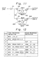
- Fig. 12 shows a set of parallel processing instructions (an assembler program) for performing the operation of the circuitry shown in Fig. 11.
- the first processing instruction series shown in Fig. 12 is a series of instructions relating to the data bus 4, and the second processing instruction series is a series of operation instructions.
- the signal data held in an input register (LIN1) in the interface 3a is transferred to a buffer memory (denoted by B in Fig. 12) 7 by a MOV instruction in the first processing instruction series.
- the transferred data is multiplied, at the multiplier 8, with coefficient data transferred to the buffer memory 9.
- the coefficient data is sequentially read-out from the RAM 10 at each step in accordance with the instruction signal from the sequence controller 18 and supplied to the buffer memory 9.
- the third step data issued from the multiplier 8 by the MTL instruction in the second processing instruction series is held in the accumulator (denoted by D1 in Fig. 12) 12a.
- the ALU 11 is in a state of allowing the output data of the multiplier 8 to pass through it.
- the multiplier 8 is provided with a shifter (not shown) in its output stage, and the data issued from the multiplier 8 becomes a result of multiplication by the data transferred to the buffer memory (B) 7 and the buffer memory 9 two steps before.
- data issued from the multiplier 8 is the result of multiplication by the data transfer performed in the first step.
- the signal data obtained by the third step described above corresponds to the output data of the multiplier 151 shown in Fig. 11.
- data in an off-set address $03 of the first signal data RAM (DRAM 1) 5 is read-out and transferred to the buffer memory (B) 7 by the MOV instruction in the first processing instruction series.
- the data issued from the multiplier 8 (corresponding to the output data of the multiplier 154 in Fig. 11) is added to the data held in the accumulator (D1) 12a by the MSM instruction in the second processing instruction series, and the resulting value is held in the accumulator (D2) 12b.
- the data held in the accumulator (D2) 12b corresponds to the output data of the adder 156 in Fig. 11.
- the data held in the accumulator (D2) 12b is transferred through the data bus 4 to an offset address $00 of the first signal data RAM (DRAM 1) 5 and written therein by the MOV instruction in the first processing instruction series.
- the data issued from the multiplier 8 (corresponding to the output data of the multiplier 155 in Fig. 11) is added to the data held in the accumulator (D2) 12b by the MSM instruction in the second processing instruction series, and the resulting summing value is held in the accumulator (D2) 12b.
- the MPX 13 relays the data held in the accumulator 12b to the ALU 11.
- the signal data held in the accumulator (D2) 12b corresponds to the output data of the multiplier 157 in Fig. 11.
- the data held in the accumulator (D2) 12b by the MOV instruction in the first processing instruction series is transferred to an output register (L01) in the interface 3a. Further, the data issued from the multiplier 8 (corresponding to the output data of the multiplier 259 in Fig. 11) is added to the data held in the accumulator (D1) 12a by the MSM instruction in the second processing instruction series, and the summing value is held in the accumulator (D1) 12a. In this case, the MPX 13 relays the data held in the accumulator 12a to the ALU 11. The data held in the accumulator (D1) 12a corresponds to the output data of the adder 261 in Fig. 11.
- the data held in the accumulator (D1) 12a is transferred through the data bus 4 written into an off-set address $02 of the first data RAM (DRAM 1) 5 by the MOV instruction in the first processing instruction series.
- the data issued from the multiplier 8 (corresponding to the output data of the multiplier 260 in Fig. 11) is added to the data held in the accumulator (D1) 12a by the MSM instruction in the second processing instruction series, and the result of addition is held in the accumulator (D1) 12a.
- the MPX 13 relays the data held in the accumulator 12a to the ALU 11.
- the signal data held in the accumulator (D1) 12a corresponds to the output data of the adder 262 in Fig. 11.
- the data held in the accumulator (D1) 12a is transferred to the output register (L02) in the interface 3b by the MOV instruction in the first processing instruction series.
- the data calculated in the third step is held in the accumulator (D1) 12a so that the data is again used in the operation in the fifth step. Furthermore, the data held in the accumulator (D1) 12a is used in the operation of the fourth step, and a result of operation is held in the accumulator (D2) 12b.
- the present value of the result obtained by the operation of arithmetic means is supplied to a plurality of accumulators for holding supplied data except at least one of the accumulators, the next value of the result of operation is supplied to the at least one of the accumulators, and data held in the accumulators other than the at least one of the accumulators is supplied to the arithmetic means. Therefore, when data of a result of operation is used for other plurality of operations as in the embodiment described above, the data of the result of operation is held in one of the accumulators, and other results of operations using the held data can be held in other accumulators.
Abstract
Description
- The present invention relates to an audio signal data processing system.
- There are known audio signal data processing systems capable of controlling the sound field by which a concert-hall (or theater) acoustic with reverberation and presence, for example, are created in a listening room or in an automobile. An example of such an audio data processing system is disclosed in Japanese Patent Application Laid Open No. 64-72615. In such audio signal processing systems, a DSP (digital signal processor) is provided for controlling the sound field by digitally processing an audio signal from an audio signal source such as a tuner. The DSP is constructed so that operating processes such as the four rules of arithmetic can be repeatedly performed at high speed.
- A plurality of the DSPs may be used simultaneously so that either a cascade processing or a parallel processing is selectively performed. For this type of processing, it has been conventionally necessary to provide a change-over switch outside the DSP, such as the change-over
switch 50 shown in Figure 1. Specifically, an input signal data is supplied to an input port IN of afirst DSP 51 and one of two stationary contacts of the change-over switch 50, and output data from an output port of the first DSP 51 is supplied to a first D/A converter (not shown) and the other stationary contact of the change-overswitch 50. Data selected by the change-over switch 50 is supplied to an input port IN of asecond DSP 52, and output data of the second DSP 52 is supplied to a second D/A converter (not shown) through its output port OUT. With this structure, when the change-over switch 50 is switched over to select the output data of thefirst DSP 51, the cascade processing is performed. When on the other hand, the change-over switch is switched over to select the input signal data, the parallel processing is performed. - As described above, for selectively performing the cascade processing and the parallel processing, there conventionally have been a necessity of providing a change-over switch and also a problem that the circuit construction becomes complicated for dealing with a time error generated between signal data respectively issued from each DSP in the case of the cascade processing. This is because timing signals must be separately prepared for the digital to analog conversion of each signal data in order to eliminate the time error.
- The DSPs are normally provided with multiplying means for multiplying coefficient data to the audio signal data. The audio signal data is stored in a data memory, and the audio signal is read-out in accordance with a predetermined program, and supplied to the multiplying means. The coefficient data, on the other hand, is stored in a coefficient memory, and sequentially read-out from the coefficient memory at executing timings of the above-described program, and in turn supplied to the multiplying means. When the data are supplied, the multiplying means executes multiplying operations according to the supplied data, and product data obtained by the multiplying operations are received by output means including an accumulator when required.
- Conventionally, the systems are configured so that, during a period in which the output means does not accept the product data, coefficient data having an initial value (1, for example) is read-out from the coefficient memory. However, when the data supplied from any one of the memories changes, it in turn causes on-off operations of gate circuits constituting the multiplying means. Thus, there has been a problem that the power consumption of the DSP increases during such periods.
- Furthermore, the DSP is provided with an accumulator for holding a result of operation of the arithmetic means, and data held in the accumulator is again supplied to the arithmetic means for the next accumulation operation, so that the accumulation operation is performed in the arithmetic means. With this structure, data is transferred in the DSP between memories or from a memory to the arithmetic means in accordance with a predetermined program, so that the arithmetic operation of signal data is repeatedly performed at high speed.
- However, with conventional audio signal data processing systems described above, there has been a problem that the number of program steps increases when a complex operating process is to be performed.
- An objective of the present invention is to provide an audio signal data processing system which selectively performs the cascade processing and parallel processing with a simple construction so that the necessity of providing a change-over switch or a timing adjusting circuit outside the DSP is eliminated.
- Another objective of the present invention is to provide an audio data processing system which is configured to reduce the power consumption when it does not need the product data of results of operations by the multiplying means.
- A further objective of the present invention is to provide an audio signal data processing system in which the number of program steps can be decreased as compared with conventional systems even when a complex operating process is performed.
- According to a first aspect of the present invention, the audio signal data processing system comprises first and second processing means respectively for processing audio signal data and having input and output ports of at least two channels, and control means for controlling the operation of the first and second processing means, wherein an input audio signal data is supplied to the input port of one channel of each of the first and second processing means, and output data from the output port of the one channel of the first processing means is supplied to the input port of the other channel of the second processing means, and output audio signal data are obtained at each output port of both channels of the second processing means.
- According to another aspect of the present invention, the audio signal data processing system comprises input means for sequentially supplying audio signal data, data memory control means for writing and reading-out the audio signal data into and from a data memory, a coefficient memory for storing coefficient data, coefficient memory control means for sequentially reading-out the coefficient data from the coefficient memory, multiplying means for multiplying the read-out audio signal data with the coefficient data, and output means for accepting product data obtained by a multiplying operation of the multiplying means and forwarding audio signal data corresponding to the product data in accordance with reading operations of the data memory control means and coefficient memory control means, wherein the same coefficient data is stored in locations of said coefficient memory from which data is read-out when the product data is not accepted by the output means.
- According to a further aspect of the present invention, the audio signal data processing system comprises input means for sequentially supplying audio signal data, data memory control means for writing and reading-out the audio signal data into and from a data memory, arithmetic means for multiplying the read-out audio signal data with predetermined coefficient data, holding means for accepting accumulation data as a result of operation of said arithmetic means and for holding said accumulation data, relaying means for supplying data held in said holding means to said arithmetic means for a next accumulating operation, and output means for forwarding signal data corresponding to the data held in the holding means, wherein the holding means includes a plurality of accumulators for holding data and selecting means for supplying a present value of said accumulation data to said plurality of accumulators except at least one of the accumulators and supplying a next value of said accumulation data to said at least one of the accumulators, and wherein said relaying means supplies data held in said plurality of accumulators other than said at least one of accumulators to said arithmetic means.
-
- Fig. 1 is a block diagram showing a conventional audio signal data processing system;
- Fig. 2 is a block diagram showing an embodiment of the present invention;
- Fig. 3 is a block diagram showing the DSP in the system of Fig. 2;
- Fig. 4 is a circuit diagram particularly showing a part of the system shown in Fig. 3;
- Fig. 5 is a flowchart showing the operation of a microcomputer in the system shown in Fig. 3;
- Fig. 6 is a block diagram showing another embodiment of the present invention;
- Fig. 7 is a block diagram showing a further embodiment of the present invention;
- Fig. 8 is a circuit diagram showing processing operations of the system shown in Fig. 7;
- Fig. 9 is a diagram showing a parallel processing instruction and coefficient data of each step for performing the operation of the circuit shown in Fig. 8;
- Fig. 10 is a block diagram showing a still further embodiment of the present invention;
- Fig. 11 is a circuit diagram showing processing operations of the system shown in Fig. 10;
- Fig. 12 is a diagram showing a parallel processing instruction and coefficient data of each step for performing the operation of the circuit shown in Fig. 11.
- Preferred embodiments of the present invention will be explained by way of example only and with reference to the accompanying drawings.
- In the audio signal data processing system shown in Figs. 2 and 3 as an embodiment of the present invention,
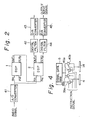
DSPs DSPs D converter 41. A first output port OUT₁ of the DSP 1 is connected to an input port IN₂ of theDSP 2. A D/Aconverter 43 is connected to an output port OUT₁ of theDSP 2 through adigital filter 42. Similarly, a D/A converter 45 is connected to an output port OUT₂ of theDSP 2 through adigital filter 44. - In the
DSP 1, the input signal data from the first input port IN₁ is supplied to an input/output interface 3a as shown in Fig. 3. Afirst data bus 4 is connected to the input/output interface 3a. Similarly, the input signal data from the second input port IN₂ is supplied to an input/output interface 3b which in turn is connected to thefirst data bus 4. As data memory for storing the audio signal data, twosignal data RAMs first data bus 4. Abuffer memory 7 is further connected to thedata bus 4, and the output-data of thebuffer memory 7 is connected to one of two inputs of amultiplier 8. Abuffer memory 9 for holding the coefficient data is connected to the other input of themultiplier 8. Acoefficient data RAM 10 for storing a plurality of coefficient data is further connected to thebuffer memory 9. An ALU (arithmetic logic unit) 11 is provided for executing operations such as the accumulation of the calculation output of themultiplier 8 which is supplied to one of two inputs of theALU 11. Anaccumulator 12 is provided for holding the calculation output of theALU 11, and its output is connected to the other input of theALU 11. The output of theaccumulator 12 is connected to thedata bus 4. - A
memory control circuit 31 is connected to thesignal data RAM 5. Thememory control circuit 31 generates a control signal for controlling the writing of data into a designated address of theRAM 5 and reading of data from designated address of theRAM 5. Amemory control circuit 32 like thememory control circuit 31 is connected to thesignal data RAM 6 via a change-overcircuit 33. The change-overcircuit 33 selectively transmits the control signal from thememory control circuit 31 or the control signal from thememory control circuit 32 so that operations of writing data into the designated address of the RAM and reading-out data from the designated address are performed in response to the control signal from thememory control circuit memory control circuit 34 like thememory control circuit 31 is connected to thecoefficient data RAM 10. - The
signal data RAM 6 is also connected to asecond data bus 14 which is independent from thefirst data bus 4. Specifically, there are provided a couple oftri-state buffers signal data RAM 6 and thefirst data bus 4 and a couple oftri-state buffers signal data RAM 6 and thesecond data bus 14, as illustrated in Fig. 4. Thebuffers sequence controller 18 which will be described later. For writing the signal data from thefirst data bus 4 into theRAM 6, thebuffer 39a turns on, and thebuffer 39b turns on when the signal data is read-out from theRAM 6 to thefirst data bus 4. Similarly, for writing the signal data from thedata bus 14 into theRAM 6, thebuffer 40a turns on, and thebuffer 40b turns on when the signal data is read-out from theRAM 6 to thesecond data bus 14. Thus, one of thetri-state buffers - An
interface 16 for the data transfer to and from anexternal RAM 15a is connected to thedata bus 14. The external RAM15a, which is a memory for the delay operation, is provided for producing a delay signal data of the audio signal data, and is capable of producing a signal data whose delay time is dependent on the memory capacity. Amemory control circuit 35 is provided for designating writing and reading addresses of theRAM 15, and a delaytime data RAM 17 is connected to thememory control circuit 35. The operations of writing and reading of the delay time data into and from theRAM 17 are controlled by amemory control circuit 38. - Operations of the
interfaces multiplier 8,buffer memories ALU 11,accumulator 12,memory control circuits over circuit 33 are controlled by thesequence controller 18. Aprogram RAM 19 is connected to thesequence controller 18, and thesequence controller 18 operates in accordance with the program stored in theprogram RAM 19. Aprogram counter 20 is connected to theprogram RAM 19, and every time the count value of theprogram counter 20 is incremented, an instruction code of the step corresponding to the new count value is read-out from theprogram RAM 19 and supplied to thesequence controller 18. To thesequence controller 18, also aregister 21 is connected for holding a plurality of commands from amicrocomputer 24 described later. - The
program RAM 19 and theregister 21 are respectively connected to amain bus 22. Themicrocomputer 24 is connected to themain bus 22 via aninterface 23. To themain bus 22, transfer buffers 26 and 27 are connected. Thetransfer buffer 26 temporarily holds the coefficient data supplied from themicrocomputer 24 for storing it in theRAM 10. Thetransfer buffer 27 temporarily holds the delay time data supplied from themicrocomputer 24 for storing it in theRAM 17. - The
microcomputer 24 is comprised of a microprocessor, RAM, ROM, and an interface (not shown). A keyboard is connected to themicrocomputer 24. Thekeyboard 25 is provided with a plurality of keys such as a plurality of mode keys for respectively designating a sound field mode, e.g. "hall 1", "hall 2" having different sound field characteristics, a frequency band setting key for controlling a graphic equalizer function, a level adjusting key, and a muting key (not shown). In the ROM of themicrocomputer 24, various programs and data are previously written. Those programs and data are, namely, a plurality of sequence control programs to be processed by thesequence controller 18, in addition to a DSP control program which is processed by themicrocomputer 24 itself, a plurality of coefficient data groups of initial reflective sound level, and a plurality of coefficient data groups for the first to fourth filters, both to be supplied to theRAM 10, and a plurality of delay time data groups to be supplied to theRAM 17 for setting the reading address. - In the
DSP 1, aclock generator 28 is provided, and clock pulses are supplied from theclock generator 28 to thesequence controller 18 and theprogram counter 20. The clock pulses generated by theclock generator 28 are also used as the timing signal of the A/D converter 41. - The audio signal data issued from the interface 3a is supplied to a first output port OUT₁ through a muting switch circuit 30a. The audio signal data issued from the
interface 3b is supplied to a second output port OUT₂ through a mutingswitch circuit 30b. The on-off control of the mutingswitch circuits 30a and 30b is performed by instruction signals issued from thesequence controller 18. - The
DSP 2 is constructed in the same manner as theDSP 1. Theinterface 23 of theDSP 2 is connected to themicrocomputer 24, and an external RAM like theexternal RAM 15a is also connected to theDSP 2. - In the structure of the
DSPs sequence controller 18 generates various instruction signals in addition to the instruction signals for thetri-state buffers 39a through 40b and the on-off control of the mutingswitch circuit 30a and 30b. Those instruction signals are, namely, instruction signal for transferring the coefficient data group held in thetransfer buffer 26 to theRAM 10, instruction signal for transferring the address data group held in thetransfer buffer 27 to theRAM 17, transfer instruction signal for transferring the audio signal data from theinterface 3 to the designated address of the signal data RAMs 5 and 6, instruction signal for reading-out the signal data from the designated address of thesignal data RAM buffer memory 7, instruction signal for reading-out the coefficient data from the designated address of theRAM 10 and transferring it to thebuffer memory 9, instruction signal for instructing various operations of theALU 11, transfer instruction signal for transferring the signal data held in theaccumulator 12 to the designated addresses of theRAMs buffer 7, transfer instruction signal for transferring data from the designated address of thesignal data RAM 6 to the designated writing address of theexternal RAM 15a, transfer instruction signal for transferring data from the designated delay address of theexternal RAM 15a to the designated address of thesignal data RAM 6, and reset instruction signal for initializing theRAMs external RAM 15a. These instruction signals are generated at appropriate timings according to commands from themicrocomputer 24 or the program stored in theRAM 19. Since the commands from themicrocomputer 24 are held in thecommand register 21, thesequence controller 18 generates an instruction signal corresponding to the command from themicrocomputer 24 by an interruption operation while monitoring the contents of thecommand register 21 during its operation according to the program. The command held in thecommand register 21 is canceled by thesequence controller 18 for example, when the corresponding instruction signal is generated. - When any one of the mode keys of the
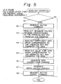
keyboard 25 is operated, as shown in Fig. 5 themicrocomputer 24 judges whether or not the operated key is a key for designating a sound field mode different from the sound field mode presently selected (step 41). When a sound field mode different from the present sound field mode is designated, themicrocomputer 24 immediately supplies the muting control instruction to thesequence controllers 18 of theDSPs switch circuits 30a and 30b for placing the system in a muting state (step 42). Then the microcomputer reads a sequence control program corresponding to the operated key, a coefficient data group α₁, α₂, ... ... αn, and a delay time data group t₁, t₂, ... ... tn from the ROM, and transfers them to theDSPs 1 and 2 (steps 43 through 45). The sequence control program is transferred to theRAM 19 through theinterface 23 and themain bus 22 of theDSPs RAM 19 by a memory writing control circuit (not shown). The coefficient data group is transferred to thetransfer buffer 26 through theinterface 23 and themain bus 22. The delay time data group is transferred to thetransfer buffer 27 through theinterface 23 and themain bus 22. After transferring the coefficient data and the delay time data to the transfer buffers 26 and 27 respectively, themicrocomputer 24 issues a data change-over command to thesequence controllers 18 of theDSPs 1 and 2 (step 46). Furthermore, themicrocomputer 24 issues an initialization command to the sequence controllers 18 (step 47). In response to the data change-over command, thesequence controller 18 issues a predetermined instruction signal to thememory control circuits transfer buffer 26 into a predetermined area of theRAM 10 and to write the delay time data group transferred to thetransfer buffer 27 into a predetermined area of theRAM 17. Furthermore, since thesequence controller 18 issues the above-mentioned reset instruction signal to thememory control circuits RAMs external RAM 15a by means of thememory control circuits - After the execution of the
step 47, themicrocomputer 24 issues a muting cancel command to thesequence controller 18, to turn-on the mutingswitch circuits 30a and 30b thereby canceling the muting state (step 48). More specifically, the muting switch circuits 30a and 30bare turned off only during a time period required for changing data or program in theRAM - When the parallel processing is designated by an operation of the
keyboard 25, themicrocomputer 24 places first channels of theDSPs DSPs keyboard 25, themicrocomputer 24 puts the first channels of theDSPs DSPs - Now the signal data processing operation within the
DSP 1 will be explained. The input audio signal supplied to the A/D converter 41 is converted to an audio signal data group d₁, d₂, ... ... dn at each of sampling timings synchronized with clock pulses from theclock generator 28. The audio signal data group is supplied to thefirst data bus 4 via the interface 3a. The signal data group supplied to thedata bus 4 is in turn supplied to theRAM - The signal data written in the
RAM 6 is sequentially transferred to an output register (not shown) in theinterface 16 via thedata bus 14, and from the output register further written into memory locations of theexternal RAM 15a designated by the writing address. The writing address is controlled by thememory control circuit 35, and one of a plurality of addresses whose number corresponds to the number of memory locations of theexternal RAM 15a is sequentially selected in a predetermined order each time the transferred signal data is supplied. In theexternal RAM 15a, the signal data in the memory location designated by the reading address is read-out, and transferred to an input register (not shown) in theinterface 16. Since the delay time data stored in theRAM 17 is read-out by thememory control circuit 38 and supplied to thememory control circuit 35, the reading address is set according to the delay time data supplied to thememory control circuit 35, using the writing address as a reference. In other words, the interval between the timing of writing a signal data into theRAM 15a and the timing of reading the same signal data becomes a delay time designated by the delay time data. The signal data transferred to the input register in theinterface 16 and held therein is in turn transferred to thesignal data RAM 6 via thedata bus 14. A delay audio signal data for controlling the sound field is produced by the transfer operation with theexternal RAM 15a described above. - The coefficient data read-out from the
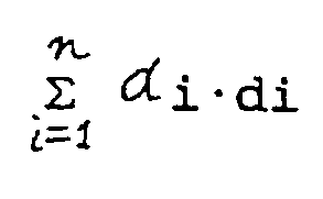
RAM 10 is supplied to thebuffer memory 9 and held therein. At timings appropriately determined by thesequence controller 18, the signal data is transferred to thebuffer memory 7 from theRAM accumulator 12. Therefore, themultiplier 8 executes the multiplication between the signal data held in thebuffer memory 7 and the coefficient data held in thebuffer memory 9. In the case of computing a sum of products between a signal data group d₁, d₂, ... ... dn and the coefficient data group α₁, α₂ ... ... αn for example, the following operations will be performed. At first, d₁ is held in thebuffer memory 7 for transmission, α₁ is held in thebuffer memory 9 for transmission, α₁·d₁ is calculated in themultiplier 8, and a "0" is added to α₁·d₁ at theALU 11. The result of this operation is held in theaccumulator 12. Subsequently, d₂ is held in thebuffer memory 7 for transmission, and α₂ is held in thebuffer memory 9 for transmission. At this time α₂·d₂ is calculated in themultiplier 8, α₁·d₁ is issued from theaccumulator 12, and α₁·d₁ + α₂·d₂ is calculated in theALU 11. By repeating these operations,
- In the above-description the processing operation for the first channel has been described. However, the same operation is performed for the second channel in the case of the cascade processing. Further, the data processing operation is performed in the similar manner in the
DSP 2. - The data passing operation in the parallel processing is such that the signal data group issued from the
interface 3b is supplied to theinterface 3b through thedata bus 4. - These operations are performed in response to instruction signals generated by the
sequence controller 18 according to the sequence control program stored in theprogram RAM 19. - In the embodiment described above, the clock generator is provided in each of the DSPs. However, the system may be arranged such that the clock pulses from one clock generator are supplied to each of the DSPs and the A/D converters.
- Furthermore, it is needless to mention that the input audio signal processed in the above-described apparatus may be either of a monaural signal or stereophonic audio signals.
- Fig. 6 shows a circuit connection for selectively performing the parallel processing and the cascade processing by three
DSPs 45 through 47. In this arrangement, theDSPs 45 through 47 respectively have three channels of input ports IN₁ through IN₃ and three channels of output ports OUT₁ through OUT₃. For performing the parallel processing, the first channel is placed into the data processing state, and the second and third channels are placed into the data passing state. For performing the cascade processing, on the other hand, the first through third channels are placed into the data processing state. - As specifically described in the foregoing, the first embodiment of the audio signal data processing system according to the present invention is configured such that the input audio signal data is supplied to input ports of one of channels in each of first and second processing means, the output data from an output port of the one of channels of the first processing means is supplied to an input port of the other channel of the second processing means, and the output audio signal data is obtained at output ports of both channels of the second processing means. Therefore, the cascade processing and the parallel processing can be selectively performed without using a change-over switch connected outside the processing means. Since the output signal data of each channel from the second processing means is forwarded as the processing output data in both of the cascade and parallel processing operations, generation of a timing error between signal data of different channels is prevented. This means that adjustment of timing during the conversion of the signal data to analog signals is made unnecessary so that the overall circuit construction can be simplified. Furthermore, in the case of operating the first and second processing means according to programs, there arises an advantageous effect that the same program can be commonly used in both of the first and second processing means.
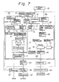
- Another embodiment of the present invention will be described with reference to Figs. 7 through 9 of the accompanying drawings. In this embodiment, the audio signal data processing system is as shown in Fig. 7 constructed substantially the same as the system shown in Fig. 3, and explanation of the same elements and corresponding parts will not be repeated. In this embodiment, however, a single input/
output interface 3 is connected to thedata bus 4, and the input audio signal is supplied to the input/output interface 3 through the A/D converter 41. Further, the clock pulses from theclock generator 28 are supplied to the A/D converter 41. In addition, themicrocomputer 24 in this embodiment also performs the operation shown in the flowchart of Fig. 5. - This embodiment of the audio signal data processing system having the
DSP 1 of the structure described above will be further described for a case in which a processing operation the same as that of a circuitry shown in Fig. 8 is performed. - In the circuitry shown in Fig. 8, input signal data is supplied to a
next circuit 153 through amultiplier 151 for multiplying the coefficient and a standard type first-orderIIR filter circuit 152. The first-orderIIR filter circuit 152 comprisesmultipliers adders delay element 158. Theadder 156 adds the signal data from themultiplier 151 and the signal data from themultiplier 154. The output data of themultiplier 156 is delayed by thedelay element 158 for one sampling period, and in turn supplied to themultipliers adder circuit 157 adds the signal data from theadder 156 and the signal data from themultiplier 155, and the resulting summing signal is supplied to thecircuit 153 as a filter output. - Fig. 9 shows a set of parallel processing instructions (an assembler program) for performing the operation of the circuitry shown in Fig. 8. The first processing instruction series shown in Fig. 9 is a series of instructions relating to the
data bus 4, and the second processing instruction series is a series of operation instructions. In the first step, the signal data held in an input register (LIN1) in theinterface 3 is transferred to a buffer memory (denoted by B in Fig. 9) 7 by a MOV instruction in the first processing instruction series. The transferred data is multiplied, at themultiplier 8, with coefficient data D₁ (corresponding to the coefficient of themultiplier 151 shown in Fig. 8) transferred to thebuffer memory 9. The coefficient data are written in theRAM 10 in the order shown in Fig. 9, and each coefficient data is read-out from theRAM 10 at each step in accordance with the instruction signal from thesequence controller 18 and supplied to thebuffer memory 9. - In the second step, data in an address $01 of the first signal data RAM 5 (DRAM 1) is read-out and transferred to the buffer memory (B) 7 by the MOV instruction in the first processing instruction series. At the same time, coefficient data D₂ is transferred from the
RAM 10 to thebuffer memory 9, and multiplied at themultiplier 8, with the signal data transferred to thebuffer memory 7. - In the third step, data issued from the
multiplier 8 by the MLT instruction in the second processing instruction series is held in the accumulator (denoted by D1 in Fig. 9) 12. In the case of the MTL instruction, theALU 11 is in a state of allowing the output data of themultiplier 8 to pass through it. Further, themultiplier 8 is provided with a shifter (not shown) in its output stage, to perform a level control operation by the shift of bits. In the case of the third step, the result of multiplication by the data transfer performed in the first step is used. The signal data obtained by the third step described above corresponds to the output data of themultiplier 151 shown in Fig. 8. In the third step, at the same time, coefficient data D₃ is transferred from theRAM 10 to thebuffer memory 9, and multiplied with the signal data transferred and held in thebuffer memory 7 in the step 2 (the second step). - In the fourth step, the data issued from the multiplier 8 (corresponding to the output data of the
multiplier 154 in Fig. 8) is added to the data held in the accumulator (D1) 12 by the MSM instruction in the second processing instruction series, and the resulting value is held in the accumulator (D1) 12. In this case, the data held in theaccumulator 12 is relayed to theALU 11. The data held in the accumulator (D1) 12 corresponds to the output data of theadder 156 in Fig. 8. In the fourth step also, the coefficient data D₃ is transferred from theRAM 10 to thebuffer memory 9, and multiplied in themultiplier 8 with the signal data transferred and held in thebuffer memory 7 in thestep 2. - In the fifth step, the data issued from the multiplier 8 (corresponding to the output data of the
multiplier 155 in Fig. 8) is added to the data held in the accumulator (D1) 12 by the MSM instruction in the second processing instruction series, and the resulting summing value is held in the accumulator (D1) 12. The data held in theaccumulator 12 is supplied to theALU 11. In this state, the signal data held in the accumulator (D1) 12 corresponds to the output data of themultiplier 157 in Fig. 8. In the fifth step also, the coefficient data D₃ is supplied from theRAM 10 to thebuffer memory 9, and in turn multiplied, in themultiplier 8, with the signal data transferred and held in thebuffer memory 7 in thestep 2. - In the sixth step, the data held in the accumulator (D1) 12 by the MOV instruction in the first processing instruction series is transferred, through the
data bus 4, to an address $00 of the signal data RAM (DRAM 1) 5 and the buffer memory (B) 7. This data is used as the input to thecircuit 153. If amultiplier 159 for multiplying the coefficient is provided in the input stage of thecircuit 153 as shown in Fig. 8, coefficient data D₄ (corresponding to the coefficient of the multiplier 159) is transferred from theRAM 10 to thebuffer memory 9, and multiplied with the signal data transferred to thebuffer memory 7 in themultiplier 8. - In the seventh step, data in an address $02 of the first data RAM (DRAM 1) 5, for example, is read-out by the MOV instruction of the first processing instruction series, and transferred to the buffer memory (B) 7. At the same time, coefficient data D₅ is transferred from the
RAM 10 to thebuffer memory 9, and multiplied in themultiplier 8 to the signal data transferred to thebuffer memory 7. - As specifically described in the foregoing, when the product data issued from the
multiplier 8 as multiplying means can be accepted by the output means such as theALU 11 or theaccumulator 12, the product data is used as the coefficient data of a new value, as in thesteps multiplier 8 is not accepted by theALU 11 or theaccumulator 12, data identical with the coefficient data of one step before is read-out, as in thesteps multiplier 8 is in a state of maintaining the multiplying operation of one step before. - In the other embodiment of the audio signal data processing system according to the present invention described above, the same coefficient data is held in the coefficient memory in areas from which reading is performed during periods when the product data is not accepted to the output means. Therefore the same coefficient data is read-out and supplied to the multiplying means during such periods. Accordingly, the operation of the multiplying means does not change if the signal data supplied to the multiplying means remains unchanged. This means that the on-off operation of the multiplying means does not occur in such a state, so that the electric power consumption of the system can be reduced. Also, there is a further advantage that the undesired radiation from the system is reduced.
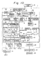
- A further embodiment of the present invention will be described with reference to Figs. 10 through 12 of the accompanying drawings. In this embodiment, the audio signal data processing system is as shown in Fig. 10 constructed substantially the same as the system shown in Fig. 3, and explanation of the same elements and corresponding parts will not be repeated. In this embodiment, however, an output signal of an MPX (multiplexer) 13 is connected to the other input of the
ALU 11. In accordance with instruction signals supplied from thesequence controller 18 which will be described later, theMPX 13 selectively supplies, to theALU 11, an output of one of threeaccumulators 12a through 12c for holding the calculation output of theALU 11. The input audio signal is supplied to the input/output interface 3a through the A/D converter 41. Further, the clock pulses from theclock generator 28 are supplied to the A/D converter 41. In addition, themicrocomputer 24 in this embodiment also performs the operation shown in the flowchart of Fig. 5. - This embodiment of the audio signal data processing system will be further described for a case in which a processing operation the same as that of a circuitry shown in Fig. 11 is performed.
- In the circuitry shown in Fig. 11, input signal data is supplied to standard type first-order
IIR filter circuits IIR filter circuits IIR filter circuit 152 comprisesmultipliers adders delay element 158. Theadder 156 adds the signal data from themultiplier 151 and the signal data from themultiplier 154. The output data of themultiplier 156 is delayed by thedelay element 158 for one sampling period, and in turn supplied to themultipliers adder circuit 157 adds the signal data from theadder 156 and the signal data from themultiplier 155, and the resulting summing signal is issued as a filter output. The first-orderIIR filter circuit 253 comprises, like the first-orderIIR filter circuit 152,multipliers adders delay elements 263. - Fig. 12 shows a set of parallel processing instructions (an assembler program) for performing the operation of the circuitry shown in Fig. 11. The first processing instruction series shown in Fig. 12 is a series of instructions relating to the
data bus 4, and the second processing instruction series is a series of operation instructions. In the first step, the signal data held in an input register (LIN1) in the interface 3a is transferred to a buffer memory (denoted by B in Fig. 12) 7 by a MOV instruction in the first processing instruction series. The transferred data is multiplied, at themultiplier 8, with coefficient data transferred to thebuffer memory 9. The coefficient data is sequentially read-out from theRAM 10 at each step in accordance with the instruction signal from thesequence controller 18 and supplied to thebuffer memory 9. - In the second step, data in an off-set address $01 of the first signal data RAM 5 (DRAM 1) is read-out and transferred to the buffer memory (B) 7 by the MOV instruction in the first processing instruction series.
- In the third step, data issued from the
multiplier 8 by the MTL instruction in the second processing instruction series is held in the accumulator (denoted by D1 in Fig. 12) 12a. In the case of the MLT instruction, theALU 11 is in a state of allowing the output data of themultiplier 8 to pass through it. Further, themultiplier 8 is provided with a shifter (not shown) in its output stage, and the data issued from themultiplier 8 becomes a result of multiplication by the data transferred to the buffer memory (B) 7 and thebuffer memory 9 two steps before. In the case of the third step, data issued from themultiplier 8 is the result of multiplication by the data transfer performed in the first step. The signal data obtained by the third step described above corresponds to the output data of themultiplier 151 shown in Fig. 11. - In the fourth step, data in an off-set address $03 of the first signal data RAM (DRAM 1) 5 is read-out and transferred to the buffer memory (B) 7 by the MOV instruction in the first processing instruction series. At the same time, the data issued from the multiplier 8 (corresponding to the output data of the
multiplier 154 in Fig. 11) is added to the data held in the accumulator (D1) 12a by the MSM instruction in the second processing instruction series, and the resulting value is held in the accumulator (D2) 12b. In this case, the data held in the accumulator (D2) 12b corresponds to the output data of theadder 156 in Fig. 11. - In the fifth step, the data held in the accumulator (D2) 12b is transferred through the
data bus 4 to an offset address $00 of the first signal data RAM (DRAM 1) 5 and written therein by the MOV instruction in the first processing instruction series. Also, the data issued from the multiplier 8 (corresponding to the output data of themultiplier 155 in Fig. 11) is added to the data held in the accumulator (D2) 12b by the MSM instruction in the second processing instruction series, and the resulting summing value is held in the accumulator (D2) 12b. In this case, theMPX 13 relays the data held in theaccumulator 12b to theALU 11. In this state, the signal data held in the accumulator (D2) 12b corresponds to the output data of themultiplier 157 in Fig. 11. - In the sixth step, the data held in the accumulator (D2) 12b by the MOV instruction in the first processing instruction series is transferred to an output register (L01) in the interface 3a. Further, the data issued from the multiplier 8 (corresponding to the output data of the
multiplier 259 in Fig. 11) is added to the data held in the accumulator (D1) 12a by the MSM instruction in the second processing instruction series, and the summing value is held in the accumulator (D1) 12a. In this case, theMPX 13 relays the data held in theaccumulator 12a to theALU 11. The data held in the accumulator (D1) 12a corresponds to the output data of theadder 261 in Fig. 11. - In the seventh step, the data held in the accumulator (D1) 12a is transferred through the
data bus 4 written into an off-set address $02 of the first data RAM (DRAM 1) 5 by the MOV instruction in the first processing instruction series. At the same time, the data issued from the multiplier 8 (corresponding to the output data of themultiplier 260 in Fig. 11) is added to the data held in the accumulator (D1) 12a by the MSM instruction in the second processing instruction series, and the result of addition is held in the accumulator (D1) 12a. In this case, theMPX 13 relays the data held in theaccumulator 12a to theALU 11. The signal data held in the accumulator (D1) 12a corresponds to the output data of theadder 262 in Fig. 11. - In the eighth step, the data held in the accumulator (D1) 12a is transferred to the output register (L02) in the
interface 3b by the MOV instruction in the first processing instruction series. - In the way described above, the data calculated in the third step is held in the accumulator (D1) 12a so that the data is again used in the operation in the fifth step. Furthermore, the data held in the accumulator (D1) 12a is used in the operation of the fourth step, and a result of operation is held in the accumulator (D2) 12b.
- As specifically described in the foregoing, in the further embodiment of the audio signal data processing system according to the present invention, the present value of the result obtained by the operation of arithmetic means is supplied to a plurality of accumulators for holding supplied data except at least one of the accumulators, the next value of the result of operation is supplied to the at least one of the accumulators, and data held in the accumulators other than the at least one of the accumulators is supplied to the arithmetic means. Therefore, when data of a result of operation is used for other plurality of operations as in the embodiment described above, the data of the result of operation is held in one of the accumulators, and other results of operations using the held data can be held in other accumulators. By this feature, it is made unnecessary to temporarily store a result of operation into the data memory or to repeat the same operation a plurality of times, so that the number of program steps can be reduced especially when a complex operating process is performed. Thus, the total execution time of the system can be reduced according to the present invention.
Claims (5)
first processing means for processing audio signal data;
second processing means for processing audio signal data, said first and second processing means having input and output ports of at least two channels; and
control means for controlling the operation of said first and second processing means, wherein an input audio signal data is supplied to the input port of one channel of each of said first and second processing means, and output data from the output port of said one channel of said first processing means is supplied to the input port of the other channel of said second processing means, and output audio signal data are obtained at each output port of both channels of said second processing means.
input means for sequentially supplying audio signal data;
data memory control means for writing and reading-out the audio signal data into and from a data memory;
a coefficient memory for storing coefficient data;
coefficient memory control means for sequentially reading-out the coefficient data from the coefficient memory;
multiplying means for multiplying the read-out audio signal data with the coefficient data; and
output means for accepting product data obtained by a multiplying operation of the multiplying means and forwarding audio signal data corresponding to the product data in accordance with reading operations of the data memory control means and coefficient memory control means, wherein the same coefficient data is stored in locations of said coefficient memory from which data is read-out when the product data is not accepted by the output means.
input means for sequentially supplying audio signal data;
data memory control means for writing and reading-out the audio signal data into and from a data memory;
arithmetic means for multiplying the read-out audio signal data with predetermined coefficient data;
holding means for accepting accumulation data as a result of operation of said arithmetic means and for holding said accumulation data;
relaying means for supplying data held in said holding means to said arithmetic means for a next accumulating operation; and
output means for forwarding signal data corresponding to the data held in the holding means, wherein the holding means includes a plurality of accumulators for holding data and selecting means for supplying a present value of said accumulation data to said plurality of accumulators except at least one of the accumulators and supplying a next value of said accumulation data to said at least one of the accumulators, and wherein said relaying means supplies data held in said plurality of accumulators other than said at least one of the accumulators to said arithmetic means.
Applications Claiming Priority (6)
| Application Number | Priority Date | Filing Date | Title |
|---|---|---|---|
| JP163322/89 | 1989-06-26 | ||
| JP1163328A JPH0328900A (en) | 1989-06-26 | 1989-06-26 | Audio signal data processor |
| JP163328/89 | 1989-06-26 | ||
| JP01163322A JP3083526B2 (en) | 1989-06-26 | 1989-06-26 | Audio signal data processing device |
| JP1163325A JPH0328897A (en) | 1989-06-26 | 1989-06-26 | Audio signal data processor |
| JP163325/89 | 1989-06-26 |
Publications (2)
| Publication Number | Publication Date |
|---|---|
| EP0405914A2 true EP0405914A2 (en) | 1991-01-02 |
| EP0405914A3 EP0405914A3 (en) | 1992-12-16 |
Family
ID=27322144
Family Applications (1)
| Application Number | Title | Priority Date | Filing Date |
|---|---|---|---|
| EP19900306982 Withdrawn EP0405914A3 (en) | 1989-06-26 | 1990-06-26 | Audio signal data processing system |
Country Status (2)
| Country | Link |
|---|---|
| US (1) | US5091951A (en) |
| EP (1) | EP0405914A3 (en) |
Cited By (1)
| Publication number | Priority date | Publication date | Assignee | Title |
|---|---|---|---|---|
| EP1986102A2 (en) | 2007-03-23 | 2008-10-29 | Siemens Audiologische Technik GmbH | Processor system with directly controllable ports |
Families Citing this family (17)
| Publication number | Priority date | Publication date | Assignee | Title |
|---|---|---|---|---|
| KR920009641B1 (en) * | 1990-08-09 | 1992-10-22 | 삼성전자 주식회사 | Digital audio equalizer |
| JP2680483B2 (en) * | 1991-05-02 | 1997-11-19 | 株式会社東芝 | Digital signal processor |
| US5410603A (en) * | 1991-07-19 | 1995-04-25 | Casio Computer Co., Ltd. | Effect adding apparatus |
| JP3088035B2 (en) * | 1991-12-18 | 2000-09-18 | パイオニアビデオ株式会社 | Digital signal processor |
| JPH0821833B2 (en) * | 1992-07-28 | 1996-03-04 | インターナショナル・ビジネス・マシーンズ・コーポレイション | Circuit for filtering digital audio information and method for producing a filtered digital signal |
| DE69617480T2 (en) * | 1995-01-13 | 2002-10-24 | Yamaha Corp | Device for processing a digital sound signal |
| GB2299422B (en) * | 1995-03-30 | 2000-01-12 | Sony Uk Ltd | Object code allocation in multiple processor systems |
| US5758177A (en) * | 1995-09-11 | 1998-05-26 | Advanced Microsystems, Inc. | Computer system having separate digital and analog system chips for improved performance |
| US5797028A (en) * | 1995-09-11 | 1998-08-18 | Advanced Micro Devices, Inc. | Computer system having an improved digital and analog configuration |
| JP3620264B2 (en) * | 1998-02-09 | 2005-02-16 | カシオ計算機株式会社 | Effect adding device |
| JP3946444B2 (en) * | 1998-05-14 | 2007-07-18 | ルミネックス コーポレイション | Configuration and method for zero dead time of flow cytometer |
| US7678986B2 (en) * | 2007-03-22 | 2010-03-16 | Qualcomm Incorporated | Musical instrument digital interface hardware instructions |
| US7663051B2 (en) * | 2007-03-22 | 2010-02-16 | Qualcomm Incorporated | Audio processing hardware elements |
| TWI337339B (en) * | 2007-06-23 | 2011-02-11 | Princeton Technology Corp | Audio process system |
| CN101359471B (en) * | 2007-08-01 | 2012-11-28 | 普诚科技股份有限公司 | Audio processing system |
| CN101692170B (en) * | 2009-10-16 | 2013-01-09 | 北京联合大学生物化学工程学院 | Serial D/A converter circuit shared by two singlechips |
| JP6362456B2 (en) * | 2014-07-09 | 2018-07-25 | ローム株式会社 | Motor drive circuit, cooling device using the same, and electronic device |
-
1990
- 1990-03-01 US US07/486,866 patent/US5091951A/en not_active Expired - Lifetime
- 1990-06-26 EP EP19900306982 patent/EP0405914A3/en not_active Withdrawn
Non-Patent Citations (6)
| Title |
|---|
| ELECTRO/87 AND MINI/MICRO NORTHEAST 12TH CONFERENCE RECORD; IEEE COMP.SOC.PRESS, NEW YORK, US 1987, LOS ANGELES, US pages 1 - 7 F.FERRO, K.ULERY 'THE ARCHITECTURE AND PROGRAMMING OF THE WE DSP16 DIGITAL SIGNAL PROCESSOR' * |
| ELEKTRONIK vol. 35, no. 18, September 1986, FRANZIS VERLAG GMBH MÜNCHEN, DE pages 149 - 156 P.ECKELMANN 'VORTEILE DES KASKADIERBAREN SIGNALPROZESSORS' * |
| IEEE 1988 INTERNATIONAL CONF. ON CONSUMER ELECTRONICS, IEEE COMP.SOC.PRESS, NEW YORK, US 8 June 1988, ROSEMONT, ILLINOIS, US pages 224 - 225 OSAMU IKEDA ET AL 'A DIGITAL SIGNAL PROCESSOR FOR DIGITAL AUDIO USE' * |
| IEEE 1989 INT. CONF. ON CONSUMER ELECTRONICS, IEEE COMP.SOC.PRESS, NEW YORK, US 6 June 1989, ROSEMONT, ILLINOIS, US pages 150 - 151 YOSHINORI MATSUSHITA ET AL 'A 32/24 BIT DIGITAL AUDIO SIGNAL PROCESSOR' * |
| IEEE TRANSACTIONS ON CONSUMER ELECTRONICS vol. 33, no. 4, November 1987, IEEE COMP.SOC.PRESS, NEW YORK, US pages 507 - 511 P.ANDERS, P.ASLETT 'A MONOLITHIC INTEGRATED DIGITAL SIGNAL PROCESSOR FOR HIFI AUDIO APPLICATIONS' * |
| PHILIPS TECHNICAL REVUE, ADM.PTR. PHILIPS NATUURKUNDING LABORATORIUM, EINDHOVEN, NL vol. 42, no. 6/7, April 1986, pages 201 - 216 E.H.J.PERSOON , C.J.B. VANDENBULCKE 'DIGITAL AUDIO: EXAMPLES OF THE APPLICATION OF THE ASP INTEGRATED SIGNAL PROCESSOR' * |
Cited By (2)
| Publication number | Priority date | Publication date | Assignee | Title |
|---|---|---|---|---|
| EP1986102A2 (en) | 2007-03-23 | 2008-10-29 | Siemens Audiologische Technik GmbH | Processor system with directly controllable ports |
| EP1986102A3 (en) * | 2007-03-23 | 2009-02-04 | Siemens Audiologische Technik GmbH | Processor system with directly controllable ports |
Also Published As
| Publication number | Publication date |
|---|---|
| US5091951A (en) | 1992-02-25 |
| EP0405914A3 (en) | 1992-12-16 |
Similar Documents
| Publication | Publication Date | Title |
|---|---|---|
| US5218710A (en) | Audio signal processing system having independent and distinct data buses for concurrently transferring audio signal data to provide acoustic control | |
| US5091951A (en) | Audio signal data processing system | |
| US5210806A (en) | Digital audio signal processing apparatus | |
| JP2639543B2 (en) | Digital filter device | |
| US5179531A (en) | Accelerated digital signal processor | |
| EP0487181B1 (en) | Sound field compensating apparatus | |
| EP0405915B1 (en) | Audio signal data processing system | |
| JPH0812657B2 (en) | Data storage | |
| US5255323A (en) | Digital signal processing device and audio apparatus using the same | |
| US6330338B1 (en) | Process and device for mixing digital audio signals | |
| US5754874A (en) | Digital signal processor with selective sound operation | |
| JP3083526B2 (en) | Audio signal data processing device | |
| JP3120483B2 (en) | Effect adding device | |
| JPH0328897A (en) | Audio signal data processor | |
| JPH0328899A (en) | Audio signal data processor | |
| JPH0328900A (en) | Audio signal data processor | |
| US5305439A (en) | Method and apparatus for time-shared processing of different data word sequences | |
| JPH0321998A (en) | Audio signal data processor | |
| JPH0631996B2 (en) | Audio signal data processor | |
| KR0175399B1 (en) | Data Controllers in Oversampling Digital Filters | |
| JP3428149B2 (en) | Digital signal processor | |
| JPH0328896A (en) | Audio signal data processor | |
| JPH02250420A (en) | Filter coefficient revision system for digital filter | |
| JPH0328893A (en) | Audio signal data processor | |
| JPH031198A (en) | Digital signal processor |
Legal Events
| Date | Code | Title | Description |
|---|---|---|---|
| PUAI | Public reference made under article 153(3) epc to a published international application that has entered the european phase |
Free format text: ORIGINAL CODE: 0009012 |
|
| AK | Designated contracting states |
Kind code of ref document: A2 Designated state(s): DE FR GB |
|
| PUAL | Search report despatched |
Free format text: ORIGINAL CODE: 0009013 |
|
| AK | Designated contracting states |
Kind code of ref document: A3 Designated state(s): DE FR GB |
|
| 17P | Request for examination filed |
Effective date: 19930108 |
|
| 17Q | First examination report despatched |
Effective date: 19951127 |
|
| STAA | Information on the status of an ep patent application or granted ep patent |
Free format text: STATUS: THE APPLICATION IS DEEMED TO BE WITHDRAWN |
|
| 18D | Application deemed to be withdrawn |
Effective date: 20020103 |