EP0406900B1 - Driving circuit for liquid crystal display apparatus - Google Patents
Driving circuit for liquid crystal display apparatus Download PDFInfo
- Publication number
- EP0406900B1 EP0406900B1 EP90112963A EP90112963A EP0406900B1 EP 0406900 B1 EP0406900 B1 EP 0406900B1 EP 90112963 A EP90112963 A EP 90112963A EP 90112963 A EP90112963 A EP 90112963A EP 0406900 B1 EP0406900 B1 EP 0406900B1
- Authority
- EP
- European Patent Office
- Prior art keywords
- signal
- liquid crystal
- alternating signal
- driver
- line
- Prior art date
- Legal status (The legal status is an assumption and is not a legal conclusion. Google has not performed a legal analysis and makes no representation as to the accuracy of the status listed.)
- Expired - Lifetime
Links
Images


Classifications
-
- G—PHYSICS
- G09—EDUCATION; CRYPTOGRAPHY; DISPLAY; ADVERTISING; SEALS
- G09G—ARRANGEMENTS OR CIRCUITS FOR CONTROL OF INDICATING DEVICES USING STATIC MEANS TO PRESENT VARIABLE INFORMATION
- G09G3/00—Control arrangements or circuits, of interest only in connection with visual indicators other than cathode-ray tubes
- G09G3/20—Control arrangements or circuits, of interest only in connection with visual indicators other than cathode-ray tubes for presentation of an assembly of a number of characters, e.g. a page, by composing the assembly by combination of individual elements arranged in a matrix no fixed position being assigned to or needed to be assigned to the individual characters or partial characters
- G09G3/34—Control arrangements or circuits, of interest only in connection with visual indicators other than cathode-ray tubes for presentation of an assembly of a number of characters, e.g. a page, by composing the assembly by combination of individual elements arranged in a matrix no fixed position being assigned to or needed to be assigned to the individual characters or partial characters by control of light from an independent source
- G09G3/36—Control arrangements or circuits, of interest only in connection with visual indicators other than cathode-ray tubes for presentation of an assembly of a number of characters, e.g. a page, by composing the assembly by combination of individual elements arranged in a matrix no fixed position being assigned to or needed to be assigned to the individual characters or partial characters by control of light from an independent source using liquid crystals
- G09G3/3611—Control of matrices with row and column drivers
- G09G3/3622—Control of matrices with row and column drivers using a passive matrix
-
- G—PHYSICS
- G09—EDUCATION; CRYPTOGRAPHY; DISPLAY; ADVERTISING; SEALS
- G09G—ARRANGEMENTS OR CIRCUITS FOR CONTROL OF INDICATING DEVICES USING STATIC MEANS TO PRESENT VARIABLE INFORMATION
- G09G3/00—Control arrangements or circuits, of interest only in connection with visual indicators other than cathode-ray tubes
- G09G3/20—Control arrangements or circuits, of interest only in connection with visual indicators other than cathode-ray tubes for presentation of an assembly of a number of characters, e.g. a page, by composing the assembly by combination of individual elements arranged in a matrix no fixed position being assigned to or needed to be assigned to the individual characters or partial characters
- G09G3/34—Control arrangements or circuits, of interest only in connection with visual indicators other than cathode-ray tubes for presentation of an assembly of a number of characters, e.g. a page, by composing the assembly by combination of individual elements arranged in a matrix no fixed position being assigned to or needed to be assigned to the individual characters or partial characters by control of light from an independent source
- G09G3/36—Control arrangements or circuits, of interest only in connection with visual indicators other than cathode-ray tubes for presentation of an assembly of a number of characters, e.g. a page, by composing the assembly by combination of individual elements arranged in a matrix no fixed position being assigned to or needed to be assigned to the individual characters or partial characters by control of light from an independent source using liquid crystals
- G09G3/3611—Control of matrices with row and column drivers
- G09G3/3614—Control of polarity reversal in general
Definitions
- the present invention relates to a driving circuit for a liquid crystal display apparatus comprising: a segment driver for sequentially outputting, line by line, picture element data into a plurality of parallell electrodes contacting a liquid crystal in a first direction; a common driver for sequentially outputting scanning pulses in a line by line direction into a plurality of parallell electrodes contacting the liquid crystal in a second direction being perpendicular to the first direction, wherein picture elements are formed at electrode intersections; and alternating signal generating means for inverting at constant time periods the polarity of the picture element data and the scanning pulses with an alternating signal so as to drive the respective liquid crystal.
- Such a driving circuit is known from Patent Abstracts of Japan, Vol. 13, No.347 (P-910), 04.08.89 and JP-A-11006017.
- electroylsis is caused in the liquid crystal, when the direct current voltages is continuously applied upon the liquid crystal which becomes each picutre element, to shorten the service life.
- the polarities of the voltage signals corresponding to the picture element data, namely the scanning pulses are inverted, applied upon one, the other electrodes grasping liquid crystal for each of given periods (for example, one frame scanning time) by the alternating signals so as to turn the average voltage to be applied upon the liquid crystal into zero.
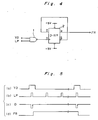
- the above described alternating signal is conventionally generated by an alternating signal generating circuit composed of a NAND gate 1 and a D-flip-flop 2 shown in Fig. 4.
- the NAND gate 1 receives a frame scanning start signal YD (see Fig. 5(a)) to be inputted at each scanning start of one frame, and the latch pulse LP (see Fig. 5 (b)) to be inputted at each latching of the picture element data of one line portion to invert the logical product of both the signals for outputting the set signal D (see Fig. 5(c)) into the D-flip-flop 2.
- the D-flip-flop 2 outputs into an output terminal Q through a reset terminal D the signal of an inverting output terminal Q at each rising of the set signal D to get such an alternating signal FR as shown in Fig. 5(d).
- Fig. 6 shows a driving circuit for a simple matrix type liquid crystal display apparatus of the conventional multiduty adopting a system of reversing the polarities of the picture element data, scanning pulses by the above described alternating signal FR.
- the driving circuit is composed of a segment driver 12 for sequentially outputting one line portion by one line portion the picture element data into the one longitudinal direction of seven line shaped electrode grasping the liquid crystal matrix 11 which composes the thirty five picture elements of 5 X 7, and a common driver 13 for sequentially outputting in a row direction the scanning pulses into the other lateral direction five line shaped electrode grasping above described the liquid crystal.
- the binary (“0",”1") picture element data D1, ..., D7 of seven per line are synchronized with a clock XCK, is accommodated into the shift register 14 of the segment driver 12, and is retained for one horizontal scanning period into a data latch 15 receiving the latch pulse LP.
- a level converter 16 and an analog switch 17 composed of many transistors adjust in level, convert seven input signals of "0” or “1” from the data latch 15 into four operation voltage values V5, V0; V3, V2 to be selected by the voltage value selection switches 18, 19 in accordance with the "H", "L” of the alternating signal FR by on signal, off signal so as to effect parallel output into the one seven line shaped electrodes.
- the shift register 20 of the common driver 13 synchronizes into the latch pulse LP to be inputted for each one horizontal scanning operation the frame scanning start signal YD to be inputted at the scanning start time of one frame so as to shift it.
- the data latch 21 retains the shifted pulse signal for one horizontal scanning period.
- the level converter 22 and the analog switch 23 composed of many transistors adjust in level, convert the five input signals of "0" or "1” from the data latch 21 into four operation voltage values V0, V5; V4, V1 to be selected respectively by the voltage value selection switches 24, 25 in accordance with the "H", "L” of the alternating signal FR from the on signal, off signal so as to effect parallel output into the other five line shaped electrodes.
- the scanning pulses V0, V5 are sequentially scanned from top to bottom like Ca, Cb, ... into the five lateral direction line shaped electrodes by the common driver 13.
- the common driver 13 Among the line liquid crystal with the scanning pulses being fed into it, only the liquid crystal with the white level signals V5, V0 being fed into it by the segment driver 12 is displayed.
- Fig. 7 is a view showing across a period of two frames the electrode wave forms to be outputted respectively from the above-described analog switches 17, 23 into both electrodes grasping the electrode by way of the liquid crystal of Cb line S2 row on the picture face.
- the frame scanning start signal YD is outputted as a pulse signal into each frame scanning start time.
- the latch pulse LP is outputted five times, setting each horizontal scanning in one frame.
- the D-flip-flop 2 outputs the alternating signal FR which is varied into "H", "L” for each one frame as described hereinabove (see Figs. 4, 5) in accordance with both the pulses.
- the analog switch 17 on the side of the segment driver 12 outputs a black level voltage signal of V3 when the FR is "H” as shown in Fig. 7(d), a black level voltage signal of V2 when the FR is “L”, outputs a white level voltage signal of V5 when the FR is "H”, a white level voltage signal of V0 when the FR is "L".
- the respective No. 2 line, No. 4 line of the first, second frames become white levels.
- the analog switch 23 on the side of the common driver 13 outputs a non-selection level voltage signal of V4 when the FR is the "H", a non-selection level voltage signal of V1 when the FR is the “L”, outputs a selection level voltage signal of V0 when the FR is the "H”, a selection level voltage signal of V5 when the FR is "L”.
- the Cb line becomes the selection level, being set to the second latch pulse LP for a period of scanning the Cb line which is the No. 2 line in the first, second frames. Since the voltage signals like Fig.
- liquid crystal 7 (d), (e) are applied respectively upon both the electrodes grasping the liquid crystal of the Cb line, the S2 row, the potential difference to be added to the liquid crystal is provided as in Fig. 7(f).
- the above described liquid crystal is to light (display) with voltage
- the picture face of the liquid crystal display apparatus becomes larger, and the wave forms of the output voltage signal from both the drivers 12, 13 shown in Fig. 7 (f) become duller when the liquid crystal picture elements to be driven are increased to increase the load.
- the duller wave forms appear considerably (see Fig. 8(c)) when the alternating signal FR changes from the "L" to the "H” or from the "H” to the “L” as shown in Fig. 8(d).
- the output voltage signal from the common driver 13 is much duller.
- the non-selection level voltage to be outputted from the common driver 13 changes from V1 to V4.
- the voltage Ca of the No. 1 line has become V0 in the selection level only for the horizontal scanning period, it returns to the V4 in the non-selection level. Since the voltage variation from the V1 of the voltage Ca to the V0 is small, the circular arc shaped dullness of the wave form corner portion is small, and the voltage variation from the V0 to the V4 is larger, so that the circular arc dullness of the wave form corner portion is larger.
- the liquid crystal driving voltage which is the output potential difference of the common driver 13 and the segment driver 12, at the inversion time of the alternating signal FR, works in a direction of lowering the potential difference with the dullness of the Ca and the Lb being mutually opposite in direction on the No. 1 line, is not lowered so much in the potential difference with the dullness of the Cb and the Lb being mutually the same in direction on the No.
- the horizontal string shows in the constant value of the turbulent picture face of the effective value of the driving signal affected by the variation in the alternating signal FR, with a defect that the display quality is degraded.
- the driving circuit known from the above cited Abstracts of Japan, Vo. 13, No. 347 (P-910), 04.08.89 and JP-A-11006017 includes additional triggering circuitry to trigger a polarity switching circuit for generating a signal for switching the polarity of a liquid crystal driving voltage.
- Said triggering signal generating circuitry generates a signal which is synchronized with a delay clock for outputting the signal as a polarity switching signal.
- a display inhibiting signal is generated for a period of two cycles of the delay clock after the switching of the polarity of the signal FR, a frequency division signal put into the triggering signal generating circuit as inhibited by a NAND circuit in the period to stop the triggering signal generating operation.
- the display inhibiting signal is put into a scanning electrode driving IC, and then all scanning outputs have a waveform of non-selection.
- the object of the present invention is to provide a driving circuit for a liquid crystal display apparatus which can avoid a turbulence effected by each inversion of the driving voltage wherein additional circuitry for trigger signal generation should not be required.
- a driving circuit for a liquid crystal display apparatus which is characterized in that the common driver includes a plurality of cascade connected driver stages , wherein a frame scanning start signal is adapted to be sequentially inputted to a first stage of each cascade connected driver at a time interval corresponding to a certain number of latch pulses, said number of latch pulses being a few latch pulses intervals more than a number of actual display lines driven by each cascade connected driver.
- the pulse signal for the cascade connection use is outputted into the alternating signal generating means from the driver.
- the alternating signal generating means is delayed by a few latch pulse intervals from the input of the above described pulse signal to risingly invert the alternating signal into the "H" to output it into the common driver and the segment driver. Since the next frame scanning start signal is not yet inputted yet into the common driver although the scanning pulse and picture element data to be outputted respectively from both the drivers are inverted in their polarity, the display of the next frame is not yet performed by the liquid crystal matrix.
- the liquid crystal matrix is driven sequentially from the uppermost line as described hereinabove by the reverse polarity of voltage corresponding to the difference of the scanning pulse and the picture element data to effect the lighting operation. Since the polarity of the scanning pulse and the picture element data within the non-display region is reversed, the turbulence of the driving voltage accompanied by the reversion does not appear on the display picture face. Thereby the display quality is prevented to become degraded.
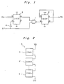
- Fig. 1 a block diagram showing one embodiment of an alternating signal generating circuit to be used in the driving circuit of a liquid crystal display according to one preferred embodiment of the present invention.
- the alternating signal generating circuit has a D-flip-flop 3 provided in the front stage of the NAND gate 1 of the circuit described in Fig. 4.
- a pulse signal Di0 for cascade connection use to be outputted from the common driver to be described is inputted into the reset terminal D
- a latch pulse LP is inputted through the inverter 4 into the set terminal D.
- the output Q of the D-flip-flop 3 is inputted into one input terminal of the NAND gate 1, the above described latch pulse LP is inputted into the other input terminal of the NAND gate 1.
- the above described driving circuit is the same in construction as in Fig. 6, the common driver 13 of the driving circuit described in Fig. 6 is constructed with n number of drivers 6, 6, ... being cascade connected shown as in Fig. 2, with an exception that a period of the frame scanning start signal YD to be inputted into the driver 6 of the uppermost stage is assumed to have the time corresponding to eight latch pulses which are more by three than the number five of the actual display lines Ca through Ce as shown in Fig. 3(a).
- the common driver is synchronized with the latch pulse LP of Fig. 3(c) sequentially from the driver 6 of the uppermost stage with the alternating signal FR being "L" (see Fig. 3 (d)) so as to sequentially output the scanning pulse VO of the positive polarity sequentially from the top like Ca, cb, ... into five line shaped electrodes in the line direction of the liquid crystal matrix 11.
- the segment driver 12 is synchronized with the latch pulse LP to sequentially output one line portion of the positive polarity of picture elements data V3, V5 sequentially from the uppermost line into seven line shaped electrodes in the row direction.
- the respective liquid crystal is driven with the positive polarity of voltage equivalent to the difference of the scanning pulse and the picture element data so as to sequentially effect the lighting operation from the uppermost line.
- the pulse signal Di0 for the cascade connection is outputted at such a timing as shown in the broken line of Fig. 3(b) from the driver 6 to the D-flip-flop 3 of the alternating signal generating circuit.
- the pulse signal Di0 inputted into the terminal D is latched into the D-flip-flop 3 with the falling of the sixth latch pulse LP, and is inputted into the NAND gate 1 as an output Q delayed by one latch pulse portion as shown in the solid line of Fig. 3(b). Since the NAND gate 1 and the D-flip-flop 2 operate in the same way as described in Fig. 5, the alternating signal FR which is the output of the D-flop-flop 2 is caused to be reversed into the "H" with the falling of the seventh latch pulse LP. Thereafter, the eighth latch pulse LP is inputted, the next latch pulse becomes a first latch pulse of the second frame, and at the same time, the second frame scanning start signal YD is inputted as in Fig. 3(a).
- the region becomes an interior N of the non-display region where no display is effected on the liquid crystal matrix 11, with the above described quality degraded region M being provided between one latch pulses before and after the reversion of the alternating signal FR within it.
- the same thing can be said about the reversion to the "L” from "H” of the alternating signal FR by the seventh latch pulse of the second frame, with the display quality degradation region M′ by the reversion being also included in the non-display region N′.
- the turbulence of the driving voltage accompanied by the reversion does not show, thus resulting in no degradation in the display quality.
- the pulse signal Di0 for cascade connection use from the lowermost stage of the common driver 5 is used as the trigger signal of the reversion of the alternating signal FR, the circuit for trigger signal generation use is not required to be especially provided.
- the non-display regions N, N′ are made too wide in width, the duty of the latch pulse becomes higher, the effective value difference in driving voltage signal between on and off becomes smaller, so that the contrast of the display becomes worse. It is desired that the latch pulse be restrained into the 2 through 4 latch pulse portions.
- the pulse signal Di0 for cascade connection use is delayed by one latch pulse portion by the use of the D-flip-flop 3, but the pulse signal Di0 may be latched between the one latch pulse on the common driver itself and may be inputted, instead of the frame scanning start signal YD of the NAND gate 1 of Fig. 4.
- a common driver which sequentially drives and outputs in the row direction the scanning pulses into the other electrode grasping the liquid crystal of a simple matrix type is composed of a plurality of drivers cascade connected.
- the frame scanning start signal is inputted, at a time interval corresponding to latch pulses which are more by a few pulses than the number of the actual display lines, into the common driver.
Description
- The present invention relates to a driving circuit for a liquid crystal display apparatus comprising: a segment driver for sequentially outputting, line by line, picture element data into a plurality of paralell electrodes contacting a liquid crystal in a first direction; a common driver for sequentially outputting scanning pulses in a line by line direction into a plurality of paralell electrodes contacting the liquid crystal in a second direction being perpendicular to the first direction, wherein picture elements are formed at electrode intersections; and alternating signal generating means for inverting at constant time periods the polarity of the picture element data and the scanning pulses with an alternating signal so as to drive the respective liquid crystal.
- Such a driving circuit is known from Patent Abstracts of Japan, Vol. 13, No.347 (P-910), 04.08.89 and JP-A-11006017.
- Generally, in the simple matrix type liquid crystal display apparatus of a multiduty, electroylsis is caused in the liquid crystal, when the direct current voltages is continuously applied upon the liquid crystal which becomes each picutre element, to shorten the service life. The polarities of the voltage signals corresponding to the picture element data, namely the scanning pulses are inverted, applied upon one, the other electrodes grasping liquid crystal for each of given periods (for example, one frame scanning time) by the alternating signals so as to turn the average voltage to be applied upon the liquid crystal into zero.
- The above described alternating signal is conventionally generated by an alternating signal generating circuit composed of a
NAND gate 1 and a D-flip-flop 2 shown in Fig. 4. Namely, theNAND gate 1 receives a frame scanning start signal YD (see Fig. 5(a)) to be inputted at each scanning start of one frame, and the latch pulse LP (see Fig. 5 (b)) to be inputted at each latching of the picture element data of one line portion to invert the logical product of both the signals for outputting the set signal D (see Fig. 5(c)) into the D-flip-flop 2. The D-flip-flop 2 outputs into an output terminal Q through a reset terminalD the signal of an inverting output terminalQ at each rising of the set signal D to get such an alternating signal FR as shown in Fig. 5(d). - Fig. 6 shows a driving circuit for a simple matrix type liquid crystal display apparatus of the conventional multiduty adopting a system of reversing the polarities of the picture element data, scanning pulses by the above described alternating signal FR. The driving circuit is composed of a
segment driver 12 for sequentially outputting one line portion by one line portion the picture element data into the one longitudinal direction of seven line shaped electrode grasping theliquid crystal matrix 11 which composes the thirty five picture elements of 5X 7, and acommon driver 13 for sequentially outputting in a row direction the scanning pulses into the other lateral direction five line shaped electrode grasping above described the liquid crystal. The binary ("0","1") picture element data D1, ..., D7 of seven per line are synchronized with a clock XCK, is accommodated into theshift register 14 of thesegment driver 12, and is retained for one horizontal scanning period into adata latch 15 receiving the latch pulse LP. Alevel converter 16 and an analog switch 17 composed of many transistors adjust in level, convert seven input signals of "0" or "1" from thedata latch 15 into four operation voltage values V5, V0; V3, V2 to be selected by the voltagevalue selection switches - The
shift register 20 of thecommon driver 13 synchronizes into the latch pulse LP to be inputted for each one horizontal scanning operation the frame scanning start signal YD to be inputted at the scanning start time of one frame so as to shift it. Thedata latch 21 retains the shifted pulse signal for one horizontal scanning period. Thelevel converter 22 and theanalog switch 23 composed of many transistors adjust in level, convert the five input signals of "0" or "1" from thedata latch 21 into four operation voltage values V0, V5; V4, V1 to be selected respectively by the voltagevalue selection switches 24, 25 in accordance with the "H", "L" of the alternating signal FR from the on signal, off signal so as to effect parallel output into the other five line shaped electrodes. Namely, the scanning pulses V0, V5 are sequentially scanned from top to bottom like Ca, Cb, ... into the five lateral direction line shaped electrodes by thecommon driver 13. Among the line liquid crystal with the scanning pulses being fed into it, only the liquid crystal with the white level signals V5, V0 being fed into it by thesegment driver 12 is displayed. - Fig. 7 is a view showing across a period of two frames the electrode wave forms to be outputted respectively from the above-described
analog switches 17, 23 into both electrodes grasping the electrode by way of the liquid crystal of Cb line S2 row on the picture face. As shown in Fig. 7 (a), (b), (c), the frame scanning start signal YD is outputted as a pulse signal into each frame scanning start time. The latch pulse LP is outputted five times, setting each horizontal scanning in one frame. The D-flip-flop 2 outputs the alternating signal FR which is varied into "H", "L" for each one frame as described hereinabove (see Figs. 4, 5) in accordance with both the pulses. The analog switch 17 on the side of thesegment driver 12 outputs a black level voltage signal of V3 when the FR is "H" as shown in Fig. 7(d), a black level voltage signal of V2 when the FR is "L", outputs a white level voltage signal of V5 when the FR is "H", a white level voltage signal of V0 when the FR is "L". In the shown example, the respective No. 2 line, No. 4 line of the first, second frames become white levels. As shown in Fig. 7(e), theanalog switch 23 on the side of thecommon driver 13 outputs a non-selection level voltage signal of V4 when the FR is the "H", a non-selection level voltage signal of V1 when the FR is the "L", outputs a selection level voltage signal of V0 when the FR is the "H", a selection level voltage signal of V5 when the FR is "L". In the shown example, the Cb line becomes the selection level, being set to the second latch pulse LP for a period of scanning the Cb line which is the No. 2 line in the first, second frames. Since the voltage signals like Fig. 7 (d), (e) are applied respectively upon both the electrodes grasping the liquid crystal of the Cb line, the S2 row, the potential difference to be added to the liquid crystal is provided as in Fig. 7(f). The above described liquid crystal is to light (display) with voltage |V0-V5| only at the No. 2 line scanning time of the first frame, and to light with the negative voltage - |V0-V5| only at the second line scanning time of the second frame. - In the above described conventional driving circuit, the picture face of the liquid crystal display apparatus becomes larger, and the wave forms of the output voltage signal from both the
drivers common driver 13 is much duller. - Namely, when the alternating signal FR changes from the "L" to the "H", the non-selection level voltage to be outputted from the
common driver 13 changes from V1 to V4. At the same time, after the voltage Ca of the No. 1 line has become V0 in the selection level only for the horizontal scanning period, it returns to the V4 in the non-selection level. Since the voltage variation from the V1 of the voltage Ca to the V0 is small, the circular arc shaped dullness of the wave form corner portion is small, and the voltage variation from the V0 to the V4 is larger, so that the circular arc dullness of the wave form corner portion is larger. Similarly, the voltage Cb of the No. 2 line and the voltage Ce of the No. 5 line are also varied as shown, with the dullness of the wave form corner portion becomes larger as compared with the voltage inversion. The black level voltage Lb to be outputted from thesegment driver 12 is changed from the V2 to the V3 in accordance with the variation of the FR so as to cause the slight dullness in the wave form corner portion. Therefore, the liquid crystal driving voltage which is the output potential difference of thecommon driver 13 and thesegment driver 12, at the inversion time of the alternating signal FR, works in a direction of lowering the potential difference with the dullness of the Ca and the Lb being mutually opposite in direction on the No. 1 line, is not lowered so much in the potential difference with the dullness of the Cb and the Lb being mutually the same in direction on the No. 2 line, works in a direction of increasing the potential difference with the dullness of the Ce and the Lb being opposite in direction on the No. 5 line, so that the brightness of the line accompanied by the variation in the FR is the darkest in the No. 1 line, is the brightest in the No. 5 line. Thus, the horizontal string shows in the constant value of the turbulent picture face of the effective value of the driving signal affected by the variation in the alternating signal FR, with a defect that the display quality is degraded. - The driving circuit known from the above cited Abstracts of Japan, Vo. 13, No. 347 (P-910), 04.08.89 and JP-A-11006017 includes additional triggering circuitry to trigger a polarity switching circuit for generating a signal for switching the polarity of a liquid crystal driving voltage. Said triggering signal generating circuitry generates a signal which is synchronized with a delay clock for outputting the signal as a polarity switching signal. Further, a display inhibiting signal is generated for a period of two cycles of the delay clock after the switching of the polarity of the signal FR, a frequency division signal put into the triggering signal generating circuit as inhibited by a NAND circuit in the period to stop the triggering signal generating operation. The display inhibiting signal is put into a scanning electrode driving IC, and then all scanning outputs have a waveform of non-selection.
- The object of the present invention is to provide a driving circuit for a liquid crystal display apparatus which can avoid a turbulence effected by each inversion of the driving voltage wherein additional circuitry for trigger signal generation should not be required.
- The above object is solved according to the invention by a driving circuit for a liquid crystal display apparatus which is characterized in that the common driver includes a plurality of cascade connected driver stages , wherein a frame scanning start signal is adapted to be sequentially inputted to a first stage of each cascade connected driver at a time interval corresponding to a certain number of latch pulses, said number of latch pulses being a few latch pulses intervals more than a number of actual display lines driven by each cascade connected driver.
- Depending
claims -
- Fig. 1 is a diagram showing one example of an alternating signal generating circuit used in a driving circuit for a liquid crystal display apparatus of the present invention;
- Fig. 2 is a schematic diagram showing a common driver of the above described driving circuit;
- Fig. 3 is a timing chart showing the relationship of signals of the above described alternating signal generating circuit;
- Fig. 4 is a diagram showing the conventional alternating signal generating circuit;
- Fig. 5 is a timing chart showing the relationship of the signals of the conventional alternating signal generating circuit;
- Fig. 6 is a block diagram showing the conventional driving circuit;
- Fig. 7 is a timing chart showing the relationship of the signals of the conventional driving circuit; and
- Fig. 8 is a partial detailed chart of Fig. 7.
- Before the description of the present invention proceeds, it is to be noted that like parts are designated by like reference numerals throughout the accompanying drawings.
- Referring now to the drawings, there is shown in Fig. 1 a block diagram showing one embodiment of an alternating signal generating circuit to be used in the driving circuit of a liquid crystal display according to one preferred embodiment of the present invention. The alternating signal generating circuit has a D-flip-
flop 3 provided in the front stage of theNAND gate 1 of the circuit described in Fig. 4. A pulse signal Di0 for cascade connection use to be outputted from the common driver to be described is inputted into the reset terminalD , a latch pulse LP is inputted through theinverter 4 into the set terminal D. Also, the output Q of the D-flip-flop 3 is inputted into one input terminal of theNAND gate 1, the above described latch pulse LP is inputted into the other input terminal of theNAND gate 1. - The above described driving circuit is the same in construction as in Fig. 6, the
common driver 13 of the driving circuit described in Fig. 6 is constructed with n number ofdrivers driver 6 of the uppermost stage is assumed to have the time corresponding to eight latch pulses which are more by three than the number five of the actual display lines Ca through Ce as shown in Fig. 3(a). - The operation of the driving circuit for the liquid crystal display apparatus of the above described construction will be described hereianfter.
- When the first frame scanning start signal YD is inputted as in Fig. 3(a), the common driver is synchronized with the latch pulse LP of Fig. 3(c) sequentially from the
driver 6 of the uppermost stage with the alternating signal FR being "L" (see Fig. 3 (d)) so as to sequentially output the scanning pulse VO of the positive polarity sequentially from the top like Ca, cb, ... into five line shaped electrodes in the line direction of theliquid crystal matrix 11. Simultaneously, thesegment driver 12 is synchronized with the latch pulse LP to sequentially output one line portion of the positive polarity of picture elements data V3, V5 sequentially from the uppermost line into seven line shaped electrodes in the row direction. The respective liquid crystal is driven with the positive polarity of voltage equivalent to the difference of the scanning pulse and the picture element data so as to sequentially effect the lighting operation from the uppermost line. When thedriver 6 of the lowermost stage of thecommon driver 5 synchronizes the lowermost line with the fifth latch pulse LP to complete the driving operation, the pulse signal Di0 for the cascade connection is outputted at such a timing as shown in the broken line of Fig. 3(b) from thedriver 6 to the D-flip-flop 3 of the alternating signal generating circuit. The pulse signal Di0 inputted into the terminalD is latched into the D-flip-flop 3 with the falling of the sixth latch pulse LP, and is inputted into theNAND gate 1 as an output Q delayed by one latch pulse portion as shown in the solid line of Fig. 3(b). Since theNAND gate 1 and the D-flip-flop 2 operate in the same way as described in Fig. 5, the alternating signal FR which is the output of the D-flop-flop 2 is caused to be reversed into the "H" with the falling of the seventh latch pulse LP. Thereafter, the eighth latch pulse LP is inputted, the next latch pulse becomes a first latch pulse of the second frame, and at the same time, the second frame scanning start signal YD is inputted as in Fig. 3(a). Accordingly, from the rising of the sixth latch pulse of the first frame to the rising of the first latch pulse of the second frame, the region becomes an interior N of the non-display region where no display is effected on theliquid crystal matrix 11, with the above described quality degraded region M being provided between one latch pulses before and after the reversion of the alternating signal FR within it. The same thing can be said about the reversion to the "L" from "H" of the alternating signal FR by the seventh latch pulse of the second frame, with the display quality degradation region M′ by the reversion being also included in the non-display region N′. - According to the above described embodiment, since the polarity of the scanning pulse and the picture element data is reversed within the non-display regions N, N′ where the display is not effected on the
liquid crystal matrix 11, the turbulence of the driving voltage accompanied by the reversion does not show, thus resulting in no degradation in the display quality. Since the pulse signal Di0 for cascade connection use from the lowermost stage of thecommon driver 5 is used as the trigger signal of the reversion of the alternating signal FR, the circuit for trigger signal generation use is not required to be especially provided. - The non-display regions N, N′ are made too wide in width, the duty of the latch pulse becomes higher, the effective value difference in driving voltage signal between on and off becomes smaller, so that the contrast of the display becomes worse. It is desired that the latch pulse be restrained into the 2 through 4 latch pulse portions. In the above described embodiment, the pulse signal Di0 for cascade connection use is delayed by one latch pulse portion by the use of the D-flip-
flop 3, but the pulse signal Di0 may be latched between the one latch pulse on the common driver itself and may be inputted, instead of the frame scanning start signal YD of theNAND gate 1 of Fig. 4. - It is needless to say that the present invention is not restricted to the illustrated embodiment.
- As is clear from the foregoing description, according to the arrangement of the present invention, in the driving circuit of the liquid crystal display apparatus of the present invention, a common driver which sequentially drives and outputs in the row direction the scanning pulses into the other electrode grasping the liquid crystal of a simple matrix type is composed of a plurality of drivers cascade connected. The frame scanning start signal is inputted, at a time interval corresponding to latch pulses which are more by a few pulses than the number of the actual display lines, into the common driver. When the pulse signals for cascade connection use has been outputted from the above described driver of the lowermost stage, an alternating signal which is delayed by a few latch pulse intervals after the latch pulse of the last line of one frame by the alternating signal generating means and is then inverted to generate the alternating signal FR so as to output it into the segment driver and the common driver so that the the polarity of the scanning pulse and the picture element data may be reversed within the non-display region N. Therefore, the turbulence of the driving voltage accompanied by the polarity inversion is not visible on the display picture face, thus preventing degradation to occur in the display quality of the liquid display apparatus.
- Although the present invention has been fully described by way of example with reference to the accompanying drawings, it is to be noted here that various changes and modifications will be apparent to those skilled in the art. Therefore, unless otherwise such changes and the modifications depart from the scope of the present invention as claimed, they should be construed as included therein.
Claims (3)
- A driving circuit for a liquid crystal display apparatus comprising:- a segment driver for sequentially outputting, line by line, picture element data into a plurality of parallel electrodes contacting a liquid crystal in a first direction;- a common driver (5,6) for sequentially outputting scanning pulses in a line by line direction into a plurality of parallel electrodes contacting the liquid crystal in a second direction being perpendicular to the first direction, wherein picture elements are formed at electrode intersections; and- alternating signal generating means (1-4) for inverting at constant time periods the polarity of the picture element data and the scanning pulses with an alternating signal so as to drive the respective liquid crystal,characterized in that the common driver (5) includes a plurality of cascade connected driver stages (6), wherein a frame scanning start signal (YD) is adapted to be sequentially inputted to a first stage (6) of each cascade connected driver at a time interval corresponding to a certain number of latch pulses (LP), said number of latch pulses (LP) being a few latch pulses intervals more than a number of actual display lines driven by each cascade connected driver, and
the alternating signal generating means (1-4) is adapted to output as the alternating signal into the segment driver and the common driver (5) a signal (FR) which is delayed by a time interval equal to a few latch pulse intervals and is applied within the time interval of the scanning start signal (YD). - The driving circuit according to claim 1, wherein the number of the latch pulses (LP) corresponding to the time interval of the frame scanning start signal, and the delay time interval of the alternating signal (FR) are selected so that a display quality degraded region (M) caused by turbulence effected by the signal polarity inversion is provided between one latch pulse (LP) before and one latch pulse after the inversion of the alternating signal (FR).
- The driving circuit according to the claims 1 or 2, wherein the pulse signal (Di0) for cascade connection use is taken from a last stage (6) of the common driver (5) and used to trigger the alternating signal generating means (1-4) so that the alternating signal (FR) is issued two latch pulse intervals after the time when said pulse signal (Di0) for cascade connection use is put in to said alternating signal generating means (1-4).
Applications Claiming Priority (2)
| Application Number | Priority Date | Filing Date | Title |
|---|---|---|---|
| JP1175252A JPH0339787A (en) | 1989-07-06 | 1989-07-06 | Driving circuit of liquid crystal display device |
| JP175252/89 | 1989-07-06 |
Publications (3)
| Publication Number | Publication Date |
|---|---|
| EP0406900A2 EP0406900A2 (en) | 1991-01-09 |
| EP0406900A3 EP0406900A3 (en) | 1992-04-15 |
| EP0406900B1 true EP0406900B1 (en) | 1995-02-22 |
Family
ID=15992917
Family Applications (1)
| Application Number | Title | Priority Date | Filing Date |
|---|---|---|---|
| EP90112963A Expired - Lifetime EP0406900B1 (en) | 1989-07-06 | 1990-07-06 | Driving circuit for liquid crystal display apparatus |
Country Status (4)
| Country | Link |
|---|---|
| US (1) | US5274366A (en) |
| EP (1) | EP0406900B1 (en) |
| JP (1) | JPH0339787A (en) |
| DE (1) | DE69017101T2 (en) |
Families Citing this family (8)
| Publication number | Priority date | Publication date | Assignee | Title |
|---|---|---|---|---|
| JP2724053B2 (en) * | 1991-03-29 | 1998-03-09 | 沖電気工業株式会社 | LCD drive circuit |
| JPH07109544B2 (en) * | 1991-05-15 | 1995-11-22 | インターナショナル・ビジネス・マシーンズ・コーポレイション | Liquid crystal display device, driving method thereof, and driving device |
| EP0529934A3 (en) * | 1991-08-23 | 1993-12-22 | Motorola Inc | Lcd driver and control unit |
| TW277129B (en) * | 1993-12-24 | 1996-06-01 | Sharp Kk | |
| JP3417514B2 (en) * | 1996-04-09 | 2003-06-16 | 株式会社日立製作所 | Liquid crystal display |
| KR100507272B1 (en) * | 1999-12-29 | 2005-08-10 | 비오이 하이디스 테크놀로지 주식회사 | Circuit of generation start pulse signal in tft-lcd |
| US20050140634A1 (en) | 2003-12-26 | 2005-06-30 | Nec Corporation | Liquid crystal display device, and method and circuit for driving liquid crystal display device |
| US8836621B2 (en) * | 2004-12-15 | 2014-09-16 | Nlt Technologies, Ltd. | Liquid crystal display apparatus, driving method for same, and driving circuit for same |
Family Cites Families (5)
| Publication number | Priority date | Publication date | Assignee | Title |
|---|---|---|---|---|
| US4525710A (en) * | 1982-02-16 | 1985-06-25 | Seiko Instruments & Electronics Ltd. | Picture display device |
| EP0244978B1 (en) * | 1986-04-25 | 1992-11-04 | Seiko Instruments Inc. | Interface, for example for a liquid crystal display device |
| JPH01106017A (en) * | 1987-10-20 | 1989-04-24 | Seiko Epson Corp | Driving method for liquid crystal display device |
| JP2638010B2 (en) * | 1987-11-30 | 1997-08-06 | カシオ計算機株式会社 | Image display device |
| JPH116017A (en) * | 1997-06-18 | 1999-01-12 | Kurimoto Ltd | Side pusher for side rolling type continuous heating furnace |
-
1989
- 1989-07-06 JP JP1175252A patent/JPH0339787A/en active Pending
-
1990
- 1990-07-03 US US07/547,130 patent/US5274366A/en not_active Expired - Lifetime
- 1990-07-06 DE DE69017101T patent/DE69017101T2/en not_active Expired - Fee Related
- 1990-07-06 EP EP90112963A patent/EP0406900B1/en not_active Expired - Lifetime
Also Published As
| Publication number | Publication date |
|---|---|
| EP0406900A2 (en) | 1991-01-09 |
| US5274366A (en) | 1993-12-28 |
| EP0406900A3 (en) | 1992-04-15 |
| DE69017101T2 (en) | 1995-10-12 |
| JPH0339787A (en) | 1991-02-20 |
| DE69017101D1 (en) | 1995-03-30 |
Similar Documents
| Publication | Publication Date | Title |
|---|---|---|
| US5055833A (en) | Method for the control of an electro-optical matrix screen and control circuit | |
| KR100301545B1 (en) | Drive circuit for an active matrix liquid crystal display device | |
| US4378557A (en) | Liquid crystal matrix display | |
| US3938136A (en) | Method and device for driving a matrix type liquid crystal display element | |
| KR100631112B1 (en) | Method of Driving Liquid Crystal Panel in Inversion and Apparatus thereof | |
| JPH04346390A (en) | Liquid crystal display device and method and apparatus for driving display device | |
| US20050110734A1 (en) | Display | |
| KR860003529A (en) | Liquid crystal display | |
| KR100386128B1 (en) | LCD and method for driving same | |
| US5157387A (en) | Method and apparatus for activating a liquid crystal display | |
| EP0406900B1 (en) | Driving circuit for liquid crystal display apparatus | |
| EP0211599A2 (en) | Liquid crystal display device | |
| EP0371665B1 (en) | Display apparatus and method of driving display panel | |
| KR950034038A (en) | LCD and its driving method | |
| US6121945A (en) | Liquid crystal display device | |
| JP3648689B2 (en) | Liquid crystal panel driving method and apparatus | |
| US4701025A (en) | Liquid crystal display device with driving method to eliminate blur due to frequency dependence | |
| JP3669514B2 (en) | Driving circuit for liquid crystal display device | |
| JP2734570B2 (en) | Liquid crystal display circuit | |
| JPH09197377A (en) | Method and device for driving liquid crystal | |
| US5642126A (en) | Driving circuit for driving a display apparatus and a method for the same | |
| JP2002072974A (en) | Method for driving liquid crystal display device | |
| EP0599622B1 (en) | A driving circuit for driving a display apparatus and a method for the same | |
| KR0182047B1 (en) | Generating device of programmable grey-scale voltage | |
| JPH0638149A (en) | Drive circuit for lcd panel |
Legal Events
| Date | Code | Title | Description |
|---|---|---|---|
| PUAI | Public reference made under article 153(3) epc to a published international application that has entered the european phase |
Free format text: ORIGINAL CODE: 0009012 |
|
| AK | Designated contracting states |
Kind code of ref document: A2 Designated state(s): DE FR GB |
|
| 17P | Request for examination filed |
Effective date: 19901219 |
|
| PUAL | Search report despatched |
Free format text: ORIGINAL CODE: 0009013 |
|
| AK | Designated contracting states |
Kind code of ref document: A3 Designated state(s): DE FR GB |
|
| 17Q | First examination report despatched |
Effective date: 19931025 |
|
| GRAA | (expected) grant |
Free format text: ORIGINAL CODE: 0009210 |
|
| AK | Designated contracting states |
Kind code of ref document: B1 Designated state(s): DE FR GB |
|
| REF | Corresponds to: |
Ref document number: 69017101 Country of ref document: DE Date of ref document: 19950330 |
|
| ET | Fr: translation filed | ||
| PLBE | No opposition filed within time limit |
Free format text: ORIGINAL CODE: 0009261 |
|
| STAA | Information on the status of an ep patent application or granted ep patent |
Free format text: STATUS: NO OPPOSITION FILED WITHIN TIME LIMIT |
|
| 26N | No opposition filed | ||
| PGFP | Annual fee paid to national office [announced via postgrant information from national office to epo] |
Ref country code: DE Payment date: 20010702 Year of fee payment: 12 |
|
| PGFP | Annual fee paid to national office [announced via postgrant information from national office to epo] |
Ref country code: GB Payment date: 20010704 Year of fee payment: 12 |
|
| PGFP | Annual fee paid to national office [announced via postgrant information from national office to epo] |
Ref country code: FR Payment date: 20010712 Year of fee payment: 12 |
|
| REG | Reference to a national code |
Ref country code: GB Ref legal event code: IF02 |
|
| PG25 | Lapsed in a contracting state [announced via postgrant information from national office to epo] |
Ref country code: GB Free format text: LAPSE BECAUSE OF NON-PAYMENT OF DUE FEES Effective date: 20020706 |
|
| PG25 | Lapsed in a contracting state [announced via postgrant information from national office to epo] |
Ref country code: DE Free format text: LAPSE BECAUSE OF NON-PAYMENT OF DUE FEES Effective date: 20030201 |
|
| GBPC | Gb: european patent ceased through non-payment of renewal fee |
Effective date: 20020706 |
|
| PG25 | Lapsed in a contracting state [announced via postgrant information from national office to epo] |
Ref country code: FR Free format text: LAPSE BECAUSE OF NON-PAYMENT OF DUE FEES Effective date: 20030331 |
|
| REG | Reference to a national code |
Ref country code: FR Ref legal event code: ST |