EP0415366B1 - Microprocessor having predecoder unit and main decoder unit operating in pipeline processing manner - Google Patents
Microprocessor having predecoder unit and main decoder unit operating in pipeline processing manner Download PDFInfo
- Publication number
- EP0415366B1 EP0415366B1 EP90116506A EP90116506A EP0415366B1 EP 0415366 B1 EP0415366 B1 EP 0415366B1 EP 90116506 A EP90116506 A EP 90116506A EP 90116506 A EP90116506 A EP 90116506A EP 0415366 B1 EP0415366 B1 EP 0415366B1
- Authority
- EP
- European Patent Office
- Prior art keywords
- instruction
- data
- information
- field
- operand
- Prior art date
- Legal status (The legal status is an assumption and is not a legal conclusion. Google has not performed a legal analysis and makes no representation as to the accuracy of the status listed.)
- Expired - Lifetime
Links
Images


Classifications
-
- G—PHYSICS
- G06—COMPUTING; CALCULATING OR COUNTING
- G06F—ELECTRIC DIGITAL DATA PROCESSING
- G06F9/00—Arrangements for program control, e.g. control units
- G06F9/06—Arrangements for program control, e.g. control units using stored programs, i.e. using an internal store of processing equipment to receive or retain programs
- G06F9/30—Arrangements for executing machine instructions, e.g. instruction decode
- G06F9/38—Concurrent instruction execution, e.g. pipeline, look ahead
- G06F9/3818—Decoding for concurrent execution
- G06F9/382—Pipelined decoding, e.g. using predecoding
-
- G—PHYSICS
- G06—COMPUTING; CALCULATING OR COUNTING
- G06F—ELECTRIC DIGITAL DATA PROCESSING
- G06F9/00—Arrangements for program control, e.g. control units
- G06F9/06—Arrangements for program control, e.g. control units using stored programs, i.e. using an internal store of processing equipment to receive or retain programs
- G06F9/30—Arrangements for executing machine instructions, e.g. instruction decode
- G06F9/30145—Instruction analysis, e.g. decoding, instruction word fields
- G06F9/30149—Instruction analysis, e.g. decoding, instruction word fields of variable length instructions
-
- G—PHYSICS
- G06—COMPUTING; CALCULATING OR COUNTING
- G06F—ELECTRIC DIGITAL DATA PROCESSING
- G06F9/00—Arrangements for program control, e.g. control units
- G06F9/06—Arrangements for program control, e.g. control units using stored programs, i.e. using an internal store of processing equipment to receive or retain programs
- G06F9/30—Arrangements for executing machine instructions, e.g. instruction decode
- G06F9/30145—Instruction analysis, e.g. decoding, instruction word fields
- G06F9/3016—Decoding the operand specifier, e.g. specifier format
-
- G—PHYSICS
- G06—COMPUTING; CALCULATING OR COUNTING
- G06F—ELECTRIC DIGITAL DATA PROCESSING
- G06F9/00—Arrangements for program control, e.g. control units
- G06F9/06—Arrangements for program control, e.g. control units using stored programs, i.e. using an internal store of processing equipment to receive or retain programs
- G06F9/30—Arrangements for executing machine instructions, e.g. instruction decode
- G06F9/38—Concurrent instruction execution, e.g. pipeline, look ahead
- G06F9/3802—Instruction prefetching
- G06F9/3816—Instruction alignment, e.g. cache line crossing
-
- G—PHYSICS
- G06—COMPUTING; CALCULATING OR COUNTING
- G06F—ELECTRIC DIGITAL DATA PROCESSING
- G06F9/00—Arrangements for program control, e.g. control units
- G06F9/06—Arrangements for program control, e.g. control units using stored programs, i.e. using an internal store of processing equipment to receive or retain programs
- G06F9/30—Arrangements for executing machine instructions, e.g. instruction decode
- G06F9/38—Concurrent instruction execution, e.g. pipeline, look ahead
- G06F9/3867—Concurrent instruction execution, e.g. pipeline, look ahead using instruction pipelines
- G06F9/3875—Pipelining a single stage, e.g. superpipelining
Definitions
- the present invention relates to a microprocessor and, more particularly, to an improvement in instruction decoder unit of a pipelined microprocessor.
- a pipelined microprocessor is constructed basically of six units: a bus control unit (BCU) for initiating a bus cycle to perform an instruction fetch operation and operand data read/write operation, an instruction prefetch unit (PFU) for requesting an instruction fetch bus cycle to BCU to prefetch instructions, an instruction decoder unit (IDU) for decoding the instruction from PFU and generating data processing information necessary for instruction execution and operand access information necessary for an operand data access, an effective address generator unit (EAG) for calculating an effective address in response to the operand access information, a memory management unit (MMU) for translating the effective address into a real address and requesting an operand data access to BCU, and an instruction execurtion unit (EXU) for executing an instruction in response to the data processing information from IDU.
- BCU bus control unit
- PFU instruction prefetch unit
- IDU instruction decoder unit
- EAG effective address generator unit
- MMU memory management unit
- EXU instruction execurtion unit
- IDU decodes an instruction to be executed and generates the data processing information and the operand access information in accordance with the decoding sequence determined by the format and the operand addressing mode of that instruction. Therefore, the support of many instruction formats and operand addressing modes prolongs a time for decoding and detecting the format and the operand addressing mode of an instruction to be executed to determine the decoding sequence. The generation of the data processing information and the operand access information is thereby delayed to disturb the pipeline processing operation. The execution efficiency of the microprocessor is thus lowered.
- a microprocessor characterized in that an instruction decoding operation is performed by a predecoder unit and a main decoder unit which cperate in a pipeline manner by providing between those two units a buffer for temporarily storing information from the predecoder unit is disclosed in EP-A-0 336 091 (Art.54(3)).
- An object of the present invention is to provide a microprocessor supporting abundant instruction formats and operand addressing modes without lowering an instruction decoding speed.
- the predecoder unit of the claimed microprocessor includes first and second predecoder respectively receiving an operation code (called hereinafter "OP-code") field and an addressing field of an instruction to be executed.
- the first predecoder predecodes the OP-code field and produces OP-code information representative of the number of bytes of the OP-code field and the number of operands to be processed.
- the second predecoder predecodes the addressing field and produces addressing mode information representative of the number of bytes of the operand and the addressing mode designated to the operand.
- the OP-code information and the addressing mode information are temporarily stored in the buffer.
- the buffer also stores the OP-code and addressing fields of the instruction, and further stores displacement data and immediate data of the instruction.
- the main decoder unit determines the decoding sequence to be preformed in response to the OP-code information and the addressing mode information from the buffer, and performs the decoding operation on other information from the buffer to generate data processing information and operand access information in accordance with the determined decoding sequence.
- the predecoder unit is performing the predecoding operation on a second operand or an instruction to be next executed.
- the present invention is based upon the finding that the decoding operation on an instruction consists in general of a first operation of detecting the format and the operand addressing mode of the instruction and a second operation of generating decoded instruction information in response to the decoding sequence determined by the detected result in the first step, and thus allots the first and second steps respectively to the predecoder unit and the main decoder unit which operate in a pipelined manner. Accordingly, the first operation is performed in parallel with the second operation, so that the operation time of the predecoder unit is put out of sight by the operation time of the main decoder unit. The whole pipeline processing operation of the microprocessor is thus hardly disturbed to enhance the program execution efficiency thereof.
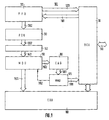
- a microprocessor 100 includes a bus control unit (BCU), 110 which initiates a bus cycle onto a system bus 190 interconnected with a memory and peripheral I/O units (not shown) and fetches instructions and reads and writes operand data.
- An instruction prefetch unit (PFU) 120 includes a prefetch address pointer (not shown) and issues an instruction prefetch request including the content of this pointer to BCU 110 through a bus 1201.
- the prefetched instructions from BCU 110 are transferred via an instruction bus 1101 to PFU 120 and temporarily stored therein.
- PFU 120 aligns the OP-code and the operand(s) of the prefetched instruction and outputs them onto a bus 1202.
- the information on the bus 1202 is supplied to a predecoder unit (PDU) 130 provided in accordance with the present invention.
- PDU 130 predecodes the OP-code and generates OP-code information indicative of the byte length of the OP-code and the number of operands to be processed.
- PDU 130 predecodes the operand(s) and generates addressing mode information indicative of the byte length of the operand and a designated addressing mode.
- the OP-code information and the addressing mode information are transferred onto a bus 1302 and temporarily stored in a buffer (BFF) 140 together with other information on the bus 1202.
- BFF 140 main decoder unit
- MDU main decoder unit
- MDU 150 determines decoding sequence in response to the OP-code information and the addressing mode information and performed a decoding operation in accordance with the determined decoding sequence to generate operand access information 1502 for accessing the operand and data processing information 1501 for executing the required instruction.
- the operand access information 1502 is supplied to an effective address generator unit (EAG) 160 which calculates and produces an effective address 1601 of the operand data.
- EAG effective address generator unit
- the effective address 1601 is supplied to a memory management unit (MMU) 170 and then translated into a read address.
- MMU 170 informs MDU 150 of the completion of the address translation through a signal 1702.
- MMU 170 further issues an operand access request to BCU 110 by supplying the real address.
- the data processing information 1501 from MDU 150 is supplied to an execution control unit (EXU) 180 which thus executes the required instruction or data process with receiving or transferring operand data from or to BCU 110 via a bus 1801.
- EXU execution control unit
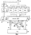
- FIG. 2 there are shown internal block constructions of PFU 120, PDU 130, BFF 140 and MDU 150. If should be noted that there are shown only parts related to the present invention in order to avoid the complication of the drawing.
- the instruction bus 1101 from BCU 110 has a 32-bit length (i.e., a 4-byte length), and hence the instruction data having four bytes is prefetched by one prefetch operation and then transferred onto the bus 1101.
- the bus 1101 is connected in common to four pockets (INSQ0 to INSQ3) 121-1 to 121-4 of an instruction queue 121, each of which has a 4-byte memory capacity.
- the instruction data of 4-byte from the bus 1101 is thus stored temporarily into one of the instruction queue pockets INSQ0-3 designated by queue pointer information 1241 generated by a queue controller 124.
- the queue pockets INSQ0-3 are designated in that order. For example, when the first queue pocket INSQ0 stores unprocessed instruction data, the instruction data on the bus 1101 is stored into the second queue pocket INSQ1.
- the contents of the queue pockets INSQ0-3 are tied up into instruction data 122 of a 16-byte length and then supplied to an instruction aligner 123.
- This aligner 123 includes an OP-code field output bus 126 of a 2-byte length, an addressing field output bus 127 of a 2-byte length and a data output bus 128 of a 4-byte length.
- the total byte length of one instruction including an OP-code field and an operand field is not constant, but is changed within a range from few bytes to ten and several bytes in dependence on the required data processing operation and/or the addressing mode of the operand(s). Therefore, the instruction aligner 123 responds to aligning pointer information 1251 from a aligner controller 125 and aligns the instruction data on the bus 122 such that the OP-code field, the addressing field and the displacement or immediate data of an instruction to be executed are transferred onto the buses 126, 127 and 128, respectively. These buses 126 to 128 correspond to the bus 1202 shown in Fig. 1.
- the OP-code data on the bus 126 and the addressing field data on the bus 127 are supplied to an OP-code field (OPF) predecoder 131 and an addressing field (AF) predecoder 132 of PDU 130, respectively.
- OPF predecoder 131 produces OP-code information 133 representative of the byte length of the OP-code field and the number of operands to be processed.
- AF predecoder 132 produces addressing mode information 134 representative of the byte length of the operand and the addressing mode designated thereto in response to the addressing field.
- These sets of information 133 and 134 are supplied to the aligner controller 125 and the queue controller 124 of PFU 120.
- the aligner controller 125 In response to the sets of information 133 and 134, the aligner controller 125 generates the aligning pointer information 1251 for controlling the positions and the number of the byte data to be outputted by the instruction aligner 123, and the queue controller 124 generates the queue pointer information 1241 for controlling the queue pocket INSQ into which the instruction data are stored from the bus 1101.
- the OP-code information 133 and the addressing mode information 134 are temporarily stored into buffer registers (BFFR1 and BFFR3) 141 and 143, respectively.
- the OP-code field and the addressing field outputted from the aligner 123 are further transferred to BFF 140 via branch buses 1261 and 1271 and then temporarily stored in BFFR2 and BFFR4, respectively.
- the displacement data or the immediate data from the aligner 123 is supplied via the bus 128 to BFF 140 and then temporarily stored in BFFR5 thereof.
- the buses for information 133 and 134, the branch buses 1261 and 1271 and the bus 128 correspond to the bus 1302 shown in Fig. 1.
- the controller 151 determines immediately the decoding sequence to be performed since the information 133 and 134 has the above-mentioned contents, and then produces the determined sequence information 1511 and 1512.
- the sequence information 1511 is supplied to an OPF main decoder 152 which also receives the OP-code field data from BFFR2. Accordingly, the decoder 152 generates data processing information 1501 necessary for instruction execution and supplies it to EXU 180.
- the addressing field data from BFFR4 is supplied to an AF main decoder 153 and the displacement or immediate data from BFFR5 is supplied to an operand access information generator 154.
- These units 153 and 154 operates in accordance with the addressing sequence information 1512 and thus generates the operand access information 1502 which is in turn supplied to EAG 160.
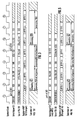
- Figs. 6A and 6B Two examples representative of different instruction formats are shown in Figs. 6A and 6B.
- the instruction shown in Fig. 6A is a 2-operand instruction 500 having a first operand to which a displacement mode is designated as an addressing mode and a second operand to which a displacement indexed mode is designated as an addressing mode.
- this instruction 500 is composed of the OP-code field 501 of 2-byte length, a first operand addressing mode (OPND1-AM) field 502 of 1-byte length, displacement data 503 of 4-byte length, a second operand (OPND2) index field 504 of 1-byte length, an AM mode field 505 of 1-byte length and displacement data 506 of 2-byte length, and thus has 11-byte length in total.
- the instruction shown in Figs. 6B is a 1-operand instruction 550 in which a displacement indexed mode is designated as addressing mode for one operand.
- This instruction 550 is composed of an OP-code field 510 of 1-byte length, an index field 511 of 1-byte length, an AM field 512 of 1-byte length and displacement data of 4-byte length, and thus has 7-byte length in total.
- the aligner controller 125 controls the aligning pointer information 1251 such that the instruction aligner 123 outputs the first and second byte data of 16-byte instruction data 122 onto the bus 126 and the third and fourth byte data thereof onto the bus 127. That is, the OP-code field 501 of the instruction 500 is outputted onto the bus 126 and OPND1-AM field 502 and the first byte of the displacement data 503 are outputted onto the bus 127 during a first clock 1 of a system clock shown in Fig. 3. In response thereto, OPF predecoder 131 produces the OP-code information 133 and AF predecoder 132 produces the addressing mode information 134.
- the OP-code information 133 represents that the instruction 500 has an OP-code field of 2-byte length and two operands.
- the addressing mode information 134 represents that the first operand has a displacement mode addressing and the displacement data has 4-byte length. It is noted that the first byte of the displacement 503 supplied to AF predecoder 132 is ignored.
- the aligner controller 125 controls the content of the pointer information 1251 such that the instruction aligner 123 outputs the fourth to seventh byte of the 16-byte instruction data 122 onto the bus 128 during the next clock 2, and the queue controller 124 controls the contents of the pointer information 1241 such that new instruction data are allowed to be stored into the first to third byte positions of the queue pocket INSQ0.
- the instruction aligner 123 In response to the beginning of the clock 2, the information 133 and 134 and the field data 501 and 502 from PDU 130 are stored into the corresponding buffer registers BFFR of BFF 140.
- the instruction aligner 123 outputs the displacement data 503 of 4-byte length onto the bus 128.
- MDU 150 performs the decoding operation in accordance with the decoding sequence information determined by the sequence controller 151.
- OPF main decoder 152 produces the data processing information 1501 representative of the required operation on two operand data
- AF main decoder 153 advances the access information generating operation to a state in which only the displacement 503 is required to complete the generation of the operand access information 1502.
- the aligner controller 125 controls the content of the pointer information 1251 such that the instruction aligner 123 outputs the ninth and tenth byte of the instruction data 122 onto the bus 127 during a next clock 3.
- the displacement data 503 is stored in BFFR5, so that MDU 150 completes the generation of the operand access information 1502 for the first operand data, the information 1502 being in turn transferred to EAG 160.
- OPND2 index field data 504 and AM field data 505 are outputted onto the bus 127 from the aligner 123. Therefore, AF predecoder 132 produces the addressing mode information 134 representing that the addressing mode of the second operand is a displacement indexed mode and the displacement data has 2-byte length.
- MDU 150 starts to generate the access information for the second operand data, and the instruction aligner 123 outputs the displacement data 506 onto the bus 128.
- the displacement data 506 is supplied to MDU 150 via BFFR5, and hence the operand access information 1502 for the second operand data is generated and supplied to EAG 160.
- the aligner controller 125 controls the pointer information 1251 to cause the instruction aligner 123 to output the twelfth and thirteenth byte data of the instruction data 122 onto the bus 126 and the fourteenth and fifteenth byte data thereof onto the bus 127, respectively, during the clock 5.
- the OP-code field 510 and the index field 511 of the instruction 510 are supplied to the OPF predecoder 131 and the AM field 512 and the first byte of the displacement 513 are supplied to AF predecoder 132.
- the information 133 from OPF predecoder 131 represents that the OP-code field has 1-byte length and the number of operand data is one.
- the aligner controller 125 detects that the index field 511 is not supplied to AF predecoder 132, and thus controls the pointer information 1251 to cause the instruction aligner 123 to output the fields 511 and 512 onto the bus 127 in a next clock 6.
- the OPF main decoder 152 performs the decoding operation during the clock 6, so that the data processing information 1501 for the instruction 550 is generated.
- the addressing mode information 134 from AF predecoder 132 and field data 511 and 512 are supplied to MDU 150.
- the information 134 represents that the displacement data 513 has 4-byte length.
- the instruction prefetch operation by PFU 120 has been performed during clocks 3 to 6, so that the remaining two byte data of the displacement 513 has been already stored in the first and second byte positions of the queue pocket INSQ0. Accordingly, all the four byte data of the displacement 513 are outputted from the aligner 123 during the clock 7, so that the operand access information for the operand data of the instruction 550 is generated in a next clock 8.
- PDU 140 releases MDU 150 from decoding of the instruction format and the operand addressing mode and from the control of the aligner 123.
- PDU 140 and MDU 150 operate in a pipelined manner by providing BFF 140 therebetween. Accordingly, the operation by PDU 140 can be put out of sight in a whole decoding operation. A high speed decoding operation is thus performed.
- the field data 511 and 512 of the instruction 550 are outputted twice from the instruction aligner 123, as described in the operation concerning clocks 5 and 6. If such a construction is realized that the decoding operation of the instruction 505 is completed by outputting the field data 511 and 512 from the aligner 123 only once, the decoding speed is further enhanced.
- the construction for this purpose is shown in Fig. 4 as another embodiment of the present invention, in which the same constituents as those shown in Fig. 2 are denoted by the same reference numerals to omit the further description thereof.
- the first 3 bits of the OP-code of the instruction having 1-byte length OP-code are all "1".
- a pattern detector 400 is provided to be connected to the instruction bus 1101. This detector 400 detects whether or not the first 3 bits of the respective byte data are all "1". When the first 3 bits are all "1", the detector 400 sets the corresponding bit of a flag register 401 to "1". On the other hand, in case where at least one of the 3 bits is "0", the detector 400 resets the corresponding bit of the register 401 to "0".
- the flag register 401 is thus of a 16-bit construction.
- the content of the register 401 is supplied to a flag aligner 402 which also receives the pointer information 1251.
- the aligner 402 selects one bit of the register 401 and outputs the selected bit data.
- the flag aligner 402 outputs the data of one bit of the register 401 which bit corresponds the position of the byte data of the 16-byte data 122 outputted onto the first byte bus 126-7 of the bus 126 by the instruction aligner 123.
- the flag aligner 402 outputs the twelfth bit data of the flag register 401.
- the second byte bus 126-2 of the bus 126 and the first byte bus 127-1 of the bus 127 are coupled to a multiplexer (MPX) 404, and the first and second byte buses 127-1 and 127-2 of the bus 127 are coupled to a multiplexer (MPX) 405.
- MPXs 404 and 405 are tied us as the addressing field output bus 127 coupled to PDU 130.
- MPXs 404 and 405 are controlled by the data 403 from the flag aligner 402. When this data 403 takes "1", MPXs 404 and 405 select the buses 126-2 and 127-1, respectively. When the data 403 is "0", the buses 127-1 and 127-2 are selected by MPXs 404 and 405, respectively.
- FIG. 5 An operation timing chart according to this embodiment is shown in Fig. 5 in comparison with that shown in Fig. 3 according to the previous embodiment.
- the flag aligner 402 When the OP-code field data 501 of the instruction 500 is outputted onto the bus 126 at the clock 1, the flag aligner 402 outputs the data 403 of "0", since the OP-code field 501 has 2-byte length. Accordingly, outputted onto the bus 127 are AM field data 502 and the first byte of the displacement data 503. Thus, the aligning operation and the decoding operation with respect to the instruction 500 are identical in both embodiments.
- the flag aligner 402 when the OP-code field data 510 of the instruction 550 is outputted onto the bus 126-1 at the clock 5, the flag aligner 402 outputs the data 403 of "1".
- the index field data 511 on the bus 126-2 is transferred as a first byte data onto the bus 127 via MPX 404, and the AM field data 512 on the bus 127-1 is transferred as a second byte data onto the bus 127 via MPX 405.
- These field data 511 and 512 are thereby supplied to AF predecoder 132.
- the displacement data 513 is outputted from the aligner 123 at the clock 6, and the decoding operation for the instruction 550 is completed at the clock 7.
- the decoding speed is further enhanced.
Description
- The present invention relates to a microprocessor and, more particularly, to an improvement in instruction decoder unit of a pipelined microprocessor.
- A pipelined microprocessor is constructed basically of six units: a bus control unit (BCU) for initiating a bus cycle to perform an instruction fetch operation and operand data read/write operation, an instruction prefetch unit (PFU) for requesting an instruction fetch bus cycle to BCU to prefetch instructions, an instruction decoder unit (IDU) for decoding the instruction from PFU and generating data processing information necessary for instruction execution and operand access information necessary for an operand data access, an effective address generator unit (EAG) for calculating an effective address in response to the operand access information, a memory management unit (MMU) for translating the effective address into a real address and requesting an operand data access to BCU, and an instruction execurtion unit (EXU) for executing an instruction in response to the data processing information from IDU. These units operate in parallel in a predetermined pipeline processing manner.
- In a recent year, a microprocess has been required to facilitate software programming. For this purpose, an abundance of instruction formats are prepared, and moreover it is supported that an independent addressing mode can be designated to respective operands. Also in the addressing mode, there are prepared a plenty of addressing modes such as direct/indirect modes, displacement modes, indexed modes and so forth.
- However, the support of abundant instruction formats and addressing modes causes an instruction decoding time being prolonged. Specifically, IDU decodes an instruction to be executed and generates the data processing information and the operand access information in accordance with the decoding sequence determined by the format and the operand addressing mode of that instruction. Therefore, the support of many instruction formats and operand addressing modes prolongs a time for decoding and detecting the format and the operand addressing mode of an instruction to be executed to determine the decoding sequence. The generation of the data processing information and the operand access information is thereby delayed to disturb the pipeline processing operation. The execution efficiency of the microprocessor is thus lowered.
- A microprocessor characterized in that an instruction decoding operation is performed by a predecoder unit and a main decoder unit which cperate in a pipeline manner by providing between those two units a buffer for temporarily storing information from the predecoder unit is disclosed in EP-A-0 336 091 (Art.54(3)).
- An object of the present invention is to provide a microprocessor supporting abundant instruction formats and operand addressing modes without lowering an instruction decoding speed.
- This object is attained by the microprocessor defined in the appended claim.
- The predecoder unit of the claimed microprocessor includes first and second predecoder respectively receiving an operation code (called hereinafter "OP-code") field and an addressing field of an instruction to be executed. The first predecoder predecodes the OP-code field and produces OP-code information representative of the number of bytes of the OP-code field and the number of operands to be processed. The second predecoder predecodes the addressing field and produces addressing mode information representative of the number of bytes of the operand and the addressing mode designated to the operand. The OP-code information and the addressing mode information are temporarily stored in the buffer. The buffer also stores the OP-code and addressing fields of the instruction, and further stores displacement data and immediate data of the instruction. The main decoder unit determines the decoding sequence to be preformed in response to the OP-code information and the addressing mode information from the buffer, and performs the decoding operation on other information from the buffer to generate data processing information and operand access information in accordance with the determined decoding sequence. During the decoding operation of the main decoder unit, the predecoder unit is performing the predecoding operation on a second operand or an instruction to be next executed.
- That is, the present invention is based upon the finding that the decoding operation on an instruction consists in general of a first operation of detecting the format and the operand addressing mode of the instruction and a second operation of generating decoded instruction information in response to the decoding sequence determined by the detected result in the first step, and thus allots the first and second steps respectively to the predecoder unit and the main decoder unit which operate in a pipelined manner. Accordingly, the first operation is performed in parallel with the second operation, so that the operation time of the predecoder unit is put out of sight by the operation time of the main decoder unit. The whole pipeline processing operation of the microprocessor is thus hardly disturbed to enhance the program execution efficiency thereof.
- The above and other object, advantages and features of the present invention will be more apparent from the following description taken in conjunction with the accompanying drawings, in which:
- Fig. 1 is a block diagram representative of an embodiment of the present invention;
- Fig. 2 is a block diagram representative of constructions of PFU, PDU, BFF and MDU shown in Fig. 1;
- Fig. 3 is a timing chart for explaining an operation of the circuit shown in Fig. 2;
- Fig. 4 is a block diagram representative of PFU according to another embodiment of the present invention;
- Fig. 5 is a timing chart for explaining an operation of the circuit shown in Fig. 4; and
- Figs. 6A and 6B are format diagrams indicative of two examples of instructions.
- Referring now to Fig. 1, a
microprocessor 100 according to an embodiment of the present invention includes a bus control unit (BCU), 110 which initiates a bus cycle onto asystem bus 190 interconnected with a memory and peripheral I/O units (not shown) and fetches instructions and reads and writes operand data. An instruction prefetch unit (PFU) 120 includes a prefetch address pointer (not shown) and issues an instruction prefetch request including the content of this pointer to BCU 110 through abus 1201. The prefetched instructions from BCU 110 are transferred via aninstruction bus 1101 to PFU 120 and temporarily stored therein. PFU 120 aligns the OP-code and the operand(s) of the prefetched instruction and outputs them onto abus 1202. The information on thebus 1202 is supplied to a predecoder unit (PDU) 130 provided in accordance with the present invention. PDU 130 predecodes the OP-code and generates OP-code information indicative of the byte length of the OP-code and the number of operands to be processed. Moreover, PDU 130 predecodes the operand(s) and generates addressing mode information indicative of the byte length of the operand and a designated addressing mode. The OP-code information and the addressing mode information are transferred onto abus 1302 and temporarily stored in a buffer (BFF) 140 together with other information on thebus 1202. The contents of BFF 140 are supplied to a main decoder unit (MDU) 150 via a bus 1401. MDU 150 determines decoding sequence in response to the OP-code information and the addressing mode information and performed a decoding operation in accordance with the determined decoding sequence to generateoperand access information 1502 for accessing the operand anddata processing information 1501 for executing the required instruction. Theoperand access information 1502 is supplied to an effective address generator unit (EAG) 160 which calculates and produces aneffective address 1601 of the operand data. Theeffective address 1601 is supplied to a memory management unit (MMU) 170 and then translated into a read address.MMU 170 informsMDU 150 of the completion of the address translation through asignal 1702. MMU 170 further issues an operand access request to BCU 110 by supplying the real address. Thedata processing information 1501 from MDU 150 is supplied to an execution control unit (EXU) 180 which thus executes the required instruction or data process with receiving or transferring operand data from or to BCU 110 via a bus 1801. These units, BCU 110, PFU 120, PDU 130, MDU 150, EAG 160, MMU 170 and EXU 180, operates in parallel in a pipelined manner. - Turning to Fig. 2, there are shown internal block constructions of
PFU 120, PDU 130, BFF 140 and MDU 150. If should be noted that there are shown only parts related to the present invention in order to avoid the complication of the drawing. Theinstruction bus 1101 from BCU 110 has a 32-bit length (i.e., a 4-byte length), and hence the instruction data having four bytes is prefetched by one prefetch operation and then transferred onto thebus 1101. Thebus 1101 is connected in common to four pockets (INSQ0 to INSQ3) 121-1 to 121-4 of aninstruction queue 121, each of which has a 4-byte memory capacity. The instruction data of 4-byte from thebus 1101 is thus stored temporarily into one of the instruction queue pockets INSQ0-3 designated byqueue pointer information 1241 generated by aqueue controller 124. The queue pockets INSQ0-3 are designated in that order. For example, when the first queue pocket INSQ0 stores unprocessed instruction data, the instruction data on thebus 1101 is stored into the second queue pocket INSQ1. The contents of the queue pockets INSQ0-3 are tied up intoinstruction data 122 of a 16-byte length and then supplied to aninstruction aligner 123. Thisaligner 123 includes an OP-codefield output bus 126 of a 2-byte length, an addressingfield output bus 127 of a 2-byte length and adata output bus 128 of a 4-byte length. The total byte length of one instruction including an OP-code field and an operand field is not constant, but is changed within a range from few bytes to ten and several bytes in dependence on the required data processing operation and/or the addressing mode of the operand(s). Therefore, the instruction aligner 123 responds to aligningpointer information 1251 from aaligner controller 125 and aligns the instruction data on thebus 122 such that the OP-code field, the addressing field and the displacement or immediate data of an instruction to be executed are transferred onto thebuses buses 126 to 128 correspond to thebus 1202 shown in Fig. 1. - The OP-code data on the
bus 126 and the addressing field data on thebus 127 are supplied to an OP-code field (OPF)predecoder 131 and an addressing field (AF)predecoder 132 ofPDU 130, respectively. In response to the OP-code field data,OPF predecoder 131 produces OP-code information 133 representative of the byte length of the OP-code field and the number of operands to be processed.AF predecoder 132 produces addressingmode information 134 representative of the byte length of the operand and the addressing mode designated thereto in response to the addressing field. These sets ofinformation 133 and 134 are supplied to thealigner controller 125 and thequeue controller 124 ofPFU 120. In response to the sets ofinformation 133 and 134, thealigner controller 125 generates the aligningpointer information 1251 for controlling the positions and the number of the byte data to be outputted by theinstruction aligner 123, and thequeue controller 124 generates thequeue pointer information 1241 for controlling the queue pocket INSQ into which the instruction data are stored from thebus 1101. The OP-code information 133 and the addressingmode information 134 are temporarily stored into buffer registers (BFFR1 and BFFR3) 141 and 143, respectively. The OP-code field and the addressing field outputted from thealigner 123 are further transferred toBFF 140 viabranch buses aligner 123 is supplied via thebus 128 toBFF 140 and then temporarily stored in BFFR5 thereof. The buses forinformation 133 and 134, thebranch buses bus 128 correspond to thebus 1302 shown in Fig. 1. - The data stored in BFFR1 and BFFR2, i.e. the CP-code information 133 and the addressing
mode information 134, are supplied to a decoding sequence controller 151 ofMDU 150. The controller 151 thus determines immediately the decoding sequence to be performed since theinformation 133 and 134 has the above-mentioned contents, and then produces thedetermined sequence information sequence information 1511 is supplied to an OPF main decoder 152 which also receives the OP-code field data from BFFR2. Accordingly, the decoder 152 generatesdata processing information 1501 necessary for instruction execution and supplies it toEXU 180. The addressing field data from BFFR4 is supplied to an AFmain decoder 153 and the displacement or immediate data from BFFR5 is supplied to an operandaccess information generator 154. Theseunits sequence information 1512 and thus generates theoperand access information 1502 which is in turn supplied toEAG 160. - As mentioned above, the whole byte length of an instruction to be executed changes in dependence on the required data processing operation and the addressing mode designated to the operand(s) to be processed. Two examples representative of different instruction formats are shown in Figs. 6A and 6B. The instruction shown in Fig. 6A is a 2-
operand instruction 500 having a first operand to which a displacement mode is designated as an addressing mode and a second operand to which a displacement indexed mode is designated as an addressing mode. In detail, thisinstruction 500 is composed of the OP-code field 501 of 2-byte length, a first operand addressing mode (OPND1-AM)field 502 of 1-byte length,displacement data 503 of 4-byte length, a second operand (OPND2)index field 504 of 1-byte length, anAM mode field 505 of 1-byte length anddisplacement data 506 of 2-byte length, and thus has 11-byte length in total. The instruction shown in Figs. 6B is a 1-operand instruction 550 in which a displacement indexed mode is designated as addressing mode for one operand. Thisinstruction 550 is composed of an OP-code field 510 of 1-byte length, an index field 511 of 1-byte length, an AM field 512 of 1-byte length and displacement data of 4-byte length, and thus has 7-byte length in total. - Next, an operation will be made below with reference to Figs. 1, 2 and 6 and further to Fig. 3 showing a timing chart. Assume that the
instructions instruction queue 121. However, since theinstruction queue 121 is of 16-byte length in total, the lower order two-type data of thedisplacement 513 of theinstruction 550 is not yet stored in thequeue 121. - Since the previous instruction has been already transferred
PDU 130, thealigner controller 125 controls the aligningpointer information 1251 such that theinstruction aligner 123 outputs the first and second byte data of 16-byte instruction data 122 onto thebus 126 and the third and fourth byte data thereof onto thebus 127. That is, the OP-code field 501 of theinstruction 500 is outputted onto thebus 126 and OPND1-AM field 502 and the first byte of thedisplacement data 503 are outputted onto thebus 127 during afirst clock ① of a system clock shown in Fig. 3. In response thereto,OPF predecoder 131 produces the OP-code information 133 andAF predecoder 132 produces the addressingmode information 134. The OP-code information 133 represents that theinstruction 500 has an OP-code field of 2-byte length and two operands. The addressingmode information 134 represents that the first operand has a displacement mode addressing and the displacement data has 4-byte length. It is noted that the first byte of thedisplacement 503 supplied to AF predecoder 132 is ignored. In response to those contents of theinformation 133 and 134, thealigner controller 125 controls the content of thepointer information 1251 such that theinstruction aligner 123 outputs the fourth to seventh byte of the 16-byte instruction data 122 onto thebus 128 during thenext clock ②, and thequeue controller 124 controls the contents of thepointer information 1241 such that new instruction data are allowed to be stored into the first to third byte positions of the queue pocket INSQ0. - In response to the beginning of the
clock ②, theinformation 133 and 134 and thefield data PDU 130 are stored into the corresponding buffer registers BFFR ofBFF 140. On the other hand, theinstruction aligner 123 outputs thedisplacement data 503 of 4-byte length onto thebus 128. During thisclock ②,MDU 150 performs the decoding operation in accordance with the decoding sequence information determined by the sequence controller 151. Thus, OPF main decoder 152 produces thedata processing information 1501 representative of the required operation on two operand data, and AFmain decoder 153 advances the access information generating operation to a state in which only thedisplacement 503 is required to complete the generation of theoperand access information 1502. Thealigner controller 125 controls the content of thepointer information 1251 such that theinstruction aligner 123 outputs the ninth and tenth byte of theinstruction data 122 onto thebus 127 during anext clock ③. - When the
clock ③ appears, thedisplacement data 503 is stored in BFFR5, so thatMDU 150 completes the generation of theoperand access information 1502 for the first operand data, theinformation 1502 being in turn transferred toEAG 160. On the other hand, OPND2index field data 504 andAM field data 505 are outputted onto thebus 127 from thealigner 123. Therefore,AF predecoder 132 produces the addressingmode information 134 representing that the addressing mode of the second operand is a displacement indexed mode and the displacement data has 2-byte length. - In a
clock ④,MDU 150 starts to generate the access information for the second operand data, and theinstruction aligner 123 outputs thedisplacement data 506 onto thebus 128. During anext clock ⑤, thedisplacement data 506 is supplied toMDU 150 via BFFR5, and hence theoperand access information 1502 for the second operand data is generated and supplied toEAG 160. When theinstruction aligner 123 outputs thedisplacement data 506, the aligning operation for theinstruction 500 is completed. Therefore, thealigner controller 125 controls thepointer information 1251 to cause theinstruction aligner 123 to output the twelfth and thirteenth byte data of theinstruction data 122 onto thebus 126 and the fourteenth and fifteenth byte data thereof onto thebus 127, respectively, during theclock ⑤. Thus, the OP-code field 510 and the index field 511 of the instruction 510 are supplied to the OPF predecoder 131 and the AM field 512 and the first byte of thedisplacement 513 are supplied toAF predecoder 132. The information 133 from OPF predecoder 131 represents that the OP-code field has 1-byte length and the number of operand data is one. Accordingly, thealigner controller 125 detects that the index field 511 is not supplied toAF predecoder 132, and thus controls thepointer information 1251 to cause theinstruction aligner 123 to output the fields 511 and 512 onto thebus 127 in anext clock ⑥. On the other hand, the OPF main decoder 152 performs the decoding operation during theclock ⑥, so that thedata processing information 1501 for theinstruction 550 is generated. - When a next clock ⑦ appears, the addressing
mode information 134 from AF predecoder 132 and field data 511 and 512 are supplied toMDU 150. Theinformation 134 represents that thedisplacement data 513 has 4-byte length. In addition, the instruction prefetch operation byPFU 120 has been performed duringclocks ③ to ⑥, so that the remaining two byte data of thedisplacement 513 has been already stored in the first and second byte positions of the queue pocket INSQ0. Accordingly, all the four byte data of thedisplacement 513 are outputted from thealigner 123 during the clock ⑦, so that the operand access information for the operand data of theinstruction 550 is generated in anext clock ⑧. - Thus, although the decoding sequence and the control to the
instruction aligner 123 are changed in dependence on the format and the operand addressing mode of an instruction to be executed,PDU 140releases MDU 150 from decoding of the instruction format and the operand addressing mode and from the control of thealigner 123. Moreover,PDU 140 andMDU 150 operate in a pipelined manner by providingBFF 140 therebetween. Accordingly, the operation byPDU 140 can be put out of sight in a whole decoding operation. A high speed decoding operation is thus performed. - In the above embodiment, the field data 511 and 512 of the
instruction 550 are outputted twice from theinstruction aligner 123, as described in theoperation concerning clocks instruction 505 is completed by outputting the field data 511 and 512 from thealigner 123 only once, the decoding speed is further enhanced. The construction for this purpose is shown in Fig. 4 as another embodiment of the present invention, in which the same constituents as those shown in Fig. 2 are denoted by the same reference numerals to omit the further description thereof. - In this embodiment, it is utilized that the first 3 bits of the OP-code of the instruction having 1-byte length OP-code are all "1". Specifically, a
pattern detector 400 is provided to be connected to theinstruction bus 1101. Thisdetector 400 detects whether or not the first 3 bits of the respective byte data are all "1". When the first 3 bits are all "1", thedetector 400 sets the corresponding bit of a flag register 401 to "1". On the other hand, in case where at least one of the 3 bits is "0", thedetector 400 resets the corresponding bit of the register 401 to "0". The flag register 401 is thus of a 16-bit construction. The content of the register 401 is supplied to aflag aligner 402 which also receives thepointer information 1251. In response to the content of thepointer information 1251, thealigner 402 selects one bit of the register 401 and outputs the selected bit data. In other words, theflag aligner 402 outputs the data of one bit of the register 401 which bit corresponds the position of the byte data of the 16-byte data 122 outputted onto the first byte bus 126-7 of thebus 126 by theinstruction aligner 123. For example, when theinstruction aligner 123 outputs the twelfth byte data of theinstruction data 122 onto the bus 126-1, theflag aligner 402 outputs the twelfth bit data of the flag register 401. The second byte bus 126-2 of thebus 126 and the first byte bus 127-1 of thebus 127 are coupled to a multiplexer (MPX) 404, and the first and second byte buses 127-1 and 127-2 of thebus 127 are coupled to a multiplexer (MPX) 405. The outputs fromMPXs field output bus 127 coupled toPDU 130.MPXs data 403 from theflag aligner 402. When thisdata 403 takes "1",MPXs data 403 is "0", the buses 127-1 and 127-2 are selected byMPXs - An operation timing chart according to this embodiment is shown in Fig. 5 in comparison with that shown in Fig. 3 according to the previous embodiment. When the OP-
code field data 501 of theinstruction 500 is outputted onto thebus 126 at theclock ①, theflag aligner 402 outputs thedata 403 of "0", since the OP-code field 501 has 2-byte length. Accordingly, outputted onto thebus 127 areAM field data 502 and the first byte of thedisplacement data 503. Thus, the aligning operation and the decoding operation with respect to theinstruction 500 are identical in both embodiments. On the other hand, when the OP-code field data 510 of theinstruction 550 is outputted onto the bus 126-1 at theclock ⑤, theflag aligner 402 outputs thedata 403 of "1". Accordingly, the index field data 511 on the bus 126-2 is transferred as a first byte data onto thebus 127 viaMPX 404, and the AM field data 512 on the bus 127-1 is transferred as a second byte data onto thebus 127 viaMPX 405. These field data 511 and 512 are thereby supplied toAF predecoder 132. As a result, thedisplacement data 513 is outputted from thealigner 123 at theclock ⑥, and the decoding operation for theinstruction 550 is completed at the clock ⑦. Thus, the decoding speed is further enhanced.
Claims (1)
- A microprocessor (100) having an instruction decoder unit which decodes an instruction to be executed and generates data processing information for executing said instruction and operand access information for accessing operand data of said instruction, said instruction decoder unit comprising a predecoder unit (130) receiving data of an operation code field and an addressing mode field of said instruction and generating operation code information relative to a format of said instruction and addressing mode information relative to an addressing mode designated to operand data to be processed, buffer means (140) coupled to receive in parallel said operation code information and said addressing mode information for temporarily storing and outputting in parallel said operation code information and said addresing mode information, a main decoder unit (150) receiving in parallel information outputted in parallel from said buffer means and generating said processing information and said operand access information in response thereto, said predecoder unit and said main decoder operating in a pipelined manner, an instruction aligner (123), said instruction aligner having an input bus (122) receiving said instruction and further having first, second and third output buses (126, 127, 128), said instruction further including a constant field, said instruction aligner (123) aligning said instruction to output the data of said operation code field, the data of said addressing mode field and the data of said constant field of said instruction onto said first, second and third buses, respectively, said precoder unit including first and second decoders (131, 132), said first decoder (131) coupled to said first bus (126) for decoding the data of said operation code field to produce said operation code information (133) that represents at least the byte length of said operation code field and the number of operands to be processed, said second decoder (132) coupled to said second bus for decoding the data of said addressing mode field to produce said addressing mode information (154) that represents at least the byte length of the operand and the addressing mode designated to said operand, said buffer being coupled to said third bus to store the data of said constant field, being supplied to an aligner controller (125) controlling said instruction aligner (123) for aligning the instruction data on said input bus (122) such that said operation code field, said addressing field and said displacement or immediate data of said instruction are transferred on said first, second and third output busses (126, 127, 128) respectively.
Applications Claiming Priority (2)
| Application Number | Priority Date | Filing Date | Title |
|---|---|---|---|
| JP222057/89 | 1989-08-28 | ||
| JP22205789 | 1989-08-28 |
Publications (3)
| Publication Number | Publication Date |
|---|---|
| EP0415366A2 EP0415366A2 (en) | 1991-03-06 |
| EP0415366A3 EP0415366A3 (en) | 1992-03-11 |
| EP0415366B1 true EP0415366B1 (en) | 1997-06-11 |
Family
ID=16776428
Family Applications (1)
| Application Number | Title | Priority Date | Filing Date |
|---|---|---|---|
| EP90116506A Expired - Lifetime EP0415366B1 (en) | 1989-08-28 | 1990-08-28 | Microprocessor having predecoder unit and main decoder unit operating in pipeline processing manner |
Country Status (5)
| Country | Link |
|---|---|
| US (1) | US5233696A (en) |
| EP (1) | EP0415366B1 (en) |
| JP (1) | JP2725450B2 (en) |
| KR (1) | KR940003383B1 (en) |
| DE (1) | DE69030905T2 (en) |
Families Citing this family (55)
| Publication number | Priority date | Publication date | Assignee | Title |
|---|---|---|---|---|
| JPH04156613A (en) * | 1990-10-20 | 1992-05-29 | Fujitsu Ltd | Instruction buffer device |
| EP0498654B1 (en) * | 1991-02-08 | 2000-05-10 | Fujitsu Limited | Cache memory processing instruction data and data processor including the same |
| US5452423A (en) * | 1991-06-13 | 1995-09-19 | Chips And Technologies, Inc. | Two-ROM multibyte microcode address selection method and apparatus |
| EP0650612B1 (en) * | 1992-03-25 | 1999-08-18 | Zilog Incorporated | Fast instruction decoding in a pipeline processor |
| US5371864A (en) * | 1992-04-09 | 1994-12-06 | International Business Machines Corporation | Apparatus for concurrent multiple instruction decode in variable length instruction set computer |
| US5542058A (en) * | 1992-07-06 | 1996-07-30 | Digital Equipment Corporation | Pipelined computer with operand context queue to simplify context-dependent execution flow |
| US5859994A (en) * | 1992-08-10 | 1999-01-12 | Intel Corporation | Apparatus and method for modifying instruction length decoding in a computer processor |
| US5603037A (en) * | 1993-04-23 | 1997-02-11 | Intel Corporation | Clock disable circuit for translation buffer |
| US5689672A (en) * | 1993-10-29 | 1997-11-18 | Advanced Micro Devices, Inc. | Pre-decoded instruction cache and method therefor particularly suitable for variable byte-length instructions |
| US5630082A (en) * | 1993-10-29 | 1997-05-13 | Advanced Micro Devices, Inc. | Apparatus and method for instruction queue scanning |
| DE69434669T2 (en) * | 1993-10-29 | 2006-10-12 | Advanced Micro Devices, Inc., Sunnyvale | Speculative command queue for variable byte length commands |
| US5878245A (en) * | 1993-10-29 | 1999-03-02 | Advanced Micro Devices, Inc. | High performance load/store functional unit and data cache |
| DE69427265T2 (en) * | 1993-10-29 | 2002-05-02 | Advanced Micro Devices Inc | Superskalarbefehlsdekoder |
| DE69427734T2 (en) | 1993-10-29 | 2002-05-23 | Advanced Micro Devices Inc | Linearly addressed microprocessor cache |
| US6360313B1 (en) | 1993-11-05 | 2002-03-19 | Intergraph Corporation | Instruction cache associative crossbar switch |
| DE69422780T2 (en) * | 1993-11-05 | 2000-08-17 | Intergraph Corp | Superscalar computer architecture with software scheduling |
| EP0652509B1 (en) * | 1993-11-05 | 2000-05-10 | Intergraph Corporation | Instruction cache associative cross-bar switch |
| US5974534A (en) * | 1994-02-14 | 1999-10-26 | Hewlett-Packard Company | Predecoding and steering mechanism for instructions in a superscalar processor |
| US5673427A (en) * | 1994-03-01 | 1997-09-30 | Intel Corporation | Packing valid micro operations received from a parallel decoder into adjacent locations of an output queue |
| US5608885A (en) * | 1994-03-01 | 1997-03-04 | Intel Corporation | Method for handling instructions from a branch prior to instruction decoding in a computer which executes variable-length instructions |
| JP2982618B2 (en) * | 1994-06-28 | 1999-11-29 | 日本電気株式会社 | Memory selection circuit |
| US5737550A (en) * | 1995-03-28 | 1998-04-07 | Advanced Micro Devices, Inc. | Cache memory to processor bus interface and method thereof |
| US5822558A (en) * | 1995-04-12 | 1998-10-13 | Advanced Micro Devices, Inc. | Method and apparatus for predecoding variable byte-length instructions within a superscalar microprocessor |
| US5991869A (en) * | 1995-04-12 | 1999-11-23 | Advanced Micro Devices, Inc. | Superscalar microprocessor including a high speed instruction alignment unit |
| US5859991A (en) * | 1995-06-07 | 1999-01-12 | Advanced Micro Devices, Inc. | Parallel and scalable method for identifying valid instructions and a superscalar microprocessor including an instruction scanning unit employing the method |
| US5926642A (en) | 1995-10-06 | 1999-07-20 | Advanced Micro Devices, Inc. | RISC86 instruction set |
| US5809273A (en) * | 1996-01-26 | 1998-09-15 | Advanced Micro Devices, Inc. | Instruction predecode and multiple instruction decode |
| US6093213A (en) * | 1995-10-06 | 2000-07-25 | Advanced Micro Devices, Inc. | Flexible implementation of a system management mode (SMM) in a processor |
| US5819056A (en) * | 1995-10-06 | 1998-10-06 | Advanced Micro Devices, Inc. | Instruction buffer organization method and system |
| US5794063A (en) * | 1996-01-26 | 1998-08-11 | Advanced Micro Devices, Inc. | Instruction decoder including emulation using indirect specifiers |
| US5920713A (en) * | 1995-10-06 | 1999-07-06 | Advanced Micro Devices, Inc. | Instruction decoder including two-way emulation code branching |
| US5872947A (en) * | 1995-10-24 | 1999-02-16 | Advanced Micro Devices, Inc. | Instruction classification circuit configured to classify instructions into a plurality of instruction types prior to decoding said instructions |
| US5892936A (en) * | 1995-10-30 | 1999-04-06 | Advanced Micro Devices, Inc. | Speculative register file for storing speculative register states and removing dependencies between instructions utilizing the register |
| US5796974A (en) * | 1995-11-07 | 1998-08-18 | Advanced Micro Devices, Inc. | Microcode patching apparatus and method |
| US5822559A (en) * | 1996-01-02 | 1998-10-13 | Advanced Micro Devices, Inc. | Apparatus and method for aligning variable byte-length instructions to a plurality of issue positions |
| US5867680A (en) * | 1996-07-24 | 1999-02-02 | Advanced Micro Devices, Inc. | Microprocessor configured to simultaneously dispatch microcode and directly-decoded instructions |
| US6049863A (en) * | 1996-07-24 | 2000-04-11 | Advanced Micro Devices, Inc. | Predecoding technique for indicating locations of opcode bytes in variable byte-length instructions within a superscalar microprocessor |
| US5961632A (en) * | 1996-07-25 | 1999-10-05 | Texas Instruments Incorporated | Microprocessor with circuits, systems, and methods for selecting alternative pipeline instruction paths based on instruction leading codes |
| US5852727A (en) * | 1997-03-10 | 1998-12-22 | Advanced Micro Devices, Inc. | Instruction scanning unit for locating instructions via parallel scanning of start and end byte information |
| US5859992A (en) * | 1997-03-12 | 1999-01-12 | Advanced Micro Devices, Inc. | Instruction alignment using a dispatch list and a latch list |
| US5940602A (en) * | 1997-06-11 | 1999-08-17 | Advanced Micro Devices, Inc. | Method and apparatus for predecoding variable byte length instructions for scanning of a number of RISC operations |
| US6105125A (en) * | 1997-11-12 | 2000-08-15 | National Semiconductor Corporation | High speed, scalable microcode based instruction decoder for processors using split microROM access, dynamic generic microinstructions, and microcode with predecoded instruction information |
| US6134649A (en) * | 1997-11-17 | 2000-10-17 | Advanced Micro Devices, Inc. | Control transfer indication in predecode which identifies control transfer instruction and an alternate feature of an instruction |
| US6167506A (en) | 1997-11-17 | 2000-12-26 | Advanced Micro Devices, Inc. | Replacing displacement in control transfer instruction with encoding indicative of target address, including offset and target cache line location |
| EP0942357A3 (en) * | 1998-03-11 | 2000-03-22 | Matsushita Electric Industrial Co., Ltd. | Data processor compatible with a plurality of instruction formats |
| US6061786A (en) * | 1998-04-23 | 2000-05-09 | Advanced Micro Devices, Inc. | Processor configured to select a next fetch address by partially decoding a byte of a control transfer instruction |
| US6094716A (en) | 1998-07-14 | 2000-07-25 | Advanced Micro Devices, Inc. | Register renaming in which moves are accomplished by swapping rename tags |
| US6240503B1 (en) | 1998-11-12 | 2001-05-29 | Advanced Micro Devices, Inc. | Cumulative lookahead to eliminate chained dependencies |
| US6425069B1 (en) | 1999-03-05 | 2002-07-23 | International Business Machines Corporation | Optimization of instruction stream execution that includes a VLIW dispatch group |
| US6438664B1 (en) | 1999-10-27 | 2002-08-20 | Advanced Micro Devices, Inc. | Microcode patch device and method for patching microcode using match registers and patch routines |
| US6816962B2 (en) * | 2002-02-25 | 2004-11-09 | International Business Machines Corporation | Re-encoding illegal OP codes into a single illegal OP code to accommodate the extra bits associated with pre-decoded instructions |
| US7484075B2 (en) * | 2002-12-16 | 2009-01-27 | International Business Machines Corporation | Method and apparatus for providing fast remote register access in a clustered VLIW processor using partitioned register files |
| US7043626B1 (en) | 2003-10-01 | 2006-05-09 | Advanced Micro Devices, Inc. | Retaining flag value associated with dead result data in freed rename physical register with an indicator to select set-aside register instead for renaming |
| JP7004905B2 (en) * | 2018-03-26 | 2022-01-21 | 富士通株式会社 | Arithmetic processing unit and control method of arithmetic processing unit |
| KR102184099B1 (en) * | 2019-03-22 | 2020-11-27 | 노윤호 | Extra cooling system for preform |
Family Cites Families (8)
| Publication number | Priority date | Publication date | Assignee | Title |
|---|---|---|---|---|
| US4437149A (en) * | 1980-11-17 | 1984-03-13 | International Business Machines Corporation | Cache memory architecture with decoding |
| US4685080A (en) * | 1982-02-22 | 1987-08-04 | International Business Machines Corp. | Microword generation mechanism utilizing separate programmable logic arrays for first and second microwords |
| JPS60129837A (en) * | 1983-12-19 | 1985-07-11 | Matsushita Electric Ind Co Ltd | Signal processing operation processor |
| US4873629A (en) * | 1984-06-20 | 1989-10-10 | Convex Computer Corporation | Instruction processing unit for computer |
| JPS6391739A (en) * | 1986-10-06 | 1988-04-22 | Matsushita Electric Ind Co Ltd | Decoder for variable length instruction |
| JPH01255036A (en) * | 1988-04-04 | 1989-10-11 | Toshiba Corp | Microprocessor |
| US5101341A (en) * | 1988-08-25 | 1992-03-31 | Edgcore Technology, Inc. | Pipelined system for reducing instruction access time by accumulating predecoded instruction bits a FIFO |
| JPH0769824B2 (en) * | 1988-11-11 | 1995-07-31 | 株式会社日立製作所 | Multiple instruction simultaneous processing method |
-
1990
- 1990-08-28 US US07/573,746 patent/US5233696A/en not_active Expired - Fee Related
- 1990-08-28 EP EP90116506A patent/EP0415366B1/en not_active Expired - Lifetime
- 1990-08-28 DE DE69030905T patent/DE69030905T2/en not_active Expired - Fee Related
- 1990-08-28 KR KR1019900013277A patent/KR940003383B1/en not_active IP Right Cessation
- 1990-08-28 JP JP2226134A patent/JP2725450B2/en not_active Expired - Lifetime
Also Published As
| Publication number | Publication date |
|---|---|
| EP0415366A3 (en) | 1992-03-11 |
| DE69030905D1 (en) | 1997-07-17 |
| JP2725450B2 (en) | 1998-03-11 |
| JPH03156533A (en) | 1991-07-04 |
| US5233696A (en) | 1993-08-03 |
| KR910005156A (en) | 1991-03-30 |
| EP0415366A2 (en) | 1991-03-06 |
| DE69030905T2 (en) | 1998-01-29 |
| KR940003383B1 (en) | 1994-04-21 |
Similar Documents
| Publication | Publication Date | Title |
|---|---|---|
| EP0415366B1 (en) | Microprocessor having predecoder unit and main decoder unit operating in pipeline processing manner | |
| US4875160A (en) | Method for implementing synchronous pipeline exception recovery | |
| JP2679363B2 (en) | Microprocessor | |
| US5218711A (en) | Microprocessor having program counter registers for its coprocessors | |
| US4648034A (en) | Busy signal interface between master and slave processors in a computer system | |
| EP0239081B1 (en) | Pipelined data processor capable of decoding and executing plural instructions in parallel | |
| EP0689128B1 (en) | Computer instruction compression | |
| EP0138419B1 (en) | Central processing unit for a digital computer | |
| US6463520B1 (en) | Processor for executing instruction codes of two different lengths and device for inputting the instruction codes | |
| EP1359501A2 (en) | A processing device for executing virtual machine instructions | |
| US4897787A (en) | Data processing system | |
| US5249280A (en) | Microcomputer having a memory bank switching apparatus for accessing a selected memory bank in an external memory | |
| US5327536A (en) | Microprocessor having branch prediction function | |
| US5313644A (en) | System having status update controller for determining which one of parallel operation results of execution units is allowed to set conditions of shared processor status word | |
| US6338134B1 (en) | Method and system in a superscalar data processing system for the efficient processing of an instruction by moving only pointers to data | |
| EP0417013A2 (en) | Data processor decoding and executing a train of instructions of variable length | |
| US7366882B2 (en) | Address calculation unit for an object oriented processor having differentiation circuitry for selectively operating micro-instructions | |
| US20030028754A1 (en) | Data processor using indirect register addressing | |
| US11836494B2 (en) | System and method for addressing data in memory | |
| CA2003004C (en) | Apparatus and method for executing a conditional branch instruction | |
| EP0240606B1 (en) | Pipe-line processing system and microprocessor using the system | |
| JPH03233630A (en) | Information processor | |
| US5381532A (en) | Microprocessor having branch aligner between branch buffer and instruction decoder unit for enhancing initiation of data processing after execution of conditional branch instruction | |
| JPH07239780A (en) | One-clock variable length instruction execution process type instruction read computer | |
| US6925548B2 (en) | Data processor assigning the same operation code to multiple operations |
Legal Events
| Date | Code | Title | Description |
|---|---|---|---|
| PUAI | Public reference made under article 153(3) epc to a published international application that has entered the european phase |
Free format text: ORIGINAL CODE: 0009012 |
|
| 17P | Request for examination filed |
Effective date: 19900828 |
|
| AK | Designated contracting states |
Kind code of ref document: A2 Designated state(s): DE FR GB |
|
| PUAL | Search report despatched |
Free format text: ORIGINAL CODE: 0009013 |
|
| AK | Designated contracting states |
Kind code of ref document: A3 Designated state(s): DE FR GB |
|
| 17Q | First examination report despatched |
Effective date: 19950502 |
|
| GRAG | Despatch of communication of intention to grant |
Free format text: ORIGINAL CODE: EPIDOS AGRA |
|
| GRAH | Despatch of communication of intention to grant a patent |
Free format text: ORIGINAL CODE: EPIDOS IGRA |
|
| GRAH | Despatch of communication of intention to grant a patent |
Free format text: ORIGINAL CODE: EPIDOS IGRA |
|
| GRAA | (expected) grant |
Free format text: ORIGINAL CODE: 0009210 |
|
| AK | Designated contracting states |
Kind code of ref document: B1 Designated state(s): DE FR GB |
|
| REF | Corresponds to: |
Ref document number: 69030905 Country of ref document: DE Date of ref document: 19970717 |
|
| ET | Fr: translation filed | ||
| PLBE | No opposition filed within time limit |
Free format text: ORIGINAL CODE: 0009261 |
|
| STAA | Information on the status of an ep patent application or granted ep patent |
Free format text: STATUS: NO OPPOSITION FILED WITHIN TIME LIMIT |
|
| 26N | No opposition filed | ||
| REG | Reference to a national code |
Ref country code: GB Ref legal event code: IF02 |
|
| PGFP | Annual fee paid to national office [announced via postgrant information from national office to epo] |
Ref country code: FR Payment date: 20020808 Year of fee payment: 13 |
|
| PGFP | Annual fee paid to national office [announced via postgrant information from national office to epo] |
Ref country code: GB Payment date: 20020828 Year of fee payment: 13 |
|
| PGFP | Annual fee paid to national office [announced via postgrant information from national office to epo] |
Ref country code: DE Payment date: 20020904 Year of fee payment: 13 |
|
| PG25 | Lapsed in a contracting state [announced via postgrant information from national office to epo] |
Ref country code: GB Free format text: LAPSE BECAUSE OF NON-PAYMENT OF DUE FEES Effective date: 20030828 |
|
| PG25 | Lapsed in a contracting state [announced via postgrant information from national office to epo] |
Ref country code: DE Free format text: LAPSE BECAUSE OF NON-PAYMENT OF DUE FEES Effective date: 20040302 |
|
| GBPC | Gb: european patent ceased through non-payment of renewal fee | ||
| PG25 | Lapsed in a contracting state [announced via postgrant information from national office to epo] |
Ref country code: FR Free format text: LAPSE BECAUSE OF NON-PAYMENT OF DUE FEES Effective date: 20040430 |
|
| REG | Reference to a national code |
Ref country code: FR Ref legal event code: ST |