EP0417997A1 - Process for forming metal deposited film containing aluminum as main component by use of alkyl aluminum hydride - Google Patents
Process for forming metal deposited film containing aluminum as main component by use of alkyl aluminum hydride Download PDFInfo
- Publication number
- EP0417997A1 EP0417997A1 EP90309832A EP90309832A EP0417997A1 EP 0417997 A1 EP0417997 A1 EP 0417997A1 EP 90309832 A EP90309832 A EP 90309832A EP 90309832 A EP90309832 A EP 90309832A EP 0417997 A1 EP0417997 A1 EP 0417997A1
- Authority
- EP
- European Patent Office
- Prior art keywords
- film
- substrate
- process according
- gas
- electron
- Prior art date
- Legal status (The legal status is an assumption and is not a legal conclusion. Google has not performed a legal analysis and makes no representation as to the accuracy of the status listed.)
- Granted
Links
Images


Classifications
-
- C—CHEMISTRY; METALLURGY
- C23—COATING METALLIC MATERIAL; COATING MATERIAL WITH METALLIC MATERIAL; CHEMICAL SURFACE TREATMENT; DIFFUSION TREATMENT OF METALLIC MATERIAL; COATING BY VACUUM EVAPORATION, BY SPUTTERING, BY ION IMPLANTATION OR BY CHEMICAL VAPOUR DEPOSITION, IN GENERAL; INHIBITING CORROSION OF METALLIC MATERIAL OR INCRUSTATION IN GENERAL
- C23C—COATING METALLIC MATERIAL; COATING MATERIAL WITH METALLIC MATERIAL; SURFACE TREATMENT OF METALLIC MATERIAL BY DIFFUSION INTO THE SURFACE, BY CHEMICAL CONVERSION OR SUBSTITUTION; COATING BY VACUUM EVAPORATION, BY SPUTTERING, BY ION IMPLANTATION OR BY CHEMICAL VAPOUR DEPOSITION, IN GENERAL
- C23C16/00—Chemical coating by decomposition of gaseous compounds, without leaving reaction products of surface material in the coating, i.e. chemical vapour deposition [CVD] processes
- C23C16/06—Chemical coating by decomposition of gaseous compounds, without leaving reaction products of surface material in the coating, i.e. chemical vapour deposition [CVD] processes characterised by the deposition of metallic material
- C23C16/18—Chemical coating by decomposition of gaseous compounds, without leaving reaction products of surface material in the coating, i.e. chemical vapour deposition [CVD] processes characterised by the deposition of metallic material from metallo-organic compounds
- C23C16/20—Deposition of aluminium only
-
- C—CHEMISTRY; METALLURGY
- C23—COATING METALLIC MATERIAL; COATING MATERIAL WITH METALLIC MATERIAL; CHEMICAL SURFACE TREATMENT; DIFFUSION TREATMENT OF METALLIC MATERIAL; COATING BY VACUUM EVAPORATION, BY SPUTTERING, BY ION IMPLANTATION OR BY CHEMICAL VAPOUR DEPOSITION, IN GENERAL; INHIBITING CORROSION OF METALLIC MATERIAL OR INCRUSTATION IN GENERAL
- C23C—COATING METALLIC MATERIAL; COATING MATERIAL WITH METALLIC MATERIAL; SURFACE TREATMENT OF METALLIC MATERIAL BY DIFFUSION INTO THE SURFACE, BY CHEMICAL CONVERSION OR SUBSTITUTION; COATING BY VACUUM EVAPORATION, BY SPUTTERING, BY ION IMPLANTATION OR BY CHEMICAL VAPOUR DEPOSITION, IN GENERAL
- C23C16/00—Chemical coating by decomposition of gaseous compounds, without leaving reaction products of surface material in the coating, i.e. chemical vapour deposition [CVD] processes
- C23C16/22—Chemical coating by decomposition of gaseous compounds, without leaving reaction products of surface material in the coating, i.e. chemical vapour deposition [CVD] processes characterised by the deposition of inorganic material, other than metallic material
- C23C16/30—Deposition of compounds, mixtures or solid solutions, e.g. borides, carbides, nitrides
- C23C16/42—Silicides
-
- H—ELECTRICITY
- H01—ELECTRIC ELEMENTS
- H01L—SEMICONDUCTOR DEVICES NOT COVERED BY CLASS H10
- H01L21/00—Processes or apparatus adapted for the manufacture or treatment of semiconductor or solid state devices or of parts thereof
- H01L21/02—Manufacture or treatment of semiconductor devices or of parts thereof
- H01L21/04—Manufacture or treatment of semiconductor devices or of parts thereof the devices having at least one potential-jump barrier or surface barrier, e.g. PN junction, depletion layer or carrier concentration layer
- H01L21/18—Manufacture or treatment of semiconductor devices or of parts thereof the devices having at least one potential-jump barrier or surface barrier, e.g. PN junction, depletion layer or carrier concentration layer the devices having semiconductor bodies comprising elements of Group IV of the Periodic System or AIIIBV compounds with or without impurities, e.g. doping materials
- H01L21/28—Manufacture of electrodes on semiconductor bodies using processes or apparatus not provided for in groups H01L21/20 - H01L21/268
- H01L21/283—Deposition of conductive or insulating materials for electrodes conducting electric current
- H01L21/285—Deposition of conductive or insulating materials for electrodes conducting electric current from a gas or vapour, e.g. condensation
- H01L21/28506—Deposition of conductive or insulating materials for electrodes conducting electric current from a gas or vapour, e.g. condensation of conductive layers
- H01L21/28512—Deposition of conductive or insulating materials for electrodes conducting electric current from a gas or vapour, e.g. condensation of conductive layers on semiconductor bodies comprising elements of Group IV of the Periodic System
- H01L21/28556—Deposition of conductive or insulating materials for electrodes conducting electric current from a gas or vapour, e.g. condensation of conductive layers on semiconductor bodies comprising elements of Group IV of the Periodic System by chemical means, e.g. CVD, LPCVD, PECVD, laser CVD
- H01L21/28562—Selective deposition
Definitions
- This invention relates to a process for forming a deposited film, particularly a process for forming an Al-Si deposited film which can be preferably applied to electrodes or wiring of a semiconductor integrated circuit device, etc.
- Al aluminum
- Al-Si aluminum
- Al-Si aluminum
- Al has many advantages such that it is inexpensive and high in electroconductivity, that it can be also internally chemically protected because a dense oxidized film can be formed on the surface, and that it has good adhesion to Si, etc.
- the sputtering is the physical deposition method based on flying of sputtered particles in vacuum, the film thickness at the stepped portion or the insulating film side wall becomes extremely thin, leading to wire breaking in an extreme case.
- Nonuniformity of film thickness or wire breaking has the drawback that reliability of LSI is markedly lowered.
- the aspect ratio (via-hole depth/via-hole diameter) of via-hole in which a metal composed mainly of Al such as Al-Si, etc. is to be deposited is 1.0 or more, and the via-hole diameter itself also becomes 1 ⁇ m or less. Therefore, even for a via-hole with large aspect ratio, the technique which can deposit an Al-Si compound is required.
- Al-Si is required to be deposited so as to embed only the via-hole of the device.
- a method of depositing an Al alloy only on Si or metal surface and not depositing it on an insulating film such as SiO2, etc. is required.
- the bias sputtering method in which a bias is applied on a substrate and deposition is performed so as to embed Al or an Al-Si compound only in the via-hole by utilizing the sputter etching action and the deposition action on the substrate surface.
- the bias voltage of some 100 V or higher is applied on the substrate, deleterious influence on the device occurs because of charged particle damaging such as change in threshold of MOSFET, etc.
- the deposition speed cannot be essentially improved.
- CVD Chemical Vapor Deposition
- plasma CVD or optical CVD decomposition of the starting gas occurs in gas phase, and the active species formed there further reacts on the substrate to give rise to film formation.
- surface coverage on unevenness on the substrate surface is good.
- carbon atoms contained in the starting gas molecule are incorporated into the film.
- plasma CVD the problem remained that there was damage by charged particles (so called plasma damage) as in the case of the sputtering method.
- the thermal CVD method in which the film grows through the surface reaction primarily on the substrate surface, is good in surface coverage on unevenness such as stepped portion of the surface, etc. Also, it can be expected that deposition within via-hole will readily occur. Further, wire breaking at the stepped portion can be avoided. Furthermore, there are not caused damages by charged particles which have been observed in the case of the plasma CVD or the sputtering method.
- the methods of such a kind include, for example, the method seen in Journal of Electrochemical Society, Vol. 131, p. 2175 (1984).
- triisobutyl aluminum (i-C4H9)3Al (TIBA) is used as organic aluminum gas and an Al film is formed at a film formation temperature of 260 o C and a reaction tube pressure of 0.5 Torr.
- the substrate temperature is then maintained at about 450°C and SiH4 is introduced to diffuse Si in the Al film, thus obtaining an Al-Si film.
- TIBA When TIBA is to be used, a continuous film can not be obtained unless pretreatment is effected in which prior to film formation, TiCl4 is flowed to activate the substrate surface to form nuclei. Furthermore, in case where TIBA is used, there is a problem that surface flatness is not sufficient even when TiCl4 is used. By this method it is not possible to effect selective growth such as Al-Si deposition only in via-holes.
- Japanese Laid-Open Patent Application No. 63-33569 describes a method of forming a film by using no TiCl4, but using in place thereof organic aluminum and heating it in the vicinity of the substrate. According to this method, Al can be deposited selectively only on the metal or semiconductor surface from which the naturally oxidized film has been removed.
- the prior art methods have the problems to be solved that it is difficult to obtain a flat Al-Si film of a low resistivity and good quality, that there is considerable limitation in apparatus and in film formation.
- the present invention has been accomplished in view of the technical tasks as described above, and an object of the present invention is to provide a process for forming a deposited film which can form an Al-Si film of good quality as the electroconductive material at a desired position with good controllability.
- Another object of the present invention is to provide a process for forming a deposited film which can obtain an Al-Si film which has extremely broad general purpose utility and yet is of good quality, without requiring particularly no complicated and expensive deposited film forming device.
- Still another object of the present invention is to provide a process for forming a deposited film which can form an Al-Si film excellent in surface characteristic, electrical characteristics, purity, etc. according to the CVD method utilizing alkyl aluminum hydride, hydrogen, and a gas containing silicon atoms.
- Still another object of the present invenion is to provide a process for forming a deposited film of an Al-Si film which is extremely broad in general purpose utility and excellent in selectivity, without requiring particularly a complicated and expensive deposited film forming device.
- Still another object of the present invention is to provide a process for forming a deposited film which can form an Al-Si film under good selectivity according to the CVD method utilizing alkyl aluminum hydride, hydrogen and a gas containing silicon atoms.
- Another preferred embodiment of the present invention is a process for forming a deposited film comprising the steps of:
- the decomposition reaction of an organic metal and hence the thin film deposition reaction will vary greatly depending on the kind of the metal atom, the kind of the alkyl bonded to the metal atom, the means of causing the decomposition reaction to occur, the atmospheric gas, etc.
- trimethyl gallium: in thermal decomposition undergoes radical cleavage wherein Ga-CH3 bond is cleaved
- triethyl gallium: in thermal decomposition is decomposed through ⁇ -elimination into: and C2 H4.
- triethyl aluminum attached with the same ethyl group: in thermal decomposition undergoes radical decomposition in which Al-C2H5 is cleaved.
- tri-iso-butyl aluminum having iC4H9 bonded therein: is subject to ⁇ -elimination.
- Trimethyl aluminum (TMA) comprising CH3 groups and Al has a dimer structure at room temperature: and thermal decomposition is radical decomposition in which Al-CH3 group is cleaved, and at a temperature of 150 o C or lower, it reacts with atmospheric H2 to form CH4, and forms finally Al.
- C2H6 will be formed by the bridging CH3 between two Al's.
- the excitation decomposition means for deposition of a metal atom from an organic metal on a desired substrate
- the decomposition reaction must be strictly controlled.
- Al is to be deposited from triisobutyl aluminum: in the low pressure CVD method comprising mainly thermal reaction, unevenness of ⁇ m order is formed on the surface, whereby the surface morphology is inferior.
- hillock generation by heat treatment, Si surface roughening through Si diffusion at the interface between Al and Si occur, and also migration resistance is inferior, whereby it can be utilized for ultra-LSI process with difficulty.
- the device is complicated, and the method is of the sheet treatment type in which deposition can be effected only on one wafer by one deposition process. Besides, since the deposition speed is 500 A/min. at the highest, the throughput necessary for bulk production cannot be realized.
- Dimethyl aluminum hydride (DMAH) as the alkyl aluminum hydride to be utilized in the present invention is a substance known as alkyl metal, but it could not be estimated at all what Al thin film could be deposited depending on what reaction mode, unless deposited films are formed under all the conditions.
- DMAH Dimethyl aluminum hydride
- the surface morphology is inferior, and the resistivity value was greater than the bulk value (2.7 ⁇ ohm ⁇ cm) as several ⁇ ohm to 10 ⁇ ohm cm, thus being inferior in film quality.
- the CVD method for depositing an Al-Si film of good quality as the electroconductive deposition film on a substrate, the CVD method is used.
- DMAH dimethyl aluminum hydride
- MMAH2 monomethyl aluminum hydride
- a material having electron donative property may be employed as the substrate applicable in the present invention.
- the electron donative material is described in detail below.
- the electron donative material refers to one having free electrons existing or free electrons intentionally formed in the substrate, for example, a material having a surface on which the chemical reaction is promoted through give-and-take of electrons with the starting gas molecules attached on the substrate surface.
- a material having a surface on which the chemical reaction is promoted through give-and-take of electrons with the starting gas molecules attached on the substrate surface For example, generally metals and semiconductors correspond to such material. Those having very thin oxidized film on the metal or semiconductor surface are also included. For, with such thin film, the chemical reaction can occur between the substrate and the attached starting molecules.
- semiconductors such as single crystalline silicon, polycrystalline silicon, amorphous silicon, etc., binary system or ternary system or quaternary system III-V compound semiconductors comprising combinations of Ga, In, Al as the group III element and P, As, N as the group V element, or II-IV compound semiconducters, or metals themselves such as tungsten, molybdenum, tantalum, aluminum, titanium, copper, etc., or silicides of the above metals such as tungsten silicide, molybdenum silicide, tantalum silicide, aluminum silicide, titanium silicide, etc., further metals containing either one of the constituent of the above metals such as aluminum silicon, aluminum titanium, aluminum copper, aluminum tantalum, aluminum silicon copper, aluminum silicon titanium, aluminum palladium, titanium nitride, etc.
- semiconductors such as single crystalline silicon, polycrystalline silicon, amorphous silicon, etc., binary system or ternary system or quaternary system III-V compound semiconductors comprising combinations of
- the thermal reaction in the reaction system between DMAH and H2 may be basically considered as follows: DMAH assumes a dimer structure at room temperature. Also, with MMAH2, a high quality Al film could be formed by thermal reaction as shown below in Examples.
- MMAH2 has low vapor pressure as 0.01 to 0.1 Torr at room temperature, a large amount of the starting material can be transported with difficulty, and the upper limit value of the deposition speed is several hundred ⁇ /min. in the present embodiment, and preferably, it is most desirable to use DMAH of which vapor pressure is 1 Torr at room temperature.
- the CVD method is used for selective deposition of a good Al film as the electroconductive deposition film on the substrate.
- DMAH dimethyl aluminum hydride
- MMAH2 monomethyl aluminum hydride
- the substrate applicable in the present invention has a first substrate surface material for formation of the surface on which Al-Si is deposited, and a second substrate surface material on which no Al-Si is deposited. And, as the first substrate surface material, a material having the electron donative surface is used.
- the material for forming the surface on which Al-Si is not deposited selectively namely the material for forming the electron non-donative surface
- conventional insulating materials oxidized silicon formed by thermal oxidation, CVD, etc., glass or oxidized film such as BSG, PSG, BPSG, etc., thermally nitrided film, silicon nitrided film by plasma CVD, low pressure CVD, ECR-CVD method, etc.
- Fig. 1 is a schematic view showing a preferable deposition film forming device for applying the present invention.
- 1 is a substrate for forming an Al-Si film.
- the substrate 1 is mounted on a substrate holder 3 provided internally of the reaction tube 2 for forming a space for formation of a deposited film which is substantially closed to Fig. 1.
- quartz is preferable, but it may be also made of a metal. In this case, it is preferable to cool the reaction tube.
- the substrate holder 3 is made of a metal, and is provided with a heater 4 so that the substrate mounted thereon can be heated. And, the constitution is made so that the substrate temperature can be controlled by controlling the heat generation temperature of the heater 4.
- the feeding system of gases is constituted as described below.
- 5 is a gas mixer, in which the first starting gas, the second starting gas and the reaction gas are mixed, and the mixture is fed into the reaciton tube 2.
- 6 is a starting gas gasifier provided for gasification of an organic metal as the first starting gas.
- the organic metal to be used in the present invention is liquid at room temperature, and is formed into saturated vapor by passing a carrier gas through the liquid of the organic metal within the gasifier 6, which is in turn introduced into the mixer 5.
- the evacuation is constituted as described below.
- a gate valve which is opened when performing evacuation of a large volume such as during evacuation internally of the reaction tube 2 before formation of the deposited film.
- 8 is a slow leak valve, which is used when performing evacuation of a small volume such as in controlling the pressure internally of the reaction tube 2 during formation of the deposited film.
- 9 is an evacuation unit, which is constituted of a pump for evacuation such as turbo molecular pump, etc.
- the conveying system of the substrate 1 is constituted as described below.
- 10 is a substrate conveying chamber which can house the substrate before and after formation of the deposited film, which is evacuated by opening the valve 11.
- 12 is an evacuation unit for evacuating the conveying chamber, which is constituted of a pump for evacuation such as turbo molecular pump, etc.
- the valve 13 is opened only when the substrate 1 is transferred between the reaction chamber and the conveying space.
- the liquid DMAH maintained at room temperature is bubbled with H2 or Ar (or other inert gas) as the carrier gas to form gaseous DMAH, which is transported to the mixer 5.
- H2 gas as the reaction gas is transported through another route into the mixer 5.
- the gases are controlled in flow rates so that the respective partial pressures may become desired values.
- the first starting gas may be of course MMAH2, but DMAH with a vapor pressure enough to become 1 Torr at room temperature is the most preferred. Also, DMAH and MMAH2 may be used in a mixture.
- the second starting gas containing Si there can be used Si2H6, SiH4, Si3H8, Si(CH3)4, SiCl4, SiH2Cl2 and SiH3Cl.
- Si2H6 which can be easily decomposed at the low temperature of 200 - 300°C.
- the gases such as Si2H6 are diluted with H2 or Ar and transported to the mixer 5 through a system other than the DMAH system.
- the deposited film formed at a substrate temperature of 160 o C to 450 o C by use of such starting gas and reaction gas, with a thickness of for example 400 ⁇ has a resistivity at room temperature of 2.7 - 3.0 ⁇ ohm ⁇ cm which is substantially equal to Al bulk resistivity, and is a continuous and flat film.
- the pressure during film formation can be chosen within the range from 10 ⁇ 3 Torr to 760 Torr.
- the film thickness may be 1 ⁇ m
- its resistivity is ca. 2.7 - 3.0 ⁇ ohm ⁇ cm, and a sufficiently dense film can be formed also with a relatively thicker film.
- the reflectance in the visible light wavelength region is approximately 80 %, whereby a thin film excellent in surface flatness can be deposited.
- the substrate temperature is desirably the decomposition temperature of the starting gas containing Al or higher, and 450 o C or lower as described above, but specifically the substrate temperature of 200 to 450 o C is more desirable, and when deposition is carried out under this condition, by making the DMAH partial pressure 10 ⁇ 4 to 10 ⁇ 3 Torr, the deposition speed becomes very great as 100 ⁇ /min. to 800 ⁇ /min., whereby sufficient great deposition speed corresponding to the cost as the Al-Si deposition technique for ultra-LSI can be obtained.
- a more preferable substrate temperature condition is 270 o C to 350 o C, and the Al-Si film deposited under this condition is also strongly orientatable and, even when subjected to the heat treatment at 450 o C for 1 hour, the Al-Si film on the Si monocrystalline or Si polycrystalline substrate becomes a good Al-Si film without generation of hillock, spike as seen in the film forming method of the prior art. Also, such Al-Si film is excellent in electro-migration resistance.
- Al-Si can be deposited on only one sheet of substrate in deposition for one time. Although a deposition speed of ca. 800 ⁇ /min. can be obtained, it is still insufficient for performing deposition of a large number of sheets within a short time.
- the deposition film forming device for improving this point, there is the low pressure CVD device which can deposit Al-Si by simultaneous mounting of a large number of sheets of wafer. Since the Al-Si film formation according to the present invention utilizes the surface reaction on the electron donative substrate surface, in the hot wall type low pressure CVD method wherein only the' substrate is heated, Al can be deposited on the substrate by use of DMAH and H2 and the Si starting gas such as Si2H6, etc.
- the reaction tube pressure may be 0.05 to 760 Torr, desirably 0.1 to 0.8 Torr, the substrate temperature 160 o C to 450 o C, desirably 200 o C to 400 o C, the DMAH partial pressure 1 x 10 ⁇ 5-fold to 1.3 x 10 ⁇ 3-fold of the pressure in the reaction tube, the Si2H6 partial pressure 1 x 10 ⁇ 7-fold to 1 x 10 ⁇ 4-fold of the pressure in the reaction tube, and under such conditions, Al-Si can be well deposited on the electron donative substrate.
- Fig. 2 is a schematic illustration showing a deposited film forming device to which such present invention is applicable.
- 57 is a substrate for formation of Al-Si film.
- 50 is an outside reaction tube made of quartz for forming a space for formation of deposited film substantially closed to the surrounding, 51 an innerside reaction tube made of quartz located for separating the flow of gas within the outside reaction tube 50, 54 a flange made of a metal for opening and closing of the opening of the outside reaction tube 50, and the substrate 57 is located within the substrate holding member 56 provided internally of the innerside reaction tube 51.
- the substrate holding member 56 should be preferably made of quartz.
- the substrate temperature can be controlled by the heater portion 59.
- the pressure internally of the reaction tube 50 is constituted so as to be controllable by the evacuation system connected through the gas evacuation outlet 53.
- the gas feeding system is constituted to have a first gas system, a second gas system, a third gas system and a mixer (none are shown in Fig. 2) similarly as the device shown by the symbols 5 and 6 in Fig. 1, and the starting gases and the reaction gas are introduced into the reaction tube 50 through the starting gas inlet 52. These gases react on the surface of the substrate 57 during passage internally of the innerside reaction tube 51 as shown by the arrowhead 58 in Fig. 2 to deposit Al-Si on the substrate surface. The gases after the reaction pass through the gap formed between the innerside reaction tube 51 and the outside reaction tube 50, and evacuated through the gas evacuation outlet 53.
- the flange 54 made of a metal is permitted to fall by an elevator (not shown) together with the substrate holding member 56 and the substrate 57 to be moved to a predetermined position where the substrate is mounted and detached.
- Al-Si films of good quality can be formed in all the wafers within the device.
- the film obtained according to the Al-Si film formation process based on the embodiment of the present invention is dense with little content of impurity such as carbon, etc. and resistivity which is similar to bulk, and also has high surface smoothness, and therefore remarkable effects as described below can be obtained.
- Hillock is occurrence of concavities on the Al-Si surface due to partial migration of Al-Si when inner stress during film formation is released in the heat treatment step. Also, similar phenomenon occurs by local migration by current passage.
- the Al-Si film formed by the present invention has little inner stress and is approximate to the state of monocrystal. For this reason, in the heat treatment at 450 °C for one hour, as contrasted to formation of 104 - 106/cm2 of hillocks in the Al-Si film of the prior art, the hillock number could be greatly improved as 0 to 10/cm2.
- the resist film thickness and the interlayer insulating film can be made thin to be advantageous for making it finer and more flat.
- Electro-migration is the phenomenon that the wiring atoms move by passage of a current of high density. By this phenomenon, voids are generated and grown along the grain boundary, whereby as accompanied with reduction of the cross-sectional area, the wiring generates heat to be broken.
- the anti-migration property has been improved by adding Cu, Ti, etc. to Al-Si to form an alloy. However, the alloy formation results in complication of the etching step and difficulty of minute formation.
- Migration resistance is generally evaluated by average wiring life.
- the wiring formed by the sputtering method or the CVD method of the prior art has obtained anaverage wiring life of 1 x 10² to 103 hours (in the case of a wiring cross-sectional area of 1 ⁇ m2) under the current passage test conditions of 250 °C, 1 x lo6 A/cm2.
- the Al-Si film obtained by the Al-Si film formation method based on the embodiment of the present invention could obtain an average wiring life of 103 to 104 hours with a wiring having a cross-sectional area of 1 ⁇ m2.
- a wiring layer thickness of 0.3 ⁇ m can sufficiently stand practical application. That is, since the wiring layer thickness can be made thinner, unevenness on the semiconductor surface after arrangement of wiring can be suppressed minimum, and also high reliability in passing ordinary current can be obtained. Also, this is possible by a very simple process.
- Al-Si formed according to the present invention generation of alloy pits in contact portion with substrate crystal due to heat treatment in the wiring step can be inhibited and wiring with good contact can also be obtained. In other words, wiring can be effected only with an Al-Si material without destroying junction even when the junction is formed in a depth of about 0.1 ⁇ m.
- the surface morphology of Al-Si film to be formed is markedly improved to cancell all the drawbacks described above.
- the alignment precision 3 0.15 ⁇ m can be accomplished, whereby wiring having smooth side plane is rendered possible without causing halation to occur.
- the contact resistivity can attain 1 x 10 ⁇ 6 ohm ⁇ cm2 at an area of 0.6 ⁇ m x 0.6 ⁇ m when the Si portion has an impurity of 1020 cm ⁇ 3.
- the yield can be improved, and reduction of cost can be promoted to great extent as compared with Al wiring of the prior art.
- Figs. 3A - 3E show how the Al-Si film according to the present invention is selectively grown.
- Fig. 3A is an illustration showing schematically the cross-section of the substrate before formation of the Al-Si deposited film according to the present invention.
- 90 is the substrate comprising an electron donative material, and 91 a thin film comprising an electron non-donative material.
- the pressure within the reaction tube 2 should be desirably 10 ⁇ 3 to 760 Torr, and the DMAH partial pressure preferably 1.5 x 10 ⁇ 5 to 1.3 x 10 ⁇ 3-fold of the pressure within the above reaction tube.
- the Si2H6 partial pressure should preferably be 1 x 10 ⁇ 7 to 1 x 10 ⁇ 4-fold of the pressure within the reaction tube 2.
- the Al-Si film grows to the level of the uppermost portion of the thin film 91 as shown in Fig. 3D. Further, when grown under the same conditions, as shown in Fig. 3E, the Al-Si film can grow to 5000 ⁇ substantially without growth in the lateral direction. This is the most characteristic point of the deposited film obtained by the present invention, and it will be understood how a film of good quality can be formed under good selectivity.
- the deposited film thus formed has a resistivity of, for example, with a film thickness of 400 ⁇ , 2.7 - 3.0 ⁇ ohm ⁇ cm at room temperature which is substantially equal to the bulk resistivity of Al, and becomes continuous and flat film. Also, even with a film thickness of 1 ⁇ m, its resistance at room temperature is approximately 2.7 - 3.0 ⁇ ohm7cm and a sufficiently dense film is, formed with a relatively thicker film. The reflectance in the visible wavelength region is approximately 80 %, and a thin film with excellent surface flatness can be deposited.
- the substrate temperature in performing such selective deposition should be desirably the decomposition temperature of the starting gas containing Al or higher and 450 o C or lower as mentioned above, but specifically a substrate temperature of 200 to 450 o C is desirable, and when deposition is performed under such condition, the deposition speed is sufficiently great as 100 ⁇ /min. to 800 ⁇ /min. when DMAH partial pressure is 10 ⁇ 4 to 10 ⁇ 3 Torr. Thus a sufficiently great deposition speed can be obtained as the Al-Si deposition technique for ultra-LSI.
- a more preferable substrate temperature condition is 270 o C to 350 o C, and the Al-Si film deposited under this condition is also strongly orientatable and, even when subjected to the heat treatment at 450 o C for 1 hour, the Al-Si film on the Si monocrystalline or Si polycrystalline substrate becomes a good Al-Si film without generation of hillock, spike. Also, such Al-Si film is excellent in electro-migration resistance.
- Al-Si can be deposited on only one sheet of substrate in deposition for one time. Although a deposition speed of ca. 800 ⁇ /min. can be obtained, it is still insufficient for performing deposition of a large number of sheets within a short time.
- the deposition film forming device for improving this point, there is the low pressure CVD device which can deposit Al-Si by simultaneous mounting of a large number of sheets of wafer. Since the Al-Si deposition according to the present invention utilizes the surface reaction of the electron donative substrate surface, in the hot wall type low pressure CVD method wherein only the substrate is heated, a Al-Si compound containing 0.5 to 2.0 % of Si can be deposited on the substrate by adding DMAH, H2 and a Si starting gas such as Si2H6, etc.
- the reaction tube pressure may be 0.05 to 760 Torr, desirably 0.1 to 0.8 Torr, the substrate temperature 160 o C to 450 o C, desirably 200 o C to 400 o C, the DMAH partial pressure 1 x 10 ⁇ 5-fold to 1.3 x 10 ⁇ 3-fold of the pressure in the reaction tube, the Si2H6 partial pressure 1 x 10 ⁇ 7-fold to 1 x 10 ⁇ 4-fold of the pressure in the reaction tube, and under such conditions, Al-Si can be selectively deposited on only the electron donative substrate. In the case of such selective deposition, a good Al-Si film can also be formed under the above described conditions by use of the deposited film forming apparatus such as described above by referring to Figs. 1 and 2.
- the film obtained according to the Al-Si film selective formation process based on the embodiment of the present invention is dense with very little content of impurity such as carbon, etc. and resistivity which is similar to bulk, and also has high surface smoothness, and therefore remarkable effects as described below can be obtained.
- the Al-Si film formed according to the present invention has little internal stress and is approximate to the state of monocrystal. For this reason, in the heat treatment at 450 o C for one hour, as contrasted to formation of 104 - 106/cm2 of hillocks in the Al-Si film of the prior art, the hillocks number could be greatly improved as 0 to 10/cm2.
- the anit-migration property has been improved by adding Cu, Ti, etc. to Al-Si to form an alloy.
- the alloy formation results in complication of the etching step and difficulty of minute formation.
- the wiring formed by the method of the prior art has obtained an average wiring life of 1 x 10² to 103 hours (in the case of a wiring cross-sectional area of 1 ⁇ m2) under the current passage test conditions of 250 o C, 1 x 10⁶ A/cm2.
- the Al-Si film obtained by the Al-Si film selective formation method based on the embodiment of the present invention could obtain an average wiring life of 103 to 104 hours with a wiring having a cross-sectional area of 1 ⁇ m2.
- the Al-Si selectively formed according to the present invention can suppress generation of alloy pit at the contact portion with the substrate crystal even by the heat treatment during wiring step, and also a wiring with good contact characteristic can be obtained. That is, even when the junction is made shallow to the extent of 0.1 ⁇ m, the junction will not be destroyed with only the Al-Si material.
- the surface morphology of the Al-Si film to be formed can be improved epoch-makingly, whereby all of the problems of the prior art can be improved.
- the contact resistivity can attain 1 x 10 ⁇ 6 ohm ⁇ cm2 in the case where the Si portion has an impurity of 1020cm ⁇ 3 in a hole of 0.6 ⁇ m x 0.6 ⁇ m.
- the wiring material can be completely embedded only in the minute opening, and also good contact with the substrate can be obtained. Therefore, the present invention can contribute greatly to improvement of resistance within hole and contact resistance which have been the greatest problems in the fine process of 1 ⁇ m or less.
- the yield can be improved, and reduction of cost can be promoted to great extent as compared with Al-Si wiring of the prior art.
- the procedure for Al-Si film formation is as follows.
- the reaction tube 2 is internally evacuated to ca. 1 x 10 ⁇ 8 Torr by the evacuation unit 9.
- Al-Si film can be also formed if the vacuum degree within the reaction tube 2 may be worse than 1 x 10 ⁇ 8 Torr.
- the conveying chamber 10 After washing of Si wafer, the conveying chamber 10 is released to atmospheric pressure and Si wafer is mounted in the conveying chamber.
- the conveying chamber is evacuated to ca. 10 ⁇ 6 Torr, and then the gate valve 13 is opened and the wafer is mounted on the wafer holder 3.
- the gate valve 13 is closed, and the reaction chamber 2 is evacuated to a vacuum degree of ca. 1 x 10 ⁇ 8 Torr.
- DMAH is fed through the first gas line.
- H2 which is the same as the reaction gas is employed.
- the second gas line is used for H2 and the third gas line for Si2H6.
- the pressure within the reaction tube 2 is made a predetermined value by controlling the opening of the slow leak valve 8.
- a typical pressure in this Example is made approximately 1.5 Torr.
- the wafer is heated by current passage through the heater 4.
- DMAH and Si2H6 are introduced into the reaction tube through the DMAH line and the Si2H6 line.
- the total pressure is ca. 1.5 Torr
- the DMAH partial pressure is made ca. 1.5 x 10 ⁇ 4 Torr.
- the Si2H6 partial pressure is made 2 x 10 ⁇ 6 Torr.
- Al-Si films were deposited at the respective temperatures each for 10 sheet samples following the same procedure as described in Example 1 under the following conditions: Total pressure: 1.5 Torr DMAH partial pressure: 1.5 x 10 ⁇ 4 Torr Si2H6 partial pressure: 2 x 10 ⁇ 6 Torr.
- films of extremely excellent quality can be obtained within the temperature range of 160 to 450 °C, more preferably 200 to 400 °C, optimally 270 to 350 °C.
- the procedure of Al-Si film formation is as follows.
- the evacuation unit 9 the reaction tube is evacuated internally to ca. 1 x 10 ⁇ 8 Torr.
- Al-Si film can be formed even if the vacuum degree in the reaction tube 2 may be higher than 1 x 10 ⁇ 8 Torr.
- the conveying chamber 10 After washing of the Si wafer, the conveying chamber 10 is released to atmospheric pressure and the Si wafer is mounted in the conveying chamber.
- the conveying chamber is evacuated to ca. 1 x 10 ⁇ 6 Torr, then the gate valve 13 is opened and the wafer is mounted on the wafer holder 3.
- the gate valve 13 is evacuated to a vacuum degree in the reaction chamber 2 of ca. 1 x 10 ⁇ 8 Torr.
- the first gas line is used for DMAH.
- Ar is employed as the carrier gas for the DMAH line.
- the second gas line is used for H2.
- the third gas line is provided for Si2H6.
- the pressure within the reaction tube 2 is made a predetermined value by controlling the opening of the slow leak valve 8.
- a typical pressure in this Example is made approximately 1.5 Torr.
- the wafer is heated by current passage through the heater 4.
- DMAH and Si2H6 are introduced into the reaction tube through the DMAH line and the Si2H6 line.
- the total pressure is ca. 1.5 Torr
- the DMAH partial pressure is made ca. 1.5 x 10 ⁇ 4 Torr.
- the Si2H6 partial pressure is made 2 x 10 ⁇ 5 Torr.
- Example 2 For deposited films formed according to the method of Example 2, concerning resistivity, carbon content, average wiring life, deposition speed, hillock density, generation of spike and reflectance, the same results as in Example 1 were obtained.
- This Example 3 is film formation according to the low pressure CVD method.
- a silicon substrate was placed in the low pressure CVD method shown in Fig. 2, and Al-Si film was formed within the same badge.
- the film formation conditions were made a reaction tube pressure of 0.3 Torr, a DMAH partial pressure of 3.0 x 10 ⁇ 5 Torr, a Si2H6 partial pressure of 1.0 x 10 Torr, a substrate temperature of 300 o C, and a film formation time of 10 minutes.
- This Example 4 shows a film formation method using MMAH2 in place of DMAH.
- Example 1 The procedure of Example 1 was repeated to effect deposition with the exception that MMAH2 was used as the starting gas and the parameters were set as follows: Total pressure: 1.5 Torr MMAH2 partial pressure: 5 x 10 ⁇ 4 Torr Si2H6 partial pressure: 1.0 x 10 ⁇ 5 Torr
- Al-Si thin films were deposited within the substrate temperature range of 160 °C to 400 °C which contained no carbon impurity and were excellent in flatness and denseness similarly as in Experimental example 1.
- This Example 5 performs deposition using a gas other than Si2H6 as a gas of the compound containing silicon atoms.
- Example 1 The procedure of Example 1 was repeated to effect deposition with the exception that SiH4 was used in place of Si2H6 as the starting material containing Si and the parameters were set as follows: Total pressure: 1.5 Torr DMAH partial pressure: 5 x 10 ⁇ 4 Torr SiH4 partial pressure: 1 x 10 ⁇ 5 Torr
- Al-Si thin films were deposited within the substrate temperature range of 160 °C to 400 °C which contained no carbon impurity and were excellent in flatness and denseness similarly as in Experimental example 1.
- Examples 6 to 8 and Experimental examples 8 to 15 described below are examples when forming Al-Si films selectively.
- Example 6 selective deposition of Al-Si is effected by use of the device shown in Fig. 1.
- the reaction tube 2 is internally evacuated to ca. 1 x 10 ⁇ 8 Torr by the evacuation unit 9.
- Al-Si film can be also formed even if the vacuum degree within the reaction tube 2 may be worse than 1 x 10 ⁇ 8 Torr.
- the conveying chamber 10 After washing of the Si wafer, the conveying chamber 10 is released to atmospheric pressure and the Si wafer is mounted in the conveying chamber.
- the conveying chamber is evacuated to ca. 1 x 10 ⁇ 6 Torr, then the gate valve 13 is opened and the wafer is mounted on the wafer holder 3.
- the gate valve 13 is closed, and the reaction chamber 2 is evacuated to a vacuum degree of ca. 1 x 10 ⁇ 8 Torr.
- DMAH is fed through the first gas line.
- H2 is employed as the carrier gas of DMAH line.
- the second gas line is used for H2 and the third gas line for Si2H6.
- a typical pressure in this Example is made approximately 1.5 Torr.
- the wafer is heated by current passage through the heater 4.
- DMAH and Si2H6 are introduced into the reaction tube through the DMAH line and the Si2H6 line.
- the total pressure is ca. 1.5 Torr, and the DMAH partial pressure is made ca. 1.5 x 10 ⁇ 4 Torr.
- the Si2H6 partial pressure is made 2 x 10 ⁇ 6 Torr.
- Si2H6 and DMAH are introduced into the reaction tube 2, Al-Si is deposited.
- feeding of DMAH and Si2H6 is stopped.
- heating of the heater 4 is stoppedto cool the wafer.
- Feeding of H2 gas is stopped, and after evacuation internally of the reaction tube, the wafer is transferred to the conveying chamber, and only the conveying chamber is made atmospheric before taking out the wafer.
- the outline of Al-Si film formation is as described above.
- Si substrates (N type, 1 - 2 ohm ⁇ cm) were subjected to thermal oxidation at a temperature of 1000 o C according to the hydrogen combustion system (H2: 4 liters/M, O2: 2 liters/M).
- the film thickness was 7000 ⁇ ⁇ 500 ⁇ , and the refractive index 1.46.
- a photoresist was coated on the whole Si substrate, and a desired pattern was baked by an exposure machine. The pattern was such that various holes of 0.25 ⁇ m x 0.25 ⁇ m - 100 ⁇ m x 100 ⁇ m were opened. After development of the resist, with the photoresist as the mask, the subbing SiO2 was etched by the reactive ion etching (RIE), etc. to have the substrate Si partially exposed.
- RIE reactive ion etching
- the procedure of Al-Si film formation is as follows.
- the evacuation unit 9 the reaction tube 2 is evacuated internally to ca. 1 x 10 ⁇ 8 Torr.
- Al-Si film can be formed even if the vacuum degree in the reaction tube 2 may be worse than 1 x 10 ⁇ 8 Torr.
- the conveying chamber 10 After washing of the Si wafer, the conveying chamber 10 is released to atmospheric pressure and the Si wafer is mounted in the conveying chamber.
- the conveying chamber is evacuated to ca. 1 x 10 ⁇ 6 Torr, then the gate valve 13 is opened and the wafer is mounted on the wafer holder 3.
- the gate valve 13 is closed and evacuated to a vacuum degree in the reaction chamber 2 of ca. 1 x 10 ⁇ 8 Torr.
- the first gas line is used for DMAH.
- Ar is employed as the carrier gas for the DMAH line.
- the second gas line is used for H2.
- the third gas line is provided for Si2H6.
- the pressure within the reaction tube 2 is made a predetermined value by controlling the opening of the slow leak valve 8.
- a typical pressure in this Example is made approximately 1.5 Torr.
- the wafer is heated by current passage through the heater 4.
- DMAH and Si2H6 are introduced into the reaction tube through the DMAH line and the Si2H6 line.
- the total pressure is ca. 1.5 Torr
- the DMAH partial pressure is made ca. 1.5 x 10 ⁇ 4 Torr.
- Si2H6 and DMAH are introduced into the reaction tube 2, Al-Si is deposited. After a predetermined deposition time has elapsed, feeding of DMAH and Si2H6 is stopped.
- Al-Si films were formed according to the method of Example 7.
- resistivity, carbon content, average wiring life, deposition speed, hillock density, generation of spike and reflectance were obtained.
- This Example is selective deposition of Al-Si according to the low pressure CVD method.
- thermally oxidized SiO2 (hereinafter abbreviated as T-SiO2)/monocrystalline silicon").
- Samples 5-11 - 5-179 shown in Table 3 were prepared.
- a thermally oxidized film as the electron non-donative second substrate surface material On a thermally oxidized film as the electron non-donative second substrate surface material, a polycrystalline Si as the electron donative first substrate surface material was formed, patterning was effected according to the photolithographic steps as shown in Experimental example 8 to have the thermally oxidized film surface partially exposed.
- the film thickness of the polycrystalline silicon at this time was 2000 ⁇ , with the size of the thermally oxidized film exposed portion, namely opening being 3 ⁇ m x 3 ⁇ m. Such sample is called 6-1.
- the electron non-donative second substrate surface materials T-SiO2, CVD-SiO2, BSG, PSG, BPSG, P-SiN, T-SiN, LP-SiN, ECR-S:N
- the electron-donative first substrate surface materials polycrystalline Si, amorphous Si, Al, W, Mo, Ta, WSi, TiSi, TaSi, Al-Si, Al-Ti, TiN, Cu, Al-Si-Cu, Al-Pd, Ti, Mo-Si
- Samples of 6-1 - 6-169 shown in Table 4 were -prepared. These samples were placed in the low CVD device shown in Fig. 2, and Al-Si film was formed within the same badge.
- the film forming conditions were a reaction tube pressure of 0.3 Torr, a DMAH partial pressure of 3.0 x 10 ⁇ 5 Torr, a Si2H6 partial pressure of 1.0 x 10 ⁇ 6 Torr,a substrate temperature of 300 o C and a film forming time of 10 minutes.
- a reaction tube pressure of 0.3 Torr a reaction tube pressure of 0.3 Torr
- a DMAH partial pressure of 3.0 x 10 ⁇ 5 Torr a Si2H6 partial pressure of 1.0 x 10 ⁇ 6 Torr
- a substrate temperature of 300 o C a film forming time of 10 minutes.
- An Al film was formed on a monocrystalline silicon under the following conditions.
- Resistivity became greater by 2-fold or more than the case when hydrogen was employed.
- Al deposited only by decomposition of DMAH without use of H2 is inferior in film quality, and was unsatisfactory as the Al film for a semiconductor device.
- DMAH DMAH was decomposed by the optical CVD method to deposit Al.
- some improvement such as no containment of carbon, and the like was observed from as the Al film prepared as compared with the case when no light was employed, but other characteristics were not improved so much, and the Al film was still unsatisfactory as the Al film for a semiconductor device.
- the mechanism of Al deposition according to the present invention may be presently hypothesized as follows.
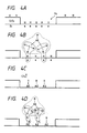
- Figs. 4A - 4D are illustrations for better understanding of the reacion mechanism, and the numbers of H, e and Al shown in Figs. 4A - 4D are not necessarily coincident.
- Si atoms are incorporated into Al during the process of the reaction as described above.
- a low resistivity, dense and flat Al-Si film could be deposited on a substrate.
- Al-Si can be formed with excellent selectivity.
Abstract
Description
- This invention relates to a process for forming a deposited film, particularly a process for forming an Al-Si deposited film which can be preferably applied to electrodes or wiring of a semiconductor integrated circuit device, etc.
- In the prior art, in electronic devices or integrated circuits by use of semiconductors, for electrodes and wiring, aluminum (Al) or a metal containing aluminum as main component such as Al-Si and the like has been primarily used. Al has many advantages such that it is inexpensive and high in electroconductivity, that it can be also internally chemically protected because a dense oxidized film can be formed on the surface, and that it has good adhesion to Si, etc.
- As the method for forming a film for electrodes and wiring of Al or Al-Si as mentioned above, there has been used in the prior art the sputtering method such as magnetron sputtering, etc.
- However, selective deposition and selective growth can not be realized by the sputtering method which has been, used in the prior art. The sputtering is the physical deposition method based on flying of sputtered particles in vacuum, the film thickness at the stepped portion or the insulating film side wall becomes extremely thin, leading to wire breaking in an extreme case. Nonuniformity of film thickness or wire breaking has the drawback that reliability of LSI is markedly lowered.
- On the other hand, since the integration degree of the integrated circuit such as LSI, etc. is increased, and fine formation of wiring or multi-layer wiring has been particularly required in recent years, there is an increasing severe demand not found up to date for Al or Al-Si wiring of the prior art. With finer dimensional formation by increased integration degree, the surface of LSI, etc. is subject to excessive unevenness due to oxidation, diffusion, thin film deposition, and etching, etc. For example, electrodes or wiring metal must be deposited on the surface with a stepped difference, or deposited in a via-hole which is fine in diameter and deep. In 4 Mbit or 16 Mbit DRAM (dynamic RAM), etc., the aspect ratio (via-hole depth/via-hole diameter) of via-hole in which a metal composed mainly of Al such as Al-Si, etc. is to be deposited is 1.0 or more, and the via-hole diameter itself also becomes 1 µm or less. Therefore, even for a via-hole with large aspect ratio, the technique which can deposit an Al-Si compound is required.
- Particularly, for performing sure electrical connection to the device under insulating film such as SiO₂, etc., rather than film formation, Al-Si is required to be deposited so as to embed only the via-hole of the device. In such case, a method of depositing an Al alloy only on Si or metal surface and not depositing it on an insulating film such as SiO₂, etc. is required.
- As the improved sputtering method, there has been developed the bias sputtering method in which a bias is applied on a substrate and deposition is performed so as to embed Al or an Al-Si compound only in the via-hole by utilizing the sputter etching action and the deposition action on the substrate surface. However, since the bias voltage of some 100 V or higher is applied on the substrate, deleterious influence on the device occurs because of charged particle damaging such as change in threshold of MOSFET, etc. Also, because of presence of both etching action and deposition action, there is the problem that the deposition speed cannot be essentially improved.
- In order to solve the problems as described above, various types of CVD (Chemical Vapor Deposition) methods have been proposed. In these methods, chemical reaction of the starting gas in some form is utilized. In plasma CVD or optical CVD, decomposition of the starting gas occurs in gas phase, and the active species formed there further reacts on the substrate to give rise to film formation. In these CVD methods, surface coverage on unevenness on the substrate surface is good. However, carbon atoms contained in the starting gas molecule are incorporated into the film. Also, particularly in plasma CVD, the problem remained that there was damage by charged particles (so called plasma damage) as in the case of the sputtering method.
- The thermal CVD method, in which the film grows through the surface reaction primarily on the substrate surface, is good in surface coverage on unevenness such as stepped portion of the surface, etc. Also, it can be expected that deposition within via-hole will readily occur. Further, wire breaking at the stepped portion can be avoided. Furthermore, there are not caused damages by charged particles which have been observed in the case of the plasma CVD or the sputtering method. The methods of such a kind include, for example, the method seen in Journal of Electrochemical Society, Vol. 131, p. 2175 (1984). In this method triisobutyl aluminum (i-C₄H₉)₃Al (TIBA) is used as organic aluminum gas and an Al film is formed at a film formation temperature of 260 oC and a reaction tube pressure of 0.5 Torr. The substrate temperature is then maintained at about 450°C and SiH₄ is introduced to diffuse Si in the Al film, thus obtaining an Al-Si film.
- When TIBA is to be used, a continuous film can not be obtained unless pretreatment is effected in which prior to film formation, TiCl₄ is flowed to activate the substrate surface to form nuclei. Furthermore, in case where TIBA is used, there is a problem that surface flatness is not sufficient even when TiCl₄ is used. By this method it is not possible to effect selective growth such as Al-Si deposition only in via-holes.
- As another method, there can be mentioned the method described in Japanese Journal of Applied Physics, Vol. 27, No. 11, p. L2134 (1988). In this method, TIBA and Si₂H₆ diluted with Ar gas are supplied, and the gases are heated before TIBA reaches the substrate. By this method, an Al-Si film of a low resistivity can be epitaxially grown on a Si(100) wafer. Although the film obtained by this method has good high quality, there are involved the problems that control is difficult due to necessity of heating the gases and that apparatus for effecting this method is complicated.
- Japanese Laid-Open Patent Application No. 63-33569 describes a method of forming a film by using no TiCl₄, but using in place thereof organic aluminum and heating it in the vicinity of the substrate. According to this method, Al can be deposited selectively only on the metal or semiconductor surface from which the naturally oxidized film has been removed.
- In this case, it is clearly stated that the step of removing the naturally oxidized film on the substrate surface is necessary before introduction of TIBA. Also, it is described that, since TIBA can be used alone, no carrier gas is required to be used, but Ar gas may be also used as the carrier gas. However, the reaction of TIBA with another gas (e.g. H₂) is not contemplated at all, and there is no description of use of H₂ as the carrier gas. Also, in addition to TIBA, trimethyl aluminum (TMA) and triethyl aluminum (TEA) are mentioned, but there is no specific description of other organic metals. This is because, since the chemical properties of organic metals generally vary greatly if the organic substituent attached to the metal element varies little, it is necessary to investigate individually by detailed experimentation to determine what organic metal should be used.
- In the CVD method as described above, not only there is an inconvenience that the naturally oxidized film must be removed, but also there is the drawback that no surface smoothness can be obtained. Also, there is the restriction that heating of the gas is necessary, and yet heating must be done in the vicinity of the substrate. Besides, it must also be experimentally determined at what poximity to the substrate heating must be done, whereby there is also the problem that the place for setting the heater cannot be necessarily freely chosen.
- In the pre-text of the 2nd Symposium of Electrochemical Society, Branch of Japan (July 7, 1989), on page 75, there is a description of film formation of Al according to the double wall CVD method. In this method, TIBA is used and the device is designed so that the gas temperature of TBA can be made higher than the substrate temperature. This method may be also regarded as a modification of the above-mentioned Japanese Laid-open Patent Application No. 63-33569. Also in this method, Al can be selectively grown only on a metal or semiconductor, but not only the difference between the gas temperature and the substrate surface temperature can be controlled with difficulty, but also there is the drawback that the bomb and the pipeline must be heated. Moreover, according to this method, there are involved such problems that no uniform continuous film can be formed, that flatness of the film is poor, etc., unless the film is made thick to some extent.
- As set forth above, the prior art methods have the problems to be solved that it is difficult to obtain a flat Al-Si film of a low resistivity and good quality, that there is considerable limitation in apparatus and in film formation.
- As described above, prior art methods cannot necessarily effect well selective growth of Al-Si, and even if possible, there is a problem with respect to flatness, resistance, purity, etc. of the Al film formed. Also, there has been involved the problem that the film formation method is complicated and can be controlled with difficulty.
- As described above, in the technical field of semiconductors in which higher integration has been desired in recent years, for providing inexpensively a semiconductor device which is more highly integrated and also made higher in performances, there remained many rooms to be improved.
- The present invention has been accomplished in view of the technical tasks as described above, and an object of the present invention is to provide a process for forming a deposited film which can form an Al-Si film of good quality as the electroconductive material at a desired position with good controllability.
- Another object of the present invention is to provide a process for forming a deposited film which can obtain an Al-Si film which has extremely broad general purpose utility and yet is of good quality, without requiring particularly no complicated and expensive deposited film forming device.
- Still another object of the present invention is to provide a process for forming a deposited film which can form an Al-Si film excellent in surface characteristic, electrical characteristics, purity, etc. according to the CVD method utilizing alkyl aluminum hydride, hydrogen, and a gas containing silicon atoms.
- Still another object of the present invenion is to provide a process for forming a deposited film of an Al-Si film which is extremely broad in general purpose utility and excellent in selectivity, without requiring particularly a complicated and expensive deposited film forming device.
- Still another object of the present invention is to provide a process for forming a deposited film which can form an Al-Si film under good selectivity according to the CVD method utilizing alkyl aluminum hydride, hydrogen and a gas containing silicon atoms.
-
- Fig. 1 is a schematic view for illustration of a suitable deposited film forming device in practicing the deposited film forming process according to the process of the present invention.
- Fig. 2 is a schematic view for illustration of another suitable deposited film forming device in practicing the deposited film forming process according to the present invention.
- Figs. 3A - 3E are schematic sectional views for illustration of the deposited film forming process according to one embodiment of the present invention.
- Figs. 4A - 4D are illustrations for explaining the mechanism of Al deposition according to the present invention.
- Preferred embodiments according to the present invention are described in detail below, but the present invention is not limited by these embodiments, and it may have a constitution which accomplishes the object of the present invention.
- One preferred embodiment of the present invention is a process for forming a deposited film comprising the steps of:
- (a) providing a substrate having an electron donative surface (A) in a space for formation of the deposited film;
- (b) introducing a gas of an alkyl aluminum hydride, a gas containing silicon atoms and hydrogen gas into the space for formation of the deposited film; and
- (c) maintaining the temperature of the electron donative surface (A) within the range of from the decomposition temperature of the alkyl aluminum hydride to 450 oC to form an aluminum film containing silicon on the electron donative surface (A).
- Further, another preferred embodiment of the present invention is a process for forming a deposited film comprising the steps of:
- (a) providing a substrate having an electron donative surface (A) and a electron non-donative surface (B) in a space for formation of the deposited film;
- (b) introducing a gas of an alkyl aluminum hydride, a gas containing silicon atoms and hydrogen gas into the space for formation of the deposited film; and
- (c) maintaining the temperature of the electron donative surface (A) within the range of from the decomposition temperature of the alkyl aluminum hydride to 450 oC to form an aluminum film containing silicon selectively on the electron donative surface (A).
- In the following, prior to detailed description, first, the process for forming a deposited film by use of an organic metal is outlined.
- The decomposition reaction of an organic metal, and hence the thin film deposition reaction will vary greatly depending on the kind of the metal atom, the kind of the alkyl bonded to the metal atom, the means of causing the decomposition reaction to occur, the atmospheric gas, etc.
- For example, in the case of M-R₃ (M: the group III metal, R: alkyl group), trimethyl gallium:


- Trimethyl aluminum (TMA) comprising CH₃ groups and Al has a dimer structure at room temperature:

- However, at a high temperature of 300 oC or higher, even if H₂ may be present in the atmosphere, CH₃ group will withdraw H from the TMA molecule, until finally Al-C compound is formed.
- Also, in the case of TMA, in light or a certain region controlled in electric power in H₂ atmosphere high frequency (ca. 13.56 MHz) plasma, C₂H₆ will be formed by the bridging CH₃ between two Al's.
- In essence, since even an organic metal comprising CH₃ group which the simplest alkyl group, C₂H₅ group or iC₄H₉ group and Al or Ga has a reaction mode depending on the kind of the alkyl group, the kind of the metal atom, the excitation decomposition means, for deposition of a metal atom from an organic metal on a desired substrate, the decomposition reaction must be strictly controlled. For example, when Al is to be deposited from triisobutyl aluminum:

- For this reason, a method for controlling precisely both the gas temperature and the substrate temperature has been attempted. However, the device is complicated, and the method is of the sheet treatment type in which deposition can be effected only on one wafer by one deposition process. Besides, since the deposition speed is 500 A/min. at the highest, the throughput necessary for bulk production cannot be realized.
- Similarly, when TMA is employed, Al deposition has been attempted by use of plasma or light, the device also becomes complicated due to use of plasma or light, and also because of the sheet type device, there remains room for improvement for sufficient improvement of throughput.
- Dimethyl aluminum hydride (DMAH) as the alkyl aluminum hydride to be utilized in the present invention is a substance known as alkyl metal, but it could not be estimated at all what Al thin film could be deposited depending on what reaction mode, unless deposited films are formed under all the conditions. For example, in an example of deposition Al by optical CVD from DMAH, the surface morphology is inferior, and the resistivity value was greater than the bulk value (2.7 µohm·cm) as several µohm to 10 µohm cm, thus being inferior in film quality.
- Now, referring to the drawings, preferred embodiments of the present invention are described in more detail.
- In the present invention, for depositing an Al-Si film of good quality as the electroconductive deposition film on a substrate, the CVD method is used.
- More specifically, by use of dimethyl aluminum hydride (DMAH):


- As the substrate applicable in the present invention, a material having electron donative property may be employed.
- The electron donative material is described in detail below.
- The electron donative material refers to one having free electrons existing or free electrons intentionally formed in the substrate, for example, a material having a surface on which the chemical reaction is promoted through give-and-take of electrons with the starting gas molecules attached on the substrate surface. For example, generally metals and semiconductors correspond to such material. Those having very thin oxidized film on the metal or semiconductor surface are also included. For, with such thin film, the chemical reaction can occur between the substrate and the attached starting molecules.
- Specifically, there may be included semiconductors such as single crystalline silicon, polycrystalline silicon, amorphous silicon, etc., binary system or ternary system or quaternary system III-V compound semiconductors comprising combinations of Ga, In, Al as the group III element and P, As, N as the group V element, or II-IV compound semiconducters, or metals themselves such as tungsten, molybdenum, tantalum, aluminum, titanium, copper, etc., or silicides of the above metals such as tungsten silicide, molybdenum silicide, tantalum silicide, aluminum silicide, titanium silicide, etc., further metals containing either one of the constituent of the above metals such as aluminum silicon, aluminum titanium, aluminum copper, aluminum tantalum, aluminum silicon copper, aluminum silicon titanium, aluminum palladium, titanium nitride, etc.
- On the substrate with such constitution, Al is deposited only through simple thermal reaction in the reaction system of the starting gas and H₂. For example, the thermal reaction in the reaction system between DMAH and H₂ may be basically considered as follows:

- Since MMAH₂ has low vapor pressure as 0.01 to 0.1 Torr at room temperature, a large amount of the starting material can be transported with difficulty, and the upper limit value of the deposition speed is several hundred Å/min. in the present embodiment, and preferably, it is most desirable to use DMAH of which vapor pressure is 1 Torr at room temperature.
- In another embodiment of the present invention, the CVD method is used for selective deposition of a good Al film as the electroconductive deposition film on the substrate.
- More specifically, as described above, by use of dimethyl aluminum hydride (DMAH) or monomethyl aluminum hydride (MMAH₂), a gas containing Si atoms as the starting gas and H₂ as the reaction gas, an Al-Si film is selectively formed on the substrate by gas phase growth with a gas mixture of these.
- The substrate applicable in the present invention has a first substrate surface material for formation of the surface on which Al-Si is deposited, and a second substrate surface material on which no Al-Si is deposited. And, as the first substrate surface material, a material having the electron donative surface is used.
- In contrast, as the material for forming the surface on which Al-Si is not deposited selectively, namely the material for forming the electron non-donative surface, conventional insulating materials, oxidized silicon formed by thermal oxidation, CVD, etc., glass or oxidized film such as BSG, PSG, BPSG, etc., thermally nitrided film, silicon nitrided film by plasma CVD, low pressure CVD, ECR-CVD method, etc.
- Fig. 1 is a schematic view showing a preferable deposition film forming device for applying the present invention.
- Here, 1 is a substrate for forming an Al-Si film. The substrate 1 is mounted on a
substrate holder 3 provided internally of thereaction tube 2 for forming a space for formation of a deposited film which is substantially closed to Fig. 1. As the material constituting thereaction tube 2, quartz is preferable, but it may be also made of a metal. In this case, it is preferable to cool the reaction tube. Thesubstrate holder 3 is made of a metal, and is provided with a heater 4 so that the substrate mounted thereon can be heated. And, the constitution is made so that the substrate temperature can be controlled by controlling the heat generation temperature of the heater 4. - The feeding system of gases is constituted as described below.
- 5 is a gas mixer, in which the first starting gas, the second starting gas and the reaction gas are mixed, and the mixture is fed into the
reaciton tube 2. 6 is a starting gas gasifier provided for gasification of an organic metal as the first starting gas. - The organic metal to be used in the present invention is liquid at room temperature, and is formed into saturated vapor by passing a carrier gas through the liquid of the organic metal within the
gasifier 6, which is in turn introduced into themixer 5. - The evacuation is constituted as described below.
- 7 is a gate valve, which is opened when performing evacuation of a large volume such as during evacuation internally of the
reaction tube 2 before formation of the deposited film. 8 is a slow leak valve, which is used when performing evacuation of a small volume such as in controlling the pressure internally of thereaction tube 2 during formation of the deposited film. 9 is an evacuation unit, which is constituted of a pump for evacuation such as turbo molecular pump, etc. - The conveying system of the substrate 1 is constituted as described below.
- 10 is a substrate conveying chamber which can house the substrate before and after formation of the deposited film, which is evacuated by opening the
valve 11. 12 is an evacuation unit for evacuating the conveying chamber, which is constituted of a pump for evacuation such as turbo molecular pump, etc. - The
valve 13 is opened only when the substrate 1 is transferred between the reaction chamber and the conveying space. - As shown in Fig. 1, in the starting
gas gasifier 6 which is the gas formation chamber for forming the starting gas, the liquid DMAH maintained at room temperature is bubbled with H₂ or Ar (or other inert gas) as the carrier gas to form gaseous DMAH, which is transported to themixer 5. The H₂ gas as the reaction gas is transported through another route into themixer 5. The gases are controlled in flow rates so that the respective partial pressures may become desired values. - In the case of forming a film by this device, the first starting gas may be of course MMAH₂, but DMAH with a vapor pressure enough to become 1 Torr at room temperature is the most preferred. Also, DMAH and MMAH₂ may be used in a mixture.
- As the second starting gas containing Si, there can be used Si₂H₆, SiH₄, Si₃H₈, Si(CH₃)₄, SiCl₄, SiH₂Cl₂ and SiH₃Cl. Of these compounds, Si₂H₆ which can be easily decomposed at the low temperature of 200 - 300°C. The gases such as Si₂H₆ are diluted with H₂ or Ar and transported to the
mixer 5 through a system other than the DMAH system. - The deposited film formed at a substrate temperature of 160 oC to 450 oC by use of such starting gas and reaction gas, with a thickness of for example 400 Å, has a resistivity at room temperature of 2.7 - 3.0 µohm·cm which is substantially equal to Al bulk resistivity, and is a continuous and flat film. At this time, the pressure during film formation can be chosen within the range from 10⁻³ Torr to 760 Torr. Also, even when the film thickness may be 1 µm, its resistivity is ca. 2.7 - 3.0 µohm·cm, and a sufficiently dense film can be formed also with a relatively thicker film. Also, the reflectance in the visible light wavelength region is approximately 80 %, whereby a thin film excellent in surface flatness can be deposited.
- The substrate temperature is desirably the decomposition temperature of the starting gas containing Al or higher, and 450 oC or lower as described above, but specifically the substrate temperature of 200 to 450 oC is more desirable, and when deposition is carried out under this condition, by making the DMAH
partial pressure 10⁻⁴ to 10⁻³ Torr, the deposition speed becomes very great as 100 Å/min. to 800 Å/min., whereby sufficient great deposition speed corresponding to the cost as the Al-Si deposition technique for ultra-LSI can be obtained. - A more preferable substrate temperature condition is 270 oC to 350 oC, and the Al-Si film deposited under this condition is also strongly orientatable and, even when subjected to the heat treatment at 450 oC for 1 hour, the Al-Si film on the Si monocrystalline or Si polycrystalline substrate becomes a good Al-Si film without generation of hillock, spike as seen in the film forming method of the prior art. Also, such Al-Si film is excellent in electro-migration resistance.
- In the device shown in Fig. 1, Al-Si can be deposited on only one sheet of substrate in deposition for one time. Although a deposition speed of ca. 800 Å/min. can be obtained, it is still insufficient for performing deposition of a large number of sheets within a short time.
- As the deposition film forming device for improving this point, there is the low pressure CVD device which can deposit Al-Si by simultaneous mounting of a large number of sheets of wafer. Since the Al-Si film formation according to the present invention utilizes the surface reaction on the electron donative substrate surface, in the hot wall type low pressure CVD method wherein only the' substrate is heated, Al can be deposited on the substrate by use of DMAH and H₂ and the Si starting gas such as Si₂H₆, etc.
- The reaction tube pressure may be 0.05 to 760 Torr, desirably 0.1 to 0.8 Torr, the substrate temperature 160 oC to 450 oC, desirably 200 oC to 400 oC, the DMAH partial pressure 1 x 10⁻⁵-fold to 1.3 x 10⁻³-fold of the pressure in the reaction tube, the Si₂H₆ partial pressure 1 x 10⁻⁷-fold to 1 x 10⁻⁴-fold of the pressure in the reaction tube, and under such conditions, Al-Si can be well deposited on the electron donative substrate.
- Fig. 2 is a schematic illustration showing a deposited film forming device to which such present invention is applicable.
- 57 is a substrate for formation of Al-Si film. 50 is an outside reaction tube made of quartz for forming a space for formation of deposited film substantially closed to the surrounding, 51 an innerside reaction tube made of quartz located for separating the flow of gas within the
outside reaction tube 50, 54 a flange made of a metal for opening and closing of the opening of theoutside reaction tube 50, and thesubstrate 57 is located within thesubstrate holding member 56 provided internally of theinnerside reaction tube 51. Thesubstrate holding member 56 should be preferably made of quartz. - Also, in the present device, the substrate temperature can be controlled by the
heater portion 59. The pressure internally of thereaction tube 50 is constituted so as to be controllable by the evacuation system connected through thegas evacuation outlet 53. - The gas feeding system is constituted to have a first gas system, a second gas system, a third gas system and a mixer (none are shown in Fig. 2) similarly as the device shown by the
symbols reaction tube 50 through the startinggas inlet 52. These gases react on the surface of thesubstrate 57 during passage internally of theinnerside reaction tube 51 as shown by thearrowhead 58 in Fig. 2 to deposit Al-Si on the substrate surface. The gases after the reaction pass through the gap formed between theinnerside reaction tube 51 and theoutside reaction tube 50, and evacuated through thegas evacuation outlet 53. - In taking out and in the substrate, the
flange 54 made of a metal is permitted to fall by an elevator (not shown) together with thesubstrate holding member 56 and thesubstrate 57 to be moved to a predetermined position where the substrate is mounted and detached. - By forming a deposited film under the conditions as described above by use of such device, Al-Si films of good quality can be formed in all the wafers within the device.
- As described above, the film obtained according to the Al-Si film formation process based on the embodiment of the present invention is dense with little content of impurity such as carbon, etc. and resistivity which is similar to bulk, and also has high surface smoothness, and therefore remarkable effects as described below can be obtained.
- Hillock is occurrence of concavities on the Al-Si surface due to partial migration of Al-Si when inner stress during film formation is released in the heat treatment step. Also, similar phenomenon occurs by local migration by current passage. The Al-Si film formed by the present invention has little inner stress and is approximate to the state of monocrystal. For this reason, in the heat treatment at 450 °C for one hour, as contrasted to formation of 10⁴ - 10⁶/cm² of hillocks in the Al-Si film of the prior art, the hillock number could be greatly improved as 0 to 10/cm². Thus, due to substantial absence of Al-Si surface concavity, the resist film thickness and the interlayer insulating film can be made thin to be advantageous for making it finer and more flat.
- Electro-migration is the phenomenon that the wiring atoms move by passage of a current of high density. By this phenomenon, voids are generated and grown along the grain boundary, whereby as accompanied with reduction of the cross-sectional area, the wiring generates heat to be broken. In the prior art, the anti-migration property has been improved by adding Cu, Ti, etc. to Al-Si to form an alloy. However, the alloy formation results in complication of the etching step and difficulty of minute formation.
- Migration resistance is generally evaluated by average wiring life.
- The wiring formed by the sputtering method or the CVD method of the prior art has obtained anaverage wiring life of 1 x 10² to 10³ hours (in the case of a wiring cross-sectional area of 1 µm²) under the current passage test conditions of 250 °C, 1 x lo⁶ A/cm². In contrast, the Al-Si film obtained by the Al-Si film formation method based on the embodiment of the present invention could obtain an average wiring life of 10³ to 10⁴ hours with a wiring having a cross-sectional area of 1 µm².
- Hence, according to the present invention, for example, when the wiring width is 0.8 µm, a wiring layer thickness of 0.3 µm can sufficiently stand practical application. That is, since the wiring layer thickness can be made thinner, unevenness on the semiconductor surface after arrangement of wiring can be suppressed minimum, and also high reliability in passing ordinary current can be obtained. Also, this is possible by a very simple process.
- By the heat treatment in the wiring step, eutectic reaction between Al in the wiring material and Si in the substrate may occur to result in penetration of Al-Si eutectic called as alloy pit into the substrate in spike pattern, thereby destroying shallow junction.
- As countermeasure, it is general to employ a material other than pure Al when the depth of junction is 0.3 µm or more and to employ barrier metal technique of Ti, W, Mo type.
- However, there remain some points to be improved such as complication of etching, rise of contact resistivity and the like. In Al-Si formed according to the present invention, generation of alloy pits in contact portion with substrate crystal due to heat treatment in the wiring step can be inhibited and wiring with good contact can also be obtained. In other words, wiring can be effected only with an Al-Si material without destroying junction even when the junction is formed in a depth of about 0.1 µm.
- In the prior art, roughness of the surface of a metal thin film had inconvenience in the alignment step for the mask and the substrate in the patterning step and in the etching step.
- That is, there is unevenness extending to several µm on the surface of Al film according to the prior art method, whereby the surface morphology is poor, and therefore had the following disadvantages.
- 1) Alignment signals cause diffused reflection to occur at the surface, whereby noise level becomes higher and inherent alignment signals cannot be discriminated.
- 2) For covering large surface unevenness, the resist film thickness must be taken large, which is opposite to fine formation.
- 3) If the surface morphology is poor, halation due to the resist internal reflection will occur locally, whereby resist remaining occurs.
- 4) If the surface morphology is poor, the side wall becomes notched in the wiring etching step according to its unevenness.
- According to the present invention, the surface morphology of Al-Si film to be formed is markedly improved to cancell all the drawbacks described above.
- In other words, in the patterning step, at the line width of the resolving power limit of the exposure machine, the
alignment precision 3 =0.15 µm can be accomplished, whereby wiring having smooth side plane is rendered possible without causing halation to occur. - In the prior art method, if the size of the contact hole becomes finer as 1 µm x 1 µm or less, Si in the wiring is precipitated on the substrate of the contact hole during heat treatment in the wiring step to cover thereover, whereby resistance between the wiring and the element becomes markedly larger.
- According to the embodiment of the present invention, since a dense film is formed according to the surface reaction, Al-Si has been confirmed to have a resistivity of 2.7 - 3.3 µohm cm. Also, the contact resistivity can attain 1 x 10⁻⁶ ohm·cm² at an area of 0.6 µm x 0.6 µm when the Si portion has an impurity of 10²⁰ cm⁻³.
- That is, according to the present invention, a good contact with the substrate can be obtained.
- As described in detail above, by applying the present invention to the wiring formation method of a semiconductor integrated circuit, the yield can be improved, and reduction of cost can be promoted to great extent as compared with Al wiring of the prior art.
- Figs. 3A - 3E show how the Al-Si film according to the present invention is selectively grown.
- Fig. 3A is an illustration showing schematically the cross-section of the substrate before formation of the Al-Si deposited film according to the present invention. 90 is the substrate comprising an electron donative material, and 91 a thin film comprising an electron non-donative material.
- In the case of using DMAH and Si₂H₆ as the starting gases, when a gas mixture containing H₂ as the reaction gas is fed onto the substrate 1 heated within a temperature range from the decomposition temperature of DMAH to 450 oC, Al is precipitated on the
substrate 90, whereby a continuous film of Al is formed as shown in Fig. 3B. Here, the pressure within thereaction tube 2 should be desirably 10⁻³ to 760 Torr, and the DMAH partial pressure preferably 1.5 x 10⁻⁵ to 1.3 x 10⁻³-fold of the pressure within the above reaction tube. The Si₂H₆ partial pressure should preferably be 1 x 10⁻⁷ to 1 x 10⁻⁴-fold of the pressure within thereaction tube 2. - When deposition of Al-Si is continued under the above conditions, via the state of Fig. 3C, the Al-Si film grows to the level of the uppermost portion of the
thin film 91 as shown in Fig. 3D. Further, when grown under the same conditions, as shown in Fig. 3E, the Al-Si film can grow to 5000 Å substantially without growth in the lateral direction. This is the most characteristic point of the deposited film obtained by the present invention, and it will be understood how a film of good quality can be formed under good selectivity. - As the result of analysis according to Auger's electron spectroscopy or photoelectric spectroscopy, no entrainment of an impurity such as carbon or oxygen is recognized in this film.
- The deposited film thus formed has a resistivity of, for example, with a film thickness of 400 Å, 2.7 - 3.0 µohm·cm at room temperature which is substantially equal to the bulk resistivity of Al, and becomes continuous and flat film. Also, even with a film thickness of 1 µm, its resistance at room temperature is approximately 2.7 - 3.0 µohm₇cm and a sufficiently dense film is, formed with a relatively thicker film. The reflectance in the visible wavelength region is approximately 80 %, and a thin film with excellent surface flatness can be deposited. The substrate temperature in performing such selective deposition should be desirably the decomposition temperature of the starting gas containing Al or higher and 450 oC or lower as mentioned above, but specifically a substrate temperature of 200 to 450 oC is desirable, and when deposition is performed under such condition, the deposition speed is sufficiently great as 100 Å/min. to 800 Å/min. when DMAH partial pressure is 10⁻⁴ to 10⁻³ Torr. Thus a sufficiently great deposition speed can be obtained as the Al-Si deposition technique for ultra-LSI.
- A more preferable substrate temperature condition is 270 oC to 350 oC, and the Al-Si film deposited under this condition is also strongly orientatable and, even when subjected to the heat treatment at 450 oC for 1 hour, the Al-Si film on the Si monocrystalline or Si polycrystalline substrate becomes a good Al-Si film without generation of hillock, spike. Also, such Al-Si film is excellent in electro-migration resistance.
- In the device shown in Fig. 1, Al-Si can be deposited on only one sheet of substrate in deposition for one time. Although a deposition speed of ca. 800 Å/min. can be obtained, it is still insufficient for performing deposition of a large number of sheets within a short time.
- As the deposition film forming device for improving this point, there is the low pressure CVD device which can deposit Al-Si by simultaneous mounting of a large number of sheets of wafer. Since the Al-Si deposition according to the present invention utilizes the surface reaction of the electron donative substrate surface, in the hot wall type low pressure CVD method wherein only the substrate is heated, a Al-Si compound containing 0.5 to 2.0 % of Si can be deposited on the substrate by adding DMAH, H₂ and a Si starting gas such as Si₂H₆, etc.
- The reaction tube pressure may be 0.05 to 760 Torr, desirably 0.1 to 0.8 Torr, the substrate temperature 160 oC to 450 oC, desirably 200 oC to 400 oC, the DMAH partial pressure 1 x 10⁻⁵-fold to 1.3 x 10⁻³-fold of the pressure in the reaction tube, the Si₂H₆ partial pressure 1 x 10⁻⁷-fold to 1 x 10⁻⁴-fold of the pressure in the reaction tube, and under such conditions, Al-Si can be selectively deposited on only the electron donative substrate. In the case of such selective deposition, a good Al-Si film can also be formed under the above described conditions by use of the deposited film forming apparatus such as described above by referring to Figs. 1 and 2.
- As described above, the film obtained according to the Al-Si film selective formation process based on the embodiment of the present invention is dense with very little content of impurity such as carbon, etc. and resistivity which is similar to bulk, and also has high surface smoothness, and therefore remarkable effects as described below can be obtained.
- The Al-Si film formed according to the present invention has little internal stress and is approximate to the state of monocrystal. For this reason, in the heat treatment at 450 oC for one hour, as contrasted to formation of 10⁴ - 10⁶/cm² of hillocks in the Al-Si film of the prior art, the hillocks number could be greatly improved as 0 to 10/cm².
- In the prior art, the anit-migration property has been improved by adding Cu, Ti, etc. to Al-Si to form an alloy. However, the alloy formation results in complication of the etching step and difficulty of minute formation.
- The wiring formed by the method of the prior art has obtained an average wiring life of 1 x 10² to 10³ hours (in the case of a wiring cross-sectional area of 1 µm²) under the current passage test conditions of 250 oC, 1 x 10⁶ A/cm². In contrast, the Al-Si film obtained by the Al-Si film selective formation method based on the embodiment of the present invention could obtain an average wiring life of 10³ to 10⁴ hours with a wiring having a cross-sectional area of 1 µm².
- The Al-Si selectively formed according to the present invention can suppress generation of alloy pit at the contact portion with the substrate crystal even by the heat treatment during wiring step, and also a wiring with good contact characteristic can be obtained. That is, even when the junction is made shallow to the extent of 0.1 µm, the junction will not be destroyed with only the Al-Si material.
- According to the present invention, the surface morphology of the Al-Si film to be formed can be improved epoch-makingly, whereby all of the problems of the prior art can be improved.
- According to the present invention, since adense film is selectively formed by the surface reaction even when the opening may be 1 µm x 1 µm or less, it has been confirmed that the Al-Si completely filled within the contact hole and through hole each has a resistivity of 2.7 - 3.3 µohm·cm. Also, the contact resistivity can attain 1 x 10⁻⁶ ohm·cm² in the case where the Si portion has an impurity of 10²⁰cm⁻³ in a hole of 0.6 µm x 0.6 µm.
- That is, according to the present invention, the wiring material can be completely embedded only in the minute opening, and also good contact with the substrate can be obtained. Therefore, the present invention can contribute greatly to improvement of resistance within hole and contact resistance which have been the greatest problems in the fine process of 1 µm or less.
- As described in detail above, by applying the present invention to the wiring formation method of a semiconductor integrated circuit, particularly embedding of contact hole or through hole, the yield can be improved, and reduction of cost can be promoted to great extent as compared with Al-Si wiring of the prior art.
- First, the procedure for Al-Si film formation is as follows. By use of the device shown in Fig. 1, the
reaction tube 2 is internally evacuated to ca. 1 x 10⁻⁸ Torr by the evacuation unit 9. However, Al-Si film can be also formed if the vacuum degree within thereaction tube 2 may be worse than 1 x 10⁻⁸ Torr. - After washing of Si wafer, the conveying
chamber 10 is released to atmospheric pressure and Si wafer is mounted in the conveying chamber. The conveying chamber is evacuated to ca. 10⁻⁶ Torr, and then thegate valve 13 is opened and the wafer is mounted on thewafer holder 3. - After mounting of the wafer on the
wafer holder 3, thegate valve 13 is closed, and thereaction chamber 2 is evacuated to a vacuum degree of ca. 1 x 10⁻⁸ Torr. - In this Example, DMAH is fed through the first gas line. As the carrier gas of DMAH line H₂ which is the same as the reaction gas is employed. The second gas line is used for H₂ and the third gas line for Si₂H₆.
- By passing H₂ through the second gas line, the pressure within the
reaction tube 2 is made a predetermined value by controlling the opening of the slow leak valve 8. A typical pressure in this Example is made approximately 1.5 Torr. Then, the wafer is heated by current passage through the heater 4. After the wafer temperature has reached a predetermined temperature, DMAH and Si₂H₆ are introduced into the reaction tube through the DMAH line and the Si₂H₆ line. The total pressure is ca. 1.5 Torr, and the DMAH partial pressure is made ca. 1.5 x 10⁻⁴ Torr. The Si₂H₆ partial pressure is made 2 x 10⁻⁶ Torr. When Si₂H₆ and DMAH are introduced into thereaction tube 2, Al-Si is deposited. After a predetermined deposition time has elapsed, feeding of DMAH and Si₂H₆ is stopped. Next, heating of the heater 4 is stopped to cool the wafer. Feeding of H₂ gas is stopped, and after evacuation internally of the reaction tube, the wafer is transferred to the conveying chamber, and only the conveying chamber is made atmospheric before taking out the wafer. The outline of Al-Si film formation is as described above. - Al-Si films were deposited at the respective temperatures each for 10 sheet samples following the same procedure as described in Example 1 under the following conditions:
Total pressure: 1.5 Torr
DMAH partial pressure: 1.5 x 10⁻⁴ Torr
Si₂H₆ partial pressure: 2 x 10⁻⁶ Torr. - The Al-Si films deposited by varying the substrate temperature at 13 levels were evaluated by use of various evaluation methods. The results are shown in Table 1.
- It has been confirmed from the results that films of extremely excellent quality can be obtained within the temperature range of 160 to 450 °C, more preferably 200 to 400 °C, optimally 270 to 350 °C.


- Following the same procedure as in Example 1 to set the parameters as follows:
Total pressure: 1.5 Torr
DMAH partial pressure: 5 x 10⁻⁴ Torr
Substrate temperature (Tsub): 300 °C
and the Si₂H₆ partial pressure was varied from 1.5 x 10⁻⁷ Torr to 1 x 10⁻⁴ Torr to effect deposition. The Si content (wt.%) of the Al-Si films were varied from 0.005 % to 5 % approximately in proportion to the Si₂H₆ partial pressure. As to resistivity, carbon content, average wiring life, deposition speed, hillock density and spike generation, the same results as in Experimental example 1 were obtained. However, in samples having a Si content of 4 % or higher, deposition was generated in the films which appeared to be Si to worsen surface morphology, thereby making the reflectance 65 % or lower. Samples having a Si content of less than 4 % exhibited a reflectance of 80 to 95 %, which was the same as in Experimental example 1. - First, the procedure of Al-Si film formation is as follows. By the evacuation unit 9, the reaction tube is evacuated internally to ca. 1 x 10⁻⁸ Torr. Al-Si film can be formed even if the vacuum degree in the
reaction tube 2 may be higher than 1 x 10⁻⁸ Torr. - After washing of the Si wafer, the conveying
chamber 10 is released to atmospheric pressure and the Si wafer is mounted in the conveying chamber. The conveying chamber is evacuated to ca. 1 x 10⁻⁶ Torr, then thegate valve 13 is opened and the wafer is mounted on thewafer holder 3. - After mounting of the
wafer holder 3, thegate valve 13 is evacuated to a vacuum degree in thereaction chamber 2 of ca. 1 x 10⁻⁸ Torr. - In this Example, the first gas line is used for DMAH. As the carrier gas for the DMAH line, Ar is employed. The second gas line is used for H₂. The third gas line is provided for Si₂H₆.
- By passing H₂ through the second gas line, the pressure within the
reaction tube 2 is made a predetermined value by controlling the opening of the slow leak valve 8. A typical pressure in this Example is made approximately 1.5 Torr. Then, the wafer is heated by current passage through the heater 4. After the wafer temperature has reached a predetermined temperature, DMAH and Si₂H₆ are introduced into the reaction tube through the DMAH line and the Si₂H₆ line. The total pressure is ca. 1.5 Torr, and the DMAH partial pressure is made ca. 1.5 x 10⁻⁴ Torr. The Si₂H₆ partial pressure is made 2 x 10⁻⁵ Torr. When Si₂H₆ and DMAH are introduced into thereaction tube 2, Al-Si is deposited. After a predetermined deposition time has elapsed, feeding of DMAH and Si₂H₆ is stopped. Next, heating of the heater 4 is stopped to cool the wafer. Feeding of H₂ gas is stopped, and after evacuation internally of the reaction tube, the wafer is transferred to the conveying chamber, and only the conveying chamber is made atmospheric pressure before taking out the wafer. The outline of Al-Si film formation is as described above. - For deposited films formed according to the method of Example 2, concerning resistivity, carbon content, average wiring life, deposition speed, hillock density, generation of spike and reflectance, the same results as in Example 1 were obtained.
- Following the same procedure as in Example 2 to set the parameters as follows:
Total pressure: 1.5 Torr
DMAH partial pressure: 5 x 10⁻⁴ Torr
Substrate temperature (Tsub): 300 °C
and the Si₂H₆ partial pressure was varied from 1.5 x 10⁻⁷ Torr to 1 x 10⁻⁴ Torr to effect deposition. The Si content (wt.%) of the Al-Si films were varied from 0.005 % to 5 % approximately in proportion to the Si₂H₆ partial pressure. As to resistivity, carbon content, average wiring life, deposition speed, hillock density and spike generation, the same results as in Experimental example 1 were obtained. However, in samples having a Si content of 4 % or higher, deposition was generated in the films which appeared to be Si to worsen surface morphology, thereby making the reflectance 65 % or lower. Samples having a Si content of less than 4 % exhibited a reflectance of 80 to 95 %, which was the same as in Experimental example 1. - This Example 3 is film formation according to the low pressure CVD method.
- A silicon substrate was placed in the low pressure CVD method shown in Fig. 2, and Al-Si film was formed within the same badge. The film formation conditions were made a reaction tube pressure of 0.3 Torr, a DMAH partial pressure of 3.0 x 10⁻⁵ Torr, a Si₂H₆ partial pressure of 1.0 x 10 Torr, a substrate temperature of 300 oC, and a film formation time of 10 minutes.
- As the result of film formation under such conditions, an Al-Si film of 7000 Å was deposited. The film quality was very good, exhibiting the sameproperties as one prepared at a substrate temperature of 300 oC shown in Experimental example 1.
- This Example 4 shows a film formation method using MMAH₂ in place of DMAH.
- The procedure of Example 1 was repeated to effect deposition with the exception that MMAH₂ was used as the starting gas and the parameters were set as follows:
Total pressure: 1.5 Torr
MMAH₂ partial pressure: 5 x 10⁻⁴ Torr
Si₂H₆ partial pressure: 1.0 x 10⁻⁵ Torr - As a result, Al-Si thin films were deposited within the substrate temperature range of 160 °C to 400 °C which contained no carbon impurity and were excellent in flatness and denseness similarly as in Experimental example 1.
- This Example 5 performs deposition using a gas other than Si₂H₆ as a gas of the compound containing silicon atoms.
- The procedure of Example 1 was repeated to effect deposition with the exception that SiH₄ was used in place of Si₂H₆ as the starting material containing Si and the parameters were set as follows:
Total pressure: 1.5 Torr
DMAH partial pressure: 5 x 10⁻⁴ Torr
SiH₄ partial pressure: 1 x 10⁻⁵ Torr - As a result, Al-Si thin films were deposited within the substrate temperature range of 160 °C to 400 °C which contained no carbon impurity and were excellent in flatness and denseness similarly as in Experimental example 1.
- Examples 6 to 8 and Experimental examples 8 to 15 described below are examples when forming Al-Si films selectively.
- In this Example 6, selective deposition of Al-Si is effected by use of the device shown in Fig. 1. The
reaction tube 2 is internally evacuated to ca. 1 x 10⁻⁸ Torr by the evacuation unit 9. However, Al-Si film can be also formed even if the vacuum degree within thereaction tube 2 may be worse than 1 x 10⁻⁸ Torr. - After washing of the Si wafer, the conveying
chamber 10 is released to atmospheric pressure and the Si wafer is mounted in the conveying chamber. The conveying chamber is evacuated to ca. 1 x 10⁻⁶ Torr, then thegate valve 13 is opened and the wafer is mounted on thewafer holder 3. - After mounting of the wafer on the
wafer holder 3, thegate valve 13 is closed, and thereaction chamber 2 is evacuated to a vacuum degree of ca. 1 x 10⁻⁸ Torr. - In this Example, DMAH is fed through the first gas line. As the carrier gas of DMAH line, H₂ is employed. The second gas line is used for H₂ and the third gas line for Si₂H₆. By passing H₂ through the second gas line, the pressure within the
reaction tube 2 is made a predetermined value by controlling the opening of the slow leak valve 8. A typical pressure in this Example is made approximately 1.5 Torr. Then, the wafer is heated by current passage through the heater 4. After the wafer temperature has reached a predetermined temperature, DMAH and Si₂H₆ are introduced into the reaction tube through the DMAH line and the Si₂H₆ line. The total pressure is ca. 1.5 Torr, and the DMAH partial pressure is made ca. 1.5 x 10⁻⁴ Torr. The Si₂H₆ partial pressure is made 2 x 10⁻⁶ Torr. When Si₂H₆ and DMAH are introduced into thereaction tube 2, Al-Si is deposited. After a predetermined deposition time has elapsed, feeding of DMAH and Si₂H₆ is stopped. Next, heating of the heater 4 is stoppedto cool the wafer. Feeding of H₂ gas is stopped, and after evacuation internally of the reaction tube, the wafer is transferred to the conveying chamber, and only the conveying chamber is made atmospheric before taking out the wafer. The outline of Al-Si film formation is as described above. - Si substrates (N type, 1 - 2 ohm·cm) were subjected to thermal oxidation at a temperature of 1000 oC according to the hydrogen combustion system (H₂: 4 liters/M, O₂: 2 liters/M).
- The film thickness was 7000 Å ± 500 Å, and the refractive index 1.46. A photoresist was coated on the whole Si substrate, and a desired pattern was baked by an exposure machine. The pattern was such that various holes of 0.25 µm x 0.25 µm - 100 µm x 100 µm were opened. After development of the resist, with the photoresist as the mask, the subbing SiO₂ was etched by the reactive ion etching (RIE), etc. to have the substrate Si partially exposed. Thus, 130 sheets of samples having various sizes of SiO₂ holes of 0.25 µm x 0.25 µm - 100 µm x 100 µm were prepared, the substrate temperature was set at 13 levels, and for the samples each of 10 sheets at the respective temperatures, Al-Si films were selectively deposited following the procedure as described above under the following conditions:
Total pressure: 1.5 Torr
DMAH partial pressure: 1.5 x 10⁻⁴ Torr
Si₂H₆ partial pressure: 2 x 10⁻⁶ Torr - The Al-Si films deposited by varying the substrate temperature at 13 levels were evaluated by use of various evaluation methods. The results are shown in Table 2.


- In the above samples, no Al-Si was deposited on SiO₂ at a temperature range from 160 oC to 450 oC, and Al-Si was deposited only on the portion with opening of SiO₂ to have Si exposed. Also, when deposition was carried out in the above temperature range continuously for 2 hours, similar selective depositablity was maintained.
- Following the same procedure as in Example 1 to set the parameters as follows:
Total pressure: 1.5 Torr
DMAH partial pressure: 5 x 10⁻⁴ Torr
Substrate temperature (Tsub): 300 °C
and the Si₂H₆ partial pressure was varied from 1.5 x 10⁻⁷ Torr to 1 x 10⁻⁴ Torr to effect deposition. The Si content (wt.%) of the Al-Si films were varied from 0.005 % to 5 % approximately in proportion to the Si₂H₆ partial pressure. As to resistivity, carbon content, average wiring life, deposition speed, hillock density and spike generation, the same results as in Experimental example 8 were obtained. However, in samples having a Si content of 4 % or higher, deposition was generated in the films which appeared to be Si to worsen surface morphology, thereby making the reflectance 65 % or lower. Samples having a Si content of less than 4 % exhibited a reflectance of 80 to 95 %, which was the same as in Experimental example 8. - Furthermore, similarly as in Experimental example 8 selective depositability depending on substrate surface material was also confirmed over the entire region.
- First, the procedure of Al-Si film formation is as follows. By the evacuation unit 9, the
reaction tube 2 is evacuated internally to ca. 1 x 10⁻⁸ Torr. Al-Si film can be formed even if the vacuum degree in thereaction tube 2 may be worse than 1 x 10⁻⁸ Torr. - After washing of the Si wafer, the conveying
chamber 10 is released to atmospheric pressure and the Si wafer is mounted in the conveying chamber. The conveying chamber is evacuated to ca. 1 x 10⁻⁶ Torr, then thegate valve 13 is opened and the wafer is mounted on thewafer holder 3. - After mounting of the
wafer holder 3, thegate valve 13 is closed and evacuated to a vacuum degree in thereaction chamber 2 of ca. 1 x 10⁻⁸ Torr. - In this Example, the first gas line is used for DMAH. As the carrier gas for the DMAH line, Ar is employed. The second gas line is used for H₂. The third gas line is provided for Si₂H₆.
- By passing H₂ through the second gas line, the pressure within the
reaction tube 2 is made a predetermined value by controlling the opening of the slow leak valve 8. A typical pressure in this Example is made approximately 1.5 Torr. Then, the wafer is heated by current passage through the heater 4. After the wafer temperature has reached a predetermined temperature, DMAH and Si₂H₆ are introduced into the reaction tube through the DMAH line and the Si₂H₆ line. The total pressure is ca. 1.5 Torr, and the DMAH partial pressure is made ca. 1.5 x 10⁻⁴ Torr. When Si₂H₆ and DMAH are introduced into thereaction tube 2, Al-Si is deposited. After a predetermined deposition time has elapsed, feeding of DMAH and Si₂H₆ is stopped. Next, heating of the heater 4 is stopped to cool the wafer. Feeding of H₂ gas is stopped, and after evacuation internally of the reaction tube, the wafer is transferred to the conveying chamber, and only the conveying chamber is made atmospheric before taking out the wafer. The outline of Al-Si film formation is as described above. - Al-Si films were formed according to the method of Example 7. For the deposited films obtained, concerning resistivity, carbon content, average wiring life, deposition speed, hillock density, generation of spike and reflectance, the same results as in Experimental example 8 were obtained.
- Also, selective depositability with substrate was the same as in Experimental example 8.
- Following the same procedure as in Example 7 to set the parameters as follows:
Total pressure: 1.5 Torr
DMAH partial pressure: 5 x 10⁻⁴ Torr
Substrate temperature (Tsub): 300 °C
and the Si₂H₆ partial pressure was varied from 1.5 x 10⁻⁷ Torr to 1 x 10⁻⁴ Torr to effect deposition. The Si content (wt.%) of the Al-Si films were varied from 0.005 % to 5 % approximately in proportion to the Si₂H₆ partial pressure. As to resistivity, carbon content, average wiring life, deposition speed, hillock density and spike generation, the same results as in Experimental example 8 were obtained. However, in samples having a Si content of 4 % or higher, deposition was generated in the films which appeared to be Si to worsen surface morphology, thereby making the reflectance 65 % or lower. Samples having a Si content of less than 4 % exhibited a reflectance of 80 to 95 %, which was the same as in Experimental example 8. Furthermore, similarly as in Experimental example 8, selective depositability depending on substrate surface material was also confirmed over the entire region. - This Example is selective deposition of Al-Si according to the low pressure CVD method.
- By means of the reduced pressure CVD device shown in Fig. 2, Al-Si films were formed on the substrates with the constitutions as described below (Samples 5-1 - 5-179).
- On a monocrystalline silicon as the electron donative first substrate surface material, a thermally oxidized SiO₂ film as the electron non-donative second substrate surface material was formed, and patterning was effected according to the photolithographic steps as shown in Experimental example 8 to have the monocrystalline silicon surface partially exposed.
- The film thickness of the thermally oxidized SiO₂ film was found to be 7000 Å, with the size of the exposed portion of the monocrystalline silicon, namely opening being 3 µm x 3 µm. Thus, Sample 5-1 was prepared. (Hereinafter, such sample is expressed as "thermally oxidized SiO₂ (hereinafter abbreviated as T-SiO₂)/monocrystalline silicon").
-
- Sample 5-2 is an oxidized film formed by normal pressure CVD (hereinafter abbreviated as SiO₂)/monocrystalline silicon.
- Sample 5-3 is a boron doped oxidized film formed by normal pressure CVD (hereinafter abbreviated as BSG)/monocrystalline silicon.
- Sample 5-4 is a phosphorus doped oxidized film formed by normal pressure CVD (hereinafter abbreviated as PSG)/monocrystalline silicon.
- Sample 5-5 is a phosphorus and boron doped oxidized film formed by normal pressure CVD (hereinafter abbreviated as BSPG)/monocrystalline silicon formed by normal pressure CVD.
- Sample 5-6 is a nitrided film formed by plasma CVD (hereinafter abbreviated as P-S:N)/monocrystalline silicon.
- Sample 5-7 is a thermally nitrided film (hereinafter abbreviated as T-S:N)/monocrystalline silicon.
- Sample 5-8 is a nitrided film formed by low pressure CVD (hereinafter abbreviated as LP-S:N)/monocrystalline silicon.
- Sample 5-9 is a nitrided film formed by ECR device (hereinafter abbreviated as ECR-SiN)/monocrystalline silicon.
- Further, by combinations of the electron donative first substrate surface materials and the electron non-donative second substrate surface materials, Samples 5-11 - 5-179 shown in Table 3 were prepared. As the first substrate surface material, monocrystalline silicon (monocrystalline Si), polycrystalline silicon (polycrystalline Si), amorphous silicon (amorphous Si), tungsten (W), molybdenum (Mo), tantalum (Ta), tungsten silicide (WSi), titanium silicide (TiSi), aluminum (Al), aluminum silicon (Al-Si), titanium aluminum (Al-Ti), titanium nitride (TiN), copper (Cu), aluminum silicon copper (Al-Si-Cu), aluminum palladium (Al-Pd), titanium (Ti), molybdenum silicide (Mo-Si), tantalum silicide (Ta-Si) were employed. These samples and Al₂O₃ substrates, SiO₂ glass substrates were placed in the low pressure CVD device shown in Table 2, and Al-Si films were formed within the same badge. The film forming conditions were a reaction tube pressure of 0.3 Torr, a DMAH partial pressure of 3.0 x 10⁻⁵ Torr, a Si₂H₆ partial pressure of 1.0 x 10⁻⁶ Torr, a substrate temperature of 300 oC and a film formation time of 10 minutes.
- As the result of film formation under such conditions, concerning all the samples applied with patterning from Sample 5-1 to 5-179, deposition of Al-Si film occurred only on the electron donative first substrate surface film to embed completely the opening with the depth of 7000 Å. The film quality of the Al-Si film was found to be very good, exhibiting the same properties as one prepared at a substrate temperature of 300 oC shown in Experimental example 8. On the other hand, on the second substrate surface which is electron non-donative, no Al-Si film was deposited at all, whereby complete selectivity was obtained. On both the Al₂O₃ substrate and the SiO₂ glass substrate which are electron non-donative, no Al-Si film was deposited at all.
- By use of the low pressure CVD device shown in Fig. 2, Al-Si film was formed on the substrate with the constitution as described below.
- On a thermally oxidized film as the electron non-donative second substrate surface material, a polycrystalline Si as the electron donative first substrate surface material was formed, patterning was effected according to the photolithographic steps as shown in Experimental example 8 to have the thermally oxidized film surface partially exposed. The film thickness of the polycrystalline silicon at this time was 2000 Å, with the size of the thermally oxidized film exposed portion, namely opening being 3 µm x 3 µm. Such sample is called 6-1. By combinations of the electron non-donative second substrate surface materials (T-SiO₂, CVD-SiO₂, BSG, PSG, BPSG, P-SiN, T-SiN, LP-SiN, ECR-S:N) and the electron-donative first substrate surface materials (polycrystalline Si, amorphous Si, Al, W, Mo, Ta, WSi, TiSi, TaSi, Al-Si, Al-Ti, TiN, Cu, Al-Si-Cu, Al-Pd, Ti, Mo-Si), Samples of 6-1 - 6-169 shown in Table 4 were -prepared. These samples were placed in the low CVD device shown in Fig. 2, and Al-Si film was formed within the same badge. The film forming conditions were a reaction tube pressure of 0.3 Torr, a DMAH partial pressure of 3.0 x 10⁻⁵ Torr, a Si₂H₆ partial pressure of 1.0 x 10⁻⁶ Torr,a substrate temperature of 300 oC and a film forming time of 10 minutes. As the result of film formation under such conditions, in all the samples from 6-1 to 6-169, no Al-Si film was deposited at all at the opening having the electron non-donative second substrate exposed, but Al-Si of about 7000 Å was deposited only on the electron donative first substrate, whereby complete selectivity was obtained. The film quality of the Al-Si film deposited was found to be very good, exhibiting the same properties as one prepared at a substrate temperature of 300 oC in Experimental example 8.


- When deposition was carried out according to the same procedure as shown in Experimental example 8 by use of MMAH₂ as the starting gas and setting the conditions as follows:
Total pressure: 1.5 Torr
MMAH₂ partial pressure: 5 x 10⁻⁴ Torr,
Si₂H₆ partial pressure: 1 x 10⁻⁵ Torr
in the temperature range of the substrate temperature from 160 oC to 400 oC, an Al-Si thin film containing no carbon impurity and having excellent flatness, denseness and selectivity with the substrate surface materials was deposited similarly as in Experimental example 8. - When deposition was carried out by following the procedure of Experimental example 8, but substituting SiH₄ for Si₂H₆ as the starting material containing Si and setting the conditions as follows:
Total pressure: 1.5 Torr
DMAH partial pressure: 5 x 10⁻⁴ Torr,
SiH₄ partial pressure: 1 x 10⁻⁵ Torr
in the temperature range of the substrate temperature from 160 oC to 400 oC, an Al-Si thin film containing no carbon impurity and having excellent flatness, denseness and selectivity with the substrate surface materials was deposited similarly as in Experimental example 8. - An Al film was formed on a monocrystalline silicon under the following conditions.
- By passing Ar in place of H₂, Al was deposited by pyrolysis of DMAH. The total pressure at this time was made 1.5 Torr, the DMAH partial pressure 1.5 x 10⁻⁴ Torr, and the substrate temperature of 270 - 350 oC.
- When the Al film thus formed was evaluated, about 2 % of carbon was found to be contained at the minimum.
- Resistivity became greater by 2-fold or more than the case when hydrogen was employed.
- As to reflectance, it was lowered to about 1/3 to 1/9 relative the case when hydrogen was employed.
- Similarly, wiring life was shorter by 1 to 2 cipher, generation probability of hillock became greater by 2 cipher or more, and a large number of spikes were found to be generated.
- As to the deposition speed, it was lowered to 1/2 to 1/4.
- As described above, Al deposited only by decomposition of DMAH without use of H₂ is inferior in film quality, and was unsatisfactory as the Al film for a semiconductor device.
- Separately, without use of H₂, DMAH was decomposed by the optical CVD method to deposit Al. As the result, some improvement such as no containment of carbon, and the like was observed from as the Al film prepared as compared with the case when no light was employed, but other characteristics were not improved so much, and the Al film was still unsatisfactory as the Al film for a semiconductor device.
- As described above, the mechanism of Al deposition according to the present invention may be presently hypothesized as follows.
- When DMAH reaches the electron donative substrate, namely the substrate having electrons under the state on which hydrogen atoms are attached (Fig. 4A) with the methyl groups directed toward the substrate side, one electron of the substrate cuts one bond of Al and a methyl group (Figs. 4B and 4C).
- The reaction scheme at this time is as follows:
(CH₃)₂AlH + 2H + 2e → 2CH₄ ↑ + Al-H - Further, similar reactions will proceed for the hydrogen atoms remaining on deposited Al having free electrons (Fig. 4D). Here, when hydrogen atoms are deficient, hydrogen molecules constituting the reaction gas are decomposed on the substrate to supply hydrogen atoms. On the other hand, since there is no electron on the electron non-donative surface, the above-mentioned reaction will not proceed and no Al deposited.
- Figs. 4A - 4D are illustrations for better understanding of the reacion mechanism, and the numbers of H, e and Al shown in Figs. 4A - 4D are not necessarily coincident.
- In the case of an Al-Si film, Si atoms are incorporated into Al during the process of the reaction as described above.
- As described above, according to the present invention, a low resistivity, dense and flat Al-Si film could be deposited on a substrate.
- Also, depending on the kind of the substrate, Al-Si can be formed with excellent selectivity.
Claims (28)
Applications Claiming Priority (4)
| Application Number | Priority Date | Filing Date | Title |
|---|---|---|---|
| JP1233927A JP2781220B2 (en) | 1989-09-09 | 1989-09-09 | Deposition film formation method |
| JP233927/89 | 1989-09-09 | ||
| JP233925/89 | 1989-09-09 | ||
| JP1233925A JP2781219B2 (en) | 1989-09-09 | 1989-09-09 | Deposition film formation method |
Publications (2)
| Publication Number | Publication Date |
|---|---|
| EP0417997A1 true EP0417997A1 (en) | 1991-03-20 |
| EP0417997B1 EP0417997B1 (en) | 1995-11-22 |
Family
ID=26531261
Family Applications (1)
| Application Number | Title | Priority Date | Filing Date |
|---|---|---|---|
| EP90309832A Expired - Lifetime EP0417997B1 (en) | 1989-09-09 | 1990-09-07 | Process for forming metal deposited film containing aluminum as main component by use of alkyl aluminum hydride |
Country Status (10)
| Country | Link |
|---|---|
| EP (1) | EP0417997B1 (en) |
| KR (1) | KR940011006B1 (en) |
| AT (1) | ATE130636T1 (en) |
| DE (1) | DE69023724T2 (en) |
| DK (1) | DK0417997T3 (en) |
| ES (1) | ES2079445T3 (en) |
| GR (1) | GR3018958T3 (en) |
| MY (1) | MY107426A (en) |
| PT (1) | PT95233B (en) |
| SG (1) | SG43271A1 (en) |
Cited By (2)
| Publication number | Priority date | Publication date | Assignee | Title |
|---|---|---|---|---|
| EP0498580A1 (en) * | 1991-02-04 | 1992-08-12 | Canon Kabushiki Kaisha | Method for depositing a metal film containing aluminium by use of alkylaluminium halide |
| DE19702388A1 (en) * | 1996-06-24 | 1998-01-08 | United Microelectronics Corp | Forming aluminium@ plug by selective chemical vapour deposition |
-
1990
- 1990-09-06 PT PT95233A patent/PT95233B/en not_active IP Right Cessation
- 1990-09-07 SG SG1996006781A patent/SG43271A1/en unknown
- 1990-09-07 AT AT90309832T patent/ATE130636T1/en not_active IP Right Cessation
- 1990-09-07 DK DK90309832.5T patent/DK0417997T3/en active
- 1990-09-07 ES ES90309832T patent/ES2079445T3/en not_active Expired - Lifetime
- 1990-09-07 DE DE69023724T patent/DE69023724T2/en not_active Expired - Fee Related
- 1990-09-07 EP EP90309832A patent/EP0417997B1/en not_active Expired - Lifetime
- 1990-09-08 MY MYPI90001545A patent/MY107426A/en unknown
- 1990-09-10 KR KR1019900014260A patent/KR940011006B1/en not_active IP Right Cessation
-
1996
- 1996-02-14 GR GR960400359T patent/GR3018958T3/en unknown
Non-Patent Citations (3)
| Title |
|---|
| JAPANESE JOURNAL OF APPLIED PHYSICS, vol. 27, no. 11, November 1988, pages L2134-L2136, Tokyo, JP; A. SEKIGUCHI et al.: "Gas-Temperature-controlled (GTC) CVD of aluminum and aluminum-silicon alloy film for VLSI processing" * |
| JAPANESE JOURNAL OF APPLIED PHYSICS/PART 2: LETTERS, vol. 27, no. 8, August 1988, pages L1392-L1394, Tokyo, JP; M. HANABUSA et al.: "Photochemical vapor deposition of aluminum thin films using dimethylaluminum hydride" * |
| PATENT ABSTRACTS OF JAPAN, vol. 10, no. 71 (C-334)[2128], 20th March 1986; & JP-A-60 211 075 (FUJI DENKI SOUGUN K.K.) 23-10-1985 * |
Cited By (4)
| Publication number | Priority date | Publication date | Assignee | Title |
|---|---|---|---|---|
| EP0498580A1 (en) * | 1991-02-04 | 1992-08-12 | Canon Kabushiki Kaisha | Method for depositing a metal film containing aluminium by use of alkylaluminium halide |
| US5492734A (en) * | 1991-02-04 | 1996-02-20 | Canon Kabushiki Kaisha | Method of forming deposition film |
| DE19702388A1 (en) * | 1996-06-24 | 1998-01-08 | United Microelectronics Corp | Forming aluminium@ plug by selective chemical vapour deposition |
| DE19702388C2 (en) * | 1996-06-24 | 2001-12-13 | United Microelectronics Corp | Method of manufacturing an aluminum lead contact using selective chemical vapor deposition |
Also Published As
| Publication number | Publication date |
|---|---|
| DE69023724D1 (en) | 1996-01-04 |
| DK0417997T3 (en) | 1995-12-27 |
| DE69023724T2 (en) | 1996-05-09 |
| PT95233B (en) | 1998-06-30 |
| EP0417997B1 (en) | 1995-11-22 |
| ES2079445T3 (en) | 1996-01-16 |
| PT95233A (en) | 1991-05-22 |
| ATE130636T1 (en) | 1995-12-15 |
| MY107426A (en) | 1995-12-30 |
| KR940011006B1 (en) | 1994-11-22 |
| GR3018958T3 (en) | 1996-05-31 |
| KR910007076A (en) | 1991-04-30 |
| SG43271A1 (en) | 1997-10-17 |
Similar Documents
| Publication | Publication Date | Title |
|---|---|---|
| EP0420595B1 (en) | Deposited film formation method utilizing selective deposition by use of alkyl aluminum hydride | |
| EP0425084B1 (en) | Process for forming deposited film by use of alkyl aluminum hydride | |
| EP0420594B1 (en) | Process for forming metal deposited film containing aluminium as main component by use of alkyl aluminium hydride | |
| US5527739A (en) | Process for fabricating a semiconductor device having an improved metal interconnect structure | |
| US4902645A (en) | Method of selectively forming a silicon-containing metal layer | |
| US6602770B2 (en) | Silicon layer to improve plug filling by CVD | |
| EP0425090B1 (en) | Film deposition method and apparatus | |
| US5492734A (en) | Method of forming deposition film | |
| EP0420597B1 (en) | Process for forming a deposited film by use of alkyl aluminum hydride and process for preparing semiconductor device | |
| EP0417997B1 (en) | Process for forming metal deposited film containing aluminum as main component by use of alkyl aluminum hydride | |
| EP0420589B1 (en) | Process for forming deposited film and process for preparing semiconductor device | |
| JP2721013B2 (en) | Deposition film formation method | |
| KR100477813B1 (en) | Tungsten Metal Wiring Formation Method of Semiconductor Device | |
| JP3149912B2 (en) | Semiconductor device and method of manufacturing the same | |
| JP2670152B2 (en) | Deposition film formation method | |
| JP2781219B2 (en) | Deposition film formation method | |
| JP2781239B2 (en) | Deposition film formation method | |
| KR940011005B1 (en) | Process for forming deposited film by use of alkyl aluminum hydride | |
| JP2831770B2 (en) | Deposition film formation method | |
| JP3176088B2 (en) | Deposition film formation method | |
| JP2801285B2 (en) | Deposition film formation method | |
| KR0141966B1 (en) | Method of forming in metal thin film fransistor | |
| JP2834788B2 (en) | Deposition film formation method | |
| US6156656A (en) | Process for manufacturing a semiconductor device | |
| JP2670151B2 (en) | Deposition film formation method |
Legal Events
| Date | Code | Title | Description |
|---|---|---|---|
| PUAI | Public reference made under article 153(3) epc to a published international application that has entered the european phase |
Free format text: ORIGINAL CODE: 0009012 |
|
| 17P | Request for examination filed |
Effective date: 19901231 |
|
| AK | Designated contracting states |
Kind code of ref document: A1 Designated state(s): AT BE CH DE DK ES FR GB GR IT LI LU NL SE |
|
| 17Q | First examination report despatched |
Effective date: 19940119 |
|
| GRAA | (expected) grant |
Free format text: ORIGINAL CODE: 0009210 |
|
| AK | Designated contracting states |
Kind code of ref document: B1 Designated state(s): AT BE CH DE DK ES FR GB GR IT LI LU NL SE |
|
| REF | Corresponds to: |
Ref document number: 130636 Country of ref document: AT Date of ref document: 19951215 Kind code of ref document: T |
|
| REG | Reference to a national code |
Ref country code: DK Ref legal event code: T3 |
|
| REF | Corresponds to: |
Ref document number: 69023724 Country of ref document: DE Date of ref document: 19960104 |
|
| REG | Reference to a national code |
Ref country code: ES Ref legal event code: FG2A Ref document number: 2079445 Country of ref document: ES Kind code of ref document: T3 |
|
| ITF | It: translation for a ep patent filed |
Owner name: SOCIETA' ITALIANA BREVETTI S.P.A. |
|
| REG | Reference to a national code |
Ref country code: CH Ref legal event code: NV Representative=s name: BOVARD AG PATENTANWAELTE |
|
| ET | Fr: translation filed | ||
| REG | Reference to a national code |
Ref country code: GR Ref legal event code: FG4A Free format text: 3018958 |
|
| PLBE | No opposition filed within time limit |
Free format text: ORIGINAL CODE: 0009261 |
|
| STAA | Information on the status of an ep patent application or granted ep patent |
Free format text: STATUS: NO OPPOSITION FILED WITHIN TIME LIMIT |
|
| 26N | No opposition filed | ||
| REG | Reference to a national code |
Ref country code: GB Ref legal event code: IF02 |
|
| PGFP | Annual fee paid to national office [announced via postgrant information from national office to epo] |
Ref country code: CH Payment date: 20080904 Year of fee payment: 19 Ref country code: ES Payment date: 20080806 Year of fee payment: 19 Ref country code: DK Payment date: 20080904 Year of fee payment: 19 Ref country code: LU Payment date: 20080911 Year of fee payment: 19 |
|
| PGFP | Annual fee paid to national office [announced via postgrant information from national office to epo] |
Ref country code: NL Payment date: 20080915 Year of fee payment: 19 Ref country code: AT Payment date: 20080909 Year of fee payment: 19 Ref country code: IT Payment date: 20080918 Year of fee payment: 19 |
|
| PGFP | Annual fee paid to national office [announced via postgrant information from national office to epo] |
Ref country code: GB Payment date: 20080911 Year of fee payment: 19 |
|
| PGFP | Annual fee paid to national office [announced via postgrant information from national office to epo] |
Ref country code: DE Payment date: 20080930 Year of fee payment: 19 |
|
| PGFP | Annual fee paid to national office [announced via postgrant information from national office to epo] |
Ref country code: BE Payment date: 20080901 Year of fee payment: 19 Ref country code: SE Payment date: 20080904 Year of fee payment: 19 |
|
| PGFP | Annual fee paid to national office [announced via postgrant information from national office to epo] |
Ref country code: FR Payment date: 20080923 Year of fee payment: 19 |
|
| PGFP | Annual fee paid to national office [announced via postgrant information from national office to epo] |
Ref country code: GR Payment date: 20080902 Year of fee payment: 19 |
|
| BERE | Be: lapsed |
Owner name: *CANON K.K. Effective date: 20090930 |
|
| REG | Reference to a national code |
Ref country code: NL Ref legal event code: V1 Effective date: 20100401 |
|
| REG | Reference to a national code |
Ref country code: CH Ref legal event code: PL |
|
| EUG | Se: european patent has lapsed | ||
| REG | Reference to a national code |
Ref country code: DK Ref legal event code: EBP |
|
| GBPC | Gb: european patent ceased through non-payment of renewal fee |
Effective date: 20090907 |
|
| REG | Reference to a national code |
Ref country code: FR Ref legal event code: ST Effective date: 20100531 |
|
| PG25 | Lapsed in a contracting state [announced via postgrant information from national office to epo] |
Ref country code: AT Free format text: LAPSE BECAUSE OF NON-PAYMENT OF DUE FEES Effective date: 20090907 |
|
| PG25 | Lapsed in a contracting state [announced via postgrant information from national office to epo] |
Ref country code: FR Free format text: LAPSE BECAUSE OF NON-PAYMENT OF DUE FEES Effective date: 20090930 Ref country code: NL Free format text: LAPSE BECAUSE OF NON-PAYMENT OF DUE FEES Effective date: 20100401 Ref country code: DE Free format text: LAPSE BECAUSE OF NON-PAYMENT OF DUE FEES Effective date: 20100401 |
|
| PG25 | Lapsed in a contracting state [announced via postgrant information from national office to epo] |
Ref country code: BE Free format text: LAPSE BECAUSE OF NON-PAYMENT OF DUE FEES Effective date: 20090930 |
|
| PG25 | Lapsed in a contracting state [announced via postgrant information from national office to epo] |
Ref country code: GR Free format text: LAPSE BECAUSE OF NON-PAYMENT OF DUE FEES Effective date: 20100406 Ref country code: LI Free format text: LAPSE BECAUSE OF NON-PAYMENT OF DUE FEES Effective date: 20090930 Ref country code: CH Free format text: LAPSE BECAUSE OF NON-PAYMENT OF DUE FEES Effective date: 20090930 |
|
| PG25 | Lapsed in a contracting state [announced via postgrant information from national office to epo] |
Ref country code: GB Free format text: LAPSE BECAUSE OF NON-PAYMENT OF DUE FEES Effective date: 20090907 |
|
| PG25 | Lapsed in a contracting state [announced via postgrant information from national office to epo] |
Ref country code: DK Free format text: LAPSE BECAUSE OF NON-PAYMENT OF DUE FEES Effective date: 20090930 |
|
| REG | Reference to a national code |
Ref country code: ES Ref legal event code: FD2A Effective date: 20110223 |
|
| PG25 | Lapsed in a contracting state [announced via postgrant information from national office to epo] |
Ref country code: IT Free format text: LAPSE BECAUSE OF NON-PAYMENT OF DUE FEES Effective date: 20090907 |
|
| PG25 | Lapsed in a contracting state [announced via postgrant information from national office to epo] |
Ref country code: LU Free format text: LAPSE BECAUSE OF NON-PAYMENT OF DUE FEES Effective date: 20090907 |
|
| PG25 | Lapsed in a contracting state [announced via postgrant information from national office to epo] |
Ref country code: SE Free format text: LAPSE BECAUSE OF NON-PAYMENT OF DUE FEES Effective date: 20090908 |
|
| PG25 | Lapsed in a contracting state [announced via postgrant information from national office to epo] |
Ref country code: ES Free format text: LAPSE BECAUSE OF NON-PAYMENT OF DUE FEES Effective date: 20090908 |