EP0437110A2 - Tungsten deposition process for low contact resistivity to silicon - Google Patents
Tungsten deposition process for low contact resistivity to silicon Download PDFInfo
- Publication number
- EP0437110A2 EP0437110A2 EP19900314410 EP90314410A EP0437110A2 EP 0437110 A2 EP0437110 A2 EP 0437110A2 EP 19900314410 EP19900314410 EP 19900314410 EP 90314410 A EP90314410 A EP 90314410A EP 0437110 A2 EP0437110 A2 EP 0437110A2
- Authority
- EP
- European Patent Office
- Prior art keywords
- refractory metal
- wafer
- layer
- gas
- chamber
- Prior art date
- Legal status (The legal status is an assumption and is not a legal conclusion. Google has not performed a legal analysis and makes no representation as to the accuracy of the status listed.)
- Granted
Links
Images


Classifications
-
- C—CHEMISTRY; METALLURGY
- C23—COATING METALLIC MATERIAL; COATING MATERIAL WITH METALLIC MATERIAL; CHEMICAL SURFACE TREATMENT; DIFFUSION TREATMENT OF METALLIC MATERIAL; COATING BY VACUUM EVAPORATION, BY SPUTTERING, BY ION IMPLANTATION OR BY CHEMICAL VAPOUR DEPOSITION, IN GENERAL; INHIBITING CORROSION OF METALLIC MATERIAL OR INCRUSTATION IN GENERAL
- C23C—COATING METALLIC MATERIAL; COATING MATERIAL WITH METALLIC MATERIAL; SURFACE TREATMENT OF METALLIC MATERIAL BY DIFFUSION INTO THE SURFACE, BY CHEMICAL CONVERSION OR SUBSTITUTION; COATING BY VACUUM EVAPORATION, BY SPUTTERING, BY ION IMPLANTATION OR BY CHEMICAL VAPOUR DEPOSITION, IN GENERAL
- C23C16/00—Chemical coating by decomposition of gaseous compounds, without leaving reaction products of surface material in the coating, i.e. chemical vapour deposition [CVD] processes
- C23C16/44—Chemical coating by decomposition of gaseous compounds, without leaving reaction products of surface material in the coating, i.e. chemical vapour deposition [CVD] processes characterised by the method of coating
- C23C16/455—Chemical coating by decomposition of gaseous compounds, without leaving reaction products of surface material in the coating, i.e. chemical vapour deposition [CVD] processes characterised by the method of coating characterised by the method used for introducing gases into reaction chamber or for modifying gas flows in reaction chamber
- C23C16/45523—Pulsed gas flow or change of composition over time
-
- C—CHEMISTRY; METALLURGY
- C23—COATING METALLIC MATERIAL; COATING MATERIAL WITH METALLIC MATERIAL; CHEMICAL SURFACE TREATMENT; DIFFUSION TREATMENT OF METALLIC MATERIAL; COATING BY VACUUM EVAPORATION, BY SPUTTERING, BY ION IMPLANTATION OR BY CHEMICAL VAPOUR DEPOSITION, IN GENERAL; INHIBITING CORROSION OF METALLIC MATERIAL OR INCRUSTATION IN GENERAL
- C23C—COATING METALLIC MATERIAL; COATING MATERIAL WITH METALLIC MATERIAL; SURFACE TREATMENT OF METALLIC MATERIAL BY DIFFUSION INTO THE SURFACE, BY CHEMICAL CONVERSION OR SUBSTITUTION; COATING BY VACUUM EVAPORATION, BY SPUTTERING, BY ION IMPLANTATION OR BY CHEMICAL VAPOUR DEPOSITION, IN GENERAL
- C23C16/00—Chemical coating by decomposition of gaseous compounds, without leaving reaction products of surface material in the coating, i.e. chemical vapour deposition [CVD] processes
- C23C16/04—Coating on selected surface areas, e.g. using masks
-
- C—CHEMISTRY; METALLURGY
- C23—COATING METALLIC MATERIAL; COATING MATERIAL WITH METALLIC MATERIAL; CHEMICAL SURFACE TREATMENT; DIFFUSION TREATMENT OF METALLIC MATERIAL; COATING BY VACUUM EVAPORATION, BY SPUTTERING, BY ION IMPLANTATION OR BY CHEMICAL VAPOUR DEPOSITION, IN GENERAL; INHIBITING CORROSION OF METALLIC MATERIAL OR INCRUSTATION IN GENERAL
- C23C—COATING METALLIC MATERIAL; COATING MATERIAL WITH METALLIC MATERIAL; SURFACE TREATMENT OF METALLIC MATERIAL BY DIFFUSION INTO THE SURFACE, BY CHEMICAL CONVERSION OR SUBSTITUTION; COATING BY VACUUM EVAPORATION, BY SPUTTERING, BY ION IMPLANTATION OR BY CHEMICAL VAPOUR DEPOSITION, IN GENERAL
- C23C16/00—Chemical coating by decomposition of gaseous compounds, without leaving reaction products of surface material in the coating, i.e. chemical vapour deposition [CVD] processes
- C23C16/06—Chemical coating by decomposition of gaseous compounds, without leaving reaction products of surface material in the coating, i.e. chemical vapour deposition [CVD] processes characterised by the deposition of metallic material
- C23C16/08—Chemical coating by decomposition of gaseous compounds, without leaving reaction products of surface material in the coating, i.e. chemical vapour deposition [CVD] processes characterised by the deposition of metallic material from metal halides
-
- C—CHEMISTRY; METALLURGY
- C23—COATING METALLIC MATERIAL; COATING MATERIAL WITH METALLIC MATERIAL; CHEMICAL SURFACE TREATMENT; DIFFUSION TREATMENT OF METALLIC MATERIAL; COATING BY VACUUM EVAPORATION, BY SPUTTERING, BY ION IMPLANTATION OR BY CHEMICAL VAPOUR DEPOSITION, IN GENERAL; INHIBITING CORROSION OF METALLIC MATERIAL OR INCRUSTATION IN GENERAL
- C23C—COATING METALLIC MATERIAL; COATING MATERIAL WITH METALLIC MATERIAL; SURFACE TREATMENT OF METALLIC MATERIAL BY DIFFUSION INTO THE SURFACE, BY CHEMICAL CONVERSION OR SUBSTITUTION; COATING BY VACUUM EVAPORATION, BY SPUTTERING, BY ION IMPLANTATION OR BY CHEMICAL VAPOUR DEPOSITION, IN GENERAL
- C23C16/00—Chemical coating by decomposition of gaseous compounds, without leaving reaction products of surface material in the coating, i.e. chemical vapour deposition [CVD] processes
- C23C16/44—Chemical coating by decomposition of gaseous compounds, without leaving reaction products of surface material in the coating, i.e. chemical vapour deposition [CVD] processes characterised by the method of coating
- C23C16/4401—Means for minimising impurities, e.g. dust, moisture or residual gas, in the reaction chamber
- C23C16/4402—Reduction of impurities in the source gas
-
- C—CHEMISTRY; METALLURGY
- C23—COATING METALLIC MATERIAL; COATING MATERIAL WITH METALLIC MATERIAL; CHEMICAL SURFACE TREATMENT; DIFFUSION TREATMENT OF METALLIC MATERIAL; COATING BY VACUUM EVAPORATION, BY SPUTTERING, BY ION IMPLANTATION OR BY CHEMICAL VAPOUR DEPOSITION, IN GENERAL; INHIBITING CORROSION OF METALLIC MATERIAL OR INCRUSTATION IN GENERAL
- C23C—COATING METALLIC MATERIAL; COATING MATERIAL WITH METALLIC MATERIAL; SURFACE TREATMENT OF METALLIC MATERIAL BY DIFFUSION INTO THE SURFACE, BY CHEMICAL CONVERSION OR SUBSTITUTION; COATING BY VACUUM EVAPORATION, BY SPUTTERING, BY ION IMPLANTATION OR BY CHEMICAL VAPOUR DEPOSITION, IN GENERAL
- C23C16/00—Chemical coating by decomposition of gaseous compounds, without leaving reaction products of surface material in the coating, i.e. chemical vapour deposition [CVD] processes
- C23C16/44—Chemical coating by decomposition of gaseous compounds, without leaving reaction products of surface material in the coating, i.e. chemical vapour deposition [CVD] processes characterised by the method of coating
- C23C16/4401—Means for minimising impurities, e.g. dust, moisture or residual gas, in the reaction chamber
- C23C16/4405—Cleaning of reactor or parts inside the reactor by using reactive gases
-
- C—CHEMISTRY; METALLURGY
- C23—COATING METALLIC MATERIAL; COATING MATERIAL WITH METALLIC MATERIAL; CHEMICAL SURFACE TREATMENT; DIFFUSION TREATMENT OF METALLIC MATERIAL; COATING BY VACUUM EVAPORATION, BY SPUTTERING, BY ION IMPLANTATION OR BY CHEMICAL VAPOUR DEPOSITION, IN GENERAL; INHIBITING CORROSION OF METALLIC MATERIAL OR INCRUSTATION IN GENERAL
- C23C—COATING METALLIC MATERIAL; COATING MATERIAL WITH METALLIC MATERIAL; SURFACE TREATMENT OF METALLIC MATERIAL BY DIFFUSION INTO THE SURFACE, BY CHEMICAL CONVERSION OR SUBSTITUTION; COATING BY VACUUM EVAPORATION, BY SPUTTERING, BY ION IMPLANTATION OR BY CHEMICAL VAPOUR DEPOSITION, IN GENERAL
- C23C16/00—Chemical coating by decomposition of gaseous compounds, without leaving reaction products of surface material in the coating, i.e. chemical vapour deposition [CVD] processes
- C23C16/44—Chemical coating by decomposition of gaseous compounds, without leaving reaction products of surface material in the coating, i.e. chemical vapour deposition [CVD] processes characterised by the method of coating
- C23C16/455—Chemical coating by decomposition of gaseous compounds, without leaving reaction products of surface material in the coating, i.e. chemical vapour deposition [CVD] processes characterised by the method of coating characterised by the method used for introducing gases into reaction chamber or for modifying gas flows in reaction chamber
- C23C16/45561—Gas plumbing upstream of the reaction chamber
-
- H—ELECTRICITY
- H01—ELECTRIC ELEMENTS
- H01L—SEMICONDUCTOR DEVICES NOT COVERED BY CLASS H10
- H01L21/00—Processes or apparatus adapted for the manufacture or treatment of semiconductor or solid state devices or of parts thereof
- H01L21/02—Manufacture or treatment of semiconductor devices or of parts thereof
- H01L21/04—Manufacture or treatment of semiconductor devices or of parts thereof the devices having at least one potential-jump barrier or surface barrier, e.g. PN junction, depletion layer or carrier concentration layer
- H01L21/18—Manufacture or treatment of semiconductor devices or of parts thereof the devices having at least one potential-jump barrier or surface barrier, e.g. PN junction, depletion layer or carrier concentration layer the devices having semiconductor bodies comprising elements of Group IV of the Periodic System or AIIIBV compounds with or without impurities, e.g. doping materials
- H01L21/28—Manufacture of electrodes on semiconductor bodies using processes or apparatus not provided for in groups H01L21/20 - H01L21/268
- H01L21/283—Deposition of conductive or insulating materials for electrodes conducting electric current
- H01L21/285—Deposition of conductive or insulating materials for electrodes conducting electric current from a gas or vapour, e.g. condensation
- H01L21/28506—Deposition of conductive or insulating materials for electrodes conducting electric current from a gas or vapour, e.g. condensation of conductive layers
- H01L21/28512—Deposition of conductive or insulating materials for electrodes conducting electric current from a gas or vapour, e.g. condensation of conductive layers on semiconductor bodies comprising elements of Group IV of the Periodic System
- H01L21/28518—Deposition of conductive or insulating materials for electrodes conducting electric current from a gas or vapour, e.g. condensation of conductive layers on semiconductor bodies comprising elements of Group IV of the Periodic System the conductive layers comprising silicides
-
- H—ELECTRICITY
- H01—ELECTRIC ELEMENTS
- H01L—SEMICONDUCTOR DEVICES NOT COVERED BY CLASS H10
- H01L21/00—Processes or apparatus adapted for the manufacture or treatment of semiconductor or solid state devices or of parts thereof
- H01L21/02—Manufacture or treatment of semiconductor devices or of parts thereof
- H01L21/04—Manufacture or treatment of semiconductor devices or of parts thereof the devices having at least one potential-jump barrier or surface barrier, e.g. PN junction, depletion layer or carrier concentration layer
- H01L21/18—Manufacture or treatment of semiconductor devices or of parts thereof the devices having at least one potential-jump barrier or surface barrier, e.g. PN junction, depletion layer or carrier concentration layer the devices having semiconductor bodies comprising elements of Group IV of the Periodic System or AIIIBV compounds with or without impurities, e.g. doping materials
- H01L21/28—Manufacture of electrodes on semiconductor bodies using processes or apparatus not provided for in groups H01L21/20 - H01L21/268
- H01L21/283—Deposition of conductive or insulating materials for electrodes conducting electric current
- H01L21/285—Deposition of conductive or insulating materials for electrodes conducting electric current from a gas or vapour, e.g. condensation
- H01L21/28506—Deposition of conductive or insulating materials for electrodes conducting electric current from a gas or vapour, e.g. condensation of conductive layers
- H01L21/28512—Deposition of conductive or insulating materials for electrodes conducting electric current from a gas or vapour, e.g. condensation of conductive layers on semiconductor bodies comprising elements of Group IV of the Periodic System
- H01L21/28556—Deposition of conductive or insulating materials for electrodes conducting electric current from a gas or vapour, e.g. condensation of conductive layers on semiconductor bodies comprising elements of Group IV of the Periodic System by chemical means, e.g. CVD, LPCVD, PECVD, laser CVD
- H01L21/28562—Selective deposition
-
- H—ELECTRICITY
- H01—ELECTRIC ELEMENTS
- H01L—SEMICONDUCTOR DEVICES NOT COVERED BY CLASS H10
- H01L21/00—Processes or apparatus adapted for the manufacture or treatment of semiconductor or solid state devices or of parts thereof
- H01L21/70—Manufacture or treatment of devices consisting of a plurality of solid state components formed in or on a common substrate or of parts thereof; Manufacture of integrated circuit devices or of parts thereof
- H01L21/71—Manufacture of specific parts of devices defined in group H01L21/70
- H01L21/768—Applying interconnections to be used for carrying current between separate components within a device comprising conductors and dielectrics
- H01L21/76838—Applying interconnections to be used for carrying current between separate components within a device comprising conductors and dielectrics characterised by the formation and the after-treatment of the conductors
- H01L21/76841—Barrier, adhesion or liner layers
- H01L21/76843—Barrier, adhesion or liner layers formed in openings in a dielectric
-
- H—ELECTRICITY
- H01—ELECTRIC ELEMENTS
- H01L—SEMICONDUCTOR DEVICES NOT COVERED BY CLASS H10
- H01L21/00—Processes or apparatus adapted for the manufacture or treatment of semiconductor or solid state devices or of parts thereof
- H01L21/70—Manufacture or treatment of devices consisting of a plurality of solid state components formed in or on a common substrate or of parts thereof; Manufacture of integrated circuit devices or of parts thereof
- H01L21/71—Manufacture of specific parts of devices defined in group H01L21/70
- H01L21/768—Applying interconnections to be used for carrying current between separate components within a device comprising conductors and dielectrics
- H01L21/76838—Applying interconnections to be used for carrying current between separate components within a device comprising conductors and dielectrics characterised by the formation and the after-treatment of the conductors
- H01L21/76841—Barrier, adhesion or liner layers
- H01L21/76853—Barrier, adhesion or liner layers characterized by particular after-treatment steps
- H01L21/76861—Post-treatment or after-treatment not introducing additional chemical elements into the layer
- H01L21/76864—Thermal treatment
-
- H—ELECTRICITY
- H01—ELECTRIC ELEMENTS
- H01L—SEMICONDUCTOR DEVICES NOT COVERED BY CLASS H10
- H01L21/00—Processes or apparatus adapted for the manufacture or treatment of semiconductor or solid state devices or of parts thereof
- H01L21/70—Manufacture or treatment of devices consisting of a plurality of solid state components formed in or on a common substrate or of parts thereof; Manufacture of integrated circuit devices or of parts thereof
- H01L21/71—Manufacture of specific parts of devices defined in group H01L21/70
- H01L21/768—Applying interconnections to be used for carrying current between separate components within a device comprising conductors and dielectrics
- H01L21/76838—Applying interconnections to be used for carrying current between separate components within a device comprising conductors and dielectrics characterised by the formation and the after-treatment of the conductors
- H01L21/76841—Barrier, adhesion or liner layers
- H01L21/76871—Layers specifically deposited to enhance or enable the nucleation of further layers, i.e. seed layers
- H01L21/76876—Layers specifically deposited to enhance or enable the nucleation of further layers, i.e. seed layers for deposition from the gas phase, e.g. CVD
-
- H—ELECTRICITY
- H01—ELECTRIC ELEMENTS
- H01L—SEMICONDUCTOR DEVICES NOT COVERED BY CLASS H10
- H01L21/00—Processes or apparatus adapted for the manufacture or treatment of semiconductor or solid state devices or of parts thereof
- H01L21/70—Manufacture or treatment of devices consisting of a plurality of solid state components formed in or on a common substrate or of parts thereof; Manufacture of integrated circuit devices or of parts thereof
- H01L21/71—Manufacture of specific parts of devices defined in group H01L21/70
- H01L21/768—Applying interconnections to be used for carrying current between separate components within a device comprising conductors and dielectrics
- H01L21/76838—Applying interconnections to be used for carrying current between separate components within a device comprising conductors and dielectrics characterised by the formation and the after-treatment of the conductors
- H01L21/76877—Filling of holes, grooves or trenches, e.g. vias, with conductive material
- H01L21/76879—Filling of holes, grooves or trenches, e.g. vias, with conductive material by selective deposition of conductive material in the vias, e.g. selective C.V.D. on semiconductor material, plating
-
- Y—GENERAL TAGGING OF NEW TECHNOLOGICAL DEVELOPMENTS; GENERAL TAGGING OF CROSS-SECTIONAL TECHNOLOGIES SPANNING OVER SEVERAL SECTIONS OF THE IPC; TECHNICAL SUBJECTS COVERED BY FORMER USPC CROSS-REFERENCE ART COLLECTIONS [XRACs] AND DIGESTS
- Y10—TECHNICAL SUBJECTS COVERED BY FORMER USPC
- Y10S—TECHNICAL SUBJECTS COVERED BY FORMER USPC CROSS-REFERENCE ART COLLECTIONS [XRACs] AND DIGESTS
- Y10S156/00—Adhesive bonding and miscellaneous chemical manufacture
- Y10S156/916—Differential etching apparatus including chamber cleaning means or shield for preventing deposits
-
- Y—GENERAL TAGGING OF NEW TECHNOLOGICAL DEVELOPMENTS; GENERAL TAGGING OF CROSS-SECTIONAL TECHNOLOGIES SPANNING OVER SEVERAL SECTIONS OF THE IPC; TECHNICAL SUBJECTS COVERED BY FORMER USPC CROSS-REFERENCE ART COLLECTIONS [XRACs] AND DIGESTS
- Y10—TECHNICAL SUBJECTS COVERED BY FORMER USPC
- Y10T—TECHNICAL SUBJECTS COVERED BY FORMER US CLASSIFICATION
- Y10T137/00—Fluid handling
- Y10T137/7722—Line condition change responsive valves
- Y10T137/7758—Pilot or servo controlled
- Y10T137/7761—Electrically actuated valve
Definitions
- This invention relates to integrated circuits implemented in silicon, and in particular to an improved process for providing electrical contact to silicon using a refractory metal.
- Another problem is that the aluminum is prone to spiking through shallow silicon regions, thus causing the aluminum to contact the underlying or adjacent silicon region.
- a further problem relates to the shadowing effect, where an oxide layer is etched to expose a silicon region, and the relatively high step between the top surface of the oxide and the exposed silicon results in uneven deposition of aluminum on the exposed silicon surface and on the oxide walls. This may even result in an open circuit due to insufficient aluminum being deposited on the exposed silicon or oxide walls.
- Another prior art method used to avoid the problems resulting from direct contact of aluminum with silicon is to form one or more interface layers over the silicon before depositing the aluminum metallization layer.
- This type of process is generally described in U.S. Patent 3,777,364 to Schinella et al., although numerous other patents describe similar processes.
- a refractory metal such as tungsten, molybdenum, palladium, platinum, or tantalum, is deposited and reacted with the exposed silicon (or a polysilicon layer) to form a silicide layer.
- the top portion of the deposited refractory metal, which has not reacted with the silicon may then be removed.
- the aluminum metallization layer is then deposited.
- the resulting silicide layer between the aluminum and silicon acts as a barrier to the aluminum atoms, preventing migration of the aluminum into the silicon, and provides a low resistivity contact between the aluminum and the silicon. Additionally, this type of process slightly reduces the step height (e.g., by 1200 ⁇ ) during deposition of the aluminum metal layer.
- a problem with the above teaching of forming a silicide layer is that, when forming, for example, tungsten silicide as the interface layer between aluminum and silicon using a chemical vapor deposition (CVD) process and tungsten hexafluoride (WF6) as the reactant gas, the high temperatures involved in the CVD process cause the hot CVD chamber walls to react with the WF6 gas. This results in a lowering of the deposition rate of the tungsten onto the surface of the wafer.
- CVD chemical vapor deposition
- WF6 tungsten hexafluoride
- sputtering tungsten onto the surface of the wafer does not incur the problem of hot walls of a chamber reacting with the metallic fluoride gas
- sputtering refractory metal films is subject to the following limitations: (1) such films are frequently highly stressed and crack; (2) such films are characterized by relatively poor step coverage; (3) such films are relatively costly to produce; (4) only a relatively small number of wafers can be processed in a given amount of time; and (5) sputtering equipment is relatively expensive to purchase and operate.
- U.S. Patent No. 4,794,019 to Miller describes a tungsten deposition process using a hot-wall CVD chamber and mentions that the deposition rate of the tungsten decreases with time to reach a stable value of 25 ⁇ /min at a thickness of about 3000 ⁇ (col. 3, lines 31-33).
- Miller teaches a CVD process temperature on the order of 300°C to deposit the tungsten on the surface of the silicon wafer. Since tungsten nucleates well to silicon but not to SiO2 at this temperature, this process is used to selectively deposit the tungsten on the silicon and not on SiO2.
- an increase in the thickness of the refractory metal over approximately 3000 ⁇ is relatively time consuming and expensive.
- One way used to solve the problem of low deposition rates due to the hot walls of a chamber reacting with the metallic fluoride gas is to heat the wafers locally using direct irradiation of the wafer by means of a quartz halogen lamp or some other source of radiation.
- This method of heating the wafer results in different refractory metal deposition rates on N and P type silicon regions due to the different emissivities of these two regions when heated by a radiation source.
- This uneven deposition increases the difficulty of efficiently depositing a metal interconnect layer providing good electrical contact to both the N and P type silicon regions.
- What would be desirable in the industry is a method of depositing a refractory metal as a barrier layer between aluminum and silicon at a relatively high deposition rate so as to reduce step height to a desirable amount, and which would result in an even deposition of refractory metal over both exposed N and P type silicon regions.
- the present inventive process relates to the deposition of a refractory metal onto a silicon surface for use in the manufacture of microelectronic circuits.
- the deposition is a controllable selective deposition.
- a cold wall radiantly heated chemical vapor deposition (CVD) system is preferably used to deposit the refractory metal, wherein each wafer is heated by, for example, a broad band light source.
- CVD chemical vapor deposition
- the deposition of the refractory metal onto the wafer to form a barrier layer between the silicon substrate and an aluminum layer will not be limited by any reaction of the process gases (e.g., WF6) with high temperature chamber walls.
- an optically opaque layer (e.g., at least 100-500 ⁇ ) of the refractory metal is first formed on both the N and P type silicon regions prior to the N and P type regions reaching a temperature of approximately 100°C.
- the opaque layer is desirable to form at below 100°C, since at above 100°C, the emissivities of the N and P type regions begin to widely diverge. Once the opaque refractory metal layer has been established, the emissivities of both the N and P type regions at the higher processing temperatures will be approximately that of the refractory metal, thereby establishing an approximately equivalent deposition rate on both N and P type silicon regions.
- the amount of reducing gas (e.g., SiH4 ) introduced into the CVD chamber to reduce the refractory metal gas (e.g., WF6) is ramped up with time so that, as the thickness of the deposited refractory metal increases and the temperature of the contact area increases due to the exothermic reduction reactions, more reducing gas is made available in the CVD chamber to increase the deposition rate of the refractory metal.
- the various steps used in the preferred process for forming a silicide barrier layer comprise: (1) cleaning the exposed surface of a silicon wafer to remove organic and metallic contamination from the silicon regions to be contacted; (2) cleaning the surface of the wafer to remove oxide from the silicon regions to be contacted; (3) removing any damage to the silicon crystal lattice structure so that the refractory metal will nucleate rapidly and in a predictable manner; (4) purging the various gas lines and process chamber to ensure high purity of the process gases and accurate flow rates; (5) saturating the silicon surface at approximately room temperature (e.g., 20-30°C) with a refractory metal gas to form an initial layer of refractory metal on the silicon surface to act as a catalyst for subsequent deposition of the refractory metal and to form a strong bond between the silicon surface and the subsequently formed barrier layer; (6) ramping the temperature of the wafer, while injecting process gases into the CVD chamber, at a slow enough rate to form an optically opaque layer (e.g., at least 100-500
- a silicon-based reducing gas e.g., SiH4
- the refractory metal gas e.g., WF6
- An additional novel process step includes cleaning the CVD chamber, after completing a number of refractory metal deposition processes, by heating the CVD chamber to above approximately 65°C during in-situ NF3 cleaning of the CVD chamber to avoid condensation of by-products on the walls of the chamber.
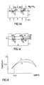
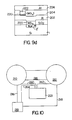
- Figs. 1a-1e are cross-sectional diagrams of a silicon wafer undergoing a refractory metal deposition process in accordance with a preferred embodiment of the invention.
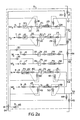
- Fig. 2a shows the components within a gas distribution box used in the preferred embodiment of the invention.
- Fig. 2b shows the gas distribution box of Fig. 2a along with heating elements used for baking components within the distribution box.
- Fig. 3 shows a CVD chamber used in the preferred embodiment of the invention.
- Fig. 4 is a graph showing emissivity vs. temperature of N and P type silicon regions.
- Fig. 5 is a graph showing the Si/W ratio of a deposited layer vs. the SiH4/WF6 process gas ratio.
- Fig. 6 is a graph showing deposition rate vs. SiH4/WF6 ratio.
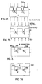
- Figs. 7a-7e are cross-sectional diagrams of a silicon wafer undergoing a blanket deposition process in accordance with a preferred embodiment of the invention.
- Fig. 8 is a cross-sectional diagram of a silicon wafer after completion of a process for forming a via between a polysilicon layer and a metal layer in accordance with a preferred embodiment of the invention.
- Figs. 9a-9d are cross-sectional diagrams of a silicon wafer after completion of a process for forming a via between two metal layers in accordance with a preferred embodiment of the invention.
- Fig. 10 shows a preferred embodiment structure for carrying out a via formation process.
- Fig. 11 shows the gas distribution network for sputter etch gases.
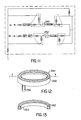
- Figs. 12 and 13 show perspective views of a gas diffusing means used in the preferred embodiment of the invention.
- a silicon wafer is processed using well known and conventional methods to form various regions in the silicon substrate for electrical contact thereto by an aluminum interconnection layer.
- a layer of silicon dioxide or other insulating layer is then formed over the surface of the wafer and etched using well known techniques to selectively expose regions of the silicon substrate for electrical contact of these exposed regions with the metal layer.
- An illustrative process for forming exposed silicon regions is described in U.S. Patent 4,546,370, incorporated herein by reference.
- step 1 of the preferred process to selectively form a barrier layer over the exposed silicon regions the wafer is subjected to a 120°C sulfuric peroxide acid bath for approximately five minutes to remove organic and metallic contamination from the exposed substrate surface. Any of the well known and conventional techniques for removing contaminants may also be used for this step. This step may be omitted if the contamination of the exposed substrate surface is deemed to be insignificant.
- step 2 the wafer is subjected to a buffered oxide etchant, such as that comprising five parts ammonium fluoride, one part hydrofluoric acid, and eight parts water, for approximately six seconds at room temperature.
- a buffered oxide etchant such as that comprising five parts ammonium fluoride, one part hydrofluoric acid, and eight parts water.
- This step removes native and other oxides from the exposed substrate surface. This step may be omitted if the exposed surface is deemed to be sufficiently free of oxide. Any number of other conventional and well known techniques for accomplishing this step may be also used.
- This oxide removal step also removes a portion of the surface of the patterned oxide; however, since this patterned oxide is relatively thick, this reduction in its thickness is negligible.
- any damage to the exposed silicon surface caused by any ion implantation or etching process is removed by a conventional nitrogen trifluoride (NF3) silicon etch or any other conventional and well known etching technique which would accomplish this step.
- NF3 etchant actually removes a top layer of the silicon where the damage to the crystal structure occurs.
- the silicon crystal lattice damage is preferably removed so that the refractory metal will nucleate rapidly with the silicon surface and in a predictable manner. This step may be omitted if the damage to the crystal lattice structure is not significant.
- a rapid thermal anneal may be performed to realign the silicon atoms and reform the crystal lattice structure. This anneal step is preferably conducted at between approximately 600°C-850°C for ten to sixty seconds depending on the type and amount of damage to be repaired.
- FIG. 1a A representative wafer having undergone steps 1-3 is shown in Fig. 1a. Silicon wafer 1 is shown having exposed N type region 2 and P type region 3, and having patterned oxide layer 4. Wafer 1 is then placed in a CVD chamber such as that shown in Fig. 3 and described in U.S. Patent No. 4,796,562, incorporated herein by reference. The CVD chamber of Fig. 3 will be described later.
- step 4 to ensure gas purity and stability, the process gases are purged through a bypass-to-waste vacuum line for at least seven seconds before the gas is allowed to be routed into the CVD process chamber containing wafer 1. To achieve the highest gas purity, this step 4 is conducted after each completed deposition process; however, this step may be omitted depending on the purity level tolerable and the desired accuracy of the flow rates.
- Fig. 2a is a schematic diagram of the gas routing, filtering, and purification network 5 used in the preferred embodiment CVD system.
- high purity (e.g., at least 99.999% pure) process gases SiH4, H2, Ar, and WF6 are supplied to input ports 6, 7, 8, and 9, respectively, of network 5 as shown.
- CVD chamber etchant gases SF6 and NF3 are supplied to input ports 10 and 11, respectively.
- all gas lines used are electropolished stainless steel.
- process gas valves 12-15, 22, 24, 26, 27, 40, 41, 47, and 48 are closed to isolate process gas lines 25, 30, 46, and 51.
- Etchant gas valves 16, 17, 34 and 38 are closed, as well as N2 valve 32, since these lines do not need to be purged of impurities.
- nitrogen backfill valves 55 and 56 are closed, as the backfill is used solely for dilution of the toxic and/or pyrophoric gases, and for diagnostic purposes, during maintenance. All other valves are open to pressurize the process gas lines with N2 to prevent contaminants from entering the lines.
- valves 18-21 and 23 are opened to allow N2 to pressurize SiH4 gas line 25.
- Valves 28 and 29 are opened to allow N2 to pressurize H2 gas line 30.
- Valves 31 and 42-45 are opened to allow N2 to pressurize Ar gas line 46.
- Valves 49 and 50 are opened to allow N2 to pressurize WF6 gas line 51.
- Gas lines 52, 53, and 54 connect to gas lines leading into a CVD chamber and are isolated from network 5 by the closure of the appropriate valves as discussed above.
- the various mass flow controllers (MFCs) 76, 77, 80, and 81 are of the high bypass type, such as the STEC model 3400SL-SP-UC bakeable MFC, available from STEC Corporation of Japan.
- the valves within dashed lines are of a monoblock design and are high precision valves, such as Motoyama model MVILM00BB, available from Motoyama Corporation of Japan.
- valves 19, 20, and 28 are closed to cut off the supply of N2 to gas lines 25 and 30.
- valves 12, 13, 22 and 26 are opened to allow the SiH4 and H2 gases to flow through lines 25 and 30 and through vacuum line 57.
- the flow rate of the SiH4 and H2 is determined by the pressure created by a pump (not shown) connected to vacuum line 57 and the extent of opening of MFC's 76 and 77.
- the flow rate of all the gases during this purging step is equal to the flow rates to be used during the refractory metal deposition process so that there will be no surging of the process gases when the gases are allowed to enter gas line 52.
- valves 42, 44, and 49 are closed to cut off the supply of N2 to gas lines 46 and 51.
- valves 14, 15, 40 and 47 are opened to allow the Ar and WF6 gases to flow through lines 46 and 51 and through vacuum line 58.
- the flow rates of the Ar and WF6 are determined by the pressure created by a pump (not shown) connected to vacuum line 58 and the extent of opening of MFC's 80 and 81 and are set to be equal to the flow rates to be used during the refractory metal deposition process.
- This purging of the gas lines is to be maintained for at least seven seconds to ensure high purity and flow rate stability.
- Process gases may now be controlled to enter the CVD process chamber via gas lines 52 or 54 by controlling valves 23, 24, 27, 29, 41, 43, 48, and 50 connected between vacuum lines 57 and 58, process gas lines 25, 30, 46, and 51, and CVD gas lines 52 and 54.
- the SiH4 reducing gas entering input port 6, the H2 gas entering input port 7, and the Ar gas entering input port 8 are filtered by appropriate NanochemTM filters 60, 61, and 62, respectively, which contain an organometallic compound, and again filtered by conventional porous type gas filters 70, 71, and 72, respectively.
- NanochemTM filters are manufactured by Semi-Gas, Inc., San Jose, California.
- the Ar gas is additionally filtered by Saes-PurifierTM filter 73, model St707, containing gettering material Zr-V-Fe.
- Etchant gases SF6 and NF3 are filtered by conventional porous type filters 74 and 75, respectively.
- the flow of the gases in lines 25, 30, 35, 39, 46, and 51 is controlled and measured by mass flow controllers (MFC) 76-81, respectively.
- MFC mass flow controllers
- Dew point sensors are placed in vacuum lines 57 and 58, and in N2 lines 84 and 85, to detect whether the H2O vapor content in these lines is below a predetermined level.
- gas routing and filtering network 5 Prior to being used as part of a CVD system, gas routing and filtering network 5 is baked at approximately 125°C for approximately 37 hours to bake out the water vapor in the gas lines.
- resistive heating elements 87 are contained within the network 5 enclosure for this purpose.
- the components 88 comprising network 5 are mounted on an aluminum substrate 89, and resistive heating elements 87 are mounted on the other side of the substrate 89 for heating the substrate and baking components 88.
- Residual gas analyzers are used to detect impurities in the gas lines.
- gases SiH4, H2, Ar, and WF6 may be substituted for the gases used in the preferred process described herein.
- a refractory metal based gas is allowed to enter the CVD process chamber containing wafer 1 to saturate the exposed silicon regions 2 and 3 at room temperature (e.g., less than 30°C) before any reducing gas is pumped into the chamber.
- WF6 is used to saturate the silicon substrate surface.
- any well known refractory metal based gas which can be reduced by silicon to deposit a refractory metal layer may also be used. This saturation step results in the WF6 being reduced by the exposed silicon so as to form a few monolayers of tungsten 90 on the exposed silicon regions 2 and 3.
- the WF6 is reduced by the exposed silicon in accordance with the following reaction: 2WF6+ 3Si ⁇ 2W + 3SiF4 (eq. 1)
- the fluorine atoms from the WF6 are removed as a volatile reaction product (SiF4), and tungsten is deposited on the surface of the silicon.
- SiF4 volatile reaction product
- the reaction of the Si surface with the WF6 may not be sufficient to form a refractory metal layer which covers the entire surface of the exposed silicon.
- This base layer of tungsten bonds strongly with the exposed silicon and, thus, increases the bonding strength of the subsequently formed barrier layer with the silicon substrate.
- This base layer also acts as a catalyst for the deposition of additional tungsten to promote the selective deposition of the refractory metal on essentially only the silicon and not on the SiO2 insulating layer 4.
- a layer of tungsten is not formed on SiO2 layer 4, since the SiO2 will not significantly reduce the WF6 at room temperatures.
- step 5 is conducted by controlling process gas valves 27, 41 and 48 of Fig. 2 to control the flow of H2, Ar, and WF6 entering the CVD chamber.
- Table I shows process parameters for the various steps used in the preferred embodiment process for selectively depositing a refractory metal layer. Step 5 corresponds to parameter setting A in Table I.
- this step is conducted for approximately 7 seconds at a WF6 flow rate of 4.0 sccm (standard cubic centimeters per minute) and a CVD chamber pressure of 80 mtorr.
- H2 is also injected into the chamber at a rate of 150 sccm by opening valve 27. H2 does not act as a reducing gas at this low temperature and, thus, acts as an inert gas.
- a small amount of Ar gas is also injected into the chamber at a rate of 5 sccm by opening valve 41. The Ar gas is used as a carrier gas to facilitate the flow of WF6 in gas line 54.
- Fig. 3 is a cross-sectional diagram of the chamber portion of a modified Varian Model 5101 CVD system used in the preferred embodiment process.
- the Varian Model 5101 CVD system is described in U.S. Patent No. 4,796,562, incorporated herein by reference.
- wafer 1 is shown held in place by wafer clamp assembly 100, securing wafer 1 to quartz chuck 102, and having a front surface facing reaction chamber 104.
- the refractory metal based gas e.g., WF6
- WF6 refractory metal based gas
- outer gas injector ring 108 where ring 108 allows the gas to exit through a diffusing means forming a portion of the wall of ring 108.
- a novel diffusing means is used in the preferred embodiment process and will be described in detail later with reference to Figs. 11-12.
- the gas enters ring 108 through an inlet port (not shown), which is connected to gas line 54 in Fig. 2.
- Ar gas also flows through gas line 54.
- Inner gas injector ring 110 is similar to ring 108 and is connected to gas line 52 in Fig. 2 for the injection of the reducing gas (e.g., SiH4) and H2 into chamber 104.
- Gas deflector 105 acts to help mix the gases injected into gas mixing chamber 106 prior to the gases entering into reaction chamber 104.
- backside chamber 114 is made to have a pressure of 0.5 torr by injecting Ar gas into backside chamber 114 via an inlet port (not shown).
- a pressure transducer (not shown) located in backside chamber 114 is used to measure the pressure in backside chamber 114.
- the precise value of the relatively high backside chamber pressure is not significant as long as the pressure is sufficient to prevent process gases in reaction chamber 104 from entering backside chamber 114 and nucleating with the back surface of silicon wafer 1.
- the backside pressure should not exceed approximately 1.0 torr because loss of selectivity around the water edge may occur.
- reaction chamber pressure is maintained at 80 mtorr.
- reaction chamber 104 The gases in reaction chamber 104 are withdrawn via high conductance vacuum port 116 through openings in wafer clamp assembly 100 so as to keep the residence time of any byproducts in chamber 104 below 10 milliseconds.
- the rate of withdrawal of the gases in chamber 104 keeps the process gases flowing at the desired rate and maintains the desired reaction chamber pressure.
- step 6 the temperature of the wafer is slowly increased above room temperature by a directed radiation source while injecting the refractory metal based gas (e.g., WF6) into the reaction chamber so that the refractory metal deposition rate on the silicon is very low.
- a directed radiation source e.g., WF6
- the refractory metal based gas is reduced by the exposed silicon on the surfaces of N type region 2 and P type region 3 in Fig. 1c and reduced by the silicon which diffused through the base layer of refractory metal deposited in step 5.
- the refractory metal 120 is deposited over both N and P type silicon regions 2 and 3 on tungsten 90 at essentially equal rates, since the emissivities of N and P type silicon at temperatures below 100°C are essentially equal.
- the temperature ramp must be slow enough to provide a resulting deposition of at least an optically opaque layer (e.g., 100-500 ⁇ ) of refractory metal 120/90 on both N and P type silicon regions 2 and 3 before the substrate temperature reaches approximately 100°C.
- the layer only need be opaque to the frequencies outputted by the radiant heating means used in the CVD chamber.
- Fig. 1c shows radiation 122 irradiating back substrate surface 124 of wafer 1, while opaque refractory metal layer 120 forms over N type region 2 and P type region 3.
- WF6 the refractory metal based gas
- the reduction reaction consumes a few atomic thickness layers of the silicon substrate during the deposition of the opaque layer of tungsten over the exposed silicon regions. Since there is essentially no reduction of the refractory metal based gas with the silicon dioxide insulating layer 4 at this low temperature, there is essentially no deposition of refractory metal on the silicon dioxide layer 4.
- this step 6 (parameter settings B and C in Table I) is carried out by providing ramped power to quartz halogen lamp 126, shown in Fig. 3, while WF6 is being injected into chamber 104 at a rate of 4 sccm. As shown in parameter settings B and C in Table I, lamp 126 remains off for five seconds, then is ramped up to 260°C over a period of 45 seconds. The flow rates of H2 and Ar, as well as the chamber pressure and backside chamber pressure, remain the same as in step 5.
- Pyrometer 128, shown in Fig. 3, is used to measure the average temperature of the wafer and provides feedback for temperature control.
- silicon tetrahydride (SiH4) reducing gas also known as silane
- SiH4 reducing gas is injected into chamber 104 at a flow rate of 2.6 sccm to help reduce the WF6 so as to increase the deposition rate of the refractory metal and to ensure very little of the silicon surface is consumed by the reduction process.
- the deposition temperature is held between 230°C and 425°C for a time to deposit a desired thickness of tungsten or other refractory metal on the selected areas of the silicon wafer.
- the refractory metal based gas is injected into the chamber along with a reducing gas to reduce the refractory metal based gas, since the silicon from the substrate is no longer able to diffuse through the deposited metal layer to reduce the refractory metal based gas.
- the refractory metal based gas is WF6 and the reducing gas is SiH4, which causes the following exothermic reactions, depending on the relative amount of SiH4 in the chamber:
- the reduction reactions shown in equations 2 and 3 occur in the following manner.
- the WF6 fluorinates the surface of the opaque tungsten layer deposited in step 6.
- SiH4 reacts readily on this fluorinated surface to deposit silicon and form volatile silicon fluorides (SiF4).
- the deposited layer of silicon then reacts with the WF6 gas molecules impinging on the silicon layer to produce the reduction reaction of equation 1.
- the reactions shown in equations 2 and 3 are actually the results of a series of sub-reactions, where in the WF6/SiH4 reduction reaction, tungsten film growth proceeds through cycles of tungsten/ silicon deposition. Since neither the WF6 or SiH4 significantly stick to the insulating silicon dioxide layer 4 at these relatively low deposition temperatures, there is essentially no deposition of tungsten on the insulating silicon dioxide layer and, thus, selective deposition of tungsten is obtained.
- the amounts of WF6 and SiH4 injected into the CVD reaction chamber are preferably set to deposit a layer of WSi x, where x depends on the process parameters.
- Fig. 5 is a graph showing the resulting Si/W ratio in a deposited layer at a deposition temperature of 320-380°C in response to varying the SiH4/WF6 ratio.
- the amount of SiH4 reducing gas provided to the CVD chamber is ramped to follow the increasing temperature of the contact area. Since the reduction reaction of the WF6 (or other refractory metal based gas) when combined with SiH4 is an exothermic reaction, as more tungsten is being deposited, the temperature of the deposited tungsten increases. As the temperature of the contact area increases, the ramped up supply of SiH4 increases the deposition rate of the refractory metal while the desirable columnar grain structure of the barrier layer is maintained due to the increased temperature at which the reaction occurs. Care must be taken to not supply too much SiH4 to the reaction prior to the temperature of the contact area rising to a certain level to maintain the columnar grain structure or else the grain structure of the resulting barrier layer will grow rapidly in an undesirable isotropic fashion.
- the deposited barrier layer 132 is formed to comprise between 5 and 20 atomic % Si (or between 1 and 4 weight % Si). Using the above-described process, the layer 132 comprises approximately 12 atomic % Si, although all that is needed is for the composition to exceed 5 atomic % Si to avoid reduction of the Si substrate.
- step 7 is carried out by ramping up quartz halogen lamp 126 over a 45 second period to achieve a measured wafer temperature of 260°C.
- SiH4 is injected into chamber 104 at a rate of 2.6 sccm by controlling valve 24.
- the remaining gas flows and pressures are identical to those used in process parameter setting B of Table I.
- the ramping of SiH4 depends on the extent of exposed silicon area of the wafer. In the above-described process, it is assumed less than 3% of the wafer surface comprises exposed Si. If more of the silicon is exposed, the SiH4 may be ramped up faster.
- step 8 the wafer is allowed to cool, the process gases are removed from the chamber, and a rapid thermal anneal step is used to silicide the refractory metal/silicon substrate interface and thereby lower the contact resistivity. Also, during this step, the silicon atoms within the barrier layer react with the deposited refractory metal to form a silicide. Since the reducing gas is silicon based, the deposited refractory metal already contains silicon, and the silicon substrate is not significantly consumed during this step. In the preferred embodiment, this anneal is accomplished at between approximately 650°C to 900°C for approximately 10-30 seconds.
- Table I in parameter settings I-K, shows the preferred cool-down and purging step conducted prior to annealing, where, in setting I, lamp 126 is turned off, the injection of process gases SiH4, H2, Ar, and WF6 into the chamber is ceased by closing the appropriate valves in Fig. 2, and the pressures in reaction chamber 104 and backside chamber 114 are reduced to less than 18 mtorr.
- H2 is allowed to enter reaction chamber 104 at a flow rate of 300 sccm
- Ar is allowed to enter reaction chamber 104 at a flow rate of 50 sccm, in order to promote cooling of the wafer and to purge gas lines 52 and 54 and reaction chamber 104 of any remaining SiH4 and WF6.
- the pressure in reaction chamber 104 is kept at 800 mtorr, while the backside chamber pressure is held at 1.0 torr.
- Setting J is held for approximately 45 seconds so that the wafer is sufficiently cooled and the lines and reaction chamber are sufficiently purged.
- parameter setting K the gases are removed from reaction chamber 104, and the pressures in reaction chamber 104 and backside chamber 114 are lowered to below 18 mtorr for five seconds.
- the anneal step is conducted during process parameter setting L, where lamp 126 is supplied ramped power to heat the wafer to approximately 700°C over a 20 second period.
- H2 is supplied to reaction chamber 104 at a rate of 150 sccm
- Ar is supplied to reaction chamber 104 at a rate of 5 sccm.
- the pressure in reaction chamber 104 is maintained at 80 mtorr, while the backside chamber 114 pressure is maintained at 0.5 mtorr.
- the deposited barrier layer densifies and shrinks approximately 10%. This shrinkage is primarily due to the tungsten bonding with the silicon within barrier layer 132. The amount of shrinkage depends on the anneal temperature and the Si content in barrier layer 132.
- the resulting barrier layer 132 formed during the preferred process steps 5-8 is approximately 6500 ⁇ thick.
- step 9 the wafer is cooled down after annealing to bring the substrate to a temperature below 100°C before removal from the CVD chamber.
- This cooling step is accomplished by turning off power to lamp 126 and allowing the wafer to cool for at least 45 seconds to approach ambient temperature.
- gases H2 and Ar may be injected into reaction chamber 104 at flow rates of 300 sccm and 50 sccm, respectively, for approximately 45 seconds while providing a reaction chamber pressure of 800 mtorr and a backside chamber pressure of 1.0 torr. The H2 and Ar gases are then shut off, and the wafer is removed from the reaction chamber.
- an aluminum deposition process or other applicable metal or polysilicon deposition process, is conducted, using conventional techniques, to form a conductive interconnect layer over the deposited barrier layer.
- aluminum is deposited for the interconnect layer using a sputter deposition process.
- the resulting structure is shown in Fig. 1e, where conductive layer (Al) 136 is shown overlying barrier layer 132.
- the pumping manifold to the CVD process chamber has a conductance of ⁇ 50 torr liters per second. Using a chamber pressure of 120 mtorr and a chamber volume of 49 liters, the residence time of the gas within the process chamber will be approximately 9.8 x 10 ⁇ 3 seconds.
- the process gases entering the CVD chamber should be kept to at least 99.999 designated purity, and critical gas flows should be controlled to within ⁇ 0.2 sccm of flow setpoint from wafer to wafer to achieve sufficient repeatability.
- the liquid gas container containing the WF6 (or other refractory metal based gas) is cooled to preferably 5°C below room temperature to prevent condensation of the gas in the gas lines.
- the above-described process for forming a barrier layer over regions of silicon may be used with other than the process gases specifically described with respect to the preferred embodiment.
- refractory metal based gases comprising refractory metals molybdenum, palladium, platinum, or tantalum may be used.
- a reducing gas other than that described in the preferred embodiment may also be used where appropriate.
- the gas flow rates, temperatures, process times, pressures, and apparatus limitations described with respect to the preferred embodiment process may be modified as necessary to form a barrier layer having the desired characteristics.
- a refractory metal is deposited on the exposed silicon regions as well as on the surface of the insulating silicon dioxide layer.
- the refractory metal layer deposited over the oxide layer is then completely etched away using a blanket etch so that the refractory metal remains only over the silicon regions to be electrically contacted by the refractory metal.
- a metallization layer is then typically formed over the surface of the wafer to contact the deposited refractory metal in order to electrically contact the underlying silicon regions.
- blanket deposition examples include depositing the refractory metal over a gate oxide layer and selectively etching the refractory metal layer to form gates for MOS devices.
- the preliminary steps 1-4 of cleaning the surface of the silicon wafer, removing any damage to the silicon crystal lattice, and purging the various gas lines are conducted as described above with respect to steps 1-4.
- step 5 of the preferred embodiment blanket deposition process after steps 1-4 are carried out and the wafer is placed in a CVD chamber such as that shown in Fig. 3, the wafer is then heated to a deposition temperature of approximately 500°C, and SiH4 is allowed to enter the chamber to nucleate with the exposed silicon and SiO2 for a period of approximately two seconds. This forms a few monolayers of SiH4 over the SiO2 to enable the subsequent reduction of WF6 when WF6 is later allowed to enter the chamber.
- Fig. 7a shows this step where radiant heat 150 supplied by lamp 126 in Fig. 3 heats wafer 1 during the injection of SiH4 into CVD chamber 104, causing a deposition of thin SiH4 layer 152 over the surface of wafer 1.
- step 6 a deposition process similar to that described with respect to step 7 of the selective deposition process, previously described, is conducted, where WF6 is injected into the CVD chamber along with SiH4. This step is conducted until a barrier layer composed of WSi x , where x depends on the ratio of SiH4 to WF6 used during the deposition process, having a desired thickness is formed over both the silicon and the oxide. The ratio of SiH4 to WF6 is reduced to below unity in order to achieve a columnar grain structure. This step is shown in Fig. 7b where deposited layer 158 is formed over the surface of the wafer 1.
- this deposition step is conducted generally using parameter settings D-H of Table I, where the quantity of reducing gas SiH4 is ramped up with time as the exothermic reduction reactions continually raise the temperature at the surface of the deposited barrier layer 158. In this step, however, the deposition temperature is maintained at approximately 500°C.
- Ramping should be ceased at the time when there is no further increase in barrier layer temperature due to the heat produced by the exothermic reduction reactions being more quickly removed as the barrier layer fills the contact regions.
- step 7 after the barrier layer 158 is deposited, the gas lines and the CVD process chamber are purged and the wafer is cooled similar to that described with respect to step 7 of the above-described process and parameter settings I-K in Table I.
- An anneal step is conducted at a temperature of between 650°C to 900°C for approximately 10-30 seconds with process parameter settings similar to that in parameter setting L of Table I.
- the resulting barrier layer 158 is then etched using one of any number of well known blanket plasma etching techniques, or other acceptable etching technique, so as to leave the deposited barrier layer 158 only within the contact areas, such as shown in Fig. 7c. In certain applications, this barrier layer 158 may be used as an interconnect layer and, thus, no blanket etch would be conducted.
- a metallization layer or other conductive layer 160 is then deposited and etched, as shown in Fig. 7d.
- Conductive layer 160 forms an ohmic contact with the deposited barrier layer 158 and with regions 2 and 3.
- Additional features to improve the quality of the deposited barrier layer are identical to those described with respect to the process described above, for selectively forming a refractory metal silicide layer.
- steps 1-9 of the selective deposition process or steps 1-7 of the blanket deposition process may generally be used to form vias between a polysilicon layer and a metal layer or between two metal layers.
- FIG. 8 A representative wafer having a via formed in accordance with the preferred method is shown in Fig. 8.
- wafer 1 includes N type region 2 and P type region 3.
- Polysilicon layer 170 is formed using conventional methods to contact regions 2 and 3.
- Oxide layer 4 insulates polysilicon layer 170 from the silicon wafer 1.
- Insulating layer 172 is formed over polysilicon layer 170 to expose a contact portion of polysilicon layer 170, over which is deposited refractory metal via 174.
- refractory metal via 174 comprises WSi x , where x depends on the ratio of reducing gas SiH4 to WF6 used in the deposition process.
- a metal layer 178 such as comprising AlSi, is then formed over insulating layer 172 to contact via 174 and to provide an electrical connection between metal layer 178 and polysilicon layer 170.
- Step 3 of the previously described process for removing any damage to the crystal lattice structure of the substrate is, of course, deleted.
- step 6 In a selective deposition process to form a via, although there are no problems with different emissivities of N and P regions in the polysilicon layer, it is still desirable to conduct step 6 to deposit a thin layer of refractory metal on the polysilicon prior to injecting SiH4 into the CVD chamber to achieve a stronger bond between the via and the polysilicon and to ensure selectivity. A thin layer of the polysilicon will be consumed.
- the remaining deposition and anneal steps for the selective deposition process are basically identical to those previously described for forming a conductive barrier layer between regions in a substrate and a metal layer.
- process times, gas flow rates, and temperatures may be changed to achieve the desired characteristics of the deposited refractory metal via.
- SiH4 is first injected into the chamber at a deposition temperature of approximately 500°C for approximately 2 seconds to form a thin SiH4 layer over the surface of the wafer. This method is similar to that discussed with respect to Fig. 7a. WF6, along with SiH4, is then introduced to form a barrier layer similar to that described with respect to Fig. 7b. The deposited layer is etched, and a metallization process is conducted similar to the method discussed with respect to Figs. 7c and 7d.
- the aluminum layers To form a via between two aluminum layers, or between any two metal layers, it is desirable to form the aluminum layers to contain silicon atoms to prevent the Al atoms from reacting with the oxide surface of the wafer.
- a patterned layer of oxide 201 or other insulating material is formed over the aluminum layer, using conventional techniques, to expose contact regions.
- This starting structure is shown in Fig. 9a.
- Fig. 9a shows wafer 1 having P or N type region 2' formed therein and contacted by refractory metal barrier layer 200, formed by methods previously described herein.
- Over barrier layer 200 is formed aluminum layer 202, over which is formed patterned oxide layer 204. The following preferred process is then implemented.
- step 1 to selectively deposit a barrier layer over aluminum layer 202, the exposed aluminum is cleaned by, preferably, using a conventional RF sputter etch process.
- Ar ions are used in the sputter etch using a bias voltage of -600 volts or less.
- a Varian Model 5101 CVD system is modified to have a sputter etch station connected thereto, as shown in Fig. 10.
- the Varian 5101 CVD chamber has been previously described with respect to Fig. 3 and is described in U.S. Patent 4,796,562.
- CVD chamber 210 is connected to sputter etch chamber 212 via a wafer transport system 214.
- Load locks (not shown) between wafer transport system 214 and chambers 210 and 212 are used so that the pressure in chamber 210 is not affected by the pressure in chamber 212 while wafer transport system 214 is not being used.
- gas lines 216 and 218 are connected to CVD chamber 210 and sputter etch chamber 212, which is described with respect to Fig. 2.
- the Ar gas supplied to sputter etch chamber 212 via gas line 218 is controlled by the valve arrangement shown in Fig. 11, which is located within gas box 219 and adjacent network 5 shown in Fig. 2a.
- the various filters, MFC, and valves associated with Ar gas line 250 are similar to those corresponding components connected to Ar gas line 46 in Fig. 2a.
- a krypton gas source is shown connected to Kr gas line 252. This Kr source and associated valves are not used in the preferred sputter etch process.
- Automated control system 221 controls the various functions of CVD chamber 210, sputter etch chamber 212, wafer transport system 214 and gas box 219 by sending the appropriate signals on wires 260, 262, and 264, respectively.
- the wafer of Fig. 9a is placed in a cassette tray and the cassette tray is placed into a cassette chamber within wafer transport system 214.
- Wafer transport system 214 is similar to that described in U.S. Patent 4,796,562.
- the wafer transport system 214 uses manipulator arms to place a wafer from the cassette tray into sputter etch chamber 212, which at a very low pressure (e.g., 1 x 10 ⁇ 4 torr).
- Sputter etch chamber 212 containing Ar gas is then operated for cleaning the surface of the wafer to remove any oxide from the surface of aluminum layer 202 and to remove any contaminants from the surface of the wafer which may adversely affect the selective deposition of the refractory metal on aluminum layer 202.
- This step also cleans the SiO2 surface to prevent any subsequent nucleation of WF6 or SiH4 process gases with the SiO2 surface.
- a sputter etch using a bias voltage of preferably -580 volts and 400 watts of RF power is conducted at room temperature for approximately 60 seconds at a pressure of 14 mtorr and an Ar gas flow rate of 48.5 sccm.
- wafer transport system 214 and sputter etch chamber 212 are pulled down to a pressure of approximately 1 x 10 ⁇ 4 torr.
- the load lock between sputter etch chamber 212 and wafer transport system 214 is then opened so that the wafer may be transported via a manipulator arm out of sputter etch chamber 212.
- the load lock between wafer transport system 214 and sputter etch chamber 212 is closed and the load lock between wafer transport system 214 and CVD chamber 210 is opened so that the manipulator arm can place the etched wafer into position within CVD chamber 210 without the wafer becoming contaminated.
- step 2 the wafer undergoes a saturation step in step 2 wherein a refractory metal based gas is injected into the CVD chamber at room temperature (e.g., less than 30°C) for a short period.
- step 2 shown as parameter setting A in Table II, is conducted for seven seconds with a WF6 flow rate of 4.0 sccm, a H2 flow rate of 150 sccm, and an Ar flow rate of 5 sccm.
- reaction chamber 104 is made to have a pressure of 50 mtorr and backside chamber 114 is made to have a pressure of 0.5 torr. This step is used to improve bonding between the subsequently formed via and the metal layer.
- step 3 shown in Table II as parameter settings B-D, the temperature of the wafer is raised to approximately 450°C for 120 seconds, and the refractory metal based gas is injected into the chamber along with H2 and Ar, at the same flow rates as in parameter setting A.
- the patterned oxide layer overlying the aluminum layer does not cause a reduction reaction to occur when contacted by WF6.
- the H2 is able to reduce the refractory metal based gas at the surface of the aluminum layer in accordance with the following equation: WF6 + 3H2 ⁇ W + 6HF (eq. 6)
- the temperature of the wafer is ramped down to ambient temperature and the pressure inside the CVD chamber is increased.
- the gases in the chamber are purged.
- the appropriate valves, shown in Fig. 2 are operated to inject the desired flow rate of process gases into the CVD chamber.
- refractory layer 220 is deposited on aluminum layer 202.
- step 4 shown as parameter setting F, SiH4 is injected into the CVD chamber for about five seconds prior to the wafer being ramped up in temperature. SiH4 is used to obtain a high deposition rate of the refractory metal over the exposed aluminum layer.
- step 4 the temperature of the wafer is ramped up to approximately 500°C over a period of 45 seconds and maintained at this temperature for 50 seconds.
- the supply of SiH4 is ramped up from 2.6 sccm to 3.4 sccm so as to increase the deposition rate of the refractory metal as the temperature of the deposited refractory metal layer increases due to the exothermic reduction reactions.
- the columnar grain structure of the deposited refractory metal is preserved due to the increased temperature of the deposited refractory metal from the exothermic reduction reactions.
- deposited refractory metal (WSi x ) layer 222 is deposited over refractory metal (W) layer 220.
- step 5 corresponding to parameter settings M-O, the wafer is cooled by ramping down power to lamp 126 in Fig. 3 as the gases in the CVD chamber are evacuated.
- parameter setting N the temperature of the wafer is further ramped down to ambient temperature over a period of 45 seconds by lowering the power applied to lamp 126 in Fig. 3.
- H2 and Ar are injected into the CVD chamber to achieve a pressure in CVD chamber 104 of 800 mtorr and a pressure in backside chamber 114 of 1.0 torr.
- the process gases are again removed as shown in parameter setting O.
- the CVD chamber is pumped out, and the load lock between wafer transport system 214 and CVD chamber 210 is opened.
- the manipulator arm removes the wafer from CVD chamber 210 and places it into a cassette within wafer transport system 214 in a manner similar to that described in U.S. Patent No. 4,796,562.
- N2 is injected into wafer transport system 214 to pressurize system 214 to slightly higher than atmospheric pressure.
- the cassette containing the wafer (and containing other wafers in the lot) is then removed.
- the above-described process forms a via of approximately one micron in thickness.
- An aluminum layer 224 is then formed over the surface of the wafer, as shown in Fig. 9d, using conventional techniques.
- Deposited refractory metal 222 now forms a via between aluminum layers 202 and 224.
- the wafer is initially placed in CVD chamber 210 in Fig. 10 via wafer transport system 214.
- SiH4 is injected into CVD chamber 210 at a deposition temperature of between 265°C and 500°C for two seconds to promote blanket deposition on the aluminum as well as the oxide surface.
- the refractory metal barrier layer is deposited to the desired thickness
- the refractory metal is etched so as to leave only a via having a desired thickness.
- An upper metal layer is then formed, using conventional techniques, over the wafer surface.
- the resulting structure is similar to that shown in Fig. 9d, except pure refractory metal layer 220 is not formed during this blanket deposition process.
- the residence time of reaction by-products should be kept below 10 milliseconds, the reactive gases should be kept to at least 99.999 designated purity, and critical gas flows should be controlled to within ⁇ 0.2 sccm.
- portions of the CVD chamber such as quartz chuck 102 in Fig. 3, will become coated with a layer of refractory metal and undesirably absorb radiation and react with the gases in the process chamber.
- an etch gas of NF3 is injected into the chamber by, for example, opening valves 17, 37, and 38 in Fig. 2.
- this etch step is conducted while the CVD chamber is at room temperature.
- a drawback of this prior art method is that the NF3 reacts with the quartz (SiO2) in the chamber, and with any reaction by-products remaining in the chamber, and forms a condensation of SiF4 or other fluorides.
- reaction chamber walls are heated to above 65°C by, for example, a closed loop heating unit such as that manufactured by Mydax, while maintaining a chamber pressure of less than approximately 80 mtorr during etching the chamber with NF3. Any condensation is avoided in this novel process, since at this temperature, the SiF4 or other formed fluoride is volatile and is purged away with the NF3.
- a closed loop heating unit such as that manufactured by Mydax
- Table III below shows a preferred process for conducting this NF3 etch of the CVD chamber, such as CVD chamber 104 in Fig. 3.
- step A of Table III 50sccm of NF3 is injected into CVD chamber 104 of Fig. 3 at a low pressure (at or below 80 mtorr). Two hundred watts of RF power is then applied for a period of approximately five minutes, while the quartz walls of the CVD chamber are kept at approximately 90°C. No backside gas is used to pressurize backside chamber 114 in Fig. 3.
- step B the RF power is turned off and the NF3 gas is withdrawn from the chamber.
- step C 175sccm of H2 is injected into the CVD chamber, and RF power of 200 watts is again applied for five minutes to clean up residue in the chamber.
- step D the chamber is again evacuated.
- step E 350sccm of H2 is injected into the CVD chamber at a chamber pressure of 800 mtorr for five minutes to flush out impurities from the etching process.
- step F the chamber is again evacuated.
- the CVD chamber has now been cleaned and is ready for further deposition processes.
- gas ejector rings in the CVD chamber such as rings 108 and 110 in Fig. 3, having an improved gas diffusing means so as to evenly diffuse the gas exiting the rings into the CVD chamber.
- gas ejector ring 260 has fitted on its upper portion a diffusing means 262 composed of grains of stainless steel, or grains of an equivalent inert material, sintered together to randomly direct the gas escaping through spaces between the sintered grains.
- the average size of the powder grains is in the range of 0.5 to 2.0 microns.
- the thickness of diffusing means 262 is 0.062 in., while the diameter of diffusing means 262 is approximately 7 in.
- diffusing means 262 and ring 264 may be any size as appropriate for the specific application.
- Non-porous support ring 264 is preferably composed of stainless steel.
- the diffusing means may be formed by cutting to a desired shape a prefabricated sheet of sintered stainless steel powder, available from Mott Metallurgical Corporation, Farmington, Conn.
- the ring-shaped diffusing means 262 is then welded to non-porous support ring 264.
- An inlet port 266 allows gas to enter gas ejector ring 262.
- the various gas flows and other process parameters are performed automatically under control of a computer, shown as automated control system 221 in Fig. 10.
- automated control system 221 in Fig. 10.
- human error is avoided by the automation of the various processes described above.
- One of ordinary skill in the art may easily develop a software program and control system to automate a process which will result in the desired characteristics of the deposited refractory metal layer.
- the software used in the preferred embodiment further controls the gas line purge function, described with respect to step 4 in the selective deposition process, previously described.
Abstract
Description
- This invention relates to integrated circuits implemented in silicon, and in particular to an improved process for providing electrical contact to silicon using a refractory metal.
- In providing electrical connections to silicon for microelectronics applications, it is frequently desired to provide a conductive interface between a metallization layer, such as aluminum (Al), and the portion of silicon to be electrically connected to the aluminum to prevent direct contact of the aluminum with the silicon. If aluminum were to be directly deposited onto the silicon, various problems may arise.
- One significant problem in depositing aluminum directly on silicon is that the aluminum acts as a P-type dopant, and any migration of aluminum atoms into a silicon region would dope the silicon region with P-type impurities. This is especially significant when the aluminum contacts an N-type silicon region, where the migration of P-type aluminum atoms into the silicon region results in an undesired rectifying contact.
- Another problem is that the aluminum is prone to spiking through shallow silicon regions, thus causing the aluminum to contact the underlying or adjacent silicon region.
- A further problem relates to the shadowing effect, where an oxide layer is etched to expose a silicon region, and the relatively high step between the top surface of the oxide and the exposed silicon results in uneven deposition of aluminum on the exposed silicon surface and on the oxide walls. This may even result in an open circuit due to insufficient aluminum being deposited on the exposed silicon or oxide walls.
- With decreasing geometries, the above problems become more acute. Further, increased reaction temperatures exacerbate the above-mentioned problems, since the migration of aluminum atoms into the silicon is accelerated with increasing temperatures. Additionally, over a period of time, the aluminum atoms further migrate into the silicon causing latent defects and low reliability contacts.
- Various schemes are used in the prior art to avoid the above-mentioned problems incurred by direct contact of aluminum with silicon. One way to overcome the above-mentioned problems is to saturate the aluminum during deposition with silicon (typically 0.2-1 weight % of Si to Al) to inhibit migration of the aluminum atoms. One drawback with this method is that the saturation level of aluminum is higher at higher temperatures so that when the saturated aluminum cools, a precipitate of silicon exists at the surface of the silicon substrate under the aluminum layer, resulting in an undesired P-type epitaxial layer. Additionally, the problem of shadowing effect still exists using the above method.
- Another prior art method used to avoid the problems resulting from direct contact of aluminum with silicon is to form one or more interface layers over the silicon before depositing the aluminum metallization layer. This type of process is generally described in U.S. Patent 3,777,364 to Schinella et al., although numerous other patents describe similar processes. In this prior art method, a refractory metal, such as tungsten, molybdenum, palladium, platinum, or tantalum, is deposited and reacted with the exposed silicon (or a polysilicon layer) to form a silicide layer. The top portion of the deposited refractory metal, which has not reacted with the silicon, may then be removed. The aluminum metallization layer is then deposited. The resulting silicide layer between the aluminum and silicon acts as a barrier to the aluminum atoms, preventing migration of the aluminum into the silicon, and provides a low resistivity contact between the aluminum and the silicon. Additionally, this type of process slightly reduces the step height (e.g., by 1200Å) during deposition of the aluminum metal layer.
- A problem with the above teaching of forming a silicide layer is that, when forming, for example, tungsten silicide as the interface layer between aluminum and silicon using a chemical vapor deposition (CVD) process and tungsten hexafluoride (WF₆) as the reactant gas, the high temperatures involved in the CVD process cause the hot CVD chamber walls to react with the WF₆ gas. This results in a lowering of the deposition rate of the tungsten onto the surface of the wafer.
- Although sputtering tungsten onto the surface of the wafer does not incur the problem of hot walls of a chamber reacting with the metallic fluoride gas, sputtering refractory metal films is subject to the following limitations: (1) such films are frequently highly stressed and crack; (2) such films are characterized by relatively poor step coverage; (3) such films are relatively costly to produce; (4) only a relatively small number of wafers can be processed in a given amount of time; and (5) sputtering equipment is relatively expensive to purchase and operate.
- Thus, using a hot-wall CVD process to deposit a refractory metal onto the silicon results in the deposition rate being limited, and the problem with step height is not avoided to the extent desirable.
- U.S. Patent No. 4,794,019 to Miller describes a tungsten deposition process using a hot-wall CVD chamber and mentions that the deposition rate of the tungsten decreases with time to reach a stable value of 25 Å/min at a thickness of about 3000 Å (col. 3, lines 31-33). Miller teaches a CVD process temperature on the order of 300°C to deposit the tungsten on the surface of the silicon wafer. Since tungsten nucleates well to silicon but not to SiO₂ at this temperature, this process is used to selectively deposit the tungsten on the silicon and not on SiO₂. By using this method, however, an increase in the thickness of the refractory metal over approximately 3000 Å is relatively time consuming and expensive.
- One way used to solve the problem of low deposition rates due to the hot walls of a chamber reacting with the metallic fluoride gas is to heat the wafers locally using direct irradiation of the wafer by means of a quartz halogen lamp or some other source of radiation. This method of heating the wafer, however, results in different refractory metal deposition rates on N and P type silicon regions due to the different emissivities of these two regions when heated by a radiation source. This uneven deposition increases the difficulty of efficiently depositing a metal interconnect layer providing good electrical contact to both the N and P type silicon regions.
- What would be desirable in the industry is a method of depositing a refractory metal as a barrier layer between aluminum and silicon at a relatively high deposition rate so as to reduce step height to a desirable amount, and which would result in an even deposition of refractory metal over both exposed N and P type silicon regions.
- The present inventive process relates to the deposition of a refractory metal onto a silicon surface for use in the manufacture of microelectronic circuits. In one embodiment, the deposition is a controllable selective deposition.
- To avoid the various problems discussed previously, a cold wall radiantly heated chemical vapor deposition (CVD) system is preferably used to deposit the refractory metal, wherein each wafer is heated by, for example, a broad band light source. Thus, the deposition of the refractory metal onto the wafer to form a barrier layer between the silicon substrate and an aluminum layer will not be limited by any reaction of the process gases (e.g., WF₆) with high temperature chamber walls.
- In a preferred embodiment, to avoid the varying deposition rates on N and P type silicon regions due to the different emissivities of these two regions when subjected to radiation, an optically opaque layer (e.g., at least 100-500Å) of the refractory metal is first formed on both the N and P type silicon regions prior to the N and P type regions reaching a temperature of approximately 100°C. The opaque layer is desirable to form at below 100°C, since at above 100°C, the emissivities of the N and P type regions begin to widely diverge. Once the opaque refractory metal layer has been established, the emissivities of both the N and P type regions at the higher processing temperatures will be approximately that of the refractory metal, thereby establishing an approximately equivalent deposition rate on both N and P type silicon regions.
- Additionally, at the higher deposition temperatures (e.g., 200-300°C), in the preferred embodiment, the amount of reducing gas (e.g., SiH₄ ) introduced into the CVD chamber to reduce the refractory metal gas (e.g., WF₆) is ramped up with time so that, as the thickness of the deposited refractory metal increases and the temperature of the contact area increases due to the exothermic reduction reactions, more reducing gas is made available in the CVD chamber to increase the deposition rate of the refractory metal.
- The various steps used in the preferred process for forming a silicide barrier layer comprise: (1) cleaning the exposed surface of a silicon wafer to remove organic and metallic contamination from the silicon regions to be contacted; (2) cleaning the surface of the wafer to remove oxide from the silicon regions to be contacted; (3) removing any damage to the silicon crystal lattice structure so that the refractory metal will nucleate rapidly and in a predictable manner; (4) purging the various gas lines and process chamber to ensure high purity of the process gases and accurate flow rates; (5) saturating the silicon surface at approximately room temperature (e.g., 20-30°C) with a refractory metal gas to form an initial layer of refractory metal on the silicon surface to act as a catalyst for subsequent deposition of the refractory metal and to form a strong bond between the silicon surface and the subsequently formed barrier layer; (6) ramping the temperature of the wafer, while injecting process gases into the CVD chamber, at a slow enough rate to form an optically opaque layer (e.g., at least 100-500Å) of refractory metal on the exposed silicon regions prior to the temperature of the regions reaching approximately 100°C; (7) heating the wafer at a relatively constant deposition temperature while ramping up the supply of reducing gas to increase the deposition rate of refractory metal as the exothermic reduction reactions continue to increase the temperature of the deposited refractory metal layer; (8) annealing the wafer at a temperature above approximately 650°C to silicide the refractory metal/silicon surface interface and to react the silicon atoms within the deposited refractory metal to form a silicide in order to lower contact resistivity; and (9) cooling the wafer before removal from the CVD chamber.
- In the preferred embodiment of the novel process summarized above, a silicon-based reducing gas (e.g., SiH₄) is used in step 7 to reduce the refractory metal gas (e.g., WF₆) so that silicon atoms are deposited along with the refractory metal. Thus, when the refractory metal and silicon undergo the
thermal anneal step 8, the silicon substrate is not significantly consumed. - In addition to the previously described features providing the advantages of high deposition rate and equal deposition on N and P type regions, further novel features of the above described process include using a high conductance vacuum system to limit the residence time of any impurities in the chamber, using a novel diffusing means inside the CVD chamber for diffusing process gases as they enter the CVD chamber, and using an improved gas distribution and filtering system.
- An additional novel process step includes cleaning the CVD chamber, after completing a number of refractory metal deposition processes, by heating the CVD chamber to above approximately 65°C during in-situ NF₃ cleaning of the CVD chamber to avoid condensation of by-products on the walls of the chamber.
- Minor modifications of the deposition process summarized above enable the process to be used for blanket deposition of a refractory metal and for deposition of a refractory metal for use as a via between two conductive layers. A novel apparatus is also described for forming vias, which enables the transfer of wafers from a sputter etch station to a CVD chamber under low pressure.
- The invention is further described below, by way of example, with reference to the accompanying drawings, in which:
- Figs. 1a-1e are cross-sectional diagrams of a silicon wafer undergoing a refractory metal deposition process in accordance with a preferred embodiment of the invention.
- Fig. 2a shows the components within a gas distribution box used in the preferred embodiment of the invention.
- Fig. 2b shows the gas distribution box of Fig. 2a along with heating elements used for baking components within the distribution box.
- Fig. 3 shows a CVD chamber used in the preferred embodiment of the invention.
- Fig. 4 is a graph showing emissivity vs. temperature of N and P type silicon regions.
- Fig. 5 is a graph showing the Si/W ratio of a deposited layer vs. the SiH₄/WF₆ process gas ratio.
- Fig. 6 is a graph showing deposition rate vs. SiH₄/WF₆ ratio.
- Figs. 7a-7e are cross-sectional diagrams of a silicon wafer undergoing a blanket deposition process in accordance with a preferred embodiment of the invention.
- Fig. 8 is a cross-sectional diagram of a silicon wafer after completion of a process for forming a via between a polysilicon layer and a metal layer in accordance with a preferred embodiment of the invention.
- Figs. 9a-9d are cross-sectional diagrams of a silicon wafer after completion of a process for forming a via between two metal layers in accordance with a preferred embodiment of the invention.
- Fig. 10 shows a preferred embodiment structure for carrying out a via formation process.
- Fig. 11 shows the gas distribution network for sputter etch gases.
- Figs. 12 and 13 show perspective views of a gas diffusing means used in the preferred embodiment of the invention.
- To selectively deposit a refractory metal on an exposed silicon surface for improved electrical contact between a metallization layer and the silicon, while achieving the advantages previously described, the below-described preferred process is used.
- Initially, a silicon wafer is processed using well known and conventional methods to form various regions in the silicon substrate for electrical contact thereto by an aluminum interconnection layer. A layer of silicon dioxide or other insulating layer is then formed over the surface of the wafer and etched using well known techniques to selectively expose regions of the silicon substrate for electrical contact of these exposed regions with the metal layer. An illustrative process for forming exposed silicon regions is described in U.S. Patent 4,546,370, incorporated herein by reference.
- In
step 1 of the preferred process to selectively form a barrier layer over the exposed silicon regions, the wafer is subjected to a 120°C sulfuric peroxide acid bath for approximately five minutes to remove organic and metallic contamination from the exposed substrate surface. Any of the well known and conventional techniques for removing contaminants may also be used for this step. This step may be omitted if the contamination of the exposed substrate surface is deemed to be insignificant. - In
step 2, the wafer is subjected to a buffered oxide etchant, such as that comprising five parts ammonium fluoride, one part hydrofluoric acid, and eight parts water, for approximately six seconds at room temperature. This step removes native and other oxides from the exposed substrate surface. This step may be omitted if the exposed surface is deemed to be sufficiently free of oxide. Any number of other conventional and well known techniques for accomplishing this step may be also used. This oxide removal step also removes a portion of the surface of the patterned oxide; however, since this patterned oxide is relatively thick, this reduction in its thickness is negligible. - In
step 3, any damage to the exposed silicon surface caused by any ion implantation or etching process is removed by a conventional nitrogen trifluoride (NF₃) silicon etch or any other conventional and well known etching technique which would accomplish this step. This particular process using an NF₃ etchant actually removes a top layer of the silicon where the damage to the crystal structure occurs. The silicon crystal lattice damage is preferably removed so that the refractory metal will nucleate rapidly with the silicon surface and in a predictable manner. This step may be omitted if the damage to the crystal lattice structure is not significant. - Instead of an etch of the silicon to remove any damage, a rapid thermal anneal may be performed to realign the silicon atoms and reform the crystal lattice structure. This anneal step is preferably conducted at between approximately 600°C-850°C for ten to sixty seconds depending on the type and amount of damage to be repaired.
- A representative wafer having undergone steps 1-3 is shown in Fig. 1a.
Silicon wafer 1 is shown having exposedN type region 2 andP type region 3, and having patternedoxide layer 4.Wafer 1 is then placed in a CVD chamber such as that shown in Fig. 3 and described in U.S. Patent No. 4,796,562, incorporated herein by reference. The CVD chamber of Fig. 3 will be described later. - In
step 4, to ensure gas purity and stability, the process gases are purged through a bypass-to-waste vacuum line for at least seven seconds before the gas is allowed to be routed into the CVD processchamber containing wafer 1. To achieve the highest gas purity, thisstep 4 is conducted after each completed deposition process; however, this step may be omitted depending on the purity level tolerable and the desired accuracy of the flow rates. - Fig. 2a is a schematic diagram of the gas routing, filtering, and
purification network 5 used in the preferred embodiment CVD system. In the preferred embodiment, high purity (e.g., at least 99.999% pure) process gases SiH₄, H₂, Ar, and WF₆ are supplied to inputports network 5 as shown. CVD chamber etchant gases SF₆ and NF₃ are supplied to inputports 10 and 11, respectively. To maintain high purity, all gas lines used are electropolished stainless steel. - Initially, during standby mode between processing of wafer lots when the deposition system will not be used for four hours or more, process gas valves 12-15, 22, 24, 26, 27, 40, 41, 47, and 48 are closed to isolate
process gas lines Etchant gas valves N₂ valve 32, since these lines do not need to be purged of impurities. Also,nitrogen backfill valves SiH₄ gas line 25.Valves -
Valves 31 and 42-45 are opened to allow N₂ to pressurizeAr gas line 46.Valves 49 and 50 are opened to allow N₂ to pressurizeWF₆ gas line 51. -
Gas lines network 5 by the closure of the appropriate valves as discussed above. - A vacuum system connected to
vacuum lines - To accomplish
step 4 to purgeSiH₄ gas line 25 and H₂ gas line 30 after a wafer has been placed in the CVD chamber,valves gas lines 25 and 30. - Next,
valves lines 25 and 30 and throughvacuum line 57. The flow rate of the SiH₄ and H₂ is determined by the pressure created by a pump (not shown) connected tovacuum line 57 and the extent of opening of MFC's 76 and 77. Preferably, the flow rate of all the gases during this purging step is equal to the flow rates to be used during the refractory metal deposition process so that there will be no surging of the process gases when the gases are allowed to entergas line 52. - To purge
Ar gas line 46 andWF₆ gas line 51,valves gas lines - Next,
valves lines vacuum line 58. The flow rates of the Ar and WF₆ are determined by the pressure created by a pump (not shown) connected tovacuum line 58 and the extent of opening of MFC's 80 and 81 and are set to be equal to the flow rates to be used during the refractory metal deposition process. - This purging of the gas lines is to be maintained for at least seven seconds to ensure high purity and flow rate stability.
- Process gases may now be controlled to enter the CVD process chamber via
gas lines valves vacuum lines process gas lines CVD gas lines - The SiH₄ reducing gas entering
input port 6, the H₂ gas entering input port 7, and the Ar gas enteringinput port 8 are filtered by appropriate Nanochem™ filters 60, 61, and 62, respectively, which contain an organometallic compound, and again filtered by conventional porous type gas filters 70, 71, and 72, respectively. Nanochem™ filters are manufactured by Semi-Gas, Inc., San Jose, California. The Ar gas is additionally filtered by Saes-Purifier™ filter 73, model St707, containing gettering material Zr-V-Fe. Etchant gases SF₆ and NF₃ are filtered by conventional porous type filters 74 and 75, respectively. The flow of the gases inlines - Dew point sensors (not shown) are placed in
vacuum lines N₂ lines - Prior to being used as part of a CVD system, gas routing and
filtering network 5 is baked at approximately 125°C for approximately 37 hours to bake out the water vapor in the gas lines. As represented in Fig. 2b, resistive heating elements 87 are contained within thenetwork 5 enclosure for this purpose. Thecomponents 88 comprisingnetwork 5 are mounted on analuminum substrate 89, and resistive heating elements 87 are mounted on the other side of thesubstrate 89 for heating the substrate andbaking components 88. Residual gas analyzers are used to detect impurities in the gas lines. - Between wafers, when the deposition system is in a short term standby mode, all gases in process gase lines 25, 30, 46, and 51 are withdrawn via
vacuum lines valves valves gas lines vacuum lines - Other well known process gases for performing the function, described in detail below, of gases SiH₄, H₂, Ar, and WF₆ may be substituted for the gases used in the preferred process described herein.
- In
step 5, as shown in Fig. 1b, a refractory metal based gas is allowed to enter the CVD processchamber containing wafer 1 to saturate the exposedsilicon regions tungsten 90 on the exposedsilicon regions
2WF₆+ 3Si → 2W + 3SiF₄ (eq. 1)
- As seen from eq. 1, the fluorine atoms from the WF₆ are removed as a volatile reaction product (SiF₄), and tungsten is deposited on the surface of the silicon. At room temperature, the reaction of the Si surface with the WF₆ may not be sufficient to form a refractory metal layer which covers the entire surface of the exposed silicon. This base layer of tungsten bonds strongly with the exposed silicon and, thus, increases the bonding strength of the subsequently formed barrier layer with the silicon substrate. This base layer also acts as a catalyst for the deposition of additional tungsten to promote the selective deposition of the refractory metal on essentially only the silicon and not on the
SiO₂ insulating layer 4. A layer of tungsten is not formed onSiO₂ layer 4, since the SiO₂ will not significantly reduce the WF₆ at room temperatures. - In the preferred embodiment,
step 5 is conducted by controllingprocess gas valves - Table I below shows process parameters for the various steps used in the preferred embodiment process for selectively depositing a refractory metal layer.
Step 5 corresponds to parameter setting A in Table I.
- As seen from Table I, this step is conducted for approximately 7 seconds at a WF₆ flow rate of 4.0 sccm (standard cubic centimeters per minute) and a CVD chamber pressure of 80 mtorr.
- To maintain the proper flow rate and pressure in the CVD chamber, H₂ is also injected into the chamber at a rate of 150 sccm by opening
valve 27. H₂ does not act as a reducing gas at this low temperature and, thus, acts as an inert gas. A small amount of Ar gas is also injected into the chamber at a rate of 5 sccm by openingvalve 41. The Ar gas is used as a carrier gas to facilitate the flow of WF₆ ingas line 54. - Fig. 3 is a cross-sectional diagram of the chamber portion of a modified Varian Model 5101 CVD system used in the preferred embodiment process. The Varian Model 5101 CVD system is described in U.S. Patent No. 4,796,562, incorporated herein by reference.
- In Fig. 3,
wafer 1 is shown held in place bywafer clamp assembly 100, securingwafer 1 toquartz chuck 102, and having a front surface facingreaction chamber 104. The refractory metal based gas (e.g., WF₆) is injected intochamber 104 through outergas injector ring 108, wherering 108 allows the gas to exit through a diffusing means forming a portion of the wall ofring 108. A novel diffusing means is used in the preferred embodiment process and will be described in detail later with reference to Figs. 11-12. The gas entersring 108 through an inlet port (not shown), which is connected togas line 54 in Fig. 2. As seen in Fig. 2, Ar gas also flows throughgas line 54. - Inner
gas injector ring 110 is similar toring 108 and is connected togas line 52 in Fig. 2 for the injection of the reducing gas (e.g., SiH₄) and H₂ intochamber 104. Gas deflector 105 acts to help mix the gases injected intogas mixing chamber 106 prior to the gases entering intoreaction chamber 104. - Further features of the CVD chamber of Fig. 3 will be explained when pertinent to a particular process step. Further details of the CVD chamber of Fig. 3 can be obtained from U.S. Patent No. 4,796,562.
- In the preferred embodiment process in accordance with parameter setting A in Table I,
backside chamber 114 is made to have a pressure of 0.5 torr by injecting Ar gas intobackside chamber 114 via an inlet port (not shown). A pressure transducer (not shown) located inbackside chamber 114 is used to measure the pressure inbackside chamber 114. The precise value of the relatively high backside chamber pressure is not significant as long as the pressure is sufficient to prevent process gases inreaction chamber 104 from enteringbackside chamber 114 and nucleating with the back surface ofsilicon wafer 1. However, the backside pressure should not exceed approximately 1.0 torr because loss of selectivity around the water edge may occur. - In accordance with parameter setting A in Table I, the reaction chamber pressure is maintained at 80 mtorr.
- The gases in
reaction chamber 104 are withdrawn via high conductance vacuum port 116 through openings inwafer clamp assembly 100 so as to keep the residence time of any byproducts inchamber 104 below 10 milliseconds. The rate of withdrawal of the gases inchamber 104 keeps the process gases flowing at the desired rate and maintains the desired reaction chamber pressure. - In
step 6, the temperature of the wafer is slowly increased above room temperature by a directed radiation source while injecting the refractory metal based gas (e.g., WF₆) into the reaction chamber so that the refractory metal deposition rate on the silicon is very low. - As the temperature of the water is slowly ramped up, but still held below approximately 100°C, the refractory metal based gas is reduced by the exposed silicon on the surfaces of
N type region 2 andP type region 3 in Fig. 1c and reduced by the silicon which diffused through the base layer of refractory metal deposited instep 5. Therefractory metal 120 is deposited over both N and Ptype silicon regions tungsten 90 at essentially equal rates, since the emissivities of N and P type silicon at temperatures below 100°C are essentially equal. - Since the emissivities of N and P type silicon begin to diverge rapidly at approximately 100 °C, as shown graphically in Fig. 4, the temperature ramp must be slow enough to provide a resulting deposition of at least an optically opaque layer (e.g., 100-500Å) of
refractory metal 120/90 on both N and Ptype silicon regions type silicon regions - Fig. 1c shows radiation 122 irradiating back
substrate surface 124 ofwafer 1, while opaquerefractory metal layer 120 forms overN type region 2 andP type region 3. By using WF₆ as the refractory metal based gas, an opaque layer of tungsten is formed in this step in accordance with the previously shown exothermic reduction reaction of eq. 1. - Without any reducing gas entering the chamber, the reduction reaction consumes a few atomic thickness layers of the silicon substrate during the deposition of the opaque layer of tungsten over the exposed silicon regions. Since there is essentially no reduction of the refractory metal based gas with the silicon
dioxide insulating layer 4 at this low temperature, there is essentially no deposition of refractory metal on thesilicon dioxide layer 4. - In the preferred embodiment, this step 6 (parameter settings B and C in Table I) is carried out by providing ramped power to
quartz halogen lamp 126, shown in Fig. 3, while WF₆ is being injected intochamber 104 at a rate of 4 sccm. As shown in parameter settings B and C in Table I,lamp 126 remains off for five seconds, then is ramped up to 260°C over a period of 45 seconds. The flow rates of H₂ and Ar, as well as the chamber pressure and backside chamber pressure, remain the same as instep 5. -
Pyrometer 128, shown in Fig. 3, is used to measure the average temperature of the wafer and provides feedback for temperature control. - Also in this preferred embodiment process shown in Table I, even though the
opaque layer 120/90 can be formed without any reducing gas entering thereaction chamber 104, silicon tetrahydride (SiH₄) reducing gas, also known as silane, is injected intochamber 104 at a flow rate of 2.6 sccm to help reduce the WF₆ so as to increase the deposition rate of the refractory metal and to ensure very little of the silicon surface is consumed by the reduction process. - In step 7, the deposition temperature is held between 230°C and 425°C for a time to deposit a desired thickness of tungsten or other refractory metal on the selected areas of the silicon wafer. During this time, the refractory metal based gas is injected into the chamber along with a reducing gas to reduce the refractory metal based gas, since the silicon from the substrate is no longer able to diffuse through the deposited metal layer to reduce the refractory metal based gas. In the preferred embodiment, the refractory metal based gas is WF₆ and the reducing gas is SiH₄, which causes the following exothermic reactions, depending on the relative amount of SiH₄ in the chamber:


- The reduction reactions shown in
equations step 6. SiH₄ reacts readily on this fluorinated surface to deposit silicon and form volatile silicon fluorides (SiF₄). The deposited layer of silicon then reacts with the WF₆ gas molecules impinging on the silicon layer to produce the reduction reaction ofequation 1. Thus, the reactions shown inequations silicon dioxide layer 4 at these relatively low deposition temperatures, there is essentially no deposition of tungsten on the insulating silicon dioxide layer and, thus, selective deposition of tungsten is obtained. - As seen by the
reduction reactions equations - Importantly, during the preferred embodiment of step 7, the amount of SiH₄ reducing gas provided to the CVD chamber is ramped to follow the increasing temperature of the contact area. Since the reduction reaction of the WF₆ (or other refractory metal based gas) when combined with SiH₄ is an exothermic reaction, as more tungsten is being deposited, the temperature of the deposited tungsten increases. As the temperature of the contact area increases, the ramped up supply of SiH₄ increases the deposition rate of the refractory metal while the desirable columnar grain structure of the barrier layer is maintained due to the increased temperature at which the reaction occurs. Care must be taken to not supply too much SiH₄ to the reaction prior to the temperature of the contact area rising to a certain level to maintain the columnar grain structure or else the grain structure of the resulting barrier layer will grow rapidly in an undesirable isotropic fashion.
- Thus, by ramping up the supply of SiH₄ to the reaction chamber, the deposition rate of refractory metal is increased without incurring any adverse effects. In the prior art, it was not appreciated that the desired columnar grain structure could be maintained with an increasing supply of SiH₄ ramped up as the temperature of the contact areas increase.
- The resulting structure after step 7 is shown in Fig. 1d. In the preferred embodiment, the deposited
barrier layer 132 is formed to comprise between 5 and 20 atomic % Si (or between 1 and 4 weight % Si). Using the above-described process, thelayer 132 comprises approximately 12 atomic % Si, although all that is needed is for the composition to exceed 5 atomic % Si to avoid reduction of the Si substrate. - Referring to the CVD chamber of Fig. 3, the gas routing network of Fig. 2, and parameter settings C-H in Table I, step 7 is carried out by ramping up
quartz halogen lamp 126 over a 45 second period to achieve a measured wafer temperature of 260°C. During the ramping up oflamp 126, SiH₄ is injected intochamber 104 at a rate of 2.6 sccm by controllingvalve 24. The remaining gas flows and pressures are identical to those used in process parameter setting B of Table I. - After the measured temperature of 260°C is reached, the temperature is maintained for 10 seconds (process parameter D in Table I) with gas flow rates remaining unchanged. After this time (process parameter setting E in Table I), the flow rate of SiH₄ is increased from 2.6 sccm to 2.8 sccm to increase the deposition rate of the refractory metal as the temperature of the deposited barrier layer increases to above 260°C due to the reducing reaction being exothermic.
- In practice, the ramping of SiH₄ depends on the extent of exposed silicon area of the wafer. In the above-described process, it is assumed less than 3% of the wafer surface comprises exposed Si. If more of the silicon is exposed, the SiH₄ may be ramped up faster.
- During each of sequential process parameter settings F, G, and H, each lasting for ten seconds, the supply of SiH₄ is increased in increments of 0.2 sccm, until a final flow rate of 3.4 sccm is achieved for the SiH₄.
- In
step 8, the wafer is allowed to cool, the process gases are removed from the chamber, and a rapid thermal anneal step is used to silicide the refractory metal/silicon substrate interface and thereby lower the contact resistivity. Also, during this step, the silicon atoms within the barrier layer react with the deposited refractory metal to form a silicide. Since the reducing gas is silicon based, the deposited refractory metal already contains silicon, and the silicon substrate is not significantly consumed during this step. In the preferred embodiment, this anneal is accomplished at between approximately 650°C to 900°C for approximately 10-30 seconds. - Table I, in parameter settings I-K, shows the preferred cool-down and purging step conducted prior to annealing, where, in setting I,
lamp 126 is turned off, the injection of process gases SiH₄, H₂, Ar, and WF₆ into the chamber is ceased by closing the appropriate valves in Fig. 2, and the pressures inreaction chamber 104 andbackside chamber 114 are reduced to less than 18 mtorr. - In parameter setting J, H₂ is allowed to enter
reaction chamber 104 at a flow rate of 300 sccm, and Ar is allowed to enterreaction chamber 104 at a flow rate of 50 sccm, in order to promote cooling of the wafer and to purgegas lines reaction chamber 104 of any remaining SiH₄ and WF₆. The pressure inreaction chamber 104 is kept at 800 mtorr, while the backside chamber pressure is held at 1.0 torr. Setting J is held for approximately 45 seconds so that the wafer is sufficiently cooled and the lines and reaction chamber are sufficiently purged. - In parameter setting K, the gases are removed from
reaction chamber 104, and the pressures inreaction chamber 104 andbackside chamber 114 are lowered to below 18 mtorr for five seconds. - The anneal step is conducted during process parameter setting L, where
lamp 126 is supplied ramped power to heat the wafer to approximately 700°C over a 20 second period. During this time, H₂ is supplied toreaction chamber 104 at a rate of 150 sccm, and Ar is supplied toreaction chamber 104 at a rate of 5 sccm. The pressure inreaction chamber 104 is maintained at 80 mtorr, while thebackside chamber 114 pressure is maintained at 0.5 mtorr. During this anneal step, the deposited barrier layer densifies and shrinks approximately 10%. This shrinkage is primarily due to the tungsten bonding with the silicon withinbarrier layer 132. The amount of shrinkage depends on the anneal temperature and the Si content inbarrier layer 132. - The resulting
barrier layer 132 formed during the preferred process steps 5-8 (parameter settings A-L of Table I) is approximately 6500Å thick. - In
step 9, the wafer is cooled down after annealing to bring the substrate to a temperature below 100°C before removal from the CVD chamber. This cooling step is accomplished by turning off power tolamp 126 and allowing the wafer to cool for at least 45 seconds to approach ambient temperature. To promote further cooling, gases H₂ and Ar may be injected intoreaction chamber 104 at flow rates of 300 sccm and 50 sccm, respectively, for approximately 45 seconds while providing a reaction chamber pressure of 800 mtorr and a backside chamber pressure of 1.0 torr. The H₂ and Ar gases are then shut off, and the wafer is removed from the reaction chamber. - After the barrier layer is formed, an aluminum deposition process, or other applicable metal or polysilicon deposition process, is conducted, using conventional techniques, to form a conductive interconnect layer over the deposited barrier layer. In the preferred embodiment, aluminum is deposited for the interconnect layer using a sputter deposition process. The resulting structure is shown in Fig. 1e, where conductive layer (Al) 136 is shown
overlying barrier layer 132. - To achieve best results during refractory metal deposition steps 4-7, the residence time of reaction by-products (e.g., silicon fluorides) should be kept to below 10 milliseconds. Residence time is calculated as follows:

τ= residence time (seconds)
V = volume of CVD chamber (liters)
S = rate of gas being pumped away (liters/second)
P = pressure of chamber (torr)
Q = flow rate of gas into chamber (torr·liters/second) - In the preferred embodiment structure, the pumping manifold to the CVD process chamber has a conductance of ≧ 50 torr liters per second. Using a chamber pressure of 120 mtorr and a chamber volume of 49 liters, the residence time of the gas within the process chamber will be approximately 9.8 x 10⁻³ seconds.
- Further, the process gases entering the CVD chamber should be kept to at least 99.999 designated purity, and critical gas flows should be controlled to within ± 0.2 sccm of flow setpoint from wafer to wafer to achieve sufficient repeatability. Additionally, the liquid gas container containing the WF₆ (or other refractory metal based gas) is cooled to preferably 5°C below room temperature to prevent condensation of the gas in the gas lines.
- The above-described process for forming a barrier layer over regions of silicon may be used with other than the process gases specifically described with respect to the preferred embodiment. For example, refractory metal based gases comprising refractory metals molybdenum, palladium, platinum, or tantalum may be used. A reducing gas other than that described in the preferred embodiment may also be used where appropriate. Of course, the gas flow rates, temperatures, process times, pressures, and apparatus limitations described with respect to the preferred embodiment process may be modified as necessary to form a barrier layer having the desired characteristics.
- Further information regarding the characteristics of tungsten silicide and regarding various other processes for forming a silicide layer are found in the following publications, incorporated herein by reference: 1) VSLI Process Technologies, ICVC '89, published October 17, 1989; 2) presentation materials entitled "Chemical Vapor Deposition of Interconnect Metals (Emphasizing Tungsten)" by Robert S. Blewer, January 25, 1988.
- In blanket deposition, a refractory metal is deposited on the exposed silicon regions as well as on the surface of the insulating silicon dioxide layer. Typically, after blanket deposition, the refractory metal layer deposited over the oxide layer is then completely etched away using a blanket etch so that the refractory metal remains only over the silicon regions to be electrically contacted by the refractory metal. A metallization layer is then typically formed over the surface of the wafer to contact the deposited refractory metal in order to electrically contact the underlying silicon regions.
- Other uses of blanket deposition include depositing the refractory metal over a gate oxide layer and selectively etching the refractory metal layer to form gates for MOS devices.
- In the preferred process to blanket deposit a refractory metal over the surface of a patterned wafer, the preliminary steps 1-4 of cleaning the surface of the silicon wafer, removing any damage to the silicon crystal lattice, and purging the various gas lines are conducted as described above with respect to steps 1-4.
- In
step 5 of the preferred embodiment blanket deposition process, after steps 1-4 are carried out and the wafer is placed in a CVD chamber such as that shown in Fig. 3, the wafer is then heated to a deposition temperature of approximately 500°C, and SiH₄ is allowed to enter the chamber to nucleate with the exposed silicon and SiO₂ for a period of approximately two seconds. This forms a few monolayers of SiH₄ over the SiO₂ to enable the subsequent reduction of WF₆ when WF₆ is later allowed to enter the chamber. Fig. 7a shows this step whereradiant heat 150 supplied bylamp 126 in Fig. 3heats wafer 1 during the injection of SiH₄ intoCVD chamber 104, causing a deposition ofthin SiH₄ layer 152 over the surface ofwafer 1. - The various pressures and flow rates of process gases SiH₄ and H₂ are similar to that shown in parameter setting C in Table I. No WF₆ or Ar is injected at this time.
- In
step 6, a deposition process similar to that described with respect to step 7 of the selective deposition process, previously described, is conducted, where WF₆ is injected into the CVD chamber along with SiH₄. This step is conducted until a barrier layer composed of WSix, where x depends on the ratio of SiH₄ to WF₆ used during the deposition process, having a desired thickness is formed over both the silicon and the oxide. The ratio of SiH₄ to WF₆ is reduced to below unity in order to achieve a columnar grain structure. This step is shown in Fig. 7b where depositedlayer 158 is formed over the surface of thewafer 1. - In the preferred embodiment process, this deposition step is conducted generally using parameter settings D-H of Table I, where the quantity of reducing gas SiH₄ is ramped up with time as the exothermic reduction reactions continually raise the temperature at the surface of the deposited
barrier layer 158. In this step, however, the deposition temperature is maintained at approximately 500°C. - Ramping should be ceased at the time when there is no further increase in barrier layer temperature due to the heat produced by the exothermic reduction reactions being more quickly removed as the barrier layer fills the contact regions.
- In step 7, after the
barrier layer 158 is deposited, the gas lines and the CVD process chamber are purged and the wafer is cooled similar to that described with respect to step 7 of the above-described process and parameter settings I-K in Table I. - An anneal step is conducted at a temperature of between 650°C to 900°C for approximately 10-30 seconds with process parameter settings similar to that in parameter setting L of Table I.
- The resulting
barrier layer 158 is then etched using one of any number of well known blanket plasma etching techniques, or other acceptable etching technique, so as to leave the depositedbarrier layer 158 only within the contact areas, such as shown in Fig. 7c. In certain applications, thisbarrier layer 158 may be used as an interconnect layer and, thus, no blanket etch would be conducted. - A metallization layer or other
conductive layer 160 is then deposited and etched, as shown in Fig. 7d.Conductive layer 160 forms an ohmic contact with the depositedbarrier layer 158 and withregions - Additional features to improve the quality of the deposited barrier layer are identical to those described with respect to the process described above, for selectively forming a refractory metal silicide layer.
- The process described in steps 1-9 of the selective deposition process or steps 1-7 of the blanket deposition process may generally be used to form vias between a polysilicon layer and a metal layer or between two metal layers.
- A representative wafer having a via formed in accordance with the preferred method is shown in Fig. 8. In Fig. 8,
wafer 1 includesN type region 2 andP type region 3.Polysilicon layer 170 is formed using conventional methods to contactregions Oxide layer 4 insulatespolysilicon layer 170 from thesilicon wafer 1. Insulating layer 172 is formed overpolysilicon layer 170 to expose a contact portion ofpolysilicon layer 170, over which is deposited refractory metal via 174. In Fig. 8, refractory metal via 174 comprises WSix, where x depends on the ratio of reducing gas SiH₄ to WF₆ used in the deposition process. Ametal layer 178, such as comprising AlSi, is then formed over insulating layer 172 to contact via 174 and to provide an electrical connection betweenmetal layer 178 andpolysilicon layer 170. - When depositing a refractory metal on a polysilicon layer to form a via, the wafer is cleaned in accordance with previously described
steps step 4.Step 3 of the previously described process for removing any damage to the crystal lattice structure of the substrate is, of course, deleted. - In a selective deposition process to form a via, although there are no problems with different emissivities of N and P regions in the polysilicon layer, it is still desirable to conduct
step 6 to deposit a thin layer of refractory metal on the polysilicon prior to injecting SiH₄ into the CVD chamber to achieve a stronger bond between the via and the polysilicon and to ensure selectivity. A thin layer of the polysilicon will be consumed. - The remaining deposition and anneal steps for the selective deposition process are basically identical to those previously described for forming a conductive barrier layer between regions in a substrate and a metal layer. Of course, process times, gas flow rates, and temperatures may be changed to achieve the desired characteristics of the deposited refractory metal via.
- For blanket deposition, SiH₄ is first injected into the chamber at a deposition temperature of approximately 500°C for approximately 2 seconds to form a thin SiH₄ layer over the surface of the wafer. This method is similar to that discussed with respect to Fig. 7a. WF₆, along with SiH₄, is then introduced to form a barrier layer similar to that described with respect to Fig. 7b. The deposited layer is etched, and a metallization process is conducted similar to the method discussed with respect to Figs. 7c and 7d.
- To form a via between two aluminum layers, or between any two metal layers, it is desirable to form the aluminum layers to contain silicon atoms to prevent the Al atoms from reacting with the oxide surface of the wafer.
- To selectively deposit a refractory metal layer over an aluminum layer to create a via, a patterned layer of
oxide 201 or other insulating material is formed over the aluminum layer, using conventional techniques, to expose contact regions. This starting structure is shown in Fig. 9a. Fig. 9a showswafer 1 having P or N type region 2' formed therein and contacted by refractorymetal barrier layer 200, formed by methods previously described herein. Overbarrier layer 200 is formedaluminum layer 202, over which is formedpatterned oxide layer 204. The following preferred process is then implemented. - In
step 1, to selectively deposit a barrier layer overaluminum layer 202, the exposed aluminum is cleaned by, preferably, using a conventional RF sputter etch process. In a preferred embodiment, Ar ions are used in the sputter etch using a bias voltage of -600 volts or less. In a preferred embodiment structure for carrying out this etch step, a Varian Model 5101 CVD system is modified to have a sputter etch station connected thereto, as shown in Fig. 10. The Varian 5101 CVD chamber has been previously described with respect to Fig. 3 and is described in U.S. Patent 4,796,562. - In Fig. 10,
CVD chamber 210 is connected to sputteretch chamber 212 via awafer transport system 214. Load locks (not shown) betweenwafer transport system 214 andchambers chamber 210 is not affected by the pressure inchamber 212 whilewafer transport system 214 is not being used. Connected toCVD chamber 210 and sputteretch chamber 212 aregas lines gas box 219, which is described with respect to Fig. 2. - The Ar gas supplied to sputter
etch chamber 212 viagas line 218 is controlled by the valve arrangement shown in Fig. 11, which is located withingas box 219 andadjacent network 5 shown in Fig. 2a. In Fig. 11, the various filters, MFC, and valves associated withAr gas line 250 are similar to those corresponding components connected toAr gas line 46 in Fig. 2a. In Fig. 11, a krypton gas source is shown connected toKr gas line 252. This Kr source and associated valves are not used in the preferred sputter etch process. -
Automated control system 221 controls the various functions ofCVD chamber 210, sputteretch chamber 212,wafer transport system 214 andgas box 219 by sending the appropriate signals onwires - In the preferred embodiment process, the wafer of Fig. 9a is placed in a cassette tray and the cassette tray is placed into a cassette chamber within
wafer transport system 214.Wafer transport system 214 is similar to that described in U.S. Patent 4,796,562. Thewafer transport system 214 uses manipulator arms to place a wafer from the cassette tray intosputter etch chamber 212, which at a very low pressure (e.g., 1 x 10⁻⁴ torr). Sputteretch chamber 212 containing Ar gas is then operated for cleaning the surface of the wafer to remove any oxide from the surface ofaluminum layer 202 and to remove any contaminants from the surface of the wafer which may adversely affect the selective deposition of the refractory metal onaluminum layer 202. This step also cleans the SiO₂ surface to prevent any subsequent nucleation of WF₆ or SiH₄ process gases with the SiO₂ surface. - In the preferred embodiment, a sputter etch using a bias voltage of preferably -580 volts and 400 watts of RF power is conducted at room temperature for approximately 60 seconds at a pressure of 14 mtorr and an Ar gas flow rate of 48.5 sccm.
- After this etching step is conducted,
wafer transport system 214 and sputteretch chamber 212 are pulled down to a pressure of approximately 1 x 10⁻⁴ torr. The load lock betweensputter etch chamber 212 andwafer transport system 214 is then opened so that the wafer may be transported via a manipulator arm out ofsputter etch chamber 212. - The load lock between
wafer transport system 214 and sputteretch chamber 212 is closed and the load lock betweenwafer transport system 214 andCVD chamber 210 is opened so that the manipulator arm can place the etched wafer into position withinCVD chamber 210 without the wafer becoming contaminated. Once the wafer has been transported toCVD chamber 210 and clamped bywafer clamp assembly 100 ontoquartz chuck 102, as shown in Fig. 3 and described in U.S. Patent 4,796,562,wafer transport system 214 is sealed off fromCVD chamber 210 and the following deposition process is conducted. - The preferred process for forming a via contacting two aluminum layers after the wafer is cleaned in
step 1 is shown below in Table II.
- After the wafer is sputter etched, the wafer undergoes a saturation step in
step 2 wherein a refractory metal based gas is injected into the CVD chamber at room temperature (e.g., less than 30°C) for a short period. In a preferred embodiment,step 2, shown as parameter setting A in Table II, is conducted for seven seconds with a WF₆ flow rate of 4.0 sccm, a H₂ flow rate of 150 sccm, and an Ar flow rate of 5 sccm. Referring to the CVD chamber shown in Fig. 3, during this step,reaction chamber 104 is made to have a pressure of 50 mtorr andbackside chamber 114 is made to have a pressure of 0.5 torr. This step is used to improve bonding between the subsequently formed via and the metal layer. - In
step 3, shown in Table II as parameter settings B-D, the temperature of the wafer is raised to approximately 450°C for 120 seconds, and the refractory metal based gas is injected into the chamber along with H₂ and Ar, at the same flow rates as in parameter setting A. - Selective deposition of the refractory metal on only the aluminum metal layer occurs since, initially, the WF₆ reacts with the aluminum layer to deposit a few monolayers of refractory metal in accordance with the following equation:
WF₆ + 2Al → 2AlF₃ + W (eq. 5)
- At the 450°C deposition temperature, the patterned oxide layer overlying the aluminum layer does not cause a reduction reaction to occur when contacted by WF₆. Once the initial layer of the refractory metal is formed on the aluminum, the H₂ is able to reduce the refractory metal based gas at the surface of the aluminum layer in accordance with the following equation:
WF₆ + 3H₂ → W + 6HF (eq. 6)
- As shown in parameter setting C of Table II, the temperature of the wafer is ramped down to ambient temperature and the pressure inside the CVD chamber is increased.
- As shown in parameter setting D, the gases in the chamber are purged. As discussed previously, the appropriate valves, shown in Fig. 2, are operated to inject the desired flow rate of process gases into the CVD chamber.
- The resulting wafer after completion of
step 3 is shown in Fig. 9b, whererefractory layer 220 is deposited onaluminum layer 202. - In parameter setting E, at room temperature, WF₆, H₂, and Ar gases are again injected into the CVD chamber for approximately seven seconds prior to SiH₄ being injected into the chamber to ensure an overabundance of WF₆ in the CVD chamber when SiH₄ is subsequently injected into the CVD chamber.
- In
step 4, shown as parameter setting F, SiH₄ is injected into the CVD chamber for about five seconds prior to the wafer being ramped up in temperature. SiH₄ is used to obtain a high deposition rate of the refractory metal over the exposed aluminum layer. - Also in
step 4, as shown in parameter settings G-L, the temperature of the wafer is ramped up to approximately 500°C over a period of 45 seconds and maintained at this temperature for 50 seconds. During this time, the supply of SiH₄ is ramped up from 2.6 sccm to 3.4 sccm so as to increase the deposition rate of the refractory metal as the temperature of the deposited refractory metal layer increases due to the exothermic reduction reactions. As previously described, although an increased amount of SiH₄ is supplied to the reaction, the columnar grain structure of the deposited refractory metal is preserved due to the increased temperature of the deposited refractory metal from the exothermic reduction reactions. - The resulting wafer after completion of
step 4 is shown in Fig. 9c, where deposited refractory metal (WSix)layer 222 is deposited over refractory metal (W)layer 220. - In
step 5, corresponding to parameter settings M-O, the wafer is cooled by ramping down power tolamp 126 in Fig. 3 as the gases in the CVD chamber are evacuated. In parameter setting N, the temperature of the wafer is further ramped down to ambient temperature over a period of 45 seconds by lowering the power applied tolamp 126 in Fig. 3. H₂ and Ar are injected into the CVD chamber to achieve a pressure inCVD chamber 104 of 800 mtorr and a pressure inbackside chamber 114 of 1.0 torr. The process gases are again removed as shown in parameter setting O. - The CVD chamber is pumped out, and the load lock between
wafer transport system 214 andCVD chamber 210 is opened. The manipulator arm removes the wafer fromCVD chamber 210 and places it into a cassette withinwafer transport system 214 in a manner similar to that described in U.S. Patent No. 4,796,562. To remove the wafer fromwafer transport system 214, N₂ is injected intowafer transport system 214 to pressurizesystem 214 to slightly higher than atmospheric pressure. The cassette containing the wafer (and containing other wafers in the lot) is then removed. - There is no anneal step necessary to form a silicide of the deposited layer at this stage, since an anneal step will be performed anyway after the wafer has undergone all processing steps.
- The above-described process forms a via of approximately one micron in thickness.
- An
aluminum layer 224 is then formed over the surface of the wafer, as shown in Fig. 9d, using conventional techniques. Depositedrefractory metal 222 now forms a via betweenaluminum layers - To form a refractory metal via between two metal layers using blanket deposition, no sputter etching of the wafer surface is required. Thus, the wafer is initially placed in
CVD chamber 210 in Fig. 10 viawafer transport system 214. - SiH₄ is injected into
CVD chamber 210 at a deposition temperature of between 265°C and 500°C for two seconds to promote blanket deposition on the aluminum as well as the oxide surface. - WF₆ is then injected, along with the SiH₄, until a barrier layer of a desired thickness is formed. This blanket deposition process described thus far is identical to that described with respect to Figs. 7a and 7b, except the deposition temperature must not exceed 500°C due to the relatively low melting point of aluminum.
- After the refractory metal barrier layer is deposited to the desired thickness, the refractory metal is etched so as to leave only a via having a desired thickness.
- An upper metal layer is then formed, using conventional techniques, over the wafer surface.
- The resulting structure is similar to that shown in Fig. 9d, except pure
refractory metal layer 220 is not formed during this blanket deposition process. - As in the previously described processes, to ensure repeatability and good results, the residence time of reaction by-products should be kept below 10 milliseconds, the reactive gases should be kept to at least 99.999 designated purity, and critical gas flows should be controlled to within ±0.2 sccm.
- After a number of wafers are processed using any of the above-described methods, portions of the CVD chamber, such as
quartz chuck 102 in Fig. 3, will become coated with a layer of refractory metal and undesirably absorb radiation and react with the gases in the process chamber. When it is desired to clean the chamber, an etch gas of NF₃ is injected into the chamber by, for example, openingvalves - To avoid this condensation problem, the reaction chamber walls are heated to above 65°C by, for example, a closed loop heating unit such as that manufactured by Mydax, while maintaining a chamber pressure of less than approximately 80 mtorr during etching the chamber with NF₃. Any condensation is avoided in this novel process, since at this temperature, the SiF₄ or other formed fluoride is volatile and is purged away with the NF₃.
- Table III below shows a preferred process for conducting this NF₃ etch of the CVD chamber, such as
CVD chamber 104 in Fig. 3.
- In step A of Table III, 50sccm of NF₃ is injected into
CVD chamber 104 of Fig. 3 at a low pressure (at or below 80 mtorr). Two hundred watts of RF power is then applied for a period of approximately five minutes, while the quartz walls of the CVD chamber are kept at approximately 90°C. No backside gas is used to pressurizebackside chamber 114 in Fig. 3. - In step B, the RF power is turned off and the NF₃ gas is withdrawn from the chamber.
- In step C, 175sccm of H₂ is injected into the CVD chamber, and RF power of 200 watts is again applied for five minutes to clean up residue in the chamber.
- In step D, the chamber is again evacuated.
- In step E, 350sccm of H₂ is injected into the CVD chamber at a chamber pressure of 800 mtorr for five minutes to flush out impurities from the etching process.
- In step F, the chamber is again evacuated.
- The CVD chamber has now been cleaned and is ready for further deposition processes.
- Due to the corrosive nature of NF₃, it is preferable to replace all copper gaskets, which are relatively reactive, in the CVD chamber with aluminum gaskets.
- Further novel features used in the preferred process to deposit a layer of refractory metal include the use of gas ejector rings in the CVD chamber, such as
rings gas ejector ring 260 has fitted on its upper portion a diffusing means 262 composed of grains of stainless steel, or grains of an equivalent inert material, sintered together to randomly direct the gas escaping through spaces between the sintered grains. Preferably, the average size of the powder grains is in the range of 0.5 to 2.0 microns. In the preferred embodiment, the thickness of diffusing means 262 is 0.062 in., while the diameter of diffusing means 262 is approximately 7 in. However, diffusing means 262 andring 264 may be any size as appropriate for the specific application. -
Non-porous support ring 264 is preferably composed of stainless steel. - As a practical embodiment, the diffusing means may be formed by cutting to a desired shape a prefabricated sheet of sintered stainless steel powder, available from Mott Metallurgical Corporation, Farmington, Conn. The ring-shaped diffusing means 262 is then welded to
non-porous support ring 264. Aninlet port 266 allows gas to entergas ejector ring 262. - In the preferred apparatus for conducting the various processes described herein, the various gas flows and other process parameters are performed automatically under control of a computer, shown as
automated control system 221 in Fig. 10. Thus, human error is avoided by the automation of the various processes described above. One of ordinary skill in the art may easily develop a software program and control system to automate a process which will result in the desired characteristics of the deposited refractory metal layer. The software used in the preferred embodiment further controls the gas line purge function, described with respect to step 4 in the selective deposition process, previously described. - The preferred embodiments described above are intended to merely illustrate only exemplary embodiments of the processes and structures used to deposit a refractory metal and are not intended to limit the invention. As should be understood, any appropriate refractory metal based gas or reducing gas may be used in the above-described processes. Various other embodiments will become obvious to those skilled in the art while keeping with the intended scope of the invention.
Claims (35)
- A method of forming a barrier layer for electrically connecting a conductive interconnect layer to one or more exposed silicon regions on a wafer comprising the steps of:
forming an optically opaque layer of refractory metal on said exposed silicon regions prior to a temperature of said regions exceeding approximately 100°C;
heating said wafer in a CVD chamber at a substantially constant deposition temperature while supplying an amount of reducing gas and an amount of refractory metal based gas for a time to form a barrier layer having a desired thickness; and
annealing said wafer to form a silicide at an interface of said refractory metal and said silicon regions. - A method as claimed in claim 1 comprising the step of saturating surfaces of the exposed silicon regions at approximately room temperature with refractory metal based gas, before the step of forming an opaque layer, to form a base layer of refractory metal on the surfaces in order to increase bonding strength between the barrier layer and the silicon regions and to act as a catalyst for subsequent deposition of the refractory metal.
- A method of forming a barrier layer for electrically connecting a conductive interconnect layer to one or more exposed silicon regions on a wafer comprising the steps of:
saturating surfaces of the exposed silicon regions at approximately room temperature with refractory metal based gas to form a base layer of refractory metal on the surfaces of the silicon regions in order to increase bonding strength between a subsequently deposited refractory metal layer and said surfaces;
heating said wafer in a CVD chamber at a substantially constant deposition temperature while supplying an amount of reducing gas and an amount of refractory metal based gas for a time to form a barrier layer having a desired thickness; and
annealing the wafer to form a silicide at an interface of said refractory metal and the silicon regions. - A method as claimed in claim 1, 2 or 3 wherein the step of heating the wafer in a CVD chamber at a substantially constant deposition temperature while supplying an amount of reducing gas includes ramping up the supply of reducing gas with time in order to increase the deposition rate of the refractory metal as exothermic reduction reactions continue to increase the temperature of the barrier layer while being formed.
- A method as claimed in claim 4 wherein the silicon regions comprise both N-type and P-type regions.
- A method of forming a barrier layer for electrically connecting a conductive interconnect layer to one or more exposed silicon regions on a wafer comprising the steps of:
heating the wafer in a CVD chamber at a substantially constant deposition temperature while supplying an increasing amount of reducing gas with respect to an amount of refractory metal based gas in order to increase the deposition rate of refractory metal as exothermic reduction reactions continue to increase the temperature of refractory metal deposited over said exposed silicon regions; and
annealing the water, after a barrier layer having a desired thickness is formed, to form a silicide at an interface of the refractory metal and silicon regions. - A method as claimed in claim 6 comprising the step of:
heating the wafer in a CVD chamber at a substantially constant deposition temperature while supplying an amount of reducing gas, and not supplying an amount of refractory metal base gas, so as to nucleate the reducing gas with the one or more exposed silicon regions and with surfaces of oxide regions separating the one or more exposed silicon regions, this step being conducted in order to blanket deposit a barrier layer and being conducted prior to the step of heating the wafer while supplying an increasing amount of reducing gas with respect to an amount of refractory metal base gas. - A method as claimed in claim 7 comprising the step of:
etching a resulting barrier layer formed by the combination of reducing gas and refractory metal base gas in said chamber to a desired thickness, this step being conducted after said step of heating said wafer while supplying an increasing amount of reducing gas with respect to an amount of refractory metal base gas. - A method as claimed in any preceding claim wherein the reducing gas is silane (SiH₄) and wherein the annealing step also reacts silicon atoms within the barrier layer to form a silicide.
- A method as claimed in any preceding claim wherein the annealing step comprises subjecting the wafer to a temperature of above approximately 650°C for a time exceeding approximately 10 seconds.
- A method as claimed in any preceding claim wherein the wafer is heated by applying power to a lamp for directly radiating the wafer.
- A method as claimed in any preceding claim wherein the refractory metal is tungsten, molybdenum, palladium, platinum, or tantalum.
- A method of forming a conductive via in contact with a polysilicon layer for providing electrical contact between the polysilicon layer and a metal layer, the polysilicon layer being formed on a wafer, comprising the steps of:
heating the wafer in a CVD chamber at a substantially constant deposition temperature while supplying an increasing amount of reducing gas with respect to an amount of refractory metal based gas in order to increase the deposition rate of refractory metal on the polysilicon layer as exothermic reduction reactions continue to increase the temperature of refractory metal deposited over the polysilicon layer; and
annealing the wafer, after a via is formed having a desired thickness, to form a silicide at an interface of the refractory metal and the polysilicon layer. - A method as claimed in claim 13 comprising the step of:
heating the wafer in a CVD chamber at a substantially constant deposition temperature while supplying an amount of reducing gas, and not supplying an amount of refractory metal base gas, so as to nucleate said reducing gas with exposed portions of said polysilicon layer and with surfaces of oxide regions formed over said polysilicon layer, this step being conducted in order to blanket deposit a conductive via and being conducted prior to said step of heating said wafer while supplying an increasing amount of reducing gas with respect to an amount of refractory metal base gas. - A method as claimed in claim 14 comprising:
etching a resulting conductive via formed by the combination of reducing gas and refractory metal base gas in said chamber to a desired thickness, this step being conducted after said step of heating said wafer while supplying an increasing amount of reducing gas with respect to an amount of refractory metal base gas. - A method as claimed in claim 13, 14 or 15 wherein the reducing gas is silane (SiH₄).
- A method as claimed in claim 16 comprising the step of heating the wafer in the CVD chamber while supplying an amount of refractory metal on the polysilicon layer to increase bonding strength between the polysilicon layer and a subsequently formed refractory metal layer deposited using silane as a reducing gas.
- A method as claimed in claim 13, 14 or 125 wherein the reducing gas is hydrogen (H₂).
- A method of forming a conductive via in contact with a first metal layer for providing electrical contact between the first metal layer and a second metal layer, the first metal layer being formed on a wafer, the method comprising the steps of:
cleaning an exposed surface of said first metal layer; and
heating said wafer in a CVD chamber at a substantially constant deposition temperature while supplying an increasing amount of reducing gas with respect to an amount of refractory metal based gas in order to increase the deposition rate of refractory metal on said first metal layer as exothermic reduction reactions continue to increase the temperature of a refractory metal layer deposited over said first metal layer. - A method as claimed in claim 19 wherein the cleaning step comprising using an RF sputter etch to clean the exposed surface of the first metal layer.
- A method of forming a conductive via in contact with a first metal layer for providing electrical contact between said first metal layer and a second metal layer, the first metal layer being formed on a wafer, the method comprising the steps of:
heating said wafer in a CVD chamber at a substantially constant deposition temperature while supplying an amount of reducing gas, and not an amount of refractory metal base gas, in order to nucleate said reducing gas with exposed portions of said first metal layer and with oxide formed on a surface of said wafer; and
heating said wafer in a CVD chamber at a substantially constant deposition temperature while supplying an increasing amount of said reducing gas with respect to an amount of refractory metal base gas in order to increase the deposition rate of refractory metal on said first metal layer as exothermic reduction reactions continue to increase the temperature of a refractory metal layer deposited over said first metal layer. - A method as claimed in claim 19, 20 or 21 wherein the first metal layer and the second metal layer comprise aluminum.
- A method as claimed in claim 19, 20, 21 or 22 wherein the reducing gas is silane (SiH₄).
- An apparatus for forming a barrier layer for electrically contacting a conductive interconnect layer to one or more exposed silicon regions on a wafer, the apparatus comprising:
means for forming an optically opaque layer of refractory metal on said exposed silicon regions prior to a temperature of said regions exceeding approximately 100°C;
means for heating said wafer in a CVD chamber at a substantially constant deposition temperature while supplying an amount of reducing gas and an amount of refractory metal based gas for a time to form a barrier layer having a desired thickness;
means for annealing said wafer to form a silicide at an interface of said refractory metal and said silicon regions; and
means for automatically controlling said means for forming, said means for heating, and said means for annealing. - An apparatus for forming a barrier layer for electrically contacting a conductive interconnect layer to one or more exposed silicon regions on a wafer, the apparatus comprising:
means for heating said wafer in a CVD chamber at a substantially constant deposition temperature while supplying an increasing amount of reducing gas with respect to an amount of refractory metal based gas in order to increase the deposition rate of refractory metal as exothermic reduction reactions continue to increase the temperature of refractory metal deposited over said exposed silicon regions;
means for annealing said wafer, after a barrier layer having a desired thickness is formed, to form a silicide at an interface of said refractory metal and silicon regions; and
means for automatically controlling said means for heating and said means for annealing. - An apparatus for forming a barrier layer for electrically contacting a conductive interconnect layer to one or more exposed silicon regions on a wafer, said apparatus comprising:
means for saturating surfaces of said exposed silicon regions at approximately room temperature with refractory metal based gas to form a base layer of refractory metal on said surfaces of said silicon regions in order to increase bonding strength between a subsequently deposited refractory metal layer and said surfaces and to act as a catalyst for subsequent deposition of said refractory metal;
means for heating said wafer in a CVD chamber at a substantially constant deposition temperature while supplying an amount of reducing gas in an amount of refractory metal based gas for a time to form a barrier layer having a desired thickness;
means for annealing said wafer to form a silicide at an interface of said refractory metal and said silicon regions; and
means for automatically controlling said means for saturating, said means for heating, and said means for annealing. - An apparatus for forming a conductive via in contact with a polysilicon layer for providing electrical contact between said polysilicon layer and a metal layer, said polysilicon layer being formed on a wafer, said apparatus comprising:
means for heating said wafer in a CVD chamber at a substantially constant deposition temperature while supplying an increasing amount of reducing gas and an amount of refractory metal based gas in order to increase the deposition rate of refractory metal on said polysilicon layer as exothermic reduction reactions continue to increase the temperature of refractory metal deposited over said polysilicon layer;
means for annealing said wafer, after a via is formed having a desired thickness, to form a silicide at an interface of said refractory metal and said polysilicon layer; and
means for automatically controlling said means for heating and said means for annealing. - An apparatus for forming a conductive via in contact with a first metal layer for providing electrical contact between said first metal layer and a second metal layer, said first metal layer being formed on a wafer, said apparatus comprising:
means for cleaning an exposed surface of said first metal layer;
means for heating said wafer in a CVD chamber at a substantially constant deposition temperature while supplying an increasing amount of reducing gas and an amount of refractory metal based gas in order to increase the deposition rate of refractory metal on said first metal layer as exothermic reduction reactions continue to increase the temperature of a refractory metal layer deposited over said first metal layer; and
means for automatically controlling said means for cleaning, and said means for heating. - An method as claimed in claim 28 wherein the means for cleaning is an RF sputter etch chamber connected to said CVD chamber by a wafer transport system, said etch chamber, CVD chamber, and wafer transport system being connected such that said wafer can be transported from said etch chamber to said CVD chamber without exposure of said wafer to atmospheric pressure.
- A structure for filtering process gases prior to the process gases being allowed to enter a CVD chamber, the structure comprising:
input ports (6-8) connected to sources of the process gases;
first valve means (12-14) connected immediately downstream from each of the input ports for coupling the input ports to first sections of a gas line;
first filter means (60-62) located immediately downstream from the first valve means;
second valve means (22,26,40) located downstream from the first filter means for coupling the first sections of the gas line to second sections of the gas line; and
second filter means (70-72) connected between the second gas valve means and the CVD chamber. - A structure as claimed in claim 30 comprising an enclosure enclosing the input ports, first valve means, first filter means, second valve means, and the second filter means, and an internal heating element (87) located within the enclosure for baking the structure to vaporize contaminants within said structure.
- A structure as claimed in claim 30 or 31 wherein the process gases include tungsten hexafluoride and silane.
- A method of performing an in-situ etch of a CVD chamber for cleaning the chamber comprising the steps of:
heating walls of the chamber to a temperature of above approximately 65°C;
injecting an etching gas of NF₃ into the chamber; and
supplying RF power to energize the NF₃ to etch the walls of the chamber. - An apparatus for performing an in-situ etch of a CVD chamber for cleaning the chamber, the apparatus comprising:
means for heating the chamber to a temperature of above approximately 65°C;
means for injecting an etching gas of NF₃ into the chamber; and
means for automatically controlling the means for heating and the means for injecting. - A method of diffusing gas into a CVD chamber, the method comprising diffusing the gas through a diffusing means formed of grains of a material sintered together and formed such that the gas is allowed to escape through spaces between individual grains sintered together.
Priority Applications (4)
| Application Number | Priority Date | Filing Date | Title |
|---|---|---|---|
| EP20000203544 EP1069611A2 (en) | 1990-01-08 | 1990-12-28 | Method and apparatus for forming a conductive via comprising a refractory metal |
| EP20000203543 EP1069610A2 (en) | 1990-01-08 | 1990-12-28 | Refractory metal deposition process for low contact resistivity to silicon and corresponding apparatus |
| EP20000203545 EP1069207A3 (en) | 1990-01-08 | 1990-12-28 | In-situ etch method for for cleaning a CVD chamber |
| EP20000203546 EP1069208A3 (en) | 1990-01-08 | 1990-12-28 | Method of diffusing gas into a CVD chamber and gas diffusing means |
Applications Claiming Priority (2)
| Application Number | Priority Date | Filing Date | Title |
|---|---|---|---|
| US46195990A | 1990-01-08 | 1990-01-08 | |
| US461959 | 1990-01-08 |
Related Child Applications (4)
| Application Number | Title | Priority Date | Filing Date |
|---|---|---|---|
| EP20000203545 Division EP1069207A3 (en) | 1990-01-08 | 1990-12-28 | In-situ etch method for for cleaning a CVD chamber |
| EP20000203543 Division EP1069610A2 (en) | 1990-01-08 | 1990-12-28 | Refractory metal deposition process for low contact resistivity to silicon and corresponding apparatus |
| EP20000203544 Division EP1069611A2 (en) | 1990-01-08 | 1990-12-28 | Method and apparatus for forming a conductive via comprising a refractory metal |
| EP20000203546 Division EP1069208A3 (en) | 1990-01-08 | 1990-12-28 | Method of diffusing gas into a CVD chamber and gas diffusing means |
Publications (3)
| Publication Number | Publication Date |
|---|---|
| EP0437110A2 true EP0437110A2 (en) | 1991-07-17 |
| EP0437110A3 EP0437110A3 (en) | 1994-01-05 |
| EP0437110B1 EP0437110B1 (en) | 2001-07-11 |
Family
ID=23834638
Family Applications (5)
| Application Number | Title | Priority Date | Filing Date |
|---|---|---|---|
| EP20000203546 Withdrawn EP1069208A3 (en) | 1990-01-08 | 1990-12-28 | Method of diffusing gas into a CVD chamber and gas diffusing means |
| EP20000203545 Withdrawn EP1069207A3 (en) | 1990-01-08 | 1990-12-28 | In-situ etch method for for cleaning a CVD chamber |
| EP19900314410 Expired - Lifetime EP0437110B1 (en) | 1990-01-08 | 1990-12-28 | Structure for filtering process gases for use with a chemical vapour deposition chamber |
| EP20000203543 Withdrawn EP1069610A2 (en) | 1990-01-08 | 1990-12-28 | Refractory metal deposition process for low contact resistivity to silicon and corresponding apparatus |
| EP20000203544 Withdrawn EP1069611A2 (en) | 1990-01-08 | 1990-12-28 | Method and apparatus for forming a conductive via comprising a refractory metal |
Family Applications Before (2)
| Application Number | Title | Priority Date | Filing Date |
|---|---|---|---|
| EP20000203546 Withdrawn EP1069208A3 (en) | 1990-01-08 | 1990-12-28 | Method of diffusing gas into a CVD chamber and gas diffusing means |
| EP20000203545 Withdrawn EP1069207A3 (en) | 1990-01-08 | 1990-12-28 | In-situ etch method for for cleaning a CVD chamber |
Family Applications After (2)
| Application Number | Title | Priority Date | Filing Date |
|---|---|---|---|
| EP20000203543 Withdrawn EP1069610A2 (en) | 1990-01-08 | 1990-12-28 | Refractory metal deposition process for low contact resistivity to silicon and corresponding apparatus |
| EP20000203544 Withdrawn EP1069611A2 (en) | 1990-01-08 | 1990-12-28 | Method and apparatus for forming a conductive via comprising a refractory metal |
Country Status (5)
| Country | Link |
|---|---|
| US (5) | US5391394A (en) |
| EP (5) | EP1069208A3 (en) |
| JP (2) | JP3194971B2 (en) |
| KR (1) | KR100236500B1 (en) |
| DE (1) | DE69033760T2 (en) |
Cited By (12)
| Publication number | Priority date | Publication date | Assignee | Title |
|---|---|---|---|---|
| EP0704551A1 (en) * | 1994-09-27 | 1996-04-03 | Applied Materials, Inc. | Method of processing a substrate in a vacuum processing chamber |
| WO1999028527A1 (en) * | 1997-12-03 | 1999-06-10 | Applied Materials, Inc. | Method and apparatus for forming a metal layer |
| EP1127957A1 (en) * | 2000-02-24 | 2001-08-29 | Asm Japan K.K. | A film forming apparatus having cleaning function |
| US9613818B2 (en) | 2015-05-27 | 2017-04-04 | Lam Research Corporation | Deposition of low fluorine tungsten by sequential CVD process |
| US9653353B2 (en) | 2009-08-04 | 2017-05-16 | Novellus Systems, Inc. | Tungsten feature fill |
| US9673146B2 (en) | 2009-04-16 | 2017-06-06 | Novellus Systems, Inc. | Low temperature tungsten film deposition for small critical dimension contacts and interconnects |
| US9754824B2 (en) | 2015-05-27 | 2017-09-05 | Lam Research Corporation | Tungsten films having low fluorine content |
| US9953984B2 (en) | 2015-02-11 | 2018-04-24 | Lam Research Corporation | Tungsten for wordline applications |
| US9978605B2 (en) | 2015-05-27 | 2018-05-22 | Lam Research Corporation | Method of forming low resistivity fluorine free tungsten film without nucleation |
| US10256142B2 (en) | 2009-08-04 | 2019-04-09 | Novellus Systems, Inc. | Tungsten feature fill with nucleation inhibition |
| US11348795B2 (en) | 2017-08-14 | 2022-05-31 | Lam Research Corporation | Metal fill process for three-dimensional vertical NAND wordline |
| US11549175B2 (en) | 2018-05-03 | 2023-01-10 | Lam Research Corporation | Method of depositing tungsten and other metals in 3D NAND structures |
Families Citing this family (98)
| Publication number | Priority date | Publication date | Assignee | Title |
|---|---|---|---|---|
| US5595936A (en) * | 1993-08-04 | 1997-01-21 | Hyundai Electronics Industries Co., Ltd. | Method for forming contacts in semiconductor device |
| US6030661A (en) * | 1995-08-04 | 2000-02-29 | Abb Research Ltd. | Device and a method for epitaxially growing objects by CVD |
| US5807467A (en) * | 1996-01-22 | 1998-09-15 | Micron Technology, Inc. | In situ preclean in a PVD chamber with a biased substrate configuration |
| US5963836A (en) * | 1996-12-03 | 1999-10-05 | Genus, Inc. | Methods for minimizing as-deposited stress in tungsten silicide films |
| US6297152B1 (en) | 1996-12-12 | 2001-10-02 | Applied Materials, Inc. | CVD process for DCS-based tungsten silicide |
| US6335280B1 (en) | 1997-01-13 | 2002-01-01 | Asm America, Inc. | Tungsten silicide deposition process |
| US6026087A (en) * | 1997-03-14 | 2000-02-15 | Efusion, Inc. | Method and apparatus for establishing a voice call to a PSTN extension for a networked client computer |
| US6258170B1 (en) | 1997-09-11 | 2001-07-10 | Applied Materials, Inc. | Vaporization and deposition apparatus |
| US6527865B1 (en) | 1997-09-11 | 2003-03-04 | Applied Materials, Inc. | Temperature controlled gas feedthrough |
| US6204174B1 (en) | 1997-11-25 | 2001-03-20 | Applied Materials, Inc. | Method for high rate deposition of tungsten |
| US6399484B1 (en) * | 1998-10-26 | 2002-06-04 | Tokyo Electron Limited | Semiconductor device fabricating method and system for carrying out the same |
| FR2785599B1 (en) * | 1998-11-06 | 2000-12-22 | Air Liquide | DEVICE FOR CONNECTION AND TRANSFER OF A FLUID BETWEEN A DONOR TANK AND A RECEIVER TANK |
| US6524952B1 (en) * | 1999-06-25 | 2003-02-25 | Applied Materials, Inc. | Method of forming a titanium silicide layer on a substrate |
| US6190453B1 (en) | 1999-07-14 | 2001-02-20 | Seh America, Inc. | Growth of epitaxial semiconductor material with improved crystallographic properties |
| US6703290B2 (en) | 1999-07-14 | 2004-03-09 | Seh America, Inc. | Growth of epitaxial semiconductor material with improved crystallographic properties |
| US6207582B1 (en) * | 1999-07-21 | 2001-03-27 | Advanced Micro Devices, Inc. | Native oxide removal with fluorinated chemistry before cobalt silicide formation using nitride spacers |
| US6303480B1 (en) * | 1999-09-13 | 2001-10-16 | Applied Materials, Inc. | Silicon layer to improve plug filling by CVD |
| US6258735B1 (en) * | 2000-10-05 | 2001-07-10 | Applied Materials, Inc. | Method for using bypass lines to stabilize gas flow and maintain plasma inside a deposition chamber |
| US6443435B1 (en) | 2000-10-23 | 2002-09-03 | Applied Materials, Inc. | Vaporization of precursors at point of use |
| US6439253B1 (en) | 2000-12-28 | 2002-08-27 | International Business Machines Corporation | System for and method of monitoring the flow of semiconductor process gases from a gas delivery system |
| US6576293B2 (en) * | 2001-03-26 | 2003-06-10 | Sharp Laboratories Of America, Inc. | Method to improve copper thin film adhesion to metal nitride substrates by the addition of water |
| US7589017B2 (en) * | 2001-05-22 | 2009-09-15 | Novellus Systems, Inc. | Methods for growing low-resistivity tungsten film |
| US7262125B2 (en) * | 2001-05-22 | 2007-08-28 | Novellus Systems, Inc. | Method of forming low-resistivity tungsten interconnects |
| US7005372B2 (en) * | 2003-01-21 | 2006-02-28 | Novellus Systems, Inc. | Deposition of tungsten nitride |
| US7141494B2 (en) * | 2001-05-22 | 2006-11-28 | Novellus Systems, Inc. | Method for reducing tungsten film roughness and improving step coverage |
| US9076843B2 (en) | 2001-05-22 | 2015-07-07 | Novellus Systems, Inc. | Method for producing ultra-thin tungsten layers with improved step coverage |
| US7955972B2 (en) * | 2001-05-22 | 2011-06-07 | Novellus Systems, Inc. | Methods for growing low-resistivity tungsten for high aspect ratio and small features |
| US6635965B1 (en) * | 2001-05-22 | 2003-10-21 | Novellus Systems, Inc. | Method for producing ultra-thin tungsten layers with improved step coverage |
| US20070009658A1 (en) * | 2001-07-13 | 2007-01-11 | Yoo Jong H | Pulse nucleation enhanced nucleation technique for improved step coverage and better gap fill for WCVD process |
| US7211144B2 (en) * | 2001-07-13 | 2007-05-01 | Applied Materials, Inc. | Pulsed nucleation deposition of tungsten layers |
| US8110489B2 (en) * | 2001-07-25 | 2012-02-07 | Applied Materials, Inc. | Process for forming cobalt-containing materials |
| US6699788B2 (en) * | 2001-11-13 | 2004-03-02 | Chartered Semiconductors Manufacturing Limited | Method for integrated nucleation and bulk film deposition |
| JP2005516119A (en) * | 2001-12-17 | 2005-06-02 | アプライド マテリアルズ インコーポレイテッド | Tungsten deposition process by pulsed gas flow CVD. |
| TWI273642B (en) * | 2002-04-19 | 2007-02-11 | Ulvac Inc | Film-forming apparatus and film-forming method |
| US6936086B2 (en) * | 2002-09-11 | 2005-08-30 | Planar Systems, Inc. | High conductivity particle filter |
| JP3596616B2 (en) * | 2002-09-25 | 2004-12-02 | 沖電気工業株式会社 | Method for manufacturing semiconductor device |
| US20040112540A1 (en) * | 2002-12-13 | 2004-06-17 | Lam Research Corporation | Uniform etch system |
| JP4195819B2 (en) * | 2003-01-17 | 2008-12-17 | 忠弘 大見 | Method of controlling flow rate of hydrogen fluoride gas and flow control device for hydrogen fluoride gas used therefor |
| US20040188272A1 (en) * | 2003-03-25 | 2004-09-30 | Blanks Jeremy Daniel | Method for reducing degradation of reactive compounds during transport |
| US6844258B1 (en) | 2003-05-09 | 2005-01-18 | Novellus Systems, Inc. | Selective refractory metal and nitride capping |
| US7754604B2 (en) * | 2003-08-26 | 2010-07-13 | Novellus Systems, Inc. | Reducing silicon attack and improving resistivity of tungsten nitride film |
| US6989321B2 (en) * | 2003-09-30 | 2006-01-24 | Tokyo Electron Limited | Low-pressure deposition of metal layers from metal-carbonyl precursors |
| WO2005046706A1 (en) * | 2003-11-17 | 2005-05-26 | Toyo Shinyaku Co., Ltd. | Lipometabolism improver containing pine bark extract |
| US7112541B2 (en) * | 2004-05-06 | 2006-09-26 | Applied Materials, Inc. | In-situ oxide capping after CVD low k deposition |
| US20060065523A1 (en) * | 2004-09-30 | 2006-03-30 | Fangli Hao | Corrosion resistant apparatus for control of a multi-zone nozzle in a plasma processing system |
| US7638002B2 (en) * | 2004-11-29 | 2009-12-29 | Tokyo Electron Limited | Multi-tray film precursor evaporation system and thin film deposition system incorporating same |
| US20060185597A1 (en) * | 2004-11-29 | 2006-08-24 | Kenji Suzuki | Film precursor evaporation system and method of using |
| US8435351B2 (en) * | 2004-11-29 | 2013-05-07 | Tokyo Electron Limited | Method and system for measuring a flow rate in a solid precursor delivery system |
| US7484315B2 (en) * | 2004-11-29 | 2009-02-03 | Tokyo Electron Limited | Replaceable precursor tray for use in a multi-tray solid precursor delivery system |
| US7708835B2 (en) * | 2004-11-29 | 2010-05-04 | Tokyo Electron Limited | Film precursor tray for use in a film precursor evaporation system and method of using |
| US20060115590A1 (en) * | 2004-11-29 | 2006-06-01 | Tokyo Electron Limited; International Business Machines Corporation | Method and system for performing in-situ cleaning of a deposition system |
| US7488512B2 (en) * | 2004-11-29 | 2009-02-10 | Tokyo Electron Limited | Method for preparing solid precursor tray for use in solid precursor evaporation system |
| US7345184B2 (en) * | 2005-03-31 | 2008-03-18 | Tokyo Electron Limited | Method and system for refurbishing a metal carbonyl precursor |
| US7651570B2 (en) * | 2005-03-31 | 2010-01-26 | Tokyo Electron Limited | Solid precursor vaporization system for use in chemical vapor deposition |
| US7566477B2 (en) * | 2005-03-31 | 2009-07-28 | Tokyo Electron Limited | Method for saturating a carrier gas with precursor vapor |
| US7132128B2 (en) * | 2005-03-31 | 2006-11-07 | Tokyo Electron Limited | Method and system for depositing material on a substrate using a solid precursor |
| US7273823B2 (en) * | 2005-06-03 | 2007-09-25 | Applied Materials, Inc. | Situ oxide cap layer development |
| US7459395B2 (en) * | 2005-09-28 | 2008-12-02 | Tokyo Electron Limited | Method for purifying a metal carbonyl precursor |
| US7297719B2 (en) * | 2006-03-29 | 2007-11-20 | Tokyo Electron Limited | Method and integrated system for purifying and delivering a metal carbonyl precursor |
| US7432195B2 (en) * | 2006-03-29 | 2008-10-07 | Tokyo Electron Limited | Method for integrating a conformal ruthenium layer into copper metallization of high aspect ratio features |
| US7473634B2 (en) * | 2006-09-28 | 2009-01-06 | Tokyo Electron Limited | Method for integrated substrate processing in copper metallization |
| US20080141937A1 (en) * | 2006-12-19 | 2008-06-19 | Tokyo Electron Limited | Method and system for controlling a vapor delivery system |
| US7846256B2 (en) * | 2007-02-23 | 2010-12-07 | Tokyo Electron Limited | Ampule tray for and method of precursor surface area |
| US7655567B1 (en) | 2007-07-24 | 2010-02-02 | Novellus Systems, Inc. | Methods for improving uniformity and resistivity of thin tungsten films |
| US8049178B2 (en) * | 2007-08-30 | 2011-11-01 | Washington State University Research Foundation | Semiconductive materials and associated uses thereof |
| US8297223B2 (en) * | 2007-10-02 | 2012-10-30 | Msp Corporation | Method and apparatus for particle filtration and enhancing tool performance in film deposition |
| US7772114B2 (en) | 2007-12-05 | 2010-08-10 | Novellus Systems, Inc. | Method for improving uniformity and adhesion of low resistivity tungsten film |
| US8053365B2 (en) * | 2007-12-21 | 2011-11-08 | Novellus Systems, Inc. | Methods for forming all tungsten contacts and lines |
| US8062977B1 (en) | 2008-01-31 | 2011-11-22 | Novellus Systems, Inc. | Ternary tungsten-containing resistive thin films |
| US8058170B2 (en) * | 2008-06-12 | 2011-11-15 | Novellus Systems, Inc. | Method for depositing thin tungsten film with low resistivity and robust micro-adhesion characteristics |
| US8551885B2 (en) * | 2008-08-29 | 2013-10-08 | Novellus Systems, Inc. | Method for reducing tungsten roughness and improving reflectivity |
| GB2467320A (en) * | 2009-01-28 | 2010-08-04 | Surrey Nanosystems Ltd | Two methods of forming carbon nano-materials using filtered acetylene gas |
| MY156300A (en) * | 2009-02-12 | 2016-01-29 | Univ Griffith | A chemical vapour deposition system and process |
| US9159571B2 (en) | 2009-04-16 | 2015-10-13 | Lam Research Corporation | Tungsten deposition process using germanium-containing reducing agent |
| US8207062B2 (en) * | 2009-09-09 | 2012-06-26 | Novellus Systems, Inc. | Method for improving adhesion of low resistivity tungsten/tungsten nitride layers |
| US8709948B2 (en) | 2010-03-12 | 2014-04-29 | Novellus Systems, Inc. | Tungsten barrier and seed for copper filled TSV |
| DE102011102680A1 (en) * | 2011-05-20 | 2012-11-22 | Mostafa Ahmadi | Hub cover with integrated display |
| US20130133697A1 (en) * | 2011-06-29 | 2013-05-30 | Paul A. STOCKMAN | Prevention of post-pecvd vacuum and abatement system fouling using a fluorine containing cleaning gas chamber |
| CN103137475B (en) * | 2011-11-23 | 2015-09-16 | 中国科学院微电子研究所 | A kind of semiconductor structure and manufacture method thereof |
| US10381266B2 (en) | 2012-03-27 | 2019-08-13 | Novellus Systems, Inc. | Tungsten feature fill with nucleation inhibition |
| US11437269B2 (en) | 2012-03-27 | 2022-09-06 | Novellus Systems, Inc. | Tungsten feature fill with nucleation inhibition |
| US9034760B2 (en) | 2012-06-29 | 2015-05-19 | Novellus Systems, Inc. | Methods of forming tensile tungsten films and compressive tungsten films |
| US8975184B2 (en) | 2012-07-27 | 2015-03-10 | Novellus Systems, Inc. | Methods of improving tungsten contact resistance in small critical dimension features |
| US8853080B2 (en) | 2012-09-09 | 2014-10-07 | Novellus Systems, Inc. | Method for depositing tungsten film with low roughness and low resistivity |
| US9153486B2 (en) | 2013-04-12 | 2015-10-06 | Lam Research Corporation | CVD based metal/semiconductor OHMIC contact for high volume manufacturing applications |
| US9589808B2 (en) | 2013-12-19 | 2017-03-07 | Lam Research Corporation | Method for depositing extremely low resistivity tungsten |
| US9748137B2 (en) | 2014-08-21 | 2017-08-29 | Lam Research Corporation | Method for void-free cobalt gap fill |
| US9349637B2 (en) | 2014-08-21 | 2016-05-24 | Lam Research Corporation | Method for void-free cobalt gap fill |
| US9997405B2 (en) | 2014-09-30 | 2018-06-12 | Lam Research Corporation | Feature fill with nucleation inhibition |
| US10170320B2 (en) | 2015-05-18 | 2019-01-01 | Lam Research Corporation | Feature fill with multi-stage nucleation inhibition |
| JP2017022377A (en) * | 2015-07-14 | 2017-01-26 | 株式会社半導体エネルギー研究所 | Semiconductor device |
| JP6419982B2 (en) * | 2015-09-30 | 2018-11-07 | 株式会社Kokusai Electric | Semiconductor device manufacturing method, substrate processing apparatus, and recording medium |
| JP6896291B2 (en) * | 2016-06-17 | 2021-06-30 | 国立研究開発法人産業技術総合研究所 | Tungsten and germanium compound membranes and semiconductor devices |
| US10573522B2 (en) | 2016-08-16 | 2020-02-25 | Lam Research Corporation | Method for preventing line bending during metal fill process |
| US10211099B2 (en) | 2016-12-19 | 2019-02-19 | Lam Research Corporation | Chamber conditioning for remote plasma process |
| EP3636590A1 (en) * | 2018-10-09 | 2020-04-15 | IMEC vzw | A method for forming a silicide gate for a semiconductor device |
| CN111270209B (en) * | 2018-12-05 | 2023-12-12 | 东君新能源有限公司 | Steam sputtering device, control system and control method |
| JP7310373B2 (en) * | 2019-07-03 | 2023-07-19 | 住友電気工業株式会社 | Frit feeder and filter replacement method for frit feeder |
Citations (22)
| Publication number | Priority date | Publication date | Assignee | Title |
|---|---|---|---|---|
| SU406557A1 (en) * | 1970-07-08 | 1973-11-21 | P and C ^ PRPGS INVENTIONS 406557 | |
| US4167819A (en) * | 1977-12-05 | 1979-09-18 | The United States Of America As Represented By The United States Department Of Energy | Pressure regulator |
| JPS5524937A (en) * | 1978-08-10 | 1980-02-22 | N D C Kk | Manufacture of porous sintered body |
| FR2445782A1 (en) * | 1979-01-08 | 1980-08-01 | Petri Ag | FILTER FOR ANTI-SHOCK INFLATABLE CUSHION IN PARTICULAR FOR A MOTOR VEHICLE STEERING WHEEL |
| JPS5694749A (en) * | 1979-12-28 | 1981-07-31 | Matsushita Electronics Corp | Plasma heaping device |
| EP0062174A1 (en) * | 1981-04-06 | 1982-10-13 | International Business Machines Corporation | Apparatus treating specimens at raised temperatures |
| US4468308A (en) * | 1982-02-04 | 1984-08-28 | Itt Industries, Inc. | Metallic silicide production |
| JPS59152297A (en) * | 1983-02-16 | 1984-08-30 | Nec Corp | Gas-phase crystal growth system |
| US4584207A (en) * | 1984-09-24 | 1986-04-22 | General Electric Company | Method for nucleating and growing tungsten films |
| GB2183204A (en) * | 1985-11-22 | 1987-06-03 | Advanced Semiconductor Mat | Nitrogen trifluoride as an in-situ cleaning agent |
| JPS62203330A (en) * | 1986-03-04 | 1987-09-08 | Denkoo:Kk | Semiconductor heat treatment apparatus with reaction tube washing means |
| JPS62214175A (en) * | 1986-03-13 | 1987-09-19 | Fujitsu Ltd | Cleaning method for reduced pressure treatment |
| EP0245934A2 (en) * | 1986-05-15 | 1987-11-19 | Varian Associates, Inc. | Low pressure chemical vapor deposition of metal silicide |
| EP0272141A2 (en) * | 1986-12-19 | 1988-06-22 | Applied Materials, Inc. | Multiple chamber integrated process system |
| EP0279588A2 (en) * | 1987-02-19 | 1988-08-24 | Advanced Micro Devices, Inc. | Contact in a contact hole in a semiconductor and method of producing same |
| US4786352A (en) * | 1986-09-12 | 1988-11-22 | Benzing Technologies, Inc. | Apparatus for in-situ chamber cleaning |
| US4795880A (en) * | 1986-09-11 | 1989-01-03 | Hayes James A | Low pressure chemical vapor deposition furnace plasma clean apparatus |
| US4796562A (en) * | 1985-12-03 | 1989-01-10 | Varian Associates, Inc. | Rapid thermal cvd apparatus |
| EP0298155A2 (en) * | 1987-07-10 | 1989-01-11 | Kabushiki Kaisha Toshiba | Method of forming refractory metal film |
| EP0305143A2 (en) * | 1987-08-24 | 1989-03-01 | Fujitsu Limited | Method of selectively forming a conductor layer |
| EP0418592A1 (en) * | 1989-08-25 | 1991-03-27 | Applied Materials, Inc. | Cleaning process for removal of deposits from the susceptor of a chemical vapor deposition apparatus |
| JPH108285A (en) * | 1996-06-25 | 1998-01-13 | Agency Of Ind Science & Technol | Production of gold-ton exchange membrane joined body |
Family Cites Families (33)
| Publication number | Priority date | Publication date | Assignee | Title |
|---|---|---|---|---|
| US1455116A (en) * | 1921-08-18 | 1923-05-15 | Frank E Lumley | Vacuum cleaning apparatus |
| US3373018A (en) * | 1965-02-17 | 1968-03-12 | Allied Chem | Production of rigid shapes of refractory metals by decomposition of the metal hexafluoride in the interstices of a green compact |
| GB1172230A (en) * | 1965-12-16 | 1969-11-26 | Matsushita Electronics Corp | A Method of Manufacturing Semiconductor Device |
| US3493431A (en) * | 1966-11-25 | 1970-02-03 | Bell Telephone Labor Inc | Vapor-liquid-solid crystal growth technique |
| US3697343A (en) * | 1970-12-16 | 1972-10-10 | Ibm | Method of selective chemical vapor deposition |
| US3697342A (en) * | 1970-12-16 | 1972-10-10 | Ibm | Method of selective chemical vapor deposition |
| US3777364A (en) * | 1972-07-31 | 1973-12-11 | Fairchild Camera Instr Co | Methods for forming metal/metal silicide semiconductor device interconnect system |
| SU590370A1 (en) * | 1973-04-06 | 1978-01-30 | Предприятие П/Я А-1857 | Method of obtaining tungsten coatings |
| US4180596A (en) * | 1977-06-30 | 1979-12-25 | International Business Machines Corporation | Method for providing a metal silicide layer on a substrate |
| US4226898A (en) * | 1978-03-16 | 1980-10-07 | Energy Conversion Devices, Inc. | Amorphous semiconductors equivalent to crystalline semiconductors produced by a glow discharge process |
| US4220460A (en) * | 1979-02-05 | 1980-09-02 | Western Electric Company, Inc. | Vapor delivery system and method |
| US4546370A (en) * | 1979-02-15 | 1985-10-08 | Texas Instruments Incorporated | Monolithic integration of logic, control and high voltage interface circuitry |
| JPS55158623A (en) * | 1979-05-29 | 1980-12-10 | Hitachi Ltd | Method of controlling semiconductor vapor phase growth |
| US4794019A (en) * | 1980-09-04 | 1988-12-27 | Applied Materials, Inc. | Refractory metal deposition process |
| US4446476A (en) * | 1981-06-30 | 1984-05-01 | International Business Machines Corporation | Integrated circuit having a sublayer electrical contact and fabrication thereof |
| US4400867A (en) * | 1982-04-26 | 1983-08-30 | Bell Telephone Laboratories, Incorporated | High conductivity metallization for semiconductor integrated circuits |
| US4565157A (en) * | 1983-03-29 | 1986-01-21 | Genus, Inc. | Method and apparatus for deposition of tungsten silicides |
| US4517225A (en) * | 1983-05-02 | 1985-05-14 | Signetics Corporation | Method for manufacturing an electrical interconnection by selective tungsten deposition |
| US5244500A (en) * | 1983-10-05 | 1993-09-14 | Toshiba Kikai Kabushiki Kaisha | Process control system of semiconductor vapor phase growth apparatus |
| US4851295A (en) * | 1984-03-16 | 1989-07-25 | Genus, Inc. | Low resistivity tungsten silicon composite film |
| US4629635A (en) * | 1984-03-16 | 1986-12-16 | Genus, Inc. | Process for depositing a low resistivity tungsten silicon composite film on a substrate |
| JPS6177324A (en) * | 1984-09-21 | 1986-04-19 | Toshiba Corp | Formation of metallic thin film |
| US5769950A (en) * | 1985-07-23 | 1998-06-23 | Canon Kabushiki Kaisha | Device for forming deposited film |
| US4717596A (en) * | 1985-10-30 | 1988-01-05 | International Business Machines Corporation | Method for vacuum vapor deposition with improved mass flow control |
| US4709655A (en) * | 1985-12-03 | 1987-12-01 | Varian Associates, Inc. | Chemical vapor deposition apparatus |
| US5044314A (en) * | 1986-10-15 | 1991-09-03 | Advantage Production Technology, Inc. | Semiconductor wafer processing apparatus |
| JPS63267430A (en) * | 1987-04-27 | 1988-11-04 | Toshiba Corp | Cleaning method for inside of reaction chamber |
| US4751101A (en) * | 1987-04-30 | 1988-06-14 | International Business Machines Corporation | Low stress tungsten films by silicon reduction of WF6 |
| JPS6412521A (en) * | 1987-07-07 | 1989-01-17 | Nec Corp | Semiconductor manufacturing equipment |
| US4749597A (en) * | 1987-10-19 | 1988-06-07 | Spectrum Cvd, Inc. | Process for CVD of tungsten |
| US4989160A (en) * | 1988-05-17 | 1991-01-29 | Sci Systems, Inc. | Apparatus and method for controlling functions of automated gas cabinets |
| US5211796A (en) * | 1990-01-08 | 1993-05-18 | Lst Logic Corporation | Apparatus for performing in-situ etch of CVD chamber |
| US5123375A (en) * | 1990-01-08 | 1992-06-23 | Lsi Logic Corporation | Structure for filtering CVD chamber process gases |
-
1990
- 1990-12-28 JP JP41560390A patent/JP3194971B2/en not_active Expired - Lifetime
- 1990-12-28 EP EP20000203546 patent/EP1069208A3/en not_active Withdrawn
- 1990-12-28 EP EP20000203545 patent/EP1069207A3/en not_active Withdrawn
- 1990-12-28 EP EP19900314410 patent/EP0437110B1/en not_active Expired - Lifetime
- 1990-12-28 EP EP20000203543 patent/EP1069610A2/en not_active Withdrawn
- 1990-12-28 DE DE1990633760 patent/DE69033760T2/en not_active Expired - Lifetime
- 1990-12-28 EP EP20000203544 patent/EP1069611A2/en not_active Withdrawn
-
1991
- 1991-01-08 KR KR1019910000144A patent/KR100236500B1/en not_active IP Right Cessation
- 1991-07-29 US US07/739,773 patent/US5391394A/en not_active Expired - Lifetime
-
1995
- 1995-02-17 US US08/390,329 patent/US5681613A/en not_active Expired - Lifetime
-
1997
- 1997-05-06 US US08/851,846 patent/US5853804A/en not_active Expired - Lifetime
- 1997-11-26 US US08/979,733 patent/US6113699A/en not_active Expired - Fee Related
- 1997-11-26 US US08/979,734 patent/US5914001A/en not_active Expired - Lifetime
-
2000
- 2000-12-12 JP JP2000376869A patent/JP2001185500A/en active Pending
Patent Citations (22)
| Publication number | Priority date | Publication date | Assignee | Title |
|---|---|---|---|---|
| SU406557A1 (en) * | 1970-07-08 | 1973-11-21 | P and C ^ PRPGS INVENTIONS 406557 | |
| US4167819A (en) * | 1977-12-05 | 1979-09-18 | The United States Of America As Represented By The United States Department Of Energy | Pressure regulator |
| JPS5524937A (en) * | 1978-08-10 | 1980-02-22 | N D C Kk | Manufacture of porous sintered body |
| FR2445782A1 (en) * | 1979-01-08 | 1980-08-01 | Petri Ag | FILTER FOR ANTI-SHOCK INFLATABLE CUSHION IN PARTICULAR FOR A MOTOR VEHICLE STEERING WHEEL |
| JPS5694749A (en) * | 1979-12-28 | 1981-07-31 | Matsushita Electronics Corp | Plasma heaping device |
| EP0062174A1 (en) * | 1981-04-06 | 1982-10-13 | International Business Machines Corporation | Apparatus treating specimens at raised temperatures |
| US4468308A (en) * | 1982-02-04 | 1984-08-28 | Itt Industries, Inc. | Metallic silicide production |
| JPS59152297A (en) * | 1983-02-16 | 1984-08-30 | Nec Corp | Gas-phase crystal growth system |
| US4584207A (en) * | 1984-09-24 | 1986-04-22 | General Electric Company | Method for nucleating and growing tungsten films |
| GB2183204A (en) * | 1985-11-22 | 1987-06-03 | Advanced Semiconductor Mat | Nitrogen trifluoride as an in-situ cleaning agent |
| US4796562A (en) * | 1985-12-03 | 1989-01-10 | Varian Associates, Inc. | Rapid thermal cvd apparatus |
| JPS62203330A (en) * | 1986-03-04 | 1987-09-08 | Denkoo:Kk | Semiconductor heat treatment apparatus with reaction tube washing means |
| JPS62214175A (en) * | 1986-03-13 | 1987-09-19 | Fujitsu Ltd | Cleaning method for reduced pressure treatment |
| EP0245934A2 (en) * | 1986-05-15 | 1987-11-19 | Varian Associates, Inc. | Low pressure chemical vapor deposition of metal silicide |
| US4795880A (en) * | 1986-09-11 | 1989-01-03 | Hayes James A | Low pressure chemical vapor deposition furnace plasma clean apparatus |
| US4786352A (en) * | 1986-09-12 | 1988-11-22 | Benzing Technologies, Inc. | Apparatus for in-situ chamber cleaning |
| EP0272141A2 (en) * | 1986-12-19 | 1988-06-22 | Applied Materials, Inc. | Multiple chamber integrated process system |
| EP0279588A2 (en) * | 1987-02-19 | 1988-08-24 | Advanced Micro Devices, Inc. | Contact in a contact hole in a semiconductor and method of producing same |
| EP0298155A2 (en) * | 1987-07-10 | 1989-01-11 | Kabushiki Kaisha Toshiba | Method of forming refractory metal film |
| EP0305143A2 (en) * | 1987-08-24 | 1989-03-01 | Fujitsu Limited | Method of selectively forming a conductor layer |
| EP0418592A1 (en) * | 1989-08-25 | 1991-03-27 | Applied Materials, Inc. | Cleaning process for removal of deposits from the susceptor of a chemical vapor deposition apparatus |
| JPH108285A (en) * | 1996-06-25 | 1998-01-13 | Agency Of Ind Science & Technol | Production of gold-ton exchange membrane joined body |
Non-Patent Citations (13)
| Title |
|---|
| DATABASE WPI Week 7444, Derwent Publications Ltd., London, GB; AN 74-76951V & SU-A-406 557 (BAICHTOK YU K ET AL) * |
| DATABASE WPI Week 9045, Derwent Publications Ltd., London, GB; AN 90-340426 ANONYMOUS: 'Controlling distribution of gas injected into vacuum process - using very small conductances, formed from porous material, at inlets' & RESEARCH DISCLOSURE vol. 318, no. 77, 10 October 1990 * |
| EXTENDED ABSTRACTS FALL MEETING HOLLYWOOD vol. 89/2, 1989, PRINCETON, NEW JERSEY US page 676 S. TSUZUKU ET AL. 'Selective Tungsten CVD on Aluminium with sputter etch precleaning' * |
| JOURNAL OF THE ELECTROCHEMICAL SOCIETY vol. 136, no. 9, September 1989, MANCHESTER, NEW HAMPSHIRE US pages 2765 - 2766 T.B. GORCZYCA ET AL. 'Selective Tungsten CVD in a hot walled reactor by silane reduction of WF6' * |
| PATENT ABSTRACTS OF JAPAN vol. 12, no. 60 (E-584) 23 February 1988 & JP-A-62 203 330 ( DENKOO K.K. ) 8 September 1987 * |
| PATENT ABSTRACTS OF JAPAN vol. 12, no. 82 (C-481) 15 March 1988 & JP-A-62 214 175 ( FUJITSU LTD. ) 19 September 1987 * |
| PATENT ABSTRACTS OF JAPAN vol. 13, no. 179 (C-590) 26 April 1989 & JP-A-10 08 285 ( FUJITSU LTD. ) 12 January 1989 * |
| PATENT ABSTRACTS OF JAPAN vol. 4, no. 57 (M-009) 26 April 1980 & JP-A-55 024 937 ( NDC K.K. ) 22 February 1980 * |
| PATENT ABSTRACTS OF JAPAN vol. 5, no. 167 (E-79) 24 October 1981 & JP-A-56 094 749 ( MATSUSHITA DENSHI KOGYO K.K. ) 31 July 1981 * |
| PATENT ABSTRACTS OF JAPAN vol. 8, no. 283 (C-258) 25 December 1984 & JP-A-59 152 297 ( NIPPON DENKI K.K. ) 30 August 1984 * |
| PROCEEDINGS OF THE FIRST INTERNATIONAL IEEE VLSI MULTILEVEL INTERCONNECTION CONFERENCE 21 June 1984, NEW ORLEANS, LA pages 259 - 267 R.C. ROSSI ET AL. 'VLSI multilayer circuits using W-CVD interconnections and photo-enhanced CVD of SiO2 dielectric layers' * |
| RESEARCH DISCLOSURE no. 300, April 1989, HAVANT GB page 260 'Redesigned high purity process gas equipment to improve contamination levels in bipolar processes' * |
| THIN SOLID FILMS. vol. 175, no. 1, August 1989, LAUSANNE CH pages 55 - 60 H. K\RNER 'Selective low pressure chemical vapour deposition of Tungsten: Deposition kinetics, selectivity and film properties.' * |
Cited By (19)
| Publication number | Priority date | Publication date | Assignee | Title |
|---|---|---|---|---|
| EP0704551A1 (en) * | 1994-09-27 | 1996-04-03 | Applied Materials, Inc. | Method of processing a substrate in a vacuum processing chamber |
| US5780360A (en) * | 1994-09-27 | 1998-07-14 | Applied Materials, Inc. | Purge in silicide deposition processes dichlorosilane |
| US5817576A (en) * | 1994-09-27 | 1998-10-06 | Applied Materials, Inc. | Utilization of SiH4 soak and purge in deposition processes |
| US6193813B1 (en) | 1994-09-27 | 2001-02-27 | Applied Materials, Inc. | Utilization of SiH4 soak and purge in deposition processes |
| WO1999028527A1 (en) * | 1997-12-03 | 1999-06-10 | Applied Materials, Inc. | Method and apparatus for forming a metal layer |
| US6271129B1 (en) | 1997-12-03 | 2001-08-07 | Applied Materials, Inc. | Method for forming a gap filling refractory metal layer having reduced stress |
| EP1127957A1 (en) * | 2000-02-24 | 2001-08-29 | Asm Japan K.K. | A film forming apparatus having cleaning function |
| US9673146B2 (en) | 2009-04-16 | 2017-06-06 | Novellus Systems, Inc. | Low temperature tungsten film deposition for small critical dimension contacts and interconnects |
| US9653353B2 (en) | 2009-08-04 | 2017-05-16 | Novellus Systems, Inc. | Tungsten feature fill |
| US10103058B2 (en) | 2009-08-04 | 2018-10-16 | Novellus Systems, Inc. | Tungsten feature fill |
| US10256142B2 (en) | 2009-08-04 | 2019-04-09 | Novellus Systems, Inc. | Tungsten feature fill with nucleation inhibition |
| US9953984B2 (en) | 2015-02-11 | 2018-04-24 | Lam Research Corporation | Tungsten for wordline applications |
| US10529722B2 (en) | 2015-02-11 | 2020-01-07 | Lam Research Corporation | Tungsten for wordline applications |
| US9613818B2 (en) | 2015-05-27 | 2017-04-04 | Lam Research Corporation | Deposition of low fluorine tungsten by sequential CVD process |
| US9754824B2 (en) | 2015-05-27 | 2017-09-05 | Lam Research Corporation | Tungsten films having low fluorine content |
| US9978605B2 (en) | 2015-05-27 | 2018-05-22 | Lam Research Corporation | Method of forming low resistivity fluorine free tungsten film without nucleation |
| US10546751B2 (en) | 2015-05-27 | 2020-01-28 | Lam Research Corporation | Forming low resistivity fluorine free tungsten film without nucleation |
| US11348795B2 (en) | 2017-08-14 | 2022-05-31 | Lam Research Corporation | Metal fill process for three-dimensional vertical NAND wordline |
| US11549175B2 (en) | 2018-05-03 | 2023-01-10 | Lam Research Corporation | Method of depositing tungsten and other metals in 3D NAND structures |
Also Published As
| Publication number | Publication date |
|---|---|
| JP2001185500A (en) | 2001-07-06 |
| JP3194971B2 (en) | 2001-08-06 |
| EP1069207A2 (en) | 2001-01-17 |
| EP0437110B1 (en) | 2001-07-11 |
| EP1069207A3 (en) | 2003-05-14 |
| JPH04226029A (en) | 1992-08-14 |
| EP0437110A3 (en) | 1994-01-05 |
| US5681613A (en) | 1997-10-28 |
| EP1069208A2 (en) | 2001-01-17 |
| DE69033760D1 (en) | 2001-08-16 |
| US5914001A (en) | 1999-06-22 |
| EP1069610A2 (en) | 2001-01-17 |
| US6113699A (en) | 2000-09-05 |
| KR100236500B1 (en) | 1999-12-15 |
| EP1069208A3 (en) | 2003-05-21 |
| EP1069611A2 (en) | 2001-01-17 |
| US5853804A (en) | 1998-12-29 |
| US5391394A (en) | 1995-02-21 |
| DE69033760T2 (en) | 2001-10-25 |
Similar Documents
| Publication | Publication Date | Title |
|---|---|---|
| US6113699A (en) | Purging gas control structure for CVD chamber | |
| US5203956A (en) | Method for performing in-situ etch of a CVD chamber | |
| US5211796A (en) | Apparatus for performing in-situ etch of CVD chamber | |
| US5123375A (en) | Structure for filtering CVD chamber process gases | |
| JP3228746B2 (en) | Method for nucleating tungsten on titanium nitride by CVD without silane | |
| US5643633A (en) | Uniform tungsten silicide films produced by chemical vapor depostiton | |
| US5500249A (en) | Uniform tungsten silicide films produced by chemical vapor deposition | |
| US4902645A (en) | Method of selectively forming a silicon-containing metal layer | |
| US5023201A (en) | Selective deposition of tungsten on TiSi2 | |
| US6218301B1 (en) | Deposition of tungsten films from W(CO)6 | |
| US9589835B2 (en) | Method for forming tungsten film having low resistivity, low roughness and high reflectivity | |
| US6029680A (en) | Method for in situ removal of particulate residues resulting from cleaning treatments | |
| US20020114886A1 (en) | Method of tisin deposition using a chemical vapor deposition process | |
| JP2001291682A (en) | Plasma treatment of titanium nitride film formed by chemical vapor deposition | |
| US20020168840A1 (en) | Deposition of tungsten silicide films | |
| US5180432A (en) | Apparatus for conducting a refractory metal deposition process | |
| US5997950A (en) | Substrate having uniform tungsten silicide film and method of manufacture | |
| US5138432A (en) | Selective deposition of tungsten on TiSi2 | |
| US20020162500A1 (en) | Deposition of tungsten silicide films | |
| EP0397131B1 (en) | Method of manufacturing a contact in semiconductor devices | |
| KR100187485B1 (en) | Filtering technique for cvd chamber process gases | |
| JP2002520487A (en) | Method and apparatus for forming an alloy film of amorphous silicon, polycrystalline silicon and germanium | |
| TWI463538B (en) | Method of treating semiconductor substrate and method of treating silicon surface and system | |
| US6790777B2 (en) | Method for reducing contamination, copper reduction, and depositing a dielectric layer on a semiconductor device | |
| JPH03278431A (en) | Manufacture of semiconductor device |
Legal Events
| Date | Code | Title | Description |
|---|---|---|---|
| PUAI | Public reference made under article 153(3) epc to a published international application that has entered the european phase |
Free format text: ORIGINAL CODE: 0009012 |
|
| AK | Designated contracting states |
Kind code of ref document: A2 Designated state(s): DE FR GB IT NL |
|
| PUAL | Search report despatched |
Free format text: ORIGINAL CODE: 0009013 |
|
| AK | Designated contracting states |
Kind code of ref document: A3 Designated state(s): DE FR GB IT NL |
|
| 17P | Request for examination filed |
Effective date: 19940601 |
|
| 17Q | First examination report despatched |
Effective date: 19950420 |
|
| GRAG | Despatch of communication of intention to grant |
Free format text: ORIGINAL CODE: EPIDOS AGRA |
|
| RIC1 | Information provided on ipc code assigned before grant |
Free format text: 7H 01L 21/285 A, 7C 30B 25/14 B, 7C 23C 16/44 B |
|
| RTI1 | Title (correction) |
Free format text: STRUCTURE FOR FILTERING PROCESS GASES FOR USE WITH A CHEMICAL VAPOUR DEPOSITION CHAMBER |
|
| GRAG | Despatch of communication of intention to grant |
Free format text: ORIGINAL CODE: EPIDOS AGRA |
|
| GRAH | Despatch of communication of intention to grant a patent |
Free format text: ORIGINAL CODE: EPIDOS IGRA |
|
| GRAH | Despatch of communication of intention to grant a patent |
Free format text: ORIGINAL CODE: EPIDOS IGRA |
|
| GRAA | (expected) grant |
Free format text: ORIGINAL CODE: 0009210 |
|
| AK | Designated contracting states |
Kind code of ref document: B1 Designated state(s): DE FR GB IT NL |
|
| PG25 | Lapsed in a contracting state [announced via postgrant information from national office to epo] |
Ref country code: IT Free format text: LAPSE BECAUSE OF FAILURE TO SUBMIT A TRANSLATION OF THE DESCRIPTION OR TO PAY THE FEE WITHIN THE PRE;WARNING: LAPSES OF ITALIAN PATENTS WITH EFFECTIVE DATE BEFORE 2007 MAY HAVE OCCURRED AT ANY TIME BEFORE 2007. THE CORRECT EFFECTIVE DATE MAY BE DIFFERENT FROM THE ONE RECORDED.SCRIBED TIME-LIMIT Effective date: 20010711 |
|
| REF | Corresponds to: |
Ref document number: 69033760 Country of ref document: DE Date of ref document: 20010816 |
|
| ET | Fr: translation filed | ||
| REG | Reference to a national code |
Ref country code: GB Ref legal event code: IF02 |
|
| PLBE | No opposition filed within time limit |
Free format text: ORIGINAL CODE: 0009261 |
|
| STAA | Information on the status of an ep patent application or granted ep patent |
Free format text: STATUS: NO OPPOSITION FILED WITHIN TIME LIMIT |
|
| 26N | No opposition filed | ||
| PGFP | Annual fee paid to national office [announced via postgrant information from national office to epo] |
Ref country code: NL Payment date: 20091222 Year of fee payment: 20 |
|
| PGFP | Annual fee paid to national office [announced via postgrant information from national office to epo] |
Ref country code: FR Payment date: 20100108 Year of fee payment: 20 Ref country code: GB Payment date: 20091218 Year of fee payment: 20 |
|
| PGFP | Annual fee paid to national office [announced via postgrant information from national office to epo] |
Ref country code: DE Payment date: 20091222 Year of fee payment: 20 |
|
| REG | Reference to a national code |
Ref country code: NL Ref legal event code: V4 Effective date: 20101228 |
|
| REG | Reference to a national code |
Ref country code: GB Ref legal event code: PE20 Expiry date: 20101227 |
|
| PG25 | Lapsed in a contracting state [announced via postgrant information from national office to epo] |
Ref country code: GB Free format text: LAPSE BECAUSE OF EXPIRATION OF PROTECTION Effective date: 20101227 Ref country code: NL Free format text: LAPSE BECAUSE OF EXPIRATION OF PROTECTION Effective date: 20101228 |
|
| PG25 | Lapsed in a contracting state [announced via postgrant information from national office to epo] |
Ref country code: DE Free format text: LAPSE BECAUSE OF EXPIRATION OF PROTECTION Effective date: 20101228 |