EP0442615A2 - A communications adapter - Google Patents
A communications adapter Download PDFInfo
- Publication number
- EP0442615A2 EP0442615A2 EP91300418A EP91300418A EP0442615A2 EP 0442615 A2 EP0442615 A2 EP 0442615A2 EP 91300418 A EP91300418 A EP 91300418A EP 91300418 A EP91300418 A EP 91300418A EP 0442615 A2 EP0442615 A2 EP 0442615A2
- Authority
- EP
- European Patent Office
- Prior art keywords
- task
- tasks
- scheduled
- adapter
- port
- Prior art date
- Legal status (The legal status is an assumption and is not a legal conclusion. Google has not performed a legal analysis and makes no representation as to the accuracy of the status listed.)
- Granted
Links
Images


Classifications
-
- G—PHYSICS
- G06—COMPUTING; CALCULATING OR COUNTING
- G06F—ELECTRIC DIGITAL DATA PROCESSING
- G06F9/00—Arrangements for program control, e.g. control units
- G06F9/06—Arrangements for program control, e.g. control units using stored programs, i.e. using an internal store of processing equipment to receive or retain programs
- G06F9/46—Multiprogramming arrangements
- G06F9/48—Program initiating; Program switching, e.g. by interrupt
- G06F9/4806—Task transfer initiation or dispatching
- G06F9/4843—Task transfer initiation or dispatching by program, e.g. task dispatcher, supervisor, operating system
-
- G—PHYSICS
- G06—COMPUTING; CALCULATING OR COUNTING
- G06F—ELECTRIC DIGITAL DATA PROCESSING
- G06F13/00—Interconnection of, or transfer of information or other signals between, memories, input/output devices or central processing units
- G06F13/38—Information transfer, e.g. on bus
-
- G—PHYSICS
- G06—COMPUTING; CALCULATING OR COUNTING
- G06F—ELECTRIC DIGITAL DATA PROCESSING
- G06F13/00—Interconnection of, or transfer of information or other signals between, memories, input/output devices or central processing units
- G06F13/10—Program control for peripheral devices
- G06F13/12—Program control for peripheral devices using hardware independent of the central processor, e.g. channel or peripheral processor
- G06F13/122—Program control for peripheral devices using hardware independent of the central processor, e.g. channel or peripheral processor where hardware performs an I/O function other than control of data transfer
Definitions
- the present invention relates generally to digital computer systems, and more specifically to adapters for interfacing host computer systems with serial communication lines.
- DMA Direct memory access
- the invention provides a communications adapter for interfacing a plurality of communications ports with a host system, comprising: an interface to the host system; an intermediate memory; a processor for controlling operation of the adapter; a plurality of communications ports; a bus connecting said host interface, said intermediate memory, said processor and said communications ports; and means for scheduling execution of a plurality of communications tasks to be executed by said processor.
- a single adapter can support multiple communications ports where each port operates independently of the others.
- the communications ports are handled in such a manner as to ensure that no data is lost on any port.
- a scheduler executing on the adapter can schedule tasks at different priority levels, so that time-critical tasks are performed quickly enough to prevent data loss.
- Data to be transmitted or received through a communications port can be stored in buffers on the adapter, and data and command communications between the adapter and the host system are preferably performed over a DMA channel.
- the invention also provides a method for controlling data transfer between a host system and a plurality of communications ports, comprising the steps of: defining a plurality of tasks for performing data transfer (or portions thereof) between the ports and an intermediate memory, and between the intermediate memory and the host system; assigning priorities to the defined tasks; scheduling tasks to be performed in response to events which occur at the ports and within the host system; and when a task is completed, selecting to be performed next a task having the highest priority of all scheduled tasks.
- At least one entry in the table has a plurality of subentries each corresponding to a respective port, and the task is scheduled to be performed for a port by writing information to the corresponding subentry.
- at least one entry in the table represents a count of the number of times the corresponding task has been scheduled, and a task is scheduled by incrementing the value in the entry.
- the events which cause tasks to be scheduled comprises hardware interrupts raised by the host system or by the ports, or also by the execution of scheduled tasks.
- Each task is assigned a priority level, and the scheduled tasks having a higher priority level are performed before the scheduled tasks having a lower priority level.
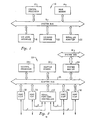
- a computer system referred to generally as a host system, is indicated by reference number 10.
- the system 10 includes a central processor 12 and a main memory 14 connected to a system bus 16.
- One or more user interface input/output devices 18 are also connected to the bus 16. These user interface devices 18 typically comprise a display and keyboard, and often include a pointing device such as a mouse.
- a mass storage input/output device 20 is also preferably connected to bus 16, and interfaces the system 10 with one or more mass storage devices. These devices typically include magnetic or optical disk drives. Some systems do not include such mass storage devices 20, instead relying upon remote mass storage devices connected to a network.
- An adapter for serial input/output devices 22 is preferably connected to system bus 16. In a preferred embodiment, such adapter 22 provides communications between the system 10 and multiple serial communications ports. Various other devices may be included in the system 10 as known in the art.
- the system of Figure 1 shows all of the input/output devices as being connected to the main system bus 16.
- Many high performance systems provide a high speed bus between the central processor 12 and main memory 14.
- an input/output controller (not shown) is connected to the high speed bus, and in turn connects to the various input/output devices 18, 20, 22 through a separate input/output bus (not shown).
- data transferred between main memory 14 and the various input/output devices is routed through, and controlled by, the input/output controller.
- the multiple-port serial adapter described below can function equally well in a system of either type. It is only necessary to provide an appropriate interface between the adapter and the bus to allow it to be used in many different types of computer systems.
- Adapter 22 is connected to the system bus 16 through a system bus interface 24.
- Interface 24 is connected to an adapter bus 26, which is a high speed bus.
- adapter bus 26 Also connected to adapter bus 26 are a central processor 28 and an adapter memory 30.
- Central processor 28 can be a commercially available microprocessor, such as an INTEL 80186 processor.
- Adapter memory 30 is a computer system memory as known in the art, and is made available in an amount sufficient to support the functions described below. In typical applications, 512K bytes of adapter memory 30 are sufficient for four communications ports.
- Central processor 28 executes the functions of the adapter 22 using programs stored in the memory 30.
- adapter bus 26 Also connected to adapter bus 26 are four serial port interfaces 32, 34, 36, and 38. Although four ports are shown in Figure 2, more can be included on a single adapter if desired. The number of ports which can be included on a single adapter card 22 is limited only by the processing power which is available to serve the ports, and the number of physical port connections which can be made to the adapter card 22.
- a serial port DMA controller 40 is connected to the adapter bus 26, and is used to control DMA transfers between the ports 32, 34, 36, 38 and the adapter memory 30.
- Each port has two signal lines connected directly to the DMA controller 40 to indicate when data is available in a receive buffer and when a transmit buffer is available to accept data.
- the DMA controller 40 uses such signals to determine when to initiate a DMA transfer between a communications port and adapter memory 30.
- the DMA controller 40 and the system bus interface 24 are both capable of acting as bus masters of the adapter bus 26 in order to perform DMA transfers.
- Bus system interface 24 and DMA controller 40 use DMA to transfer data to and from adapter memory 30.
- interface 24 can also become a bus master for system bus 16, and transfer data to and from main memory 14 using a DMA channel.
- a single DMA channel is used by system bus interface 24 to transfer data for all of the communications ports 32, 34, 36, and 38.
- central processor 28 executes a number of different routines which will be described below. Of notable importance is a task scheduler routine which determines which task is to be executed next. Various routines for setting up DMA transfer to and from the system bus 16 through the system bus interface 24, setting up transmit and receive operations between the adapter memory 30 and the communications ports, and for handling various error conditions, are executed by the central processor 28.
- Figure 3 shows a schedule work table 50 preferably used for scheduling tasks on the adapter. Different tasks operate at different priority levels, with priority levels 0-6 being shown in Figure 3. The number of priority levels actually used can be varied as needed to suit any particular implementation. Priority level 0 is the highest priority, with priority level 6 being the lowest priority.
- Each priority level has an entry which is indicative of those tasks waiting to be performed.
- Priority levels 1-6 each consist of a bitmap having one entry corresponding to each communications port on the adapter. If any particular bit has a value of one, the corresponding port has the corresponding task scheduled.
- the bits in the scheduler work table 50 are set by various interrupt handlers and by executing tasks as described in more detail below.
- the appropriate handler determines which routine should be invoked to process it, and schedules such routine by setting a bit in the scheduler work table 50.
- a routine executes, it can schedule other routines by setting bits in the table 50, and will generally unschedule itself by resetting its own bit.
- the highest priority level, level 0 is used as a counter to indicate the number of currently scheduled tasks for that priority level. This difference in operation will be described in further detail below. In some implementations, it may be desirable to use other priority levels, or none at all, in this manner.
- the highest priority level is the task which performs the system bus DMA transfers. Whenever a task needs to perform system bus DMA, it increments the level 0 counter and places necessary identifying information into a list in memory 30. Since only a single system bus DMA channel is available, only one system DMA task can operate at any given time. Any remaining tasks must wait until the currently executing system bus DMA task completes before they can be executed. Other tasks can be executed on the adapter while a system bus DMA task is executed as will be described below.
- the level 1 task is called when a frame has been received over a communications port, and various steps must be taken to check the validity of the received frame.
- the receive data task causes a received frame to be examined, and any errors flagged.
- the receive data task also schedules a system bus DMA transfer of the received frame to the host.
- the next priority task, level 2 is the transmit data task. This task initiates the transfer of data from the adapter memory 30 to the appropriate communications port.
- a transmit data task is scheduled when a frame of data for communications over a port has been assembled, or when a previous frame completes transmission.
- the level 3 task is an error/status task which is invoked whenever an error appears on a communications port.
- the types of errors handled by this task preferably include line errors, such as unexpected changes in control signals, as well as data transmission errors.
- Level 4 is a task which processes the entries in a port response queue.
- level 5 is a task which processes commands which are sent to a port which have been queued to await later processing.
- Use of the port response queue and port command queue allows various types of processing to be performed without waiting for a communications port to finish its current operation. For example, commands can be sent to a port when it is convenient for the host system, and they will reside in the queue until they can be applied to the port. Incoming events are stored in the port response queue until they are can be handled by the central processor 28 on the adapter 22.
- the lowest priority level, level 6 is used to wake up tasks which have been put to sleep. Sometimes it is desirable to suspend operation of a task until a predefined event occurs. This task can be put to sleep as will be described below, and will remain suspended.
- an interrupt handler associated with the event schedules the port response queue task, which in turn causes the appropriate bit to be set for level 6 of the scheduler work table 50.
- the wakeup task is selected to be executed for that port, the suspended task resumes execution.
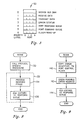
- Figures 4(a), 4(b) and 4(c) illustrate the manner in which tasks are scheduled and executed.
- the scheduler is seen to execute in an endless loop.
- a currently selected task, or process is executed to completion 60.
- the scheduler selects the highest priority level which has any task scheduled 62. Within that priority level, the scheduler then selects a task to be executed. If more than one task is scheduled to be executed at the selected priority level, a round-robin strategy is used to determine which task is to be executed next. This ensures that all ports will be equally treated, and that no port will have a task executed at any given priority level until all other ports having a task scheduled at the same priority level have been serviced.
- control returns to step 60 and the selected task is executed.
- Steps 62 and 64 operate very quickly, and preferably are made uninterruptable. This is because the various interrupts which may occur often schedule tasks by updating the scheduler work table 50, and this activity would interfere with the selection process of steps 62 and 64.
- Process execution in step 60 is interruptible, and various hardware interrupts generated by the system and communications ports are used to schedule further tasks within the scheduler work table 50.
- FIG. 4(b) shows the general method by which an interrupt is handled.
- control of the central processor 28 is vectored to a general interrupt routine.
- This routine identifies the nature of the interrupt which occurred 66, and causes the appropriate interrupt handler to be executed 68.
- the interrupt handler which executes in step 68 is preferably very short, and is made non-interruptible. It typically clears the cause of the interrupt, copies one or two data items to an appropriate area where they can be found by one of the regularly scheduled tasks, and updates the scheduler work table 70 to cause the appropriate task to be scheduled.
- additional tasks are scheduled in work table 50 by the various interrupt handlers which are executed.
- the method of Figure 4(b) is used when the various tasks are made non-preemptable. In other words, an executing task is completed before another task is initialized by the scheduler. Since most tasks are fairly short, this does not present a problem in most systems. However, if desired, the various tasks can be made preemptable. If this is done, scheduling of a higher priority task by an interrupt causes the execution of the current task to be suspended and the higher priority task to be executed immediately. A flowchart of interrupt handling in such a situation is shown in Figure 4(c).
- interrupt handler When a hardware interrupt occurs, the nature of the interrupt is identified 72 and an appropriate interrupt handler executed 74. As before, executing the interrupt handler causes the scheduler work table 50 to be updated 76. A check is then made 78 to see whether work having a higher priority than the currently executing task has been scheduled. If a higher priority task has not been scheduled 80, execution of the current task resumes. If a higher priority task was scheduled during execution of the interrupt handler 74, the currently executing process is preempted 82 and the scheduler invoked again to initiate execution of the higher priority process.
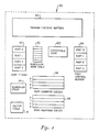
- transmit/receive buffers 90 are dynamically allocated from free space available within the memory 30. A list of free space available for the transmit/receive buffers 90 is maintained as known in the art.
- a vector table 91 is allocated for use by the various tasks and interrupts.
- Stacks 92 are allocated for temporary data storage for each port independently. Thus, four stacks are allocated within memory 30 when four communications ports are provided on the adapter.
- a separate stack 93 is used by the scheduler.
- Each port also has a port control block 94 which contains pointers to various data structures which are accessed by the corresponding port.
- Port command queue 96 provides a FIFO queue for each port which contains commands sent to the port. Each command sent to a port is placed into a standard sized data structure referred to as a port command element, and the commands for each queue are placed into a circular buffer.
- a port command When a port command is executed which requires data to be transmitted to or from the host, further commands may not be executed for such port until the data transfer process is completed.
- Each port also has a corresponding port response queue 98, which is comprised of a circular buffer in the same matter as the port command queue 96.
- the port response queues 98 contain entries generated by the corresponding ports which must be processed by the system. If a system bus DMA transfer is being performed for a port, all such responses being generated by the port must be routed to the port response queue 98. Also, if a port is sleeping, to be awakened by the occurrence of a predetermined event, all responses generated by the port are routed into the appropriate response queue 98.
- adapter memory 30 Also found within the adapter memory 30 is the executable code 100 for the scheduler, the various scheduled tasks, and the interrupt handlers. Various other locations, used for temporary variable storage as known in the art, are located in adapter memory 30, but are not specifically shown in Figure 5. Scheduler work table 50 is also contained in memory 30.
- the system bus DMA task uses the scheduler work table 50 differently from the other levels, in that the scheduler work table entry indicates the number of tasks which are scheduled rather than identifying the ports which have a task scheduled.
- the scheduler work table entry indicates the number of tasks which are scheduled rather than identifying the ports which have a task scheduled.
- an indication of the requested task is stored in a separate data structure (not shown), and one of the scheduled system bus DMA tasks is selected according to any desired prioritizing scheme.
- the first step performed by a selected system bus DMA task is to save the current DMA count 108 as reflected in level 0 of the scheduler work table 50.
- a 0 entry is then made for level 0 of the scheduler work table 110, and the system bus DMA task is initiated 112.
- DMA is initiated 112 control can be returned to the scheduler to select another task for execution.
- the system bus DMA transfer will be completed 114.
- an additional task must be scheduled 116, and the scheduler work table level 0 entry is restored 118.
- the value placed back into level 0 of the table 50 is preferably decremented before it is restored.
- a transmit DMA which moves data from the host system onto the adapter 22, it is necessary to remove any locks (described below) which have been placed on the port command queue.
- a port command queue task is scheduled.
- a receive DMA which transfers data from the adapter 22 to the host system, completes, a port response queue task is scheduled.
- a global flag which causes routing of response events for that port into the port response queue is cleared to allow port responses to be handled normally. All of these actions occur in step 116.
- Figure 7 illustrates operation of the transmit data task.
- This task is scheduled when an end of frame interrupt indicates completion of a transmit operation through a port.
- the task first signals completion 120 by placing the relevant information into the port control block 94.
- the transmit buffer is then cleared and freed 122.
- the port command queue task is scheduled 124 by setting the appropriate bit in the scheduler work table 50. If another frame is ready for transmission 126, the transmission is initiated 128 and the task completes. If no frame is ready for transmission 126, the task simply returns.
- Figure 8 shows the steps performed by the receive data task.
- a procedure which has been coded specifically to handle the communications protocol being used on the communications port is called 130.
- the protocol used on a communications port is indicated by appropriate values contained within the corresponding port control block 94.
- the steps shown in block 132 are actually performed by the protocol specific procedure.
- the received frame is processed 134 and any appropriate entries are added to the response queue 136. If errors occur within the received data frame, an error/status task can be scheduled.
- Figure 9 shows the steps performed by the error/status task.
- An error identifier is copied by the interrupt handler to the port control block 140 for the port in order to indicate to later tasks which access that port that an error has occurred.
- the error identifier indicates the type of error which has occurred and the corresponding possible error sources are checked 142. Once the source of the error has been identified, appropriate entries are added to the response queue 144 for that port. When these entries are eventually processed, the port errors will be indicated to the system 10.
- FIG. 10 Operation of the port response queue task is illustrated in Figure 10.
- a check is first made to see whether the queue is empty 150. If so, the flag which is used to automatically reroute port responses to the queue is cleared 152, causing port responses to be handled in the normal manner.
- the task then unschedules itself 154 from the scheduler work table 50 and completes. If there are entries in the queue 150, the next one is selected 156.
- a check is made 158 to see if the next entry is a response which requires a DMA transfer to be made to the host system 10. If so, the bus master DMA task is scheduled 160 and the current task is unscheduled 154. If the next entry is not a DMA transfer, a check is made to see whether a task is sleeping for the port 162. If not, the response is sent to the host 164. If a task is sleeping, the sleep/wakeup task is scheduled 166 and the current task is unscheduled 154.
- Figure 11 illustrates the steps performed by the port command queue task.
- this task selects the next entry in the port command queue 96 and causes it to be executed. The occurrence of various events may prevent execution of the next port command entry from occurring.
- the first step is to select the next entry 170 from the port command queue. If the next entry is not locked 172, a check is made to see whether a system bus DMA operation is required 174. If not, and the port is otherwise available 176, transmission of the next data block is set up 177 and the transfer data task is scheduled 178. As described above, up to two transmits can be preprocessed if two ping-pong buffers are provided for each port.
- step 174 it is necessary to perform a system bus DMA transfer to transfer data onto the adapter 22 before the data can be transmitted. If the test of step 174 results in a YES response, it is necessary to schedule an appropriate system DMA activity 180 and lock the currently selected entry of the port command queue 182. The level 5 task for this port is then unscheduled 184. As described above in connection with Figure 6, completion of the system bus DMA task causes the lock set in step 182 to be removed, and the port command queue task for this port to be rescheduled. The next time through the process of Figure 11, the system DMA test of step 174 will result in a NO response. If the next entry is locked in step 172, or the port is not available in step 176, control transfers to step 184 and the level 5 entry for this port in the scheduler work table 50 is unscheduled 184.
- Figure 12 illustrates the steps which are performed when a task puts itself to sleep and is subsequently awakened.
- a SLEEP ENABLE variable is first set for the port 190.
- the task goes to sleep 191 and the current context is saved to the stack 192 for the port.
- Setting the SLEEP ENABLE variable in step 190 causes any responses generated by the port to be routed to the port response queue 98.
- the task which is going to sleep is then exited and other processing occurs 194. While other processing occurs, the context which was saved in step 192 remains untouched on the port stack 92.
- the port response queue task wakes up the sleeping task and the context is restored from the stack 196.
- the SLEEP ENABLE variable is reset. The task can put itself back to sleep at a later stage in its execution, which causes the described sequence of events to repeat.
- waking a sleeping task is the lowest level task which can be scheduled, the system is guaranteed to have the context which was saved to the stack in step 192 as the top frame on the stack when the wakeup is received.
- a wakeup is scheduled by another task or interrupt, which sets the appropriate bit on level 6 on the scheduler work table 50.
- the system described above provides for priority scheduling of various communications subtasks on the adapter.
- the number of priority levels and the number of communications ports which can be supported are easily expanded without changing the underlying scheduler.
- the adapter of the preferred embodiment supports two separate levels of DMA transfer. One level is the DMA transfer performed over the adapter bus 26, and the second level is the DMA transfer over the system bus 16 performed by the system bus interface 24.
- Tasks have been prioritized by the preferred scheduler work table 50 so that the most time critical tasks have the highest priority.
- the transmit data and the receive data tasks which must be performed in a timely manner to avoid data loss through the communications port, have a higher priority than handling of the various commands and responses placed in the queues 96 and 98.
- System bus DMA transfer tends to be the bottleneck because one resource is shared among all ports, so the system bus DMA task is given the highest priority.
- a mechanism is provided whereby other tasks are performed on the adapter 22 while a system bus DMA transfer is taking place. Since a round robin strategy is used for each priority level, no port becomes starved.
Abstract
Description
- The present invention relates generally to digital computer systems, and more specifically to adapters for interfacing host computer systems with serial communication lines.
- Communications with the outside world are extremely important to modern computer systems. Some systems have several serial communications links which operate simultaneously. Controlling multiple links operating simultaneously can place demands on a system processor which degrade overall system performance.
- One solution to this performance problem is to use "smart" communications adapters. These adapters handle all of the low level details of a communications session. The adapters communicate with their host system to transfer data in relatively large blocks. Both received data and data to the transmitted are transferred between the adapter and the host system using block transfers. Direct memory access (DMA) can be used for such transfers to further reduce the processing burden placed on the host central processor.
- On order to provide multiple communications ports in a system having a limited number of adapters, several ports can be placed on a single adapter. However, this approach can lead to significant problems. Data and command handling for several independent ports can become quite complex, especially at high communications rates. When different speeds and protocols are used on the different communications ports, the problem becomes greatly exacerbated. It becomes difficult for the adapter to ensure that all communications ports are handled in a timely manner.
- Accordingly the invention provides a communications adapter for interfacing a plurality of communications ports with a host system, comprising: an interface to the host system; an intermediate memory; a processor for controlling operation of the adapter; a plurality of communications ports; a bus connecting said host interface, said intermediate memory, said processor and said communications ports; and means for scheduling execution of a plurality of communications tasks to be executed by said processor.
- A single adapter can support multiple communications ports where each port operates independently of the others. The communications ports are handled in such a manner as to ensure that no data is lost on any port. In such a system, a scheduler executing on the adapter can schedule tasks at different priority levels, so that time-critical tasks are performed quickly enough to prevent data loss. Data to be transmitted or received through a communications port can be stored in buffers on the adapter, and data and command communications between the adapter and the host system are preferably performed over a DMA channel.
- The invention also provides a method for controlling data transfer between a host system and a plurality of communications ports, comprising the steps of: defining a plurality of tasks for performing data transfer (or portions thereof) between the ports and an intermediate memory, and between the intermediate memory and the host system; assigning priorities to the defined tasks; scheduling tasks to be performed in response to events which occur at the ports and within the host system; and when a task is completed, selecting to be performed next a task having the highest priority of all scheduled tasks.
- Preferably there is a table having an entry for each task, and the tasks are scheduled by writing information to the corresponding table entry. At least one entry in the table has a plurality of subentries each corresponding to a respective port, and the task is scheduled to be performed for a port by writing information to the corresponding subentry. Preferably, at least one entry in the table represents a count of the number of times the corresponding task has been scheduled, and a task is scheduled by incrementing the value in the entry.
- It is also preferred that the events which cause tasks to be scheduled comprises hardware interrupts raised by the host system or by the ports, or also by the execution of scheduled tasks. Each task is assigned a priority level, and the scheduled tasks having a higher priority level are performed before the scheduled tasks having a lower priority level.
-
- Figure 1 is a block diagram of a host computer system;
- Figure 2 is a block diagram of a preferred serial communications adapter for use with the system of Figure 1;
- Figure 3 illustrates a preferred scheduler work table;
- Figure 4 is a set of flow charts illustrating execution of tasks and interrupts on an adapter system;
- Figure 5 illustrates contents of a memory included on an adapter; and
- Figures 6 through 12 are flow charts illustrating operation of selected functions which can be scheduled in accordance with the method of the present invention.
- Referring to Figure 1, a computer system, referred to generally as a host system, is indicated by
reference number 10. Thesystem 10 includes a central processor 12 and a main memory 14 connected to a system bus 16. One or more user interface input/output devices 18 are also connected to the bus 16. These user interface devices 18 typically comprise a display and keyboard, and often include a pointing device such as a mouse. - A mass storage input/
output device 20 is also preferably connected to bus 16, and interfaces thesystem 10 with one or more mass storage devices. These devices typically include magnetic or optical disk drives. Some systems do not include suchmass storage devices 20, instead relying upon remote mass storage devices connected to a network. An adapter for serial input/output devices 22 is preferably connected to system bus 16. In a preferred embodiment,such adapter 22 provides communications between thesystem 10 and multiple serial communications ports. Various other devices may be included in thesystem 10 as known in the art. - The system of Figure 1 shows all of the input/output devices as being connected to the main system bus 16. Many high performance systems provide a high speed bus between the central processor 12 and main memory 14. In such systems, an input/output controller (not shown) is connected to the high speed bus, and in turn connects to the various input/
output devices - Referring to Figure 2, a preferred serial input/
output adapter 22 is shown.Adapter 22 is connected to the system bus 16 through a system bus interface 24. Interface 24 is connected to anadapter bus 26, which is a high speed bus. Also connected toadapter bus 26 are a central processor 28 and an adapter memory 30. Central processor 28 can be a commercially available microprocessor, such as an INTEL 80186 processor. Adapter memory 30 is a computer system memory as known in the art, and is made available in an amount sufficient to support the functions described below. In typical applications, 512K bytes of adapter memory 30 are sufficient for four communications ports. Central processor 28 executes the functions of theadapter 22 using programs stored in the memory 30. - Also connected to
adapter bus 26 are fourserial port interfaces single adapter card 22 is limited only by the processing power which is available to serve the ports, and the number of physical port connections which can be made to theadapter card 22. - A serial
port DMA controller 40 is connected to theadapter bus 26, and is used to control DMA transfers between theports DMA controller 40 to indicate when data is available in a receive buffer and when a transmit buffer is available to accept data. TheDMA controller 40 uses such signals to determine when to initiate a DMA transfer between a communications port and adapter memory 30. - The
DMA controller 40 and the system bus interface 24 are both capable of acting as bus masters of theadapter bus 26 in order to perform DMA transfers. Bus system interface 24 andDMA controller 40 use DMA to transfer data to and from adapter memory 30. In addition, interface 24 can also become a bus master for system bus 16, and transfer data to and from main memory 14 using a DMA channel. In the embodiment described herein, a single DMA channel is used by system bus interface 24 to transfer data for all of thecommunications ports - In order to control operation of the
adapter 22, central processor 28 executes a number of different routines which will be described below. Of notable importance is a task scheduler routine which determines which task is to be executed next. Various routines for setting up DMA transfer to and from the system bus 16 through the system bus interface 24, setting up transmit and receive operations between the adapter memory 30 and the communications ports, and for handling various error conditions, are executed by the central processor 28. - Figure 3 shows a schedule work table 50 preferably used for scheduling tasks on the adapter. Different tasks operate at different priority levels, with priority levels 0-6 being shown in Figure 3. The number of priority levels actually used can be varied as needed to suit any particular implementation.
Priority level 0 is the highest priority, withpriority level 6 being the lowest priority. - Each priority level has an entry which is indicative of those tasks waiting to be performed. Priority levels 1-6 each consist of a bitmap having one entry corresponding to each communications port on the adapter. If any particular bit has a value of one, the corresponding port has the corresponding task scheduled.
- The bits in the scheduler work table 50 are set by various interrupt handlers and by executing tasks as described in more detail below. When a hardware interrupt occurs, the appropriate handler determines which routine should be invoked to process it, and schedules such routine by setting a bit in the scheduler work table 50. When a routine executes, it can schedule other routines by setting bits in the table 50, and will generally unschedule itself by resetting its own bit.
- The highest priority level,
level 0, is used as a counter to indicate the number of currently scheduled tasks for that priority level. This difference in operation will be described in further detail below. In some implementations, it may be desirable to use other priority levels, or none at all, in this manner. - The highest priority level is the task which performs the system bus DMA transfers. Whenever a task needs to perform system bus DMA, it increments the
level 0 counter and places necessary identifying information into a list in memory 30. Since only a single system bus DMA channel is available, only one system DMA task can operate at any given time. Any remaining tasks must wait until the currently executing system bus DMA task completes before they can be executed. Other tasks can be executed on the adapter while a system bus DMA task is executed as will be described below. - The
level 1 task is called when a frame has been received over a communications port, and various steps must be taken to check the validity of the received frame. The receive data task causes a received frame to be examined, and any errors flagged. The receive data task also schedules a system bus DMA transfer of the received frame to the host. - The next priority task,
level 2, is the transmit data task. This task initiates the transfer of data from the adapter memory 30 to the appropriate communications port. A transmit data task is scheduled when a frame of data for communications over a port has been assembled, or when a previous frame completes transmission. - The
level 3 task is an error/status task which is invoked whenever an error appears on a communications port. The types of errors handled by this task preferably include line errors, such as unexpected changes in control signals, as well as data transmission errors. - Under circumstances which will be described below, various events which are generated by a port which is transmitting or receiving data must be queued to await later processing.
Level 4 is a task which processes the entries in a port response queue. In a similar manner,level 5 is a task which processes commands which are sent to a port which have been queued to await later processing. Use of the port response queue and port command queue allows various types of processing to be performed without waiting for a communications port to finish its current operation. For example, commands can be sent to a port when it is convenient for the host system, and they will reside in the queue until they can be applied to the port. Incoming events are stored in the port response queue until they are can be handled by the central processor 28 on theadapter 22. - The lowest priority level,
level 6, is used to wake up tasks which have been put to sleep. Sometimes it is desirable to suspend operation of a task until a predefined event occurs. This task can be put to sleep as will be described below, and will remain suspended. When the predetermined event occurs, an interrupt handler associated with the event schedules the port response queue task, which in turn causes the appropriate bit to be set forlevel 6 of the scheduler work table 50. When the wakeup task is selected to be executed for that port, the suspended task resumes execution. - Figures 4(a), 4(b) and 4(c) illustrate the manner in which tasks are scheduled and executed. Referring to figure 4(a), the scheduler is seen to execute in an endless loop. A currently selected task, or process, is executed to
completion 60. When execution of the task is complete, the scheduler selects the highest priority level which has any task scheduled 62. Within that priority level, the scheduler then selects a task to be executed. If more than one task is scheduled to be executed at the selected priority level, a round-robin strategy is used to determine which task is to be executed next. This ensures that all ports will be equally treated, and that no port will have a task executed at any given priority level until all other ports having a task scheduled at the same priority level have been serviced. After the task has been selected, control returns to step 60 and the selected task is executed. -
Steps steps step 60 is interruptible, and various hardware interrupts generated by the system and communications ports are used to schedule further tasks within the scheduler work table 50. - Figure 4(b) shows the general method by which an interrupt is handled. When a hardware interrupt occurs on the
adapter 22, control of the central processor 28 is vectored to a general interrupt routine. This routine identifies the nature of the interrupt which occurred 66, and causes the appropriate interrupt handler to be executed 68. The interrupt handler which executes instep 68 is preferably very short, and is made non-interruptible. It typically clears the cause of the interrupt, copies one or two data items to an appropriate area where they can be found by one of the regularly scheduled tasks, and updates the scheduler work table 70 to cause the appropriate task to be scheduled. Thus, while a task is executing instep 60, additional tasks are scheduled in work table 50 by the various interrupt handlers which are executed. - The method of Figure 4(b) is used when the various tasks are made non-preemptable. In other words, an executing task is completed before another task is initialized by the scheduler. Since most tasks are fairly short, this does not present a problem in most systems. However, if desired, the various tasks can be made preemptable. If this is done, scheduling of a higher priority task by an interrupt causes the execution of the current task to be suspended and the higher priority task to be executed immediately. A flowchart of interrupt handling in such a situation is shown in Figure 4(c).
- When a hardware interrupt occurs, the nature of the interrupt is identified 72 and an appropriate interrupt handler executed 74. As before, executing the interrupt handler causes the scheduler work table 50 to be updated 76. A check is then made 78 to see whether work having a higher priority than the currently executing task has been scheduled. If a higher priority task has not been scheduled 80, execution of the current task resumes. If a higher priority task was scheduled during execution of the interrupt handler 74, the currently executing process is preempted 82 and the scheduler invoked again to initiate execution of the higher priority process.
- Referring to Figure 5, some of the important data structures stored within the adapter memory 30 are shown. The major portion of memory 30 is preferably taken up by transmit/receive buffers 90. These buffers 90 are dynamically allocated from free space available within the memory 30. A list of free space available for the transmit/receive buffers 90 is maintained as known in the art.
- A vector table 91 is allocated for use by the various tasks and interrupts. Stacks 92 are allocated for temporary data storage for each port independently. Thus, four stacks are allocated within memory 30 when four communications ports are provided on the adapter. A separate stack 93 is used by the scheduler. Each port also has a
port control block 94 which contains pointers to various data structures which are accessed by the corresponding port.Port command queue 96 provides a FIFO queue for each port which contains commands sent to the port. Each command sent to a port is placed into a standard sized data structure referred to as a port command element, and the commands for each queue are placed into a circular buffer. - When a port command is executed which requires data to be transmitted to or from the host, further commands may not be executed for such port until the data transfer process is completed. In some systems, it is possible to use ping-pong buffers to transfer data through a port. In such cases, if one channel of a port is active, the other channel may be set up for the next transfer. Port commands waiting in the
port command queue 96 may be executed in order to prepare the other buffer. - Each port also has a corresponding
port response queue 98, which is comprised of a circular buffer in the same matter as theport command queue 96. Theport response queues 98 contain entries generated by the corresponding ports which must be processed by the system. If a system bus DMA transfer is being performed for a port, all such responses being generated by the port must be routed to theport response queue 98. Also, if a port is sleeping, to be awakened by the occurrence of a predetermined event, all responses generated by the port are routed into theappropriate response queue 98. - Also found within the adapter memory 30 is the
executable code 100 for the scheduler, the various scheduled tasks, and the interrupt handlers. Various other locations, used for temporary variable storage as known in the art, are located in adapter memory 30, but are not specifically shown in Figure 5. Scheduler work table 50 is also contained in memory 30. - Referring to Figure 6, operation of the system bus DMA task is shown. As described above, the system bus DMA task uses the scheduler work table 50 differently from the other levels, in that the scheduler work table entry indicates the number of tasks which are scheduled rather than identifying the ports which have a task scheduled. When a system bus DMA task is scheduled, an indication of the requested task is stored in a separate data structure (not shown), and one of the scheduled system bus DMA tasks is selected according to any desired prioritizing scheme.
- Once a system bus DMA task has been is initiated, other adapter processing may be performed while the transfer is taking place. Since the scheduler will attempt to schedule a
level 0 task if possible, it is necessary to set thelevel 0 entry to 0 for the duration of the system bus DMA transfer. Thus, referring to Figure 6, the first step performed by a selected system bus DMA task is to save the current DMA count 108 as reflected inlevel 0 of the scheduler work table 50. A 0 entry is then made forlevel 0 of the scheduler work table 110, and the system bus DMA task is initiated 112. Once DMA is initiated 112, control can be returned to the scheduler to select another task for execution. - At some future time, the system bus DMA transfer will be completed 114. At this time, an additional task must be scheduled 116, and the scheduler
work table level 0 entry is restored 118. The value placed back intolevel 0 of the table 50 is preferably decremented before it is restored. - If a transmit DMA has occurred, which moves data from the host system onto the
adapter 22, it is necessary to remove any locks (described below) which have been placed on the port command queue. In addition, a port command queue task is scheduled. When a receive DMA, which transfers data from theadapter 22 to the host system, completes, a port response queue task is scheduled. In addition, a global flag which causes routing of response events for that port into the port response queue is cleared to allow port responses to be handled normally. All of these actions occur in step 116. - Figure 7 illustrates operation of the transmit data task. This task is scheduled when an end of frame interrupt indicates completion of a transmit operation through a port. The task first signals completion 120 by placing the relevant information into the
port control block 94. The transmit buffer is then cleared and freed 122. The port command queue task is scheduled 124 by setting the appropriate bit in the scheduler work table 50. If another frame is ready fortransmission 126, the transmission is initiated 128 and the task completes. If no frame is ready fortransmission 126, the task simply returns. - Figure 8 shows the steps performed by the receive data task. First, a procedure which has been coded specifically to handle the communications protocol being used on the communications port is called 130. The protocol used on a communications port is indicated by appropriate values contained within the corresponding
port control block 94. The steps shown inblock 132 are actually performed by the protocol specific procedure. The received frame is processed 134 and any appropriate entries are added to theresponse queue 136. If errors occur within the received data frame, an error/status task can be scheduled. - Figure 9 shows the steps performed by the error/status task. An error identifier is copied by the interrupt handler to the port control block 140 for the port in order to indicate to later tasks which access that port that an error has occurred. The error identifier indicates the type of error which has occurred and the corresponding possible error sources are checked 142. Once the source of the error has been identified, appropriate entries are added to the
response queue 144 for that port. When these entries are eventually processed, the port errors will be indicated to thesystem 10. - Operation of the port response queue task is illustrated in Figure 10. A check is first made to see whether the queue is empty 150. If so, the flag which is used to automatically reroute port responses to the queue is cleared 152, causing port responses to be handled in the normal manner. The task then unschedules itself 154 from the scheduler work table 50 and completes. If there are entries in the
queue 150, the next one is selected 156. A check is made 158 to see if the next entry is a response which requires a DMA transfer to be made to thehost system 10. If so, the bus master DMA task is scheduled 160 and the current task is unscheduled 154. If the next entry is not a DMA transfer, a check is made to see whether a task is sleeping for theport 162. If not, the response is sent to thehost 164. If a task is sleeping, the sleep/wakeup task is scheduled 166 and the current task is unscheduled 154. - Figure 11 illustrates the steps performed by the port command queue task. In general, this task selects the next entry in the
port command queue 96 and causes it to be executed. The occurrence of various events may prevent execution of the next port command entry from occurring. The first step is to select thenext entry 170 from the port command queue. If the next entry is not locked 172, a check is made to see whether a system bus DMA operation is required 174. If not, and the port is otherwise available 176, transmission of the next data block is set up 177 and the transfer data task is scheduled 178. As described above, up to two transmits can be preprocessed if two ping-pong buffers are provided for each port. - In many cases, it is necessary to perform a system bus DMA transfer to transfer data onto the
adapter 22 before the data can be transmitted. If the test ofstep 174 results in a YES response, it is necessary to schedule an appropriatesystem DMA activity 180 and lock the currently selected entry of theport command queue 182. Thelevel 5 task for this port is then unscheduled 184. As described above in connection with Figure 6, completion of the system bus DMA task causes the lock set instep 182 to be removed, and the port command queue task for this port to be rescheduled. The next time through the process of Figure 11, the system DMA test ofstep 174 will result in a NO response. If the next entry is locked instep 172, or the port is not available instep 176, control transfers to step 184 and thelevel 5 entry for this port in the scheduler work table 50 is unscheduled 184. - Figure 12 illustrates the steps which are performed when a task puts itself to sleep and is subsequently awakened. A SLEEP ENABLE variable is first set for the
port 190. The task goes tosleep 191 and the current context is saved to the stack 192 for the port. Setting the SLEEP ENABLE variable instep 190 causes any responses generated by the port to be routed to theport response queue 98. The task which is going to sleep is then exited and other processing occurs 194. While other processing occurs, the context which was saved in step 192 remains untouched on the port stack 92. - When new events are added to the port response queue, the port response queue task wakes up the sleeping task and the context is restored from the stack 196. A check is made 198 to determine whether the wakeup event was a terminal condition for which the task is waiting 198. If not, the task simply goes back to
sleep 191. If the event actually causes the task to wake up, execution is resumed 200. When the task completes, the SLEEP ENABLE variable is reset. The task can put itself back to sleep at a later stage in its execution, which causes the described sequence of events to repeat. - Since waking a sleeping task is the lowest level task which can be scheduled, the system is guaranteed to have the context which was saved to the stack in step 192 as the top frame on the stack when the wakeup is received. A wakeup is scheduled by another task or interrupt, which sets the appropriate bit on
level 6 on the scheduler work table 50. - The system described above provides for priority scheduling of various communications subtasks on the adapter. The number of priority levels and the number of communications ports which can be supported are easily expanded without changing the underlying scheduler. The adapter of the preferred embodiment supports two separate levels of DMA transfer. One level is the DMA transfer performed over the
adapter bus 26, and the second level is the DMA transfer over the system bus 16 performed by the system bus interface 24. - Tasks have been prioritized by the preferred scheduler work table 50 so that the most time critical tasks have the highest priority. The transmit data and the receive data tasks, which must be performed in a timely manner to avoid data loss through the communications port, have a higher priority than handling of the various commands and responses placed in the
queues adapter 22 while a system bus DMA transfer is taking place. Since a round robin strategy is used for each priority level, no port becomes starved.
Claims (15)
- A method for controlling data transfer between a host system (10) and a plurality of communications ports (32,34), comprising the steps of:
defining a plurality of tasks for performing data transfer between the ports and an intermediate memory (30), and between the intermediate memory and the host system;
assigning priorities to the defined tasks;
scheduling tasks (70) to be performed in response to events which occur at the ports and within the host system; and
when a task is completed, selecting (62) to be performed next a task having the highest priority of all scheduled tasks. - The method of Claim 1, wherein a task is performed for all ports for which it is scheduled using a round robin strategy.
- The method of Claim 1 or 2, wherein said scheduling step includes the step of:
providing a table (50) having an entry for each defined task, wherein tasks are scheduled by writing information to the corresponding table entry. - The method of Claim 3, wherein at least one entry in the table has a plurality of subentries each corresponding to a respective port, and wherein the task is scheduled to be performed for a port by writing information to the corresponding subentry.
- The method of Claim 4, wherein each subentry comprises one data bit.
- The method of Claim 3, 4 or 5, wherein at least one entry in the table represents a count of the number of times the corresponding task has been scheduled, and wherein a task is scheduled by incrementing the value in the entry.
- The method of any preceding Claim, wherein the events which cause tasks to be scheduled comprise hardware interrupts raised by the host system or by the ports.
- The method of Claim 7, wherein the events which cause tasks to be scheduled further comprise the execution of scheduled tasks.
- A communications adapter (22) for interfacing a plurality of communications ports (32,34) with a host system (10), comprising:
an interface to the host system (24);
an intermediate memory (30);
a processor (28) for controlling operation of the adapter;
a plurality of communications ports (32,34);
a bus (26) connecting said host interface, said intermediate memory, said processor and said communications ports; and
means (28,30) for scheduling execution of a plurality of communications tasks to be executed by said processor. - The adapter of Claim 9, further comprising means for assigning each communications task a priority level, and wherein scheduled tasks having a higher priority level are performed before scheduled tasks having a lower priority level.
- The adapter of Claim 9 or 10, wherein said scheduling means includes a table (50) having entries corresponding to said tasks, and wherein tasks are scheduled by writing information to the corresponding table entries.
- The adapter of Claim 11, further comprising means for writing information to the table entries in response to interrupts generated by the host system and said communications ports.
- The adapter of Claim 11 or 12, wherein executing tasks write information to the table entries.
- The adapter of Claim 11, 12 or 13, wherein at least one table entry contains a plurality of bits each corresponding to a respective communications port, and wherein a task is scheduled to be performed for one of said ports by writing to its corresponding bit.
- A computer system having a host system (10) including a central processor (12) and main memory (14); and an adapter (22) as claimed in any of claims 9 to 14 interfaced therwith.
Applications Claiming Priority (2)
| Application Number | Priority Date | Filing Date | Title |
|---|---|---|---|
| US07/479,777 US5247671A (en) | 1990-02-14 | 1990-02-14 | Scalable schedules for serial communications controller in data processing systems |
| US479777 | 1995-06-07 |
Publications (3)
| Publication Number | Publication Date |
|---|---|
| EP0442615A2 true EP0442615A2 (en) | 1991-08-21 |
| EP0442615A3 EP0442615A3 (en) | 1992-12-16 |
| EP0442615B1 EP0442615B1 (en) | 1998-12-16 |
Family
ID=23905385
Family Applications (1)
| Application Number | Title | Priority Date | Filing Date |
|---|---|---|---|
| EP91300418A Expired - Lifetime EP0442615B1 (en) | 1990-02-14 | 1991-01-18 | A communications adapter and method for operating it |
Country Status (10)
| Country | Link |
|---|---|
| US (1) | US5247671A (en) |
| EP (1) | EP0442615B1 (en) |
| JP (1) | JPH0727503B2 (en) |
| KR (1) | KR950002713B1 (en) |
| CN (1) | CN1021536C (en) |
| AU (1) | AU649642B2 (en) |
| DE (1) | DE69130620T2 (en) |
| MY (1) | MY105323A (en) |
| NZ (1) | NZ236764A (en) |
| SG (1) | SG42809A1 (en) |
Cited By (8)
| Publication number | Priority date | Publication date | Assignee | Title |
|---|---|---|---|---|
| WO1992017796A1 (en) * | 1991-03-28 | 1992-10-15 | The Commonwealth Of Australia | Radar control task scheduling |
| EP0523878A1 (en) * | 1991-06-28 | 1993-01-20 | Digital Equipment Corporation | Deterministic method for allocation of a shared resource |
| WO1994007196A1 (en) * | 1992-09-22 | 1994-03-31 | Unisys Corporation | Device interface module for disk drive complex |
| WO1999063448A1 (en) * | 1998-06-01 | 1999-12-09 | Advanced Micro Devices, Inc. | Universal serial bus controller with a direct memory access mode |
| EP1357477A2 (en) * | 2002-04-25 | 2003-10-29 | Infineon Technologies AG | Device connected to a bus system |
| GB2433333A (en) * | 2005-12-13 | 2007-06-20 | Advanced Risc Mach Ltd | Distributed direct memory access provision within a data processing system |
| WO2007075328A1 (en) | 2005-12-28 | 2007-07-05 | Intel Corporation | Integrated circuit capable of independently operating a plurality of communication channels |
| EP1846838A1 (en) * | 2004-12-22 | 2007-10-24 | Pika Technologies Inc. | System and method for synchronous processing of media data on an asynchronous processor |
Families Citing this family (74)
| Publication number | Priority date | Publication date | Assignee | Title |
|---|---|---|---|---|
| JP3055917B2 (en) * | 1990-05-22 | 2000-06-26 | 日本電気株式会社 | Data transfer control device |
| US5469571A (en) * | 1991-07-15 | 1995-11-21 | Lynx Real-Time Systems, Inc. | Operating system architecture using multiple priority light weight kernel task based interrupt handling |
| US5313627A (en) * | 1992-01-02 | 1994-05-17 | International Business Machines Corp. | Parity error detection and recovery |
| US5471618A (en) * | 1992-11-30 | 1995-11-28 | 3Com Corporation | System for classifying input/output events for processes servicing the events |
| US5631897A (en) * | 1993-10-01 | 1997-05-20 | Nec America, Inc. | Apparatus and method for incorporating a large number of destinations over circuit-switched wide area network connections |
| US5717870A (en) * | 1994-10-26 | 1998-02-10 | Hayes Microcomputer Products, Inc. | Serial port controller for preventing repetitive interrupt signals |
| US5634099A (en) * | 1994-12-09 | 1997-05-27 | International Business Machines Corporation | Direct memory access unit for transferring data between processor memories in multiprocessing systems |
| US5603051A (en) * | 1995-06-06 | 1997-02-11 | Hewlett-Packard Company | Input/output processor with a local memory providing shared resources for a plurality of input/output interfaces on an I/O bus |
| US6643765B1 (en) | 1995-08-16 | 2003-11-04 | Microunity Systems Engineering, Inc. | Programmable processor with group floating point operations |
| DE19535546B4 (en) * | 1995-09-25 | 2004-04-08 | Siemens Ag | Method for operating a real-time computer system controlled by a real-time operating system |
| US5925105A (en) * | 1995-12-28 | 1999-07-20 | Intel Corporation | Preventing processor domination during background data transfer in multipoint conferencing |
| US5802282A (en) * | 1995-12-28 | 1998-09-01 | Intel Corporation | Recovering missing data during background data transfer in multipoint conferencing |
| US5754776A (en) * | 1995-12-28 | 1998-05-19 | Intel Corporation | Re-prioritizing background data transfers in multipoint conferencing |
| US6400819B1 (en) * | 1996-03-28 | 2002-06-04 | Hitachi, Ltd. | Method and apparatus for executing communication in real-time and data structure for real-time data communication |
| US7116635B2 (en) * | 1996-03-28 | 2006-10-03 | Hitachi, Ltd. | Process execution method and apparatus |
| US5974496A (en) * | 1997-01-02 | 1999-10-26 | Ncr Corporation | System for transferring diverse data objects between a mass storage device and a network via an internal bus on a network card |
| US6088728A (en) * | 1997-06-11 | 2000-07-11 | Oracle Corporation | System using session data stored in session data storage for associating and disassociating user identifiers for switching client sessions in a server |
| US6243751B1 (en) | 1997-06-11 | 2001-06-05 | Oracle Corporation | Method and apparatus for coupling clients to servers |
| US6473780B1 (en) * | 1998-04-01 | 2002-10-29 | Intel Corporation | Scheduling of direct memory access |
| US6061709A (en) * | 1998-07-31 | 2000-05-09 | Integrated Systems Design Center, Inc. | Integrated hardware and software task control executive |
| US6098142A (en) * | 1998-08-25 | 2000-08-01 | Leggett; John D. | Apparatus and method for using a communications port in polling mode and without interrupts |
| US9239763B2 (en) | 2012-09-28 | 2016-01-19 | Oracle International Corporation | Container database |
| KR100617228B1 (en) * | 1999-03-19 | 2006-08-31 | 엘지전자 주식회사 | method for implementation of transferring event in real-time operating system kernel |
| JP3356110B2 (en) | 1999-04-21 | 2002-12-09 | 日本電気株式会社 | Function expansion system and data transfer method used therefor |
| US6603771B1 (en) | 1999-07-02 | 2003-08-05 | Cypress Semiconductor Corp. | Highly scalable architecture for implementing switch fabrics with quality of services |
| US6584517B1 (en) | 1999-07-02 | 2003-06-24 | Cypress Semiconductor Corp. | Circuit and method for supporting multicast/broadcast operations in multi-queue storage devices |
| US6628656B1 (en) | 1999-08-09 | 2003-09-30 | Cypress Semiconductor Corp. | Circuit, method and/or architecture for improving the performance of a serial communication link |
| US6625177B1 (en) | 1999-08-09 | 2003-09-23 | Cypress Semiconductor Corp. | Circuit, method and/or architecture for improving the performance of a serial communication link |
| WO2001016702A1 (en) | 1999-09-01 | 2001-03-08 | Intel Corporation | Register set used in multithreaded parallel processor architecture |
| ATE396449T1 (en) | 1999-09-01 | 2008-06-15 | Intel Corp | REGISTER SET FOR USE IN A PARALLEL MULTI-WIRE PROCESSOR ARCHITECTURE |
| US6477610B1 (en) * | 2000-02-04 | 2002-11-05 | International Business Machines Corporation | Reordering responses on a data bus based on size of response |
| US7089344B1 (en) * | 2000-06-09 | 2006-08-08 | Motorola, Inc. | Integrated processor platform supporting wireless handheld multi-media devices |
| US7236976B2 (en) * | 2000-06-19 | 2007-06-26 | Aramark Corporation | System and method for scheduling events and associated products and services |
| US7681018B2 (en) | 2000-08-31 | 2010-03-16 | Intel Corporation | Method and apparatus for providing large register address space while maximizing cycletime performance for a multi-threaded register file set |
| US6741530B2 (en) * | 2001-01-25 | 2004-05-25 | Dphi Acquisitions, Inc. | Time critical and non-time critical tasks control system for an optical disk using first and second processors |
| US7522480B2 (en) | 2001-01-25 | 2009-04-21 | Dphi Acquisitions, Inc. | Digital tracking servo system with multi-track seek with an acceleration clamp |
| US6868476B2 (en) | 2001-08-27 | 2005-03-15 | Intel Corporation | Software controlled content addressable memory in a general purpose execution datapath |
| US7225281B2 (en) * | 2001-08-27 | 2007-05-29 | Intel Corporation | Multiprocessor infrastructure for providing flexible bandwidth allocation via multiple instantiations of separate data buses, control buses and support mechanisms |
| US7216204B2 (en) | 2001-08-27 | 2007-05-08 | Intel Corporation | Mechanism for providing early coherency detection to enable high performance memory updates in a latency sensitive multithreaded environment |
| US7487505B2 (en) * | 2001-08-27 | 2009-02-03 | Intel Corporation | Multithreaded microprocessor with register allocation based on number of active threads |
| US20030065809A1 (en) * | 2001-10-03 | 2003-04-03 | Adc Telecommunications, Inc. | Scheduling downstream transmissions |
| US7610451B2 (en) | 2002-01-25 | 2009-10-27 | Intel Corporation | Data transfer mechanism using unidirectional pull bus and push bus |
| US7243367B2 (en) * | 2002-01-31 | 2007-07-10 | Brocade Communications Systems, Inc. | Method and apparatus for starting up a network or fabric |
| US7437724B2 (en) | 2002-04-03 | 2008-10-14 | Intel Corporation | Registers for data transfers |
| US6792481B2 (en) * | 2002-05-30 | 2004-09-14 | Freescale Semiconductor, Inc. | DMA controller |
| US7337275B2 (en) * | 2002-08-13 | 2008-02-26 | Intel Corporation | Free list and ring data structure management |
| US6941438B2 (en) | 2003-01-10 | 2005-09-06 | Intel Corporation | Memory interleaving |
| CA2514662A1 (en) * | 2003-02-11 | 2004-08-26 | Thomson Licensing | Asynchronous communications technique |
| US20040184462A1 (en) * | 2003-03-17 | 2004-09-23 | Network Equipment Technologies | Sliding window implementation for regulating packets for protocol-based connections |
| US20050021842A1 (en) * | 2003-03-17 | 2005-01-27 | Network Equipment Technologies | Real-time packet classification and rate-limiting control packets in a network processor based data-plane |
| US7353285B2 (en) * | 2003-11-20 | 2008-04-01 | International Business Machines Corporation | Apparatus, system, and method for maintaining task prioritization and load balancing |
| TWI283394B (en) * | 2004-03-31 | 2007-07-01 | Mstar Semiconductor Inc | Data processing method and structure of a multi-function display |
| US7415470B2 (en) * | 2004-08-12 | 2008-08-19 | Oracle International Corporation | Capturing and re-creating the state of a queue when migrating a session |
| US7502824B2 (en) * | 2004-08-12 | 2009-03-10 | Oracle International Corporation | Database shutdown with session migration |
| US7730257B2 (en) * | 2004-12-16 | 2010-06-01 | Broadcom Corporation | Method and computer program product to increase I/O write performance in a redundant array |
| DE102004062116B3 (en) * | 2004-12-23 | 2006-05-11 | Ab Skf | Bearing arrangement for computer tomography has bearing with inner ring, which stores construction unit, and outer ring, which is connected with damping element, fitted as single element and contain hollow cylindrical basic outline |
| US7386642B2 (en) * | 2005-01-28 | 2008-06-10 | Sony Computer Entertainment Inc. | IO direct memory access system and method |
| US7680972B2 (en) * | 2005-02-04 | 2010-03-16 | Sony Computer Entertainment Inc. | Micro interrupt handler |
| JP2006216042A (en) * | 2005-02-04 | 2006-08-17 | Sony Computer Entertainment Inc | System and method for interruption processing |
| US9176772B2 (en) * | 2005-02-11 | 2015-11-03 | Oracle International Corporation | Suspending and resuming of sessions |
| US7861113B2 (en) * | 2007-03-16 | 2010-12-28 | Dot Hill Systems Corporation | Method and apparatus for operating storage controller system in elevated temperature environment |
| US8549038B2 (en) | 2009-06-15 | 2013-10-01 | Oracle International Corporation | Pluggable session context |
| US8490107B2 (en) | 2011-08-08 | 2013-07-16 | Arm Limited | Processing resource allocation within an integrated circuit supporting transaction requests of different priority levels |
| US20130060587A1 (en) * | 2011-09-02 | 2013-03-07 | International Business Machines Corporation | Determining best time to reach customers in a multi-channel world ensuring right party contact and increasing interaction likelihood |
| US10387387B2 (en) | 2015-12-17 | 2019-08-20 | Oracle International Corporation | Enabling multi-tenant access to respective isolated data sets organized using different application schemas |
| US10289617B2 (en) | 2015-12-17 | 2019-05-14 | Oracle International Corporation | Accessing on-premise and off-premise datastores that are organized using different application schemas |
| US10303894B2 (en) | 2016-08-31 | 2019-05-28 | Oracle International Corporation | Fine-grained access control for data manipulation language (DML) operations on relational data |
| US20180089117A1 (en) * | 2016-09-26 | 2018-03-29 | Wave Computing, Inc. | Reconfigurable fabric accessing external memory |
| US10949328B2 (en) | 2017-08-19 | 2021-03-16 | Wave Computing, Inc. | Data flow graph computation using exceptions |
| US10997102B2 (en) | 2019-04-01 | 2021-05-04 | Wave Computing, Inc. | Multidimensional address generation for direct memory access |
| US11934308B2 (en) | 2019-04-01 | 2024-03-19 | Wave Computing, Inc. | Processor cluster address generation |
| CN111444124A (en) * | 2020-03-25 | 2020-07-24 | 苏州琅润达检测科技有限公司 | Serial port shunting device with high-frequency autonomous request |
| US11914864B2 (en) | 2021-07-01 | 2024-02-27 | Samsung Electronics Co., Ltd. | Storage device and method of data management on a storage device |
| TWI792684B (en) * | 2021-11-17 | 2023-02-11 | 瑞昱半導體股份有限公司 | Data transmission method and data transmission system |
Citations (4)
| Publication number | Priority date | Publication date | Assignee | Title |
|---|---|---|---|---|
| EP0145319A2 (en) * | 1983-11-14 | 1985-06-19 | Tandem Computers Incorporated | Input/output multiplexer-demultiplexer communications channel |
| EP0192956A1 (en) * | 1985-02-28 | 1986-09-03 | International Business Machines Corporation | Interrupt handler for a digital processing system |
| EP0199053A2 (en) * | 1985-03-20 | 1986-10-29 | Hitachi, Ltd. | Input/output control system |
| WO1988003682A1 (en) * | 1986-11-04 | 1988-05-19 | Unisys Corp | I/o system for off-loading operating system functions |
Family Cites Families (24)
| Publication number | Priority date | Publication date | Assignee | Title |
|---|---|---|---|---|
| US3587054A (en) * | 1968-09-06 | 1971-06-22 | Bell Telephone Labor Inc | Scheme allowing real time alteration of a data processing system operating strategy |
| US3599162A (en) * | 1969-04-22 | 1971-08-10 | Comcet Inc | Priority tabling and processing of interrupts |
| IT971304B (en) * | 1972-11-29 | 1974-04-30 | Honeywell Inf Systems | DYNAMICALLY VARIABLE PRIORITY ACCESS SYSTEM |
| US4047161A (en) * | 1976-04-30 | 1977-09-06 | International Business Machines Corporation | Task management apparatus |
| US4261033A (en) * | 1977-01-19 | 1981-04-07 | Honeywell Information Systems Inc. | Communications processor employing line-dedicated memory tables for supervising data transfers |
| US4257095A (en) * | 1978-06-30 | 1981-03-17 | Intel Corporation | System bus arbitration, circuitry and methodology |
| US4560985B1 (en) * | 1982-05-07 | 1994-04-12 | Digital Equipment Corp | Dual-count, round-robin ditributed arbitration technique for serial buses |
| US4814974A (en) * | 1982-07-02 | 1989-03-21 | American Telephone And Telegraph Company, At&T Bell Laboratories | Programmable memory-based arbitration system for implementing fixed and flexible priority arrangements |
| US4494194A (en) * | 1982-09-30 | 1985-01-15 | Burroughs Corporation | Line support processor for data transfer system |
| US4479211A (en) * | 1982-10-29 | 1984-10-23 | At&T Bell Laboratories | Method and apparatus for controlling ports in a digital conference arrangement |
| US4493036A (en) * | 1982-12-14 | 1985-01-08 | Honeywell Information Systems Inc. | Priority resolver having dynamically adjustable priority levels |
| US4636944A (en) * | 1984-01-17 | 1987-01-13 | Concurrent Computer Corporation | Multi-level priority micro-interrupt controller |
| US4870566A (en) * | 1984-08-27 | 1989-09-26 | International Business Machines Corp. | Scannerless message concentrator and communications multiplexer |
| US4980820A (en) * | 1985-02-28 | 1990-12-25 | International Business Machines Corporation | Interrupt driven prioritized queue |
| US4642756A (en) * | 1985-03-15 | 1987-02-10 | S & H Computer Systems, Inc. | Method and apparatus for scheduling the execution of multiple processing tasks in a computer system |
| US4751634A (en) * | 1985-06-14 | 1988-06-14 | International Business Machines Corporation | Multiple port communications adapter apparatus |
| US4719569A (en) * | 1985-10-11 | 1988-01-12 | Sun Microsystems, Inc. | Arbitrator for allocating access to data processing resources |
| US4747130A (en) * | 1985-12-17 | 1988-05-24 | American Telephone And Telegraph Company, At&T Bell Laboratories | Resource allocation in distributed control systems |
| US4739323A (en) * | 1986-05-22 | 1988-04-19 | Chrysler Motors Corporation | Serial data bus for serial communication interface (SCI), serial peripheral interface (SPI) and buffered SPI modes of operation |
| JPS6356736A (en) * | 1986-08-28 | 1988-03-11 | Alps Electric Co Ltd | Coupling system between input device and program by multitask os |
| US4821177A (en) * | 1986-09-02 | 1989-04-11 | Honeywell Bull Inc. | Apparatus for controlling system accesses having multiple command level conditional rotational multiple port servicing priority hierarchy |
| US4803623A (en) * | 1986-10-31 | 1989-02-07 | Honeywell Bull Inc. | Universal peripheral controller self-configuring bootloadable ramware |
| US4901226A (en) * | 1987-12-07 | 1990-02-13 | Bull Hn Information Systems Inc. | Inter and intra priority resolution network for an asynchronous bus system |
| JPH01193955A (en) * | 1988-01-28 | 1989-08-03 | Nec Software Ltd | Received data accumulation system |
-
1990
- 1990-02-14 US US07/479,777 patent/US5247671A/en not_active Expired - Fee Related
-
1991
- 1991-01-14 AU AU69359/91A patent/AU649642B2/en not_active Ceased
- 1991-01-14 NZ NZ236764A patent/NZ236764A/en unknown
- 1991-01-14 MY MYPI91000056A patent/MY105323A/en unknown
- 1991-01-18 EP EP91300418A patent/EP0442615B1/en not_active Expired - Lifetime
- 1991-01-18 DE DE69130620T patent/DE69130620T2/en not_active Expired - Fee Related
- 1991-01-18 SG SG1995002120A patent/SG42809A1/en unknown
- 1991-01-25 JP JP3023721A patent/JPH0727503B2/en not_active Expired - Fee Related
- 1991-01-30 KR KR1019910001522A patent/KR950002713B1/en not_active IP Right Cessation
- 1991-01-31 CN CN91100567A patent/CN1021536C/en not_active Expired - Fee Related
Patent Citations (4)
| Publication number | Priority date | Publication date | Assignee | Title |
|---|---|---|---|---|
| EP0145319A2 (en) * | 1983-11-14 | 1985-06-19 | Tandem Computers Incorporated | Input/output multiplexer-demultiplexer communications channel |
| EP0192956A1 (en) * | 1985-02-28 | 1986-09-03 | International Business Machines Corporation | Interrupt handler for a digital processing system |
| EP0199053A2 (en) * | 1985-03-20 | 1986-10-29 | Hitachi, Ltd. | Input/output control system |
| WO1988003682A1 (en) * | 1986-11-04 | 1988-05-19 | Unisys Corp | I/o system for off-loading operating system functions |
Non-Patent Citations (3)
| Title |
|---|
| IBM TECHNICAL DISCLOSURE BULLETIN vol. 28, no. 3, August 1985, NEW YORK US pages 934 - 935 'System for communicating between Channel Processors and Central Processor Memory Bus' * |
| IBM TECHNICAL DISCLOSURE BULLETIN vol. 29, no. 6, November 1986, NEW YORK US pages 2630 - 2631 'Dynamic Priority Input/Output Operation mechanism' * |
| PROCEEDINGS OF THE 15TH ANNUAL INTERNATIONAL SYMPOSIUM ON COMPUTER ARCHITECTURE 30 May 1988, HONOLULU, HAWAII, US pages 152 - 159 B. SPRUNT ET AL. 'Priority-Driven, Preemptive I/O Controllers for Real-Time Systems' * |
Cited By (17)
| Publication number | Priority date | Publication date | Assignee | Title |
|---|---|---|---|---|
| WO1992017796A1 (en) * | 1991-03-28 | 1992-10-15 | The Commonwealth Of Australia | Radar control task scheduling |
| EP0523878A1 (en) * | 1991-06-28 | 1993-01-20 | Digital Equipment Corporation | Deterministic method for allocation of a shared resource |
| US5293486A (en) * | 1991-06-28 | 1994-03-08 | Digital Equipment Corporation | Deterministic method for allocation of a shared resource |
| WO1994007196A1 (en) * | 1992-09-22 | 1994-03-31 | Unisys Corporation | Device interface module for disk drive complex |
| WO1999063448A1 (en) * | 1998-06-01 | 1999-12-09 | Advanced Micro Devices, Inc. | Universal serial bus controller with a direct memory access mode |
| US6266715B1 (en) | 1998-06-01 | 2001-07-24 | Advanced Micro Devices, Inc. | Universal serial bus controller with a direct memory access mode |
| US7340539B2 (en) | 2002-04-25 | 2008-03-04 | Infineon Technologies Ag | Device connected to a bus for storing information utilized to allocate priority to data stored in storage device and method for operating the device |
| EP1357477A2 (en) * | 2002-04-25 | 2003-10-29 | Infineon Technologies AG | Device connected to a bus system |
| EP1357477A3 (en) * | 2002-04-25 | 2005-01-26 | Infineon Technologies AG | Device connected to a bus system |
| EP1846838A4 (en) * | 2004-12-22 | 2012-09-12 | Pika Technologies Inc | System and method for synchronous processing of media data on an asynchronous processor |
| EP1846838A1 (en) * | 2004-12-22 | 2007-10-24 | Pika Technologies Inc. | System and method for synchronous processing of media data on an asynchronous processor |
| GB2433333A (en) * | 2005-12-13 | 2007-06-20 | Advanced Risc Mach Ltd | Distributed direct memory access provision within a data processing system |
| US7822884B2 (en) | 2005-12-13 | 2010-10-26 | Arm Limited | Distributed direct memory access provision within a data processing system |
| GB2433333B (en) * | 2005-12-13 | 2011-07-13 | Advanced Risc Mach Ltd | Distributed direct memory access provision within a data processing system |
| CN101310262B (en) * | 2005-12-28 | 2010-06-09 | 英特尔公司 | Integrated circuit capable of independently operating a plurality of communication channels |
| US7809068B2 (en) | 2005-12-28 | 2010-10-05 | Intel Corporation | Integrated circuit capable of independently operating a plurality of communication channels |
| WO2007075328A1 (en) | 2005-12-28 | 2007-07-05 | Intel Corporation | Integrated circuit capable of independently operating a plurality of communication channels |
Also Published As
| Publication number | Publication date |
|---|---|
| EP0442615A3 (en) | 1992-12-16 |
| CN1021536C (en) | 1993-07-07 |
| EP0442615B1 (en) | 1998-12-16 |
| JPH04215158A (en) | 1992-08-05 |
| DE69130620D1 (en) | 1999-01-28 |
| KR920000035A (en) | 1992-01-10 |
| SG42809A1 (en) | 1997-10-17 |
| DE69130620T2 (en) | 1999-07-22 |
| AU649642B2 (en) | 1994-06-02 |
| JPH0727503B2 (en) | 1995-03-29 |
| NZ236764A (en) | 1995-07-26 |
| US5247671A (en) | 1993-09-21 |
| AU6935991A (en) | 1991-08-15 |
| MY105323A (en) | 1994-09-30 |
| KR950002713B1 (en) | 1995-03-24 |
| CN1054160A (en) | 1991-08-28 |
Similar Documents
| Publication | Publication Date | Title |
|---|---|---|
| EP0442615B1 (en) | A communications adapter and method for operating it | |
| US6182120B1 (en) | Method and system for scheduling queued messages based on queue delay and queue priority | |
| EP0617361B1 (en) | Scheduling method and apparatus for a communication network | |
| US5513368A (en) | Computer I/O adapters for programmably varying states of peripheral devices without interfering with central processor operations | |
| US6687257B1 (en) | Distributed real-time operating system providing dynamic guaranteed mixed priority scheduling for communications and processing | |
| US8843652B2 (en) | Distributed real-time operating system | |
| US8230430B2 (en) | Scheduling threads in a multiprocessor computer | |
| US5469571A (en) | Operating system architecture using multiple priority light weight kernel task based interrupt handling | |
| US5619647A (en) | System for multiplexing prioritized virtual channels onto physical channels where higher priority virtual will pre-empt a lower priority virtual or a lower priority will wait | |
| EP0426323B1 (en) | Portable, resource sharing file server using co-routines | |
| US20050015768A1 (en) | System and method for providing hardware-assisted task scheduling | |
| US6473780B1 (en) | Scheduling of direct memory access | |
| US5513328A (en) | Apparatus for inter-process/device communication for multiple systems of asynchronous devices | |
| US6961934B2 (en) | Portable thread environment | |
| EP0249116B1 (en) | Method for controlling data transfer buffer | |
| US5768572A (en) | Timer state control optimized for frequent cancel and reset operations | |
| EP0052713B1 (en) | A process management system for scheduling work requests in a data processing system | |
| CN109426562B (en) | priority weighted round robin scheduler | |
| US8090801B1 (en) | Methods and apparatus for performing remote access commands between nodes | |
| JPH04215160A (en) | Information processor | |
| Burgess et al. | BED: a multithreaded kernel for embedded systems | |
| WO1992003783A1 (en) | Method of implementing kernel functions | |
| WO2003034217A1 (en) | Event queue managing system | |
| JPH0381856A (en) | Data transfer control system | |
| JPH07129480A (en) | File transfer device |
Legal Events
| Date | Code | Title | Description |
|---|---|---|---|
| PUAI | Public reference made under article 153(3) epc to a published international application that has entered the european phase |
Free format text: ORIGINAL CODE: 0009012 |
|
| AK | Designated contracting states |
Kind code of ref document: A2 Designated state(s): DE FR GB |
|
| 17P | Request for examination filed |
Effective date: 19911211 |
|
| PUAL | Search report despatched |
Free format text: ORIGINAL CODE: 0009013 |
|
| AK | Designated contracting states |
Kind code of ref document: A3 Designated state(s): DE FR GB |
|
| 17Q | First examination report despatched |
Effective date: 19970311 |
|
| GRAG | Despatch of communication of intention to grant |
Free format text: ORIGINAL CODE: EPIDOS AGRA |
|
| GRAG | Despatch of communication of intention to grant |
Free format text: ORIGINAL CODE: EPIDOS AGRA |
|
| GRAH | Despatch of communication of intention to grant a patent |
Free format text: ORIGINAL CODE: EPIDOS IGRA |
|
| GRAH | Despatch of communication of intention to grant a patent |
Free format text: ORIGINAL CODE: EPIDOS IGRA |
|
| GRAA | (expected) grant |
Free format text: ORIGINAL CODE: 0009210 |
|
| AK | Designated contracting states |
Kind code of ref document: B1 Designated state(s): DE FR GB |
|
| REF | Corresponds to: |
Ref document number: 69130620 Country of ref document: DE Date of ref document: 19990128 |
|
| ET | Fr: translation filed | ||
| PLBE | No opposition filed within time limit |
Free format text: ORIGINAL CODE: 0009261 |
|
| STAA | Information on the status of an ep patent application or granted ep patent |
Free format text: STATUS: NO OPPOSITION FILED WITHIN TIME LIMIT |
|
| 26N | No opposition filed | ||
| REG | Reference to a national code |
Ref country code: GB Ref legal event code: IF02 |
|
| PGFP | Annual fee paid to national office [announced via postgrant information from national office to epo] |
Ref country code: FR Payment date: 20020116 Year of fee payment: 12 |
|
| PG25 | Lapsed in a contracting state [announced via postgrant information from national office to epo] |
Ref country code: FR Free format text: LAPSE BECAUSE OF NON-PAYMENT OF DUE FEES Effective date: 20030930 |
|
| REG | Reference to a national code |
Ref country code: FR Ref legal event code: ST |
|
| PGFP | Annual fee paid to national office [announced via postgrant information from national office to epo] |
Ref country code: DE Payment date: 20041213 Year of fee payment: 15 |
|
| PGFP | Annual fee paid to national office [announced via postgrant information from national office to epo] |
Ref country code: GB Payment date: 20050104 Year of fee payment: 15 |
|
| PG25 | Lapsed in a contracting state [announced via postgrant information from national office to epo] |
Ref country code: GB Free format text: LAPSE BECAUSE OF NON-PAYMENT OF DUE FEES Effective date: 20060118 |
|
| PG25 | Lapsed in a contracting state [announced via postgrant information from national office to epo] |
Ref country code: DE Free format text: LAPSE BECAUSE OF NON-PAYMENT OF DUE FEES Effective date: 20060801 |
|
| GBPC | Gb: european patent ceased through non-payment of renewal fee |
Effective date: 20060118 |