EP0451415A2 - Video signal recording-reproduction device - Google Patents
Video signal recording-reproduction device Download PDFInfo
- Publication number
- EP0451415A2 EP0451415A2 EP90313937A EP90313937A EP0451415A2 EP 0451415 A2 EP0451415 A2 EP 0451415A2 EP 90313937 A EP90313937 A EP 90313937A EP 90313937 A EP90313937 A EP 90313937A EP 0451415 A2 EP0451415 A2 EP 0451415A2
- Authority
- EP
- European Patent Office
- Prior art keywords
- signal
- circuit
- recording
- video signal
- output
- Prior art date
- Legal status (The legal status is an assumption and is not a legal conclusion. Google has not performed a legal analysis and makes no representation as to the accuracy of the status listed.)
- Granted
Links
Images


Classifications
-
- H—ELECTRICITY
- H04—ELECTRIC COMMUNICATION TECHNIQUE
- H04N—PICTORIAL COMMUNICATION, e.g. TELEVISION
- H04N9/00—Details of colour television systems
- H04N9/79—Processing of colour television signals in connection with recording
- H04N9/797—Processing of colour television signals in connection with recording for recording the signal in a plurality of channels, the bandwidth of each channel being less than the bandwidth of the signal
- H04N9/7973—Processing of colour television signals in connection with recording for recording the signal in a plurality of channels, the bandwidth of each channel being less than the bandwidth of the signal by dividing the luminance or colour component signal samples or frequency bands among a plurality of recording channels
Definitions
- the present invention relates to a video signal recording-reproduction device for recording and reproducing a video signal with wideband for use in, for example, HDTV (High Definition Television) VTRs (Video Tape Recorders) and the like.
- HDTV High Definition Television
- VTRs Video Tape Recorders
- an input video signal (Fig. 23 a) is sometimes arranged to undergo time base extension of double by the use of time base conversion means, and are divided into two channels to be recorded or reproduced.
- every odd numbered 1H (horizontal scanning period) of those divided video signals (Fig. 23 a) is made to form a record signal (Fig. 23 b) for channel 1 (CH1) while every even numbered 1H is made to form a record signal (Fig. 23 c) for channel 2 (CH2), and thereby those two signals are recorded with the same phase.
- the divided record signals of two channels (Figs. 23 b, c) are converted into the same signal as the input video signal before divided (Fig. 23 a), by conducting time base compression.
- the conventional video signal recording-reproduction devices present a problem that a complicated circuit configuration is needed for converting the divided record signals of two channels (Figs. 23 b, c) into the input video signal (Fig. 23 a) before divided in reproduction.
- sync separated signals Figs. 23 d, e
- a horizontal synchronizing signal of the input video signal Fig. 23 a
- these sync separated signals Figs. 23 d, e
- a frequency doubler is necessary in order to conform the phase to that of the horizontal synchronizing signal which the input video signal (Fig. 23 a) possessed, thereby causing a complicated circuit configuration.
- a video signal recording-reproduction device comprises a recording system wherein an input video signal is subject to time base extension of N-times to form a record signal, and the record signal is divided into channels the number of which is given by N or integral multiples of N to be recorded on a magnetic tape as a recording medium and a reproduction system wherein the record signals recorded in the recording medium are reproduced by each channel, and an output video signal is formed by conforming sync separated signals of the respective divided record signals to a horizontal synchronizing signal of the input video signal.
- the recording system includes phase changing means for shifting a phase of the record signal of each channel by a 1/N horizontal scanning period, while the reproduction system includes phase restoration means for conducting logical add of the sync separated signals of the record signals, each reproduced by each channel.
- the phase changing means of the recording system enables the phase of the record signal of each channel, recorded in the recording medium to shift by a 1/N horizontal scanning period. Accordingly, in reproduction, each record signal is reproduced with the phase of its sync separated signal shifted by a 1/N horizontal scanning period. Then, the phase restoration means conducts logical add of these sync separated signals. As a result, a sync separated signal obtained by conducting the logical add coincides with the horizontal synchronizing signals of the input video signal.
- the video signal recording-reproduction device permits conformity between a sync separated signal derived from record signals and a horizontal synchronizing signal of an input video signal, which is needed for converting divided record signals into an output video signal, solely by using the phase restoration means. Therefore, for example, no frequency doubler is necessary, and a simplified circuit configuration can be achieved.
- Figs. 1 to 22 show one embodiment of the present invention.
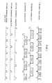
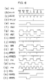
- Fig. 1 is a timing chart showing conditions of signals in a video signal recording-reproduction device.
- Fig. 2 is a block diagram showing a configuration of the video signal recording-reproduction device.
- Fig. 3 is a circuit diagram showing one portion of a line memory control circuit of a recording system.
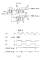
- Fig. 4 is a timing chart showing conditions of signals in the circuit shown in Fig. 3.
- Fig. 5 is a timing chart showing conditions of signals in the recording system.
- Fig. 6 is a block diagram showing the line memory control circuit.
- Fig. 7 is a circuit diagram of a field discrimination circuit.
- Fig. 8 is a timing chart showing conditions of signals in the field discrimination circuit.
- Fig. 9 is a timing chart showing conditions of signals in a frame clear pulse generation circuit and a selector pulse generation circuit.
- Fig. 10 is a circuit diagram of the frame clear pulse generation circuit and selector pulse generation circuit.
- Fig. 11 is a timing chart showing conditions of signals in the first and second line memory control circuits.
- Fig. 12 is a circuit diagram of the first and second line memory control circuits.
- Fig. 13 is a circuit diagram of a PLL circuit.
- Fig. 14 is a circuit diagram showing mutual connections of an A/D converter, line memories and D/A converters in the recording system.
- Fig. 15 is a block diagram showing a configuration of a line memory control circuit of reproduction system.
- Fig. 16 is a timing chart showing conditions of signals of the reproduction system.
- Fig. 17 is a circuit diagram showing mutual connections of a VD generation circuit, phase restoration means and a field discrimination circuit.
- Fig. 18 is a timing chart showing conditions of signals in the line memory control circuit of the reproduction system.
- Fig. 19 is a circuit diagram showing one portion of the line memory control circuit of the reproduction system.
- Fig. 20 is a circuit diagram showing one portion of the line memory control circuit of the reproduction system.
- Fig. 21 is a circuit diagram showing mutual connections of A/D converters, line memories and a D/A converter in the reproduction system.
- Fig. 22 is a block diagram showing another example of configuration of a video signal recording-reproduction device.
- Fig. 23 shows the prior art, and is a timing chart showing conditions of signals in a video signal recording-reproduction device.
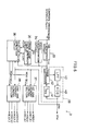
- the disclosure of the present invention is made with respect to a video signal recording-reproduction device which performs recording, and reproduces the recordings, for example, by the use of rotary head in the helical recording method.
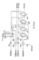
- the video signal recording-reproduction device includes a recording system for recording on a magnetic tape (recording medium) an input video signal as a record signal and a reproduction system for reproducing a record signal recorded on the magnetic tape as a reproduction video signal.
- the recording system comprises an A/D converter 1 for converting an input video signal as an analog signal into a digital signal and a sync separation circuit 2 for forming a sync separated signal corresponding to a horizontal synchronizing signal portion of the input video signal.
- the sync separation circuit 2 is connected to a line memory control circuit 3 as a phase changing means.
- the line memory control circuit 3 releases various reset pulses and clocks to respective line memories 4, 5 according to the sync separated signal from the sync separation circuit 2.
- the line memory control circuit 3 comprises, for example, FF (Flip-Flop) circuits 3a, 3b, 3c, 3d, 3e and NAND circuits 3f, 3g, as shown in Fig. 3, and is arranged to release a reset pulse 1 (Fig. 4 e) and a reset pulse 2 (Fig. 4 f) based on an HD signal (Fig. 4 a) whose one cycle coincides with one horizontal scanning period (hereinafter referred to as H) and on a clock (Fig. 4 b).
- the reset pulses 1, 2 are entered to the line memories 4, 5 respectively.
- the above-mentioned A/D converter 1 is connected to the line memories 4, 5, and thereby an input video signal converted into a digital signal is entered thereto from the A/D converter 1. Then, the line memories 4, 5 conduct time base extension on the input video signal and separate it into two channels according to the reset pulses and clocks from the line memory control circuit 3, thereby releasing divided signals with a phase shift of 1/2H to each other.
- the signals derived from the input video signal, separated into two channels by the line memories 4, 5, are converted into record signals in two lines of the signal recording systems.
- the signal recording system includes the line memories 4, 5, D/A converters 6, 7 for converting a digital signal into an analog signal, modulators 8, 9 and recording amplifiers 10, 11 for predetermined voltage amplification.
- the record signals formed in the signal recording systems are recorded on a magnetic tape (not shown) in two channels with a phase shift of 1/2H to each other through heads 12, 13.
- the reproduction system is connected to the heads 12, 13, and the record signals with a phase shift of 1/2H to each other are reproduced through the heads 12, 13.
- the heads 12, 13 are connected to respective reproduction amplifiers 14, 15 for amplifying the reproduced signals, and the reproduction amplifiers 14, 15 are connected to respective demodulators 16, 17 for converting frequency into voltage.
- the demodulators 16, 17 are on the one hand connected to A/D converters 18, 19 for converting analog signal into digital signal, and on the other hand, connected to a sync separation circuit 22 for extracting sync separated signals, each forming a horizontal synchronizing signal portion, from respective record signals. Further, the sync separation circuit 22 is connected to a line memory control circuit 23 including a phase restoration means for conducting logical add of the sync separated signals. With the arrangement, the line memory control circuit 23 can generate a horizontal synchronizing signal with a frequency identical to that of the input video signal.
- the line memory control circuit 23 is connected to line memories 20, 21 to which are connected the respective A/D converters 18, 19, whereby the record signals converted into digital signals are entered to the line memories 20, 21.
- the line memories 20, 21 conduct time compression of the record signals entered thereto, based on signals released from the line memory control circuit 23.
- the reproduction amplifiers 14, 15, demodulators 16, 17, A/D converters 18, 19 and line memories 20, 21 pertain to the signal reproduction system.
- the line memories 20, 21 are connected to a D/A converter 25 through a switch 24.
- the switch 24 on the one hand permits continuity of the line memory 20 and D/A converter 25 with every odd numbered H, and on the other hand, permits continuity of the line memory 21 and D/A converter 25 with every even numbered H.
- the D/A converter 25 releases an output video signal by converting outputs from the line memories 20, 21 into analog signals.
- An input video signal (Fig. 1 a) is entered to the A/D converter 1 to be converted into a digital signal, and at the same time entered to the sync separation circuit 2, which conducts sync separation on the input video signal.
- a sync separated signal obtained by the sync separation makes a reference signal for time base extension, and is entered to the line memory control circuit 3.
- the line memory control circuit 3 generates various signals for controlling the line memories based on the sync separated signal.
- the input video signal which has been converted into a digital signal in the A/D converter 1 is entered to the line memory 4, 5, where the signal is divided into two channels and subject to time base extension, thereby forming record signals (Figs. 1 b, c) with a phase shift of 1/2H to each other.
- An output of the line memory 4 forming the CH1 is entered to the D/A converter 6 to be converted into an analog signal, while an output of the line memory 5 forming the CH2 is entered to the D/A converter 7 to be converted into an analog signal.
- the record signals (Figs. 1 b, c) are entered to the respective modulators 8, 9 where they are frequency modulated, and then amplified by the recording amplifiers 10, 11, thereby being recorded on a magnetic tape in two channels through the magnetic beads 12, 13.
- the record signals (FM modulated signals of Figs. 1 b, c) recorded on the magnetic tape, after having been reproduced through the heads 12, 13 with a phase shift of 1/2H to each other, are entered to the reproduction amplifiers 14, 15.
- the record signals (FM modulated signals of Figs. 1 b, c) amplified by the reproduction amplifiers 14, 15, after having been demodulated in the demodulators 16, 17, are converted into digital signals in the A/D converters 18, 19.
- the record signals converted into digital signals (digital signals of Figs. 1 b, c) are entered to the line memories 20, 21 respectively.
- a sync separated signal (Fig. 1 d) of the CH1 and a sync separated signal (Fig. 1 e) of the CH2 are extracted from the respective record signals (Figs. 1 b, c) demodulated in the demodulators 16, 17.
- These sync separated signals (Figs. 1 d, e) are entered to the line memory control circuit 23.
- logical add is carried out on the sync separated signals (Figs. 1 d, e) with a phase shift of 1/2H to each other, and a sync separated signal (Figs. 1 f) identical to that of the input video signal (Fig. 1 a) is formed.
- the sync separated signal (Fig. 1 f) is entered to line memories 20, 21 as a reference signal for time compression.
- the line memories 20, 21 conduct time compression of the record signals (Figs. 1 b, c) according to the sync separated signal (Fig. 1 f).
- the record signals are subject to time compression while the switch 24 is changing its selection so that the line memory 20 is selected with every odd numbered H, and the line memory 21 is selected with every even numbered H.
- the video signal recording-reproduction device is arranged such that, in recording an input video signal (Fig. 1 a) on a magnetic tape, it can record a record signal (Fig. 1 b) of CH1 and a record signal (Fig. 1 c) of CH2, with a phase shift of 1/2H to each other while, in reproduction, it can obtain a sync separated signal (Fig. 1 f) having an identical phase to that of the input video signal (Fig. 1 a) by conducting logical add of sync separated signals (Figs. 1 d, e) obtained from the record signals (Figs. 1 b, c).
- the video signal recording-reproduction device having the sync separated signal (Fig. 1 f) as a reference signal, requires no frequency doubler or the like for permitting conformity to the phase of the input video signal (Fig. 1 a), and thereby it is possible to simplify the circuit for reproducing the divided record signals (Figs. 1 b, c) to form the input video signal (Fig. 1 a) before having been divided.
- the record signal may be subject to time base extension of N-times (for example, triple or quadruple), and may be divided into channels the number of which is given by N or integral multiples of N (for example, three channels or four channels) to be recorded or reproduced.
- N-times for example, triple or quadruple
- N integral multiples of N
- a record signal for each channel may be recorded with a phase shift of 1/N horizontal scanning period (H) to one another, and in reproduction, by conducting logical add of sync separated signals of those channels, it is possible to simplify the circuit.
- H horizontal scanning period
- the line memory control circuit 3 to which a composite synchronizing signal (Fig. 5 a) is entered from the sync separation circuit 2 of Fig. 2, comprises an HD generation circuit 33 for releasing the HD signal (Fig. 5 b) based on the composite synchronizing signal (Fig. 5 a), as is shown in Fig. 6.
- An output of the HD generation circuit 33 is connected to a PLL circuit 39 for forming an fsc signal as a reference clock, to a field discrimination circuit 34 to which the composite synchronizing signal (Fig. 5 a) is entered as in the case of the HD generation circuit 33, and to a selector pulse generation circuit 36.
- the field discrimination circuit 34 conducts vertical sync separation and field discrimination from the composite synchronizing signal (Fig. 5 a), and an FD (Field Discrimination) signal (Fig. 5 d) released from the field discrimination circuit 34 is entered to a frame clear pulse generation circuit 35.
- the frame clear pulse generation circuit 35 forms an FCLR1 signal and an FCLR2 signal, which will be described later, each having a different phase to each other and released therefrom only once every one frame, and releases those signals to the selector pulse generation circuit 36.
- the selector pulse generation circuit 36 is arranged to form an SEL1 signal (Fig. 5 f) for selecting every odd numbered H and an SEL2 signal (Fig. 5 e) for selecting every even numbered H, and the SEL1 signal (Fig. 5 f) is released to a first line memory control section 37 of the channel 1 side, while the SEL2 signal (Fig. 5 e) is released to a second line memory control section 38 of the channel 2 side.
- the first line memory control section 37 is arranged such that it can release to the line memory 4 of Fig. 2, a WRES1 signal (Fig. 5 g) indicating a start point for writing, a WCLK1 signal as a clock for writing, an RRES1 signal (Fig. 5 i) indicating a start point for reading, and an RCLK1 signal as a clock for reading.
- the second line memory control section 38 is arranged such that it can release to the line memory 5 of Fig. 2, a WRES2 signal (Fig. 5 h) indicating a start point for writing, a WCLK2 signal as a clock for writing, an RRES2 signal (Fig. 5 j) indicating a start point for reading, and an RCLK2 signal as a clock for reading.
- the field discrimination circuit 34 for discriminating between odd numbered fields and even numbered fields comprises, for example, monostable multivibrators 100, 102 of 4538 or the like and FF (Flip-Flop) circuits 101, 103 of HC74 or the like, as is shown in Fig. 7.
- a composite synchronizing signal (Fig. 8 a) is entered to the monostable multivibrator 100 through an A terminal (trigger input terminal) thereof.
- the monostable multivibrator 100 is provided with a resistor 100a of 100k ⁇ and a capacitor 100b of 100pF, and the resistor 100a and the capacitor 100b are thus arranged to set pulse width of an MSync signal (Fig. 8 c) which is released upon receiving a falling edge of the composite synchronizing signal (Fig. 8 a).
- the composite synchronizing signal (Fig. 8 a) is also entered to a D-terminal of the FF circuit 101 to which the MSync signal (Fig. 8 c) is entered through a clock terminal thereof.
- the FF circuit 101 on one hand releases a VD signal (Fig. 8 d) from a Q-terminal thereof, and on the other hand releases an inverted VD signal (Fig. 8 e) from a Q -terminal thereof.
- the Q -terminal of the FF circuit 101 is connected to a B-terminal (trigger input terminal) of the monostable multivibrator 102, which is provided with a variable resistor 102a of 68k ⁇ , a resistor 102b of 150k ⁇ and a capacitor 102c of 100pF.
- Those variable resistor 102a, resistor 102b and capacitor 102c are arranged to set pulse width of an SVD signal (Fig. 8 f) which is released from the Q -terminal upon receiving a falling edge of the VD signal (Fig. 8 e).
- the Q -terminal of the monostable multivibrator 102 is connected to a clock terminal of the FF circuit 103, and the HD signal (Fig. 8 b) is entered to a D-terminal of the FF circuit 103.
- the FF circuit 103 releases an FD signal (Fig. 8 g) from a Q-terminal thereof, which signal is set low with every odd numbered field, and set high with every even numbered field, based on the HD signal (Fig. 8 b) and the SVD signal (Fig. 8 f).
- An output of the above-mentioned field discrimination circuit 34 is connected to the frame clear pulse generation circuit 35, as is shown in Fig. 6, and the frame clear pulse generation circuit 35 is connected to the selector pulse generation circuit 36, and thereby arranged to release an FCLR1 signal and an FCLR2 signal.
- the frame clear pulse generation circuit 35 and selector pulse generation circuit 36 possess a circuit configuration shown in Fig. 10.
- the frame clear pulse generation circuit 35 includes a monostable multivibrator 104 to which the HD signal (Fig. 9 b) is entered, and the monostable multivibrator 104 releases a LHD signal (Fig. 9 c) with its pulse width predeterminately set.
- a Q -terminal of the monostable multivibrator 104 is connected to respective clock terminals of FF circuits 105, 106, and a Q-terminal of the FF circuit 105 is connected to a D-terminal (data terminal) of the FF circuit 106. Further, an output terminal of a NAND circuit 107 with 4 inputs is connected to a D-terminal of the FF circuit 105, and to each of the inputs of the NAND circuit 107, are respectively connected a Q1 terminal, Q2 terminal, Q4 terminal and Q10 terminal (all are output terminals) of a counter circuit 108 of HC4040 or the like.
- an output terminal of a NOT circuit 109 is connected to a CLK terminal of the counter circuit 108, and the HD signal (Fig. 9 b) is entered to an input terminal of the NOT circuit 109.
- an output terminal of a NOT circuit 110 is connected to an RES terminal of the counter circuit 108, and to an input terminal of the NOT circuit 110, is connected an output terminal of a 2-input NAND circuit 111, which releases the FCLR1 signal (Fig. 9 e) which will be described later.
- the FF circuits 105, 106 respectively release an MSK1 signal (Fig. 9 g) and an MSK2 signal (Fig. 9 h) for resetting the respective WRES signals at their pulse indicating the number 525H.
- a Q -terminal of an FF circuit 112 To respective input terminals of the NAND circuit 111, are connected a Q -terminal of an FF circuit 112 and a Q-terminal of an FF circuit 113.
- a Q-terminal of the FF circuit 112 is connected to a D-terminal of the FF circuit 113, and the FD signal (Fig. 9 a) is entered to a D-terminal of the FF circuit 112.
- a 4fsc signal is entered to respective clock terminals of the FF circuits 112, 113.
- the NAND circuit 111 can release the inverted FCLR1 signal (Fig. 9 e) having pulse width corresponding to one cycle of the 4fsc signal from a falling edge of the FD signal (Fig. 9 a).
- the 4fsc signal which is entered to the clock terminals of the FF circuits 112, 113, is also fed to respective clock terminals of FF circuits 114, 115.
- the FF circuit 114 whose D-terminal is connected to a Q-terminal of the FF circuit 106, has its Q-terminal connected to a D-terminal of the FF circuit 115.
- the Q -terminal of the FF circuit 114 is connected to one of input terminals of a 2-input NAND circuit 116, and a Q-terminal of the FF circuit 115 is connected to the other input terminal of the NAND circuit 116.
- the NAND circuit 116 can release the inverted FCLR2 signal (Fig. 9 i) with phase lead of substantial 1H to the FCLR1 signal.
- FCLR 1 signal (Fig. 9 e) and the FCLR2 signal (Fig. 9 i), which are released from the respective NAND circuits 111, 116 with inverted phase, is arranged to produce a pulse once every one frame, and thereby the FCLR1 signal (Fig. 9 e) produces a pulse at every number 1H forming a leading portion of a frame, while the FCLR2 signal (Fig.9 i) produces a pulse at every number 525H forming a rear end portion of a frame.
- the FCLR1 signal (Fig. 9 e) and the FCLR2 signal (Fig. 9 i) are released to the selector pulse generation circuit 36.
- the selector pulse generation circuit 36 includes an FF circuit 117 having a CLR terminal to which the FCLR1 signal (Fig. 9 e) is entered and an FF circuit 118 having a CLR terminal to which the FCLR2 signal (Fig. 9 i) is entered, and those FF circuits 117, 118 which are connected to each other through respective D-terminal and Q -terminal, have the HD signal (Fig. 9 b) entered thereto through respective clock terminals.
- the FF circuit 117 can release the SEL2 signal (Fig. 9 f) for selecting every even numbered H while the FF circuit 118 can release the SEL1 signal (Fig. 9 j) for selecting every odd numbered H.
- the SEL1 signal (Fig. 9 j) and the MSK1 signal (Fig. 9 g) from the FF circuit 105 are fed to the first line memory control section 37, as is shown in Fig. 6.
- the SEL2 signal (Fig. 9 f) and the MSK2 signal (Fig. 9 h) from the FF circuit 106 of Fig. 10 are fed to the second line memory control section 38.
- Those control sections 37, 38 have the same circuit configuration, and a detailed explanation is given of the circuit configuration referring to Fig. 12.
- the first line control memory control section 37(38) has four stages of FF circuits 119 to 122, and the 4fsc signal (Fig. 11 a) is entered to each clock terminal of the FF circuits 119 to 122. Further, an SEL signal (Fig. 11 b), actually the SEL1 (SEL2) signal in this case, is entered to a D-terminal of the FF circuit 119 at the first stage, and a Q-terminal of the FE circuit 119 is connected to a D-terminal of the FF circuit 120 at the second stage.
- SEL signal Fig. 11 b
- a Q-terminal of the FF circuit 120 is connected to a D-terminal of the FE circuit 121 at the third stage, while a Q-terminal of the FE circuit 121 is connected to a D-terminal of the FE circuit 122 at the last stage.
- a Q -terminal of the FE circuit 122 is connected to one of input terminals of a 2-input NAND circuit 123, and a Q-terminal of the FE circuit 120 at the second stage is connected to the other input terminal of the NAND circuit 123.
- the NAND circuit 123 can release the inverted RRES signal (Fig. 11 f) having a pulse which appears immediately after one cycle of the 4fsc signal (Fig. 11 a) has expired since receipt of a rising edge of the SEL signal (Fig. 11 b) and whose width corresponds to 2 cycles of the 4fsc signal.
- each clock terminal of the FF circuits 119 to 122 is connected to two stages of NOT circuits 124, 125, and the NOT circuit 125 at the second stage releases the WCLK signal (Fig. 11 d) having a slight phase delay to the 4fsc signal (Fig. 11 a).
- a Q-terminal of the FF circuit 119 is connected to one of input terminals of a 2-input NAND circuit 127, and a Q -terminal of the FF circuit 120 is connected to the other input terminal of the NAND circuit 127.
- An output terminal of the NAND circuit 127 is connected to one of input terminals of an 2-input OR circuit 126, and to the other input terminal of the OR circuit 126 is entered an MSK signal, actually the MSK1 signal (MSK2 signal) from the selector pulse generation circuit 36 of Fig. 6.
- the OR circuit 126 releases the WRES signal (Fig. 11 c) having a pulse whose width corresponds to 1 cycle of the 4fsc signal from a rising edge of the SEL signal (Fig. 11 b).
- the output terminal of the NAND circuit 127 is also connected to an asynchronous clear-type dividing circuit 128 of HC163 or the like.
- the above-mentioned 4fsc signal (Fig. 11 a) is entered to a clock terminal of the asynchronous clear-type dividing circuit 128.
- the asynchronous clear-type dividing circuit 128 is thus arranged to release the inverted RCLK signal (Fig. 11 g) having a frequency corresponding to 1/2 of that of the 4fsc signal, through a NOT circuit 129.
- the WCLK signal (Fig. 11 d) having the same frequency as the 4fsc signal in writing data and to conduct time base extension of double in reading data by utilizing the RCLK signal (Fig. 11 g) having a frequency corresponding to 1/2 of that of the 4fsc signal.
- the PLL circuit 39 comprises a VCO (Voltage Control Oscillator) 40 of, for example, LS624 or the like, three 1/910 counters 41 each composed of, for example, HC161, a phase comparator 42 of, for example, MC4044 or the like and a LPF (Low Pass Filter) 43 composed of resistors and capacitors, as is shown in Fig. 13.
- VCO Voltage Control Oscillator
- 1/910 counters 41 each composed of, for example, HC161
- a phase comparator 42 of, for example, MC4044 or the like
- LPF Low Pass Filter
- the VCO 40 is connected to each of the three 1/910 counters 41, and thereby permitted to release the 4fsc signal.
- the 1/910 counters 41 to which the 4fsc signal is entered release a signal whose frequency is divided into 1/910 of that of the 4fsc signal, and which is fed to the phase comparator 42.
- To the phase comparator 42 is connected the HD generation circuit 33 for releasing the HD signal to be compared with the signal from the 1/910 counters 41.
- the phase comparator 42 compares the signal from the 1/910 counters 41 with the HD signal and thereby releases a phase error signal, which is fed to the VCO 40 through the LPF 43.
- the VCO 40 is permitted to release the 4fsc signal which has the same phase as the HD signal and forms a reference clock of 14.318 MHz which is 910 times that of the HD signal in the case of a signal in NTSC system, by being controlled in the LPF 43 so as to extract a dc component of the phase error signal and correct phase errors.
- the A/D converter 1 which is made of, for example, MB40578 or the like, converts an input video signal of 3V to 5V entered thereto through the V in terminal into a digital signal of 8 bits.
- the A/D converter 1 has terminals releasing the digital signal, connected to the line memories 4, 5 of, for example, HM63021 or the like through a latch circuit 130 of, for example, F574 or AC574.
- the line memories 4, 5 are respectively connected to the D/A converters 6, 7 of, for example, MB40778 or the like, and those D/A converters 6, 7 convert the digital signals from the line memories 4, 5 into analog signals, and thereby release those analog signals as record signals of CH1 and CH2.
- the composite synchronizing signals (Figs. 16 a, e) of the CH1 and CH2 are entered to the line memory control circuit 23 of the reproduction system from the sync separation circuit 22.
- Those composite synchronizing signals (Figs. 16 a, e) are entered to an OR circuit 44 as phase restoration means of the line memory control circuit 23.
- the OR circuit 44 forms a Mix C-Sync signal (Fig. 16 i) as a composite signal which is obtained by conducting logical add of the composite synchronizing signals (Figs. 16 a, e) of the CH1 and CH2, and thereby releases the Mix C-Sync signal to a monostable multivibrator 48.
- the monostable multivibrator 48 forms a MIX HD signal (Fig. 16 j) whose pulse width is made constant, and releases the MIX HD signal to a line memory control section 49 and a PLL circuit 50 for forming the 4fsc signal and the 2fsc signal.
- the composite synchronizing signals (Figs. 16 a, e) of the CH1 and CH2 are also entered to VD generation circuits 45, 46.
- the VD generation circuits 45, 46 respectively form VD signals (Figs. 16 c, g) of the CH1 and CH2 so as to feed them to a field discrimination circuit 47.
- the field discrimination circuit 47 releases an RFD signal (Fig. 16 h) obtained by conducting field discrimination, to the line memory control section 49.
- the line memory control section 49 releases signals for controlling the line memories 20, 21 of Fig. 2, for example, an OE1 signal and an OE2 signal which permit outputs of the line memories 20, 21 to become high impedance with their high level, and permit data from the line memories 20, 21 to be released with their low level, based on the RFD signal (Fig. 16 h), MIX HD signal (Fig. 16 j), 4fsc signal and 2fsc signal, each entered thereto.
- the VD generation circuit 45(46) of the line memory control circuit 23 comprises two stages of NOT circuits 133, 134(135, 136), a monostable multivibrator 137(138) whose A terminal is connected to an output terminal of the NOT circuit 134(136) at the second stage and an FF circuit 139(140) whose clock terminal is connected a Q-terminal of the monostable multivibrator 137(138) and whose D-terminal is connected to an output terminal of the NOT circuit 134(136).
- the FF circuits 139, 140 can release VD signals (Figs. 16 c, g) of the CH1 and CH2 from the Q-terminals thereof.
- the VD signals (Figs. 16 c, g) are entered to the field discrimination circuit 47, which includes a monostable multivibrator 141 and an FF circuit 142.
- the monostable multivibrator 141 whereto the VD signal (Fig. 16 c) of the CH1 is entered through an A terminal thereof, is connected to a clock terminal of the FF circuit 142 through a Q -terminal thereof.
- the monostable multivibrator 141 is arranged to release an inverted SVD signal (Fig. 16 d) of the CH1 to the FF circuit 142 from the Q -terminal.
- the FF circuit 142 to which the SVD signal (Fig. 16 d) is entered has a D-terminal to which the VD signal (Fig. 16 g) of the CH2 is entered, and based on the VD signal (Fig. 16 g) and the SVD signal (Fig. 16 d), releases the RFD signal (Fig. 16 h).
- the NOT circuits 133, 135 respectively situated at the first stage of the VD generation circuits 45, 46 have their output terminals respectively connected to input terminals of the 2-input OR circuit 44.
- the OR circuit 44 is thus arranged to release a Mix C-Sync signal (Fig. 16 i) obtained by conducting logical add of the composite synchronizing signals (Figs. 16 a, e) of the CH1 and CH2.
- An output terminal of the OR circuit 44 is connected to an A terminal of the monostable multivibrator 48, which releases a MixHD signal (Fig. 16 j) with a predetermined pulse width according to the Mix C-Sync signal (Fig. 16 i) entered thereto.
- the MixHD signal (Fig. 16 j) and the RFD signal (Fig. 16 h) from the field discrimination circuit 47 are released to the line memory control section 49, as is shown in Fig. 15, and to the line memory control section 49 is connected the PLL circuit 50 for releasing the 4fsc signal and 2fsc signal thereto.
- the line memory control section 49 includes a NOT circuit 143 to which the MixHD signal (Fig. 18 b) is entered and FF circuits 145, 146, and the NOT circuit 143 is connected to a clock terminal of a counter circuit 147 of HC4040 or the like.
- the counter circuit 147 has its RES terminal connected to an output terminal of the NOT circuit 144, with its Q1, Q2, Q4 and Q10 terminals connected to respective 4 inputs of a NAND circuit 148.
- the NAND circuit 148 is connected to a D-terminal of the FF circuit 145.
- the MixHD signal (Fig. 18 b) is entered to a clock terminal of the FF circuit 145.
- the FF circuit 145 is permitted to release an RMSK signal (Fig. 18 e) from a Q -terminal thereof based on the signal from the NAND circuit 148 and the MixHD signal (Fig. 18 b).
- the FF circuit 145 has its Q -terminal connected to one of input terminals of a 2-input NOR circuit 149. To the other input terminal of the NOR circuit 149 is connected a Q-terminal of the FF circuit 146 for releasing the RSEL signal (Fig. 18 g) thereto.
- the NOR circuit 149 is permitted to release on the one hand, an OE1 signal (Fig. 18 1) based on the RSEL signal (Fig. 18 g) and the RMSK signal (Fig. 18 e), and on the other hand, an OE2 signal (Fig. 18 k) through an NOR circuit 150.
- the RFD signal (Fig. 18 a) from the field discrimination circuit 47 is fed to a D-terminal of the FF circuit 153.
- the 2fsc signal (Fig. 18 o) from the PLL circuit 50 is fed to a clock terminal of the FF circuit 153.
- the FF circuit 153 has its Q-terminal connected to a D-terminal of an FF circuit 154, while its Q -terminal is connected to one of input terminals of a 2-input NAND circuit 152 which is connected to the NOT circuit 144.
- a Q-terminal of the FF circuit 154 is connected to the other input terminal of the NAND circuit 152.
- the 2fsc signal (Fig. 18 o) is entered to a clock terminal of the FF circuit 154.
- the 2fsc signal (Fig. 18 o) is also entered to clock terminals of respective FF circuits 156, 157.
- Those FF circuits 156, 157 are connected to each other through a Q-terminal of the FF circuit 156 and a D-terminal of the FF circuit 157, and the NOT circuit 143 is connected to a D-terminal of the FF circuit 156, thereby permitting an inverted MixHD signal (Fig. 18 c) to be entered thereto.
- a Q -terminal of the FF circuit 145 is connected to a CLR terminal of the FF circuit 156, and the RMSK signal (Fig. 18 e) from the Q -terminal is thus entered thereto.
- a Q-terminal of the FF circuit 156 is connected not only to the D-terminal of the FF circuit 157, but to one of input terminals of the 2-input NAND circuit 151, and to the other input terminal of the NAND circuit 151, is connected a Q -terminal of the FF circuit 157.
- the FF circuit 157 which is connected to a CLR terminal of the FF circuit 146 through the NAND circuit 151, is permitted to release an inverted VRes signal (Fig. 18 f) to the CLR terminal thereof.
- the FF circuits 158, 159 are connected to each other through a Q-terminal of the FF circuit 158 and a D-terminal of the FF circuit 159, and to a D-terminal of the FF circuit 158, is connected a Q-terminal of the FF circuit 146, thereby permitting the RSEL signal (Fig. 18 g) to be entered thereto.
- the Q-terminal and D-terminal of the FF circuits 158, 159 which are connected to each other, are also connected to one of input terminals of a 2-input NAND circuit 160.
- a Q -terminal of the FF circuit 159 is connected to the other input terminal of the NAND circuit 160, which is thus arranged to release an inverted RWRES signal (Fig. 18 i) through an OR circuit 161 of LS32 or the like with one of its input terminals connected to ground.
- FF circuits 162, 163, whereto the 2fsc signal (Fig. 18 o) is entered as in the case of the FF circuits 153, 154, are connected to each other through a Q-terminal of the FF circuit 162 and a D-terminal of the FF circuit 163, and a D-terminal of the FF circuit 146 is connected to a D-terminal of the FF circuit 162, thereby permitting the inverted RSEL signal (Fig. 18 h) to be entered thereto.
- the Q-terminal and D-terminal of the FF circuit 162, 163 which are connected to each other are also connected to one of input terminals of a 2-input NAND circuit 164.
- a Q -terminal of the FF circuit 163 is connected to the other input terminal of the NAND circuit 164, and an output of the NAND circuit 164 is connected to one of inputs of an OR circuit 165 of LS32 or the like.
- a Q -terminal of the FF circuit 145 is connected to the other input of the OR circuit 165.
- the OR circuit 165 thus releases an RWRES2 signal (Fig. 18 j) through the output thereof.
- a Q -terminal of the FF circuit 167 is connected to the other input terminal of the NAND circuit 168.
- the NAND circuit 168 is thus arranged to release an inverted RRRES1 signal (Fig. 18 m) through an OR circuit 169 of LS32 or the like.
- To a clock terminal of the FF circuit 170 is entered the 4fsc signal (Fig. 18 q) from the PLL circuit 50 of Fig. 15.
- a Q-terminal of the FF circuit 170 is on the one hand connected to a D-terminal of an FF circuit 171 whereto the 4fsc signal (Fig. 18 q) is entered through a clock terminal thereof, and on the other hand connected to one of input terminals of a 2-input NAND circuit 172.
- a Q -terminal of the FF circuit 171 is connected to the other input terminal of the NAND circuit 172.
- An output of the NAND circuit 172 is connected to one of input terminals of an OR circuit 173 of LS32 or the like.
- the RMSK signal (Fig. 18 e) from the FF circuit 145 of Fig. 19 is entered to the other input terminal of the OR circuit 173.
- the OR circuit 173 is thus arranged to release an inverted RRRES2 signal (Fig. 18 n).
- HM 63021s are used for line memories 20, 21, and the OE1 signal, 4fsc signal, RRRES1 signal and other signals from the line memory control circuit 23 are entered to one of the line memories, 20. Further, the OE2 signal, 4fsc signal, RRRES2 signal and other signals from the line memory control circuit 23 are entered to the other line memory 21.
- Outputs of those line memories 20, 21 are connected to the D/A converter 25 of MB40778 or the like, and thereby the D/A converter 25 is arranged to convert the digital signals from the line memories 20, 21 into analog signals so as to form and release an output video signal.
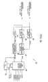
- the video signal recording-reproduction device of the present embodiment is provided with line memories 4, 5, 20, 21 and line memory control circuits 3, 23 separately disposed at the respective recording system and reproduction system; yet the device of the present invention is not limited to the arrangement, and, as shown in Fig. 22, may comprise the line memories 26, 27 for CH1 and CH2 for use in both the recording system and the reproduction system as well as the line memory control circuit 28 for controlling the line memories 26, 27 in recording as well as in reproduction.
- the line memory control circuit 28 controls switches 29, 30, 31, 32 (switching means) connected to the input and output terminals of the line memories 26, 27.
- the switches 29 to 32 are switched to the side a , and the signal from the A/D converter 1 is entered to the line memories 26, 27, and is released to the D/A converters 6, 7 after having been subject to time base extension by control of the line memory control circuit 28.
- the switches 29 to 32 are switched to the side b , and the signals from the A/D converters 18, 19 are entered to the respective line memories 26, 27, and are released to the D/A converter 25 after having been subject to time base compression by control of the line memory control circuit 28.
- a video signal recording-reproduction device in accordance with the present invention is provided with a recording system comprising phase changing means for shifting a phase of the record signal of each channel by a 1/N horizontal scanning period, and also provided with a recording system comprising phase restoration means for conducting logical add of the sync separated signals of the record signal, each reproduced from each channel.
- the record signal of each channel is recorded on the recording medium with a phase shift of a 1/N horizontal scanning period, and in reproduction, sync separated signals obtained from respective signals reproduced with the above state are subject to logical add by the phase restoration means.
- a sync separated signal obtained by conducting the logical add coincides with the horizontal synchronizing signal of the input video signal.
- the video signal recording-reproduction device permits conformity between a sync separated signal derived from record signals and a horizontal synchronizing signal of an input video signal, which is needed for converting divided record signals into an output video signal, solely by using the phase restoration means for conducting logical add, and thereby a simplified circuit configuration can be achieved.
Abstract
Description
- The present invention relates to a video signal recording-reproduction device for recording and reproducing a video signal with wideband for use in, for example, HDTV (High Definition Television) VTRs (Video Tape Recorders) and the like.
- In the case of recording a video signal with wideband on a recording medium such as a magnetic tape, an input video signal (Fig. 23 a) is sometimes arranged to undergo time base extension of double by the use of time base conversion means, and are divided into two channels to be recorded or reproduced. In conventional video signal recording-reproduction devices, every odd numbered 1H (horizontal scanning period) of those divided video signals (Fig. 23 a) is made to form a record signal (Fig. 23 b) for channel 1 (CH1) while every even numbered 1H is made to form a record signal (Fig. 23 c) for channel 2 (CH2), and thereby those two signals are recorded with the same phase. On the other hand, in reproduction, the divided record signals of two channels (Figs. 23 b, c) are converted into the same signal as the input video signal before divided (Fig. 23 a), by conducting time base compression.
- However, the conventional video signal recording-reproduction devices present a problem that a complicated circuit configuration is needed for converting the divided record signals of two channels (Figs. 23 b, c) into the input video signal (Fig. 23 a) before divided in reproduction.
- More specifically, when the divided record signals (Figs. 23 b, c) undergo time base compression, sync separated signals (Figs. 23 d, e) corresponding to a horizontal synchronizing signal of the input video signal (Fig. 23 a) are used as reference signals. In this case, since these sync separated signals (Figs. 23 d, e) are formed by reproducing the record signals (Figs. 23 b, c) recorded with the same phase, they also have the same phase. Accordingly, when the sync separated signals (Figs. 23 d, e) are used as reference signals, a frequency doubler is necessary in order to conform the phase to that of the horizontal synchronizing signal which the input video signal (Fig. 23 a) possessed, thereby causing a complicated circuit configuration.
- It is an object of the present invention to provide a video signal recording-reproduction device which includes a simplified circuit for converting divided record signals into the same signal as the input video signal before divided.
- In order to achieve the above object, a video signal recording-reproduction device according to the present invention comprises a recording system wherein an input video signal is subject to time base extension of N-times to form a record signal, and the record signal is divided into channels the number of which is given by N or integral multiples of N to be recorded on a magnetic tape as a recording medium and a reproduction system wherein the record signals recorded in the recording medium are reproduced by each channel, and an output video signal is formed by conforming sync separated signals of the respective divided record signals to a horizontal synchronizing signal of the input video signal. The recording system includes phase changing means for shifting a phase of the record signal of each channel by a 1/N horizontal scanning period, while the reproduction system includes phase restoration means for conducting logical add of the sync separated signals of the record signals, each reproduced by each channel.
- With the above arrangement, the phase changing means of the recording system enables the phase of the record signal of each channel, recorded in the recording medium to shift by a 1/N horizontal scanning period. Accordingly, in reproduction, each record signal is reproduced with the phase of its sync separated signal shifted by a 1/N horizontal scanning period. Then, the phase restoration means conducts logical add of these sync separated signals. As a result, a sync separated signal obtained by conducting the logical add coincides with the horizontal synchronizing signals of the input video signal. Thus, the video signal recording-reproduction device permits conformity between a sync separated signal derived from record signals and a horizontal synchronizing signal of an input video signal, which is needed for converting divided record signals into an output video signal, solely by using the phase restoration means. Therefore, for example, no frequency doubler is necessary, and a simplified circuit configuration can be achieved.
- For a fuller understanding of the nature and advantages of the invention, reference should be made to the ensuing detailed description taken in conjunction with the accompanying drawings.
- Figs. 1 to 22 show one embodiment of the present invention.
- Fig. 1 is a timing chart showing conditions of signals in a video signal recording-reproduction device.
- Fig. 2 is a block diagram showing a configuration of the video signal recording-reproduction device.
- Fig. 3 is a circuit diagram showing one portion of a line memory control circuit of a recording system.
- Fig. 4 is a timing chart showing conditions of signals in the circuit shown in Fig. 3.
- Fig. 5 is a timing chart showing conditions of signals in the recording system.
- Fig. 6 is a block diagram showing the line memory control circuit.
- Fig. 7 is a circuit diagram of a field discrimination circuit.
- Fig. 8 is a timing chart showing conditions of signals in the field discrimination circuit.
- Fig. 9 is a timing chart showing conditions of signals in a frame clear pulse generation circuit and a selector pulse generation circuit.
- Fig. 10 is a circuit diagram of the frame clear pulse generation circuit and selector pulse generation circuit.
- Fig. 11 is a timing chart showing conditions of signals in the first and second line memory control circuits.
- Fig. 12 is a circuit diagram of the first and second line memory control circuits.
- Fig. 13 is a circuit diagram of a PLL circuit.
- Fig. 14 is a circuit diagram showing mutual connections of an A/D converter, line memories and D/A converters in the recording system.
- Fig. 15 is a block diagram showing a configuration of a line memory control circuit of reproduction system.
- Fig. 16 is a timing chart showing conditions of signals of the reproduction system.
- Fig. 17 is a circuit diagram showing mutual connections of a VD generation circuit, phase restoration means and a field discrimination circuit.
- Fig. 18 is a timing chart showing conditions of signals in the line memory control circuit of the reproduction system.
- Fig. 19 is a circuit diagram showing one portion of the line memory control circuit of the reproduction system.
- Fig. 20 is a circuit diagram showing one portion of the line memory control circuit of the reproduction system.
- Fig. 21 is a circuit diagram showing mutual connections of A/D converters, line memories and a D/A converter in the reproduction system.
- Fig. 22 is a block diagram showing another example of configuration of a video signal recording-reproduction device.
- Fig. 23 shows the prior art, and is a timing chart showing conditions of signals in a video signal recording-reproduction device.
- The following description will discuss one embodiment of the present invention referring to Figs. 1 to 22.
- The disclosure of the present invention is made with respect to a video signal recording-reproduction device which performs recording, and reproduces the recordings, for example, by the use of rotary head in the helical recording method. As shown in Fig. 2, the video signal recording-reproduction device includes a recording system for recording on a magnetic tape (recording medium) an input video signal as a record signal and a reproduction system for reproducing a record signal recorded on the magnetic tape as a reproduction video signal.
- The recording system comprises an A/
D converter 1 for converting an input video signal as an analog signal into a digital signal and async separation circuit 2 for forming a sync separated signal corresponding to a horizontal synchronizing signal portion of the input video signal. Thesync separation circuit 2 is connected to a linememory control circuit 3 as a phase changing means. The linememory control circuit 3 releases various reset pulses and clocks torespective line memories sync separation circuit 2. - In other words, the line
memory control circuit 3 comprises, for example, FF (Flip-Flop)circuits NAND circuits reset pulses line memories - As shown in Fig. 2, the above-mentioned A/
D converter 1 is connected to theline memories D converter 1. Then, theline memories memory control circuit 3, thereby releasing divided signals with a phase shift of 1/2H to each other. - The signals derived from the input video signal, separated into two channels by the
line memories line memories A converters modulators recording amplifiers heads - On the other hand, as with the recording system, the reproduction system is connected to the
heads heads heads respective reproduction amplifiers reproduction amplifiers respective demodulators - The
demodulators D converters sync separation circuit 22 for extracting sync separated signals, each forming a horizontal synchronizing signal portion, from respective record signals. Further, thesync separation circuit 22 is connected to a linememory control circuit 23 including a phase restoration means for conducting logical add of the sync separated signals. With the arrangement, the linememory control circuit 23 can generate a horizontal synchronizing signal with a frequency identical to that of the input video signal. - The line
memory control circuit 23 is connected to linememories D converters line memories line memories memory control circuit 23. As described above, thereproduction amplifiers demodulators D converters line memories - The
line memories A converter 25 through a switch 24. The switch 24 on the one hand permits continuity of theline memory 20 and D/A converter 25 with every odd numbered H, and on the other hand, permits continuity of theline memory 21 and D/A converter 25 with every even numbered H. The D/A converter 25 releases an output video signal by converting outputs from theline memories - The following description will discuss operation of a video signal recording-reproduction device having the above configuration.
- An input video signal (Fig. 1 a) is entered to the A/
D converter 1 to be converted into a digital signal, and at the same time entered to thesync separation circuit 2, which conducts sync separation on the input video signal. A sync separated signal obtained by the sync separation makes a reference signal for time base extension, and is entered to the linememory control circuit 3. The linememory control circuit 3 generates various signals for controlling the line memories based on the sync separated signal. - Moreover, the input video signal which has been converted into a digital signal in the A/
D converter 1, is entered to theline memory - An output of the
line memory 4 forming the CH1 is entered to the D/A converter 6 to be converted into an analog signal, while an output of theline memory 5 forming the CH2 is entered to the D/A converter 7 to be converted into an analog signal. The record signals (Figs. 1 b, c) are entered to therespective modulators recording amplifiers magnetic beads - On the other hand, the record signals (FM modulated signals of Figs. 1 b, c) recorded on the magnetic tape, after having been reproduced through the
heads reproduction amplifiers reproduction amplifiers demodulators D converters line memories - At this time, by the
sync separation circuit 22, a sync separated signal (Fig. 1 d) of the CH1 and a sync separated signal (Fig. 1 e) of the CH2 are extracted from the respective record signals (Figs. 1 b, c) demodulated in thedemodulators memory control circuit 23. Thus, logical add is carried out on the sync separated signals (Figs. 1 d, e) with a phase shift of 1/2H to each other, and a sync separated signal (Figs. 1 f) identical to that of the input video signal (Fig. 1 a) is formed. - The sync separated signal (Fig. 1 f) is entered to line
memories line memories line memory 20 is selected with every odd numbered H, and theline memory 21 is selected with every even numbered H. By entering to the D/A converter 25 the record signals having been subject to time compression, it is possible to obtain an output video signal identical to the input video signal (Fig. 1 a). - As explained above, the video signal recording-reproduction device is arranged such that, in recording an input video signal (Fig. 1 a) on a magnetic tape, it can record a record signal (Fig. 1 b) of CH1 and a record signal (Fig. 1 c) of CH2, with a phase shift of 1/2H to each other while, in reproduction, it can obtain a sync separated signal (Fig. 1 f) having an identical phase to that of the input video signal (Fig. 1 a) by conducting logical add of sync separated signals (Figs. 1 d, e) obtained from the record signals (Figs. 1 b, c).
- With the arrangement, the video signal recording-reproduction device having the sync separated signal (Fig. 1 f) as a reference signal, requires no frequency doubler or the like for permitting conformity to the phase of the input video signal (Fig. 1 a), and thereby it is possible to simplify the circuit for reproducing the divided record signals (Figs. 1 b, c) to form the input video signal (Fig. 1 a) before having been divided.
- Additionally, in the present embodiment, an example is shown wherein a record signal is subject to time base extension of double, and recording and reproduction are performed by the use of two channels; yet the present invention is not limited to the above arrangement. Therefore, the record signal may be subject to time base extension of N-times (for example, triple or quadruple), and may be divided into channels the number of which is given by N or integral multiples of N (for example, three channels or four channels) to be recorded or reproduced. In this case, a record signal for each channel may be recorded with a phase shift of 1/N horizontal scanning period (H) to one another, and in reproduction, by conducting logical add of sync separated signals of those channels, it is possible to simplify the circuit.
- Next, a detailed explanation will be given of the above-mentioned recording system and reproduction system.
- The line
memory control circuit 3 to which a composite synchronizing signal (Fig. 5 a) is entered from thesync separation circuit 2 of Fig. 2, comprises anHD generation circuit 33 for releasing the HD signal (Fig. 5 b) based on the composite synchronizing signal (Fig. 5 a), as is shown in Fig. 6. An output of theHD generation circuit 33 is connected to aPLL circuit 39 for forming an fsc signal as a reference clock, to afield discrimination circuit 34 to which the composite synchronizing signal (Fig. 5 a) is entered as in the case of theHD generation circuit 33, and to a selectorpulse generation circuit 36. - The
field discrimination circuit 34 conducts vertical sync separation and field discrimination from the composite synchronizing signal (Fig. 5 a), and an FD (Field Discrimination) signal (Fig. 5 d) released from thefield discrimination circuit 34 is entered to a frame clearpulse generation circuit 35. The frame clearpulse generation circuit 35 forms an FCLR1 signal and an FCLR2 signal, which will be described later, each having a different phase to each other and released therefrom only once every one frame, and releases those signals to the selectorpulse generation circuit 36. - The selector
pulse generation circuit 36 is arranged to form an SEL1 signal (Fig. 5 f) for selecting every odd numbered H and an SEL2 signal (Fig. 5 e) for selecting every even numbered H, and the SEL1 signal (Fig. 5 f) is released to a first linememory control section 37 of thechannel 1 side, while the SEL2 signal (Fig. 5 e) is released to a second linememory control section 38 of thechannel 2 side. - The first line
memory control section 37 is arranged such that it can release to theline memory 4 of Fig. 2, a WRES1 signal (Fig. 5 g) indicating a start point for writing, a WCLK1 signal as a clock for writing, an RRES1 signal (Fig. 5 i) indicating a start point for reading, and an RCLK1 signal as a clock for reading. On the other hand, the second linememory control section 38 is arranged such that it can release to theline memory 5 of Fig. 2, a WRES2 signal (Fig. 5 h) indicating a start point for writing, a WCLK2 signal as a clock for writing, an RRES2 signal (Fig. 5 j) indicating a start point for reading, and an RCLK2 signal as a clock for reading. - A detailed explanation will be given of each of the circuits composing the line
memory control circuit 3. - The
field discrimination circuit 34 for discriminating between odd numbered fields and even numbered fields comprises, for example,monostable multivibrators circuits monostable multivibrator 100 through an A terminal (trigger input terminal) thereof. Themonostable multivibrator 100 is provided with aresistor 100a of 100kΩ and acapacitor 100b of 100pF, and theresistor 100a and thecapacitor 100b are thus arranged to set pulse width of anMSync signal (Fig. 8 c) which is released upon receiving a falling edge of the composite synchronizing signal (Fig. 8 a). - Furthermore, the composite synchronizing signal (Fig. 8 a) is also entered to a D-terminal of the
FF circuit 101 to which the MSync signal (Fig. 8 c) is entered through a clock terminal thereof. TheFF circuit 101, on one hand releases a VD signal (Fig. 8 d) from a Q-terminal thereof, and on the other hand releases an invertedVD signal (Fig. 8 e) from aQ -terminal thereof. TheQ -terminal of theFF circuit 101 is connected to a B-terminal (trigger input terminal) of themonostable multivibrator 102, which is provided with avariable resistor 102a of 68kΩ, aresistor 102b of 150kΩ and acapacitor 102c of 100pF. Thosevariable resistor 102a,resistor 102b andcapacitor 102c are arranged to set pulse width of anSVD signal (Fig. 8 f) which is released from theQ -terminal upon receiving a falling edge of theVD signal (Fig. 8 e). - The
Q -terminal of themonostable multivibrator 102 is connected to a clock terminal of theFF circuit 103, and the HD signal (Fig. 8 b) is entered to a D-terminal of theFF circuit 103. With the arrangement, theFF circuit 103 releases an FD signal (Fig. 8 g) from a Q-terminal thereof, which signal is set low with every odd numbered field, and set high with every even numbered field, based on the HD signal (Fig. 8 b) and theSVD signal (Fig. 8 f). - An output of the above-mentioned
field discrimination circuit 34 is connected to the frame clearpulse generation circuit 35, as is shown in Fig. 6, and the frame clearpulse generation circuit 35 is connected to the selectorpulse generation circuit 36, and thereby arranged to release an FCLR1 signal and an FCLR2 signal. - The frame clear
pulse generation circuit 35 and selectorpulse generation circuit 36 possess a circuit configuration shown in Fig. 10. The frame clearpulse generation circuit 35 includes amonostable multivibrator 104 to which the HD signal (Fig. 9 b) is entered, and themonostable multivibrator 104 releases a LHD signal (Fig. 9 c) with its pulse width predeterminately set. - A
Q -terminal of themonostable multivibrator 104 is connected to respective clock terminals ofFF circuits FF circuit 105 is connected to a D-terminal (data terminal) of theFF circuit 106. Further, an output terminal of aNAND circuit 107 with 4 inputs is connected to a D-terminal of theFF circuit 105, and to each of the inputs of theNAND circuit 107, are respectively connected a Q₁ terminal, Q₂ terminal, Q₄ terminal and Q₁₀ terminal (all are output terminals) of acounter circuit 108 of HC4040 or the like. - Moreover, an output terminal of a
NOT circuit 109 is connected to a CLK terminal of thecounter circuit 108, and the HD signal (Fig. 9 b) is entered to an input terminal of theNOT circuit 109. Furthermore, an output terminal of aNOT circuit 110 is connected to an RES terminal of thecounter circuit 108, and to an input terminal of theNOT circuit 110, is connected an output terminal of a 2-input NAND circuit 111, which releases the FCLR1 signal (Fig. 9 e) which will be described later. With the arrangement, theFF circuits - To respective input terminals of the
NAND circuit 111, are connected aQ -terminal of anFF circuit 112 and a Q-terminal of anFF circuit 113. A Q-terminal of theFF circuit 112 is connected to a D-terminal of theFF circuit 113, and the FD signal (Fig. 9 a) is entered to a D-terminal of theFF circuit 112. Further, a 4fsc signal is entered to respective clock terminals of theFF circuits NAND circuit 111 can release the invertedFCLR1 signal (Fig. 9 e) having pulse width corresponding to one cycle of the 4fsc signal from a falling edge of the FD signal (Fig. 9 a). - The 4fsc signal which is entered to the clock terminals of the
FF circuits FF circuits FF circuit 114 whose D-terminal is connected to a Q-terminal of theFF circuit 106, has its Q-terminal connected to a D-terminal of theFF circuit 115. TheQ -terminal of theFF circuit 114 is connected to one of input terminals of a 2-input NAND circuit 116, and a Q-terminal of theFF circuit 115 is connected to the other input terminal of theNAND circuit 116. With the arrangement, theNAND circuit 116 can release the invertedFCLR2 signal (Fig. 9 i) with phase lead of substantial 1H to theFCLR1 signal. - Each of the
FCLR FCLR2 signal (Fig. 9 i), which are released from therespective NAND circuits FCLR1 signal (Fig. 9 e) produces a pulse at everynumber 1H forming a leading portion of a frame, while theFCLR2 signal (Fig.9 i) produces a pulse at every number 525H forming a rear end portion of a frame. - The
FCLR1 signal (Fig. 9 e) and theFCLR2 signal (Fig. 9 i) are released to the selectorpulse generation circuit 36. The selectorpulse generation circuit 36 includes anFF circuit 117 having a CLR terminal to which theFCLR1 signal (Fig. 9 e) is entered and anFF circuit 118 having a CLR terminal to which theFCLR2 signal (Fig. 9 i) is entered, and thoseFF circuits Q -terminal, have the HD signal (Fig. 9 b) entered thereto through respective clock terminals. With the arrangement, theFF circuit 117 can release the SEL2 signal (Fig. 9 f) for selecting every even numbered H while theFF circuit 118 can release the SEL1 signal (Fig. 9 j) for selecting every odd numbered H. - The SEL1 signal (Fig. 9 j) and the MSK1 signal (Fig. 9 g) from the
FF circuit 105 are fed to the first linememory control section 37, as is shown in Fig. 6. On the other hand, the SEL2 signal (Fig. 9 f) and the MSK2 signal (Fig. 9 h) from theFF circuit 106 of Fig. 10 are fed to the second linememory control section 38. Thosecontrol sections - The first line control memory control section 37(38) has four stages of
FF circuits 119 to 122, and the 4fsc signal (Fig. 11 a) is entered to each clock terminal of theFF circuits 119 to 122. Further, an SEL signal (Fig. 11 b), actually the SEL1 (SEL2) signal in this case, is entered to a D-terminal of theFF circuit 119 at the first stage, and a Q-terminal of theFE circuit 119 is connected to a D-terminal of theFF circuit 120 at the second stage. Moreover, a Q-terminal of theFF circuit 120 is connected to a D-terminal of theFE circuit 121 at the third stage, while a Q-terminal of theFE circuit 121 is connected to a D-terminal of theFE circuit 122 at the last stage. - A
Q -terminal of theFE circuit 122 is connected to one of input terminals of a 2-input NAND circuit 123, and a Q-terminal of theFE circuit 120 at the second stage is connected to the other input terminal of theNAND circuit 123. Thus, theNAND circuit 123 can release the invertedRRES signal (Fig. 11 f) having a pulse which appears immediately after one cycle of the 4fsc signal (Fig. 11 a) has expired since receipt of a rising edge of the SEL signal (Fig. 11 b) and whose width corresponds to 2 cycles of the 4fsc signal. - Moreover, each clock terminal of the
FF circuits 119 to 122 is connected to two stages ofNOT circuits NOT circuit 125 at the second stage releases theWCLK signal (Fig. 11 d) having a slight phase delay to the 4fsc signal (Fig. 11 a). Furthermore, a Q-terminal of theFF circuit 119 is connected to one of input terminals of a 2-input NAND circuit 127, and aQ -terminal of theFF circuit 120 is connected to the other input terminal of theNAND circuit 127. - An output terminal of the
NAND circuit 127 is connected to one of input terminals of an 2-input ORcircuit 126, and to the other input terminal of theOR circuit 126 is entered an MSK signal, actually the MSK1 signal (MSK2 signal) from the selectorpulse generation circuit 36 of Fig. 6. With the arrangement, theOR circuit 126 releases theWRES signal (Fig. 11 c) having a pulse whose width corresponds to 1 cycle of the 4fsc signal from a rising edge of the SEL signal (Fig. 11 b). - The output terminal of the
NAND circuit 127 is also connected to an asynchronous clear-type dividing circuit 128 of HC163 or the like. The above-mentioned 4fsc signal (Fig. 11 a) is entered to a clock terminal of the asynchronous clear-type dividing circuit 128. The asynchronous clear-type dividing circuit 128 is thus arranged to release the invertedRCLK signal (Fig. 11 g) having a frequency corresponding to 1/2 of that of the 4fsc signal, through aNOT circuit 129. With the arrangement, it is possible to use theWCLK signal (Fig. 11 d) having the same frequency as the 4fsc signal in writing data and to conduct time base extension of double in reading data by utilizing theRCLK signal (Fig. 11 g) having a frequency corresponding to 1/2 of that of the 4fsc signal. - Next, referring to Fig. 6, a detailed explanation will be given of the
PLL circuit 39 for forming the 4fsc signal to be entered to the first and second linememory control sections pulse generation circuit 35 and the selectorpulse generation circuit 36. - The
PLL circuit 39 comprises a VCO (Voltage Control Oscillator) 40 of, for example, LS624 or the like, three 1/910counters 41 each composed of, for example, HC161, aphase comparator 42 of, for example, MC4044 or the like and a LPF (Low Pass Filter) 43 composed of resistors and capacitors, as is shown in Fig. 13. - The
VCO 40 is connected to each of the three 1/910counters 41, and thereby permitted to release the 4fsc signal. The 1/910counters 41 to which the 4fsc signal is entered, release a signal whose frequency is divided into 1/910 of that of the 4fsc signal, and which is fed to thephase comparator 42. To thephase comparator 42, is connected theHD generation circuit 33 for releasing the HD signal to be compared with the signal from the 1/910 counters 41. - The
phase comparator 42 compares the signal from the 1/910counters 41 with the HD signal and thereby releases a phase error signal, which is fed to theVCO 40 through theLPF 43. Thus, theVCO 40 is permitted to release the 4fsc signal which has the same phase as the HD signal and forms a reference clock of 14.318 MHz which is 910 times that of the HD signal in the case of a signal in NTSC system, by being controlled in theLPF 43 so as to extract a dc component of the phase error signal and correct phase errors. - Next, referring to Fig. 2, a detailed explanation will be given of the
line memories memory control circuit 3 including the first and second linememory control sections D converter 1 and the D/A converters line memories - As shown in Fig. 14, the A/
D converter 1 which is made of, for example, MB40578 or the like, converts an input video signal of 3V to 5V entered thereto through the Vin terminal into a digital signal of 8 bits. The A/D converter 1 has terminals releasing the digital signal, connected to theline memories latch circuit 130 of, for example, F574 or AC574. - To one of the
line memories 4, are entered the 4fsc signal,RCLK1 signal,RRES1 signal andWRES1 signal, and theRCLK1 signal is released through aNOT circuit 132 as a 2fscCH1 signal. Further, to theother line memory 5, are entered the 4fsc signal,RCLK2 signal,RRES2 signal andWRES2 signal, and theRCLK2 signal is released through aNOT circuit 131 as 2fscCH2 signal. - The
line memories A converters A converters line memories - Additionally, as shown in Fig. 5, in order to form those record signals divided into respective two channels CH1 and CH2, it is necessary to divide data of the number 525H situated at the end into two of 1/2H so as to be apportioned to respective two channels. In that case, the data of the number 525H and data of the numbers 523H and 524H represent equalizing pulse portions of the video signal, i.e. they contain no information as picture images. Therefore, in the present embodiment, it is arranged that without storing the data of the number 525H in either
line memory - Next, the following description will discuss the reproduction system in detail.
- As shown in Fig. 15, the composite synchronizing signals (Figs. 16 a, e) of the CH1 and CH2 are entered to the line
memory control circuit 23 of the reproduction system from thesync separation circuit 22. Those composite synchronizing signals (Figs. 16 a, e) are entered to anOR circuit 44 as phase restoration means of the linememory control circuit 23. The ORcircuit 44 forms a Mix C-Sync signal (Fig. 16 i) as a composite signal which is obtained by conducting logical add of the composite synchronizing signals (Figs. 16 a, e) of the CH1 and CH2, and thereby releases the Mix C-Sync signal to amonostable multivibrator 48. Themonostable multivibrator 48 forms a MIX HD signal (Fig. 16 j) whose pulse width is made constant, and releases the MIX HD signal to a linememory control section 49 and aPLL circuit 50 for forming the 4fsc signal and the 2fsc signal. - Further, the composite synchronizing signals (Figs. 16 a, e) of the CH1 and CH2 are also entered to
VD generation circuits VD generation circuits field discrimination circuit 47. Thus, thefield discrimination circuit 47 releases an RFD signal (Fig. 16 h) obtained by conducting field discrimination, to the linememory control section 49. - The line
memory control section 49 releases signals for controlling theline memories line memories line memories - Next, a detailed explanation is given of the circuit configuration of the line
memory control circuit 23. - As shown in Fig. 17, the VD generation circuit 45(46) of the line
memory control circuit 23 comprises two stages ofNOT circuits 133, 134(135, 136), a monostable multivibrator 137(138) whose A terminal is connected to an output terminal of the NOT circuit 134(136) at the second stage and an FF circuit 139(140) whose clock terminal is connected a Q-terminal of the monostable multivibrator 137(138) and whose D-terminal is connected to an output terminal of the NOT circuit 134(136). With the arrangement, theFF circuits - The VD signals (Figs. 16 c, g) are entered to the
field discrimination circuit 47, which includes amonostable multivibrator 141 and anFF circuit 142. Themonostable multivibrator 141, whereto the VD signal (Fig. 16 c) of the CH1 is entered through an A terminal thereof, is connected to a clock terminal of theFF circuit 142 through aQ -terminal thereof. Thus, themonostable multivibrator 141 is arranged to release an invertedSVD signal (Fig. 16 d) of the CH1 to theFF circuit 142 from theQ -terminal. - The
FF circuit 142 to which theSVD signal (Fig. 16 d) is entered, has a D-terminal to which the VD signal (Fig. 16 g) of the CH2 is entered, and based on the VD signal (Fig. 16 g) and the SVD signal (Fig. 16 d), releases the RFD signal (Fig. 16 h). - Furthermore, the
NOT circuits VD generation circuits circuit 44. The ORcircuit 44 is thus arranged to release a Mix C-Sync signal (Fig. 16 i) obtained by conducting logical add of the composite synchronizing signals (Figs. 16 a, e) of the CH1 and CH2. An output terminal of theOR circuit 44 is connected to an A terminal of themonostable multivibrator 48, which releases a MixHD signal (Fig. 16 j) with a predetermined pulse width according to the Mix C-Sync signal (Fig. 16 i) entered thereto. - The MixHD signal (Fig. 16 j) and the RFD signal (Fig. 16 h) from the
field discrimination circuit 47 are released to the linememory control section 49, as is shown in Fig. 15, and to the linememory control section 49 is connected thePLL circuit 50 for releasing the 4fsc signal and 2fsc signal thereto. As shown in Fig. 19, the linememory control section 49 includes aNOT circuit 143 to which the MixHD signal (Fig. 18 b) is entered andFF circuits NOT circuit 143 is connected to a clock terminal of acounter circuit 147 of HC4040 or the like. - The
counter circuit 147 has its RES terminal connected to an output terminal of theNOT circuit 144, with its Q₁, Q₂, Q₄ and Q₁₀ terminals connected to respective 4 inputs of aNAND circuit 148. TheNAND circuit 148 is connected to a D-terminal of theFF circuit 145. The MixHD signal (Fig. 18 b) is entered to a clock terminal of theFF circuit 145. Thus, theFF circuit 145 is permitted to release an RMSK signal (Fig. 18 e) from aQ -terminal thereof based on the signal from theNAND circuit 148 and the MixHD signal (Fig. 18 b). - The
FF circuit 145 has itsQ -terminal connected to one of input terminals of a 2-input NORcircuit 149. To the other input terminal of the NORcircuit 149 is connected a Q-terminal of theFF circuit 146 for releasing the RSEL signal (Fig. 18 g) thereto. Thus, the NORcircuit 149 is permitted to release on the one hand, anOE1 signal (Fig. 18 1) based on the RSEL signal (Fig. 18 g) and the RMSK signal (Fig. 18 e), and on the other hand, anOE2 signal (Fig. 18 k) through an NORcircuit 150. - In the meantime, the RFD signal (Fig. 18 a) from the
field discrimination circuit 47 is fed to a D-terminal of theFF circuit 153. The 2fsc signal (Fig. 18 o) from thePLL circuit 50 is fed to a clock terminal of theFF circuit 153. TheFF circuit 153 has its Q-terminal connected to a D-terminal of anFF circuit 154, while itsQ -terminal is connected to one of input terminals of a 2-input NAND circuit 152 which is connected to theNOT circuit 144. On the other hand, a Q-terminal of theFF circuit 154 is connected to the other input terminal of theNAND circuit 152. - As in the case of the
FF circuit 153, the 2fsc signal (Fig. 18 o) is entered to a clock terminal of theFF circuit 154. The 2fsc signal (Fig. 18 o) is also entered to clock terminals ofrespective FF circuits FF circuits FF circuit 156 and a D-terminal of theFF circuit 157, and theNOT circuit 143 is connected to a D-terminal of theFF circuit 156, thereby permitting an invertedMixHD signal (Fig. 18 c) to be entered thereto. Further, aQ -terminal of theFF circuit 145 is connected to a CLR terminal of theFF circuit 156, and the RMSK signal (Fig. 18 e) from theQ -terminal is thus entered thereto. Moreover, a Q-terminal of theFF circuit 156 is connected not only to the D-terminal of theFF circuit 157, but to one of input terminals of the 2-input NAND circuit 151, and to the other input terminal of theNAND circuit 151, is connected aQ -terminal of theFF circuit 157. Thus, theFF circuit 157, which is connected to a CLR terminal of theFF circuit 146 through theNAND circuit 151, is permitted to release an invertedVRes signal (Fig. 18 f) to the CLR terminal thereof. - On the other hand, the 2fsc signal (Fig. 18 o) which is entered to the
FF circuits FF circuits 158, 159 for generating anRWRES1 signal (Fig. 18 i) and toFF circuits RWRES2 signal (Fig. 18 j). TheFF circuits 158, 159 are connected to each other through a Q-terminal of theFF circuit 158 and a D-terminal of the FF circuit 159, and to a D-terminal of theFF circuit 158, is connected a Q-terminal of theFF circuit 146, thereby permitting the RSEL signal (Fig. 18 g) to be entered thereto. - Further, the Q-terminal and D-terminal of the
FF circuits 158, 159 which are connected to each other, are also connected to one of input terminals of a 2-input NAND circuit 160. AQ -terminal of the FF circuit 159 is connected to the other input terminal of theNAND circuit 160, which is thus arranged to release an invertedRWRES signal (Fig. 18 i) through an ORcircuit 161 of LS32 or the like with one of its input terminals connected to ground. - On the other hand,
FF circuits FF circuits FF circuit 162 and a D-terminal of theFF circuit 163, and a D-terminal of theFF circuit 146 is connected to a D-terminal of theFF circuit 162, thereby permitting the invertedRSEL signal (Fig. 18 h) to be entered thereto. Further, the Q-terminal and D-terminal of theFF circuit input NAND circuit 164. AQ -terminal of theFF circuit 163 is connected to the other input terminal of theNAND circuit 164, and an output of theNAND circuit 164 is connected to one of inputs of an ORcircuit 165 of LS32 or the like. AQ -terminal of theFF circuit 145 is connected to the other input of theOR circuit 165. The ORcircuit 165 thus releases anRWRES2 signal (Fig. 18 j) through the output thereof. - The RSEL signal (Fig. 18 g) which is entered to the
FF circuit 158, is also entered to a D-terminal of theFF circuit 166 as is shown in Fig. 20, and the 4fsc signal (Fig. 18 g) from thePLL circuit 50 of Fig. 15 is entered to a clock terminal of theFF circuit 166. Moreover, a Q-terminal of theFF circuit 166 is on the one hand connected to a D-terminal of anFF circuit 167 whereto the 4fsc signal (Fig. 18 q) is entered through a clock terminal thereof, and on the other hand connected to one of input terminals of a 2-input NAND circuit 168. AQ -terminal of theFF circuit 167 is connected to the other input terminal of theNAND circuit 168. TheNAND circuit 168 is thus arranged to release an invertedRRRES1 signal (Fig. 18 m) through an ORcircuit 169 of LS32 or the like. - On the other hand, the
RSEL signal (Fig. 18 h) which is entered to theFF circuit 162, is also entered to a D-terminal of anFF circuit 170. To a clock terminal of theFF circuit 170 is entered the 4fsc signal (Fig. 18 q) from thePLL circuit 50 of Fig. 15. Moreover, a Q-terminal of theFF circuit 170 is on the one hand connected to a D-terminal of anFF circuit 171 whereto the 4fsc signal (Fig. 18 q) is entered through a clock terminal thereof, and on the other hand connected to one of input terminals of a 2-input NAND circuit 172. AQ -terminal of theFF circuit 171 is connected to the other input terminal of theNAND circuit 172. - An output of the
NAND circuit 172 is connected to one of input terminals of an ORcircuit 173 of LS32 or the like. The RMSK signal (Fig. 18 e) from theFF circuit 145 of Fig. 19 is entered to the other input terminal of theOR circuit 173. The ORcircuit 173 is thus arranged to release an invertedRRRES2 signal (Fig. 18 n). - Next, a detailed explanation will be given of the
line memories memory control circuit 23 and of the D/A converter 25 and the A/D converters line memories - As shown in Fig. 21, for example, HM 63021s are used for
line memories OE1 signal, 4fsc signal,RRRES1 signal and other signals from the linememory control circuit 23 are entered to one of the line memories, 20. Further, theOE2 signal, 4fsc signal,RRRES2 signal and other signals from the linememory control circuit 23 are entered to theother line memory 21. - To the
line memory 20, is connected the A/D converter 18 of MB40578 or the like for converting the video signal of the CH1 from analog signal to digital signal, while to theline memory 21, is connected the A/D converter 19 of MB40578 or the like for converting the video signal of the CH2 from analog signal to digital signal. Outputs of thoseline memories A converter 25 of MB40778 or the like, and thereby the D/A converter 25 is arranged to convert the digital signals from theline memories - Additionally, as shown in Fig. 2, the video signal recording-reproduction device of the present embodiment is provided with
line memories memory control circuits line memories memory control circuit 28 for controlling theline memories - In this case, upon receiving an REC/PB signal for switching between recording and reproduction, the line
memory control circuit 28 controls switches 29, 30, 31, 32 (switching means) connected to the input and output terminals of theline memories - More specifically, in the case of recording, the
switches 29 to 32 are switched to the side a, and the signal from the A/D converter 1 is entered to theline memories A converters memory control circuit 28. On the other hand, in reproduction, theswitches 29 to 32 are switched to the side b, and the signals from the A/D converters respective line memories A converter 25 after having been subject to time base compression by control of the linememory control circuit 28. - As described above, a video signal recording-reproduction device in accordance with the present invention is provided with a recording system comprising phase changing means for shifting a phase of the record signal of each channel by a 1/N horizontal scanning period, and also provided with a recording system comprising phase restoration means for conducting logical add of the sync separated signals of the record signal, each reproduced from each channel.
- With the arrangement, the record signal of each channel is recorded on the recording medium with a phase shift of a 1/N horizontal scanning period, and in reproduction, sync separated signals obtained from respective signals reproduced with the above state are subject to logical add by the phase restoration means. As a result, a sync separated signal obtained by conducting the logical add coincides with the horizontal synchronizing signal of the input video signal. Thus, the video signal recording-reproduction device permits conformity between a sync separated signal derived from record signals and a horizontal synchronizing signal of an input video signal, which is needed for converting divided record signals into an output video signal, solely by using the phase restoration means for conducting logical add, and thereby a simplified circuit configuration can be achieved.
- The invention being thus described, it may be obvious that the same may be varies in many ways. Such variations are not to be regarded as a departure from the scope of the invention.
- There are described above novel features which the skilled man will appreciate give rise to advantages. These are each independent aspects of the invention to be covered by the present application, irrespective of whether or not they are included within the scope of the following claims.
Claims (16)
- A video signal recording-reproduction device comprising:
a recording system wherein an input video signal is subject to time base extension of N-times to form a record signal, and the record signal is divided into channels the number of which is given by N or integral multiples of N to be recorded on a recording medium; and
a reproduction system wherein the signals recorded in the recording medium are reproduced by each channel, and an output video signal is formed by conforming sync separated signals of the respective record signals to a horizontal synchronizing signal of the input video signal;
said recording system being comprised of phase changing means for shifting a phase of the record signal of each channel by a 1/N horizontal scanning period,
said reproduction system being comprised of phase restoration means for conducting logical add of the sync separated signals of the record signals, each reproduced by each channel. - A video signal recording-reproduction device comprising:
a first sync separation circuit for extracting a sync separated signal from an input video signal, as a reference signal for time base extension;
a first A/D converter for converting the input video signal into a digital signal;
phase changing means for releasing a signal whereby the digital signal from the first A/D converter is divided into two channels and subject to time base extension according to the sync separated signal as the reference signal for time base extension, and a phase of a signal recorded on each channel is shifted by a 1/2 horizontal scanning period; and
a signal recording system for releasing record signals which have been obtained by dividing the digital signal from the first A/D converter into two channels, applying time base extension to each channel, and shifting a phase of a signal recorded on each channel by a 1/2 horizontal scanning period, according to the signal from the phase changing means. - A video signal recording-reproduction device as set forth in claim 2, wherein the phase changing means comprises:
a first line memory control circuit including a plurality of flip-flops and a plurality of NAND circuits,
whereby the phase changing means releases a signal which has a cycle of 1 horizontal scanning period according to the sync separated signal and a clock from the sync separation circuit. - A video signal recording-reproduction device as set forth in claim 3, wherein the signal recording system comprises:
a first and second line memories for dividing the digital signal from the first A/D converter into two channels, applying time base extension to each channel, and shifting a phase of a signal on each channel by a 1/2 horizontal scanning period, according to an output of the first line memory control circuit;
a first and second D/A converters for converting respective output signals of the first and second line memories into analog signals;
a first and second modulators for frequency modulating respective outputs of the first and second D/A converters; and
a first and second recording amplifiers for releasing record signals corresponding to respective signals of the channels by amplifying the outputs of the first and second modulators. - A video signal recording-reproduction device as set forth in claim 2, further comprising:
a second sync separation circuit for extracting a sync separated signal from each record signal reproduced from the two channels, as a reference signal for time base compression;
a second line memory control circuit comprising phase restoration means for conducting logical add of the sync separated signals, each generated from each channel, which generates a horizontal synchronizing signal with a frequency identical to the input video signal based on the logical add and releases a signal for time base compression according to the reference signal; and
a signal reproduction system for conducting time base compression of record signals reproduced from the two channels according to the signal for time base compression released from the second line memory control circuit. - A video signal recording-reproduction device as set forth in claim 5, wherein the signal reproduction system comprises:
a first and second reproduction amplifiers for amplifying the respective record signals reproduced from the two channels;
a first and second demodulators for modulating respective outputs of the first and second reproduction amplifiers;
a second and third A/D converters for converting respective output signals from the first and second demodulators into digital signals;
a third and fourth line memories for conducting time base compression of respective output signals from the second and third A/D converters according to the signal for time base compression from the second line memory control circuit;
switching means for selecting an output of the third line memory upon receiving every odd numbered horizontal scanning period and selecting an output of the fourth line memory upon receiving every even numbered horizontal scanning period; and
a third D/A converter for forming an output video signal by converting an output of the switching means into an analog signal. - A video signal recording-reproduction device as set forth in claim 3, wherein the first line memory control circuit further comprises:
an HD generation circuit for generating an HD signal according to a composite synchronizing signal entered thereto from the sync separation circuit;
a field discrimination circuit for conducting vertical sync separation and discriminating whether a field in question is of odd numbered fields or of even numbered fields;
a frame clear pulse generating circuit for generating two signals, each having a different phase to each other and being released once every frame, according to an output of the frame discrimination circuit;
a selector pulse generation circuit for generating a signal for selecting an odd numbered horizontal scanning period and a signal for selecting an even numbered horizontal scanning period, according to an output of the frame clear pulse generation circuit;
a PLL circuit for generating a reference clock; and
a first and second line memory control sections for respectively releasing a signal indicating a start point for writing, a signal indicating a start point for reading, and a clock for reading out. - A video signal recording-reproduction device as set forth in claim 7, wherein the field discrimination circuit comprises:
two monostable multivibrators and two flip-flop circuits,
whereby the field discrimination circuit may release a VD signal as well as an FD signal being set low at every odd numbered field and high at every even numbered field, according to the composite synchronizing signal and the HD signal entered thereto. - A video signal recording-reproduction device as set forth in claim 8, wherein the frame clear pulse generation circuit comprises:
a circuit which includes a plurality of flip-flops and NAND circuits, thereby releasing a first clear signal having a pulse width corresponding to one cycle of the reference clock signal from a falling edge of the FD signal during a horizontal scanning period representing a leading portion of a frame, according to the FD signal from the field discrimination circuit and the reference clock from the PLL circuit;
a circuit which includes a plurality of flip-flops and NAND circuits, thereby releasing a second clear signal with phase lead of substantial one horizontal scanning period to the first clear signal, appearing at a horizontal scanning period representing a rear end portion of a frame, according to the FD signal of the field discrimination circuit and the reference clock of the PLL circuit; and
a circuit which includes a monostable multivibrator, a counter, a plurality of flip-flops and a plurality of NAND circuits, thereby releasing two signals for resetting the signal indicating a start point for writing according to the HD signal. - A video signal recording-reproduction device as set forth in claim 9, wherein the selector pulse generation circuit comprises:
a first flip-flop which includes a clear terminal to which the first clear signal is entered and a clock terminal to which the HD signal is entered, thereby releasing a signal for selecting an even numbered horizontal scanning period upon receiving the first clear signal; and
a second flip-flop which includes a clear terminal to which the second clear signal is entered and a clock terminal, thereby releasing a signal for selecting an odd numbered horizontal scanning period upon receiving the second clear signal. - A video signal recording and reproducing device as set forth in claim 10, wherein the first or second line memory control section comprises:
four stages of flip-flops, a plurality of NAND circuits, a plurality of inverter circuits and an asynchronous clear-type dividing circuit; said plurality of inverter circuits releasing a clock for writing, having a slight phase delay to the reference clock signal, said dividing circuit releasing a clock for reading out, having a frequency equivalent to 1/2 of that of the reference clock,
whereby data are subject to time base extension of double. - A video signal recording-reproduction device as set forth in claim 5, wherein the second line memory control circuit further comprises:
a monostable multivibrator for making constant a pulse width of the composite synchronizing signal subject to logical add by the phase restoration means;
a PLL circuit for generating a reference clock and a clock having a frequency of 1/2 of that of the reference clock;
a first and second VD generation circuits for generating VD signals for use in the respective channels;
a field discrimination circuit; and
a line memory control section for releasing various control signals according to each output of the monostable multivibrator, the field discrimination circuit and the PLL circuit. - A video signal recording-reproduction device as set forth in claim 12, wherein the first or second VD generation circuit including a monostable multivibrator and a flip-flop, may release a VD signal to each channel.
- A video signal recording-reproduction device as set forth in claim 13, wherein the field discrimination circuit comprises:
a monostable multivibrator having a trigger input terminal and an inverted output terminal; and
a flip-flop having a data input terminal and a clock input terminal; said trigger input terminal having an output of the first VD generation circuit entered thereto; said data input terminal having an output of the second VD generation circuit entered thereto; said inverted output terminal being connected to the clock terminal thereof. - A video signal recording-reproduction device comprising:
a first sync separation circuit for separating a synchronizing signal from an input video signal, as a reference signal for time base extension;
a first A/D converter for converting the input video signal into a digital signal;
a second sync separation circuit for separating a synchronizing signal from a record signal, as a reference signal for time base compression;
A/D converters the number of which is given by N, for converting the record signal reproduced by each channel into a digital signal;
line memories the number of which is given by N, for use in both recording and reproduction;
D/A converters the number of which is given by N, for converting each output signal of the line memories into an analog signal in the case of recording;
a first D/A converter for converting each output signal of the line memories into an analog signal to form an output video signal, in the case of reproduction;
a line memory control circuit which, in the case of recording, permits the line memories to apply time base extension of N-times to an output of the first A/D converter, divide the output into channels the number of which is given by N or integral multiples of N, and shift a phase of a signal of each channel in 1/N, according to an output of the first sync separation circuit, and in the case of reproduction, which permits the line memories to apply time base compression to each output signal of the A/D converters the number of which is given by N according to an output of the second sync separation circuit and conduct logical add of the output of the second sync separation circuit; and
switching means which, in the case of recording, conducts switching operation so that an output of the first A/D converter may be connected to each input of the line memories while each output of the line memories may be entered to a related one of the D/A converters the number of which is given by N, and in the case of reproduction, conducts switching operation so that each output of the A/D converters the number of which is given by N, may be connected to a related one of the line memories while each output of the line memories may be entered to the first D/A converter. - Apparatus for recording and reproducing a video signal on a recording medium, the apparatus being operable in the recording mode to perform time-base expansion of the input video signal and to form a recording signal divided into a plurality N of channels each comprising regular sync pulses corresponding to a respective set of every Nth sync pulse of the video signal and the time-base expanded corresponding signal portions, and being operable in the reproducing mode to perform time-base compression of the respective reproduced channels and to recombine the compressed channel signals to form an output video signal, the sync pulses of the N channels being added together to effect phase restoration in the output video signal.
Applications Claiming Priority (2)
| Application Number | Priority Date | Filing Date | Title |
|---|---|---|---|
| JP92576/90 | 1990-04-06 | ||
| JP2092576A JP2522580B2 (en) | 1990-04-06 | 1990-04-06 | Video signal recording / reproducing device |
Publications (3)
| Publication Number | Publication Date |
|---|---|
| EP0451415A2 true EP0451415A2 (en) | 1991-10-16 |
| EP0451415A3 EP0451415A3 (en) | 1992-09-23 |
| EP0451415B1 EP0451415B1 (en) | 1996-08-14 |
Family
ID=14058260
Family Applications (1)
| Application Number | Title | Priority Date | Filing Date |
|---|---|---|---|
| EP90313937A Expired - Lifetime EP0451415B1 (en) | 1990-04-06 | 1990-12-19 | Video signal recording-reproduction device |
Country Status (6)
| Country | Link |
|---|---|
| US (2) | US5253076A (en) |
| EP (1) | EP0451415B1 (en) |
| JP (1) | JP2522580B2 (en) |
| KR (1) | KR940006729B1 (en) |
| DE (1) | DE69028091T2 (en) |
| ES (1) | ES2091231T3 (en) |
Cited By (1)
| Publication number | Priority date | Publication date | Assignee | Title |
|---|---|---|---|---|
| FR2694428A1 (en) * | 1992-08-03 | 1994-02-04 | Asahi Optical Co Ltd | Image signal processing device. |
Families Citing this family (7)
| Publication number | Priority date | Publication date | Assignee | Title |
|---|---|---|---|---|
| JP2522580B2 (en) * | 1990-04-06 | 1996-08-07 | シャープ株式会社 | Video signal recording / reproducing device |
| JPH066825A (en) * | 1992-06-18 | 1994-01-14 | Canon Inc | Picture processing unit |
| JP3187177B2 (en) * | 1992-12-03 | 2001-07-11 | 旭光学工業株式会社 | Still video equipment |
| KR970005641B1 (en) * | 1993-04-16 | 1997-04-18 | 구자홍 | Recording and reproducing control circuit of digital vcr |
| US5832170A (en) * | 1994-12-16 | 1998-11-03 | Sony Corporation | Apparatus and method for storing and reproducing high-resolution video images |
| US20090091422A1 (en) * | 2007-10-03 | 2009-04-09 | Apple Inc. | Device identification via serial communication link |
| WO2012120763A1 (en) * | 2011-03-09 | 2012-09-13 | 日立コンシューマエレクトロニクス株式会社 | Video transmission device, video transmission method, video receiving device, and video receiving method |
Citations (8)
| Publication number | Priority date | Publication date | Assignee | Title |
|---|---|---|---|---|
| US3806640A (en) * | 1971-07-31 | 1974-04-23 | Ricoh Kk | Video signal recording and reproducing system |
| JPS5797281A (en) * | 1980-12-09 | 1982-06-16 | Sony Corp | Magnetic reproducing device for video signal |
| JPS58147847A (en) * | 1982-02-26 | 1983-09-02 | Olympus Optical Co Ltd | Tracking information detector |
| EP0171759A2 (en) * | 1984-08-11 | 1986-02-19 | Matsushita Electric Industrial Co., Ltd. | Signal-processing apparatus compensating the distortion in a transmitted or recorded signal |
| JPS6171782A (en) * | 1984-09-17 | 1986-04-12 | Hitachi Ltd | Video signal recording and reproducing device |
| JPS6260393A (en) * | 1985-09-10 | 1987-03-17 | Victor Co Of Japan Ltd | Time base compression and expansion device for recording and reproducing device |
| EP0226796A1 (en) * | 1985-12-23 | 1987-07-01 | GRUNDIG E.M.V. Elektro-Mechanische Versuchsanstalt Max Grundig holländ. Stiftung & Co. KG. | Video recording apparatus for a high resolution television system |
| US4780769A (en) * | 1985-02-05 | 1988-10-25 | Sony Corporation | Recording and reproducing apparatus for time compressed video signals wherein said signals are expanded and converted into two separate channels before recording |
Family Cites Families (12)
| Publication number | Priority date | Publication date | Assignee | Title |
|---|---|---|---|---|
| DE2908321C2 (en) * | 1979-03-03 | 1984-06-28 | Robert Bosch Gmbh, 7000 Stuttgart | Method and circuit arrangement for transmitting or storing a broadband continuous signal in several narrowband channels |
| GB2132444A (en) * | 1982-12-22 | 1984-07-04 | Phillips Electronic And Associ | Television transmission system |
| JPH0654970B2 (en) * | 1985-07-05 | 1994-07-20 | 松下電器産業株式会社 | Video signal recording / reproducing device |
| KR910001466B1 (en) * | 1985-07-12 | 1991-03-07 | 마쯔시다덴기산교 가부시기가이샤 | Error compensation by a ramp waveform having a high signal-to-noise ratio |
| JPS62190981A (en) * | 1986-02-18 | 1987-08-21 | Matsushita Electric Ind Co Ltd | Video signal recording method and recording and reproducing device |
| JPS62196985A (en) * | 1986-02-25 | 1987-08-31 | Matsushita Electric Ind Co Ltd | Video signal recording method |
| JP2569006B2 (en) * | 1986-04-02 | 1997-01-08 | 株式会社日立製作所 | Video signal recording device |
| JPS6350179A (en) * | 1986-08-20 | 1988-03-03 | Matsushita Electric Ind Co Ltd | Video signal recording and reproducing device |
| US4839744A (en) * | 1986-09-01 | 1989-06-13 | Nippon Hoso Kyokai | Video signal recording method and associated recording/reproducing apparatus |
| JPH01133485A (en) * | 1987-11-18 | 1989-05-25 | Victor Co Of Japan Ltd | Method for recording and reproducing information signal |
| JP2644797B2 (en) * | 1988-01-25 | 1997-08-25 | 松下電器産業株式会社 | Video tape recorder |
| JP2522580B2 (en) * | 1990-04-06 | 1996-08-07 | シャープ株式会社 | Video signal recording / reproducing device |
-
1990
- 1990-04-06 JP JP2092576A patent/JP2522580B2/en not_active Expired - Fee Related
- 1990-12-19 ES ES90313937T patent/ES2091231T3/en not_active Expired - Lifetime
- 1990-12-19 EP EP90313937A patent/EP0451415B1/en not_active Expired - Lifetime
- 1990-12-19 DE DE69028091T patent/DE69028091T2/en not_active Expired - Lifetime
-
1991
- 1991-01-04 US US07/638,566 patent/US5253076A/en not_active Expired - Lifetime
- 1991-01-10 KR KR1019910000272A patent/KR940006729B1/en not_active IP Right Cessation
-
1993
- 1993-05-12 US US08/059,668 patent/US5406382A/en not_active Expired - Lifetime
Patent Citations (8)
| Publication number | Priority date | Publication date | Assignee | Title |
|---|---|---|---|---|
| US3806640A (en) * | 1971-07-31 | 1974-04-23 | Ricoh Kk | Video signal recording and reproducing system |
| JPS5797281A (en) * | 1980-12-09 | 1982-06-16 | Sony Corp | Magnetic reproducing device for video signal |
| JPS58147847A (en) * | 1982-02-26 | 1983-09-02 | Olympus Optical Co Ltd | Tracking information detector |
| EP0171759A2 (en) * | 1984-08-11 | 1986-02-19 | Matsushita Electric Industrial Co., Ltd. | Signal-processing apparatus compensating the distortion in a transmitted or recorded signal |
| JPS6171782A (en) * | 1984-09-17 | 1986-04-12 | Hitachi Ltd | Video signal recording and reproducing device |
| US4780769A (en) * | 1985-02-05 | 1988-10-25 | Sony Corporation | Recording and reproducing apparatus for time compressed video signals wherein said signals are expanded and converted into two separate channels before recording |
| JPS6260393A (en) * | 1985-09-10 | 1987-03-17 | Victor Co Of Japan Ltd | Time base compression and expansion device for recording and reproducing device |
| EP0226796A1 (en) * | 1985-12-23 | 1987-07-01 | GRUNDIG E.M.V. Elektro-Mechanische Versuchsanstalt Max Grundig holländ. Stiftung & Co. KG. | Video recording apparatus for a high resolution television system |
Non-Patent Citations (4)
| Title |
|---|
| PATENT ABSTRACTS OF JAPAN vol. 006, no. 182 (E-131)(1060) 18 September 1982 & JP-A-57 097 281 ( SONY KABUSHIKI KAISHA ) 16 June 1982 * |
| PATENT ABSTRACTS OF JAPAN vol. 007, no. 266 (P-239)26 November 1983 & JP-A-58 147 847 ( OLYMPUS KOGAKU KOGYO KABUSHIKI KAISHA ) 2 September 1983 * |
| PATENT ABSTRACTS OF JAPAN vol. 010, no. 240 (E-429)19 August 1986 & JP-A-61 071 782 ( HITACHI LTD ) 12 April 1986 * |
| PATENT ABSTRACTS OF JAPAN vol. 011, no. 249 (E-532)13 August 1987 & JP-A-62 060 393 ( VICTOR COMPANY OF JAPAN LTD ) 17 March 1987 * |
Cited By (1)
| Publication number | Priority date | Publication date | Assignee | Title |
|---|---|---|---|---|
| FR2694428A1 (en) * | 1992-08-03 | 1994-02-04 | Asahi Optical Co Ltd | Image signal processing device. |
Also Published As
| Publication number | Publication date |
|---|---|
| EP0451415B1 (en) | 1996-08-14 |
| DE69028091T2 (en) | 1997-03-06 |
| US5253076A (en) | 1993-10-12 |
| ES2091231T3 (en) | 1996-11-01 |
| JP2522580B2 (en) | 1996-08-07 |
| KR940006729B1 (en) | 1994-07-27 |
| DE69028091D1 (en) | 1996-09-19 |
| JPH03289883A (en) | 1991-12-19 |
| US5406382A (en) | 1995-04-11 |
| EP0451415A3 (en) | 1992-09-23 |
Similar Documents
| Publication | Publication Date | Title |
|---|---|---|
| US4577236A (en) | Apparatus for reproducing a color video signal | |
| US4608609A (en) | Apparatus for recording a color video signal | |
| JPS6359195A (en) | Magnetic recording and reproducing device | |
| KR100211530B1 (en) | Image signal recording device | |
| EP0451415B1 (en) | Video signal recording-reproduction device | |
| JPH05244562A (en) | Video signal recording and reproducing device | |
| JPH0234115B2 (en) | ||
| US5198940A (en) | Image signal recording system | |
| JPH0712229B2 (en) | Time axis correction device | |
| EP0487182B1 (en) | Video signal recording apparatus | |
| EP0228302B1 (en) | Color video signal recording and reproducing apparatus | |
| US5754727A (en) | Image signal recording system having plural compression encoding modes | |
| US6160949A (en) | Video signal reproduction apparatus for chrominance signals | |
| JP3109874B2 (en) | Still video equipment | |
| JP2845474B2 (en) | Color video signal time axis correction device | |
| EP0544055A2 (en) | Apparatus for reproducing high definition color video signal | |
| JPH03289886A (en) | Video signal processor for high vision vtr | |
| JPH01228283A (en) | Video signal recorder | |
| JPH0142550B2 (en) | ||
| JPH0628429B2 (en) | Video signal recording / reproducing device | |
| JPH03117988A (en) | Master clock generating circuit | |
| JPH0553117B2 (en) | ||
| JPS62120187A (en) | Picture information recording and reproducing device | |
| JPH0832016B2 (en) | Playback device | |
| JPS60151877A (en) | Data reproducer |
Legal Events
| Date | Code | Title | Description |
|---|---|---|---|
| PUAI | Public reference made under article 153(3) epc to a published international application that has entered the european phase |
Free format text: ORIGINAL CODE: 0009012 |
|
| AK | Designated contracting states |
Kind code of ref document: A2 Designated state(s): DE ES FR GB NL |
|
| PUAL | Search report despatched |
Free format text: ORIGINAL CODE: 0009013 |
|
| AK | Designated contracting states |
Kind code of ref document: A3 Designated state(s): DE ES FR GB NL |
|
| 17P | Request for examination filed |
Effective date: 19921118 |
|
| 17Q | First examination report despatched |
Effective date: 19950217 |
|
| GRAH | Despatch of communication of intention to grant a patent |
Free format text: ORIGINAL CODE: EPIDOS IGRA |
|
| GRAH | Despatch of communication of intention to grant a patent |
Free format text: ORIGINAL CODE: EPIDOS IGRA |
|
| GRAA | (expected) grant |
Free format text: ORIGINAL CODE: 0009210 |
|
| AK | Designated contracting states |
Kind code of ref document: B1 Designated state(s): DE ES FR GB NL |
|
| REF | Corresponds to: |
Ref document number: 69028091 Country of ref document: DE Date of ref document: 19960919 |
|
| ET | Fr: translation filed | ||
| REG | Reference to a national code |
Ref country code: ES Ref legal event code: FG2A Ref document number: 2091231 Country of ref document: ES Kind code of ref document: T3 |
|
| PLBE | No opposition filed within time limit |
Free format text: ORIGINAL CODE: 0009261 |
|
| STAA | Information on the status of an ep patent application or granted ep patent |
Free format text: STATUS: NO OPPOSITION FILED WITHIN TIME LIMIT |
|
| 26N | No opposition filed | ||
| REG | Reference to a national code |
Ref country code: GB Ref legal event code: IF02 |
|
| PGFP | Annual fee paid to national office [announced via postgrant information from national office to epo] |
Ref country code: ES Payment date: 20091229 Year of fee payment: 20 |
|
| PGFP | Annual fee paid to national office [announced via postgrant information from national office to epo] |
Ref country code: NL Payment date: 20091216 Year of fee payment: 20 |
|
| PGFP | Annual fee paid to national office [announced via postgrant information from national office to epo] |
Ref country code: GB Payment date: 20091216 Year of fee payment: 20 Ref country code: FR Payment date: 20091221 Year of fee payment: 20 |
|
| PGFP | Annual fee paid to national office [announced via postgrant information from national office to epo] |
Ref country code: DE Payment date: 20091217 Year of fee payment: 20 |
|
| REG | Reference to a national code |
Ref country code: NL Ref legal event code: V4 Effective date: 20101219 |
|
| REG | Reference to a national code |
Ref country code: GB Ref legal event code: PE20 Expiry date: 20101218 |
|
| PG25 | Lapsed in a contracting state [announced via postgrant information from national office to epo] |
Ref country code: NL Free format text: LAPSE BECAUSE OF EXPIRATION OF PROTECTION Effective date: 20101219 Ref country code: GB Free format text: LAPSE BECAUSE OF EXPIRATION OF PROTECTION Effective date: 20101218 |
|
| REG | Reference to a national code |
Ref country code: ES Ref legal event code: FD2A Effective date: 20120511 |
|
| PG25 | Lapsed in a contracting state [announced via postgrant information from national office to epo] |
Ref country code: ES Free format text: LAPSE BECAUSE OF EXPIRATION OF PROTECTION Effective date: 20101220 |
|
| PG25 | Lapsed in a contracting state [announced via postgrant information from national office to epo] |
Ref country code: DE Free format text: LAPSE BECAUSE OF EXPIRATION OF PROTECTION Effective date: 20101219 |