EP0452851A1 - Information recording/reproducing apparatus - Google Patents
Information recording/reproducing apparatus Download PDFInfo
- Publication number
- EP0452851A1 EP0452851A1 EP91105973A EP91105973A EP0452851A1 EP 0452851 A1 EP0452851 A1 EP 0452851A1 EP 91105973 A EP91105973 A EP 91105973A EP 91105973 A EP91105973 A EP 91105973A EP 0452851 A1 EP0452851 A1 EP 0452851A1
- Authority
- EP
- European Patent Office
- Prior art keywords
- displacement
- probe
- detection means
- information
- recording
- Prior art date
- Legal status (The legal status is an assumption and is not a legal conclusion. Google has not performed a legal analysis and makes no representation as to the accuracy of the status listed.)
- Granted
Links
- 239000000523 sample Substances 0.000 claims abstract description 74
- 238000006073 displacement reaction Methods 0.000 claims description 72
- 238000001514 detection method Methods 0.000 claims description 52
- 230000005641 tunneling Effects 0.000 claims description 10
- 230000007246 mechanism Effects 0.000 description 29
- 230000003466 anti-cipated effect Effects 0.000 description 7
- 238000012937 correction Methods 0.000 description 6
- 230000007257 malfunction Effects 0.000 description 6
- 238000000034 method Methods 0.000 description 6
- 230000008859 change Effects 0.000 description 5
- 239000000463 material Substances 0.000 description 5
- 239000000758 substrate Substances 0.000 description 5
- 238000010276 construction Methods 0.000 description 3
- 238000003754 machining Methods 0.000 description 3
- 238000004574 scanning tunneling microscopy Methods 0.000 description 3
- 239000004065 semiconductor Substances 0.000 description 3
- 238000000151 deposition Methods 0.000 description 2
- 238000010586 diagram Methods 0.000 description 2
- 230000000694 effects Effects 0.000 description 2
- 238000005530 etching Methods 0.000 description 2
- 238000011156 evaluation Methods 0.000 description 2
- 238000009413 insulation Methods 0.000 description 2
- 238000005259 measurement Methods 0.000 description 2
- 238000002416 scanning tunnelling spectroscopy Methods 0.000 description 2
- IJGRMHOSHXDMSA-UHFFFAOYSA-N Atomic nitrogen Chemical compound N#N IJGRMHOSHXDMSA-UHFFFAOYSA-N 0.000 description 1
- ZOXJGFHDIHLPTG-UHFFFAOYSA-N Boron Chemical compound [B] ZOXJGFHDIHLPTG-UHFFFAOYSA-N 0.000 description 1
- VYPSYNLAJGMNEJ-UHFFFAOYSA-N Silicium dioxide Chemical compound O=[Si]=O VYPSYNLAJGMNEJ-UHFFFAOYSA-N 0.000 description 1
- 230000002159 abnormal effect Effects 0.000 description 1
- 238000004458 analytical method Methods 0.000 description 1
- 239000012300 argon atmosphere Substances 0.000 description 1
- 229910052796 boron Inorganic materials 0.000 description 1
- 238000004364 calculation method Methods 0.000 description 1
- 238000006243 chemical reaction Methods 0.000 description 1
- 230000009849 deactivation Effects 0.000 description 1
- 238000009792 diffusion process Methods 0.000 description 1
- 238000005516 engineering process Methods 0.000 description 1
- 238000001755 magnetron sputter deposition Methods 0.000 description 1
- 239000002184 metal Substances 0.000 description 1
- 229910052757 nitrogen Inorganic materials 0.000 description 1
- 239000012299 nitrogen atmosphere Substances 0.000 description 1
- 229910021420 polycrystalline silicon Inorganic materials 0.000 description 1
- 238000012545 processing Methods 0.000 description 1
- 230000004044 response Effects 0.000 description 1
- 238000005549 size reduction Methods 0.000 description 1
- 230000003068 static effect Effects 0.000 description 1
- 238000007740 vapor deposition Methods 0.000 description 1
Images


Classifications
-
- G—PHYSICS
- G01—MEASURING; TESTING
- G01D—MEASURING NOT SPECIALLY ADAPTED FOR A SPECIFIC VARIABLE; ARRANGEMENTS FOR MEASURING TWO OR MORE VARIABLES NOT COVERED IN A SINGLE OTHER SUBCLASS; TARIFF METERING APPARATUS; MEASURING OR TESTING NOT OTHERWISE PROVIDED FOR
- G01D9/00—Recording measured values
-
- G—PHYSICS
- G11—INFORMATION STORAGE
- G11B—INFORMATION STORAGE BASED ON RELATIVE MOVEMENT BETWEEN RECORD CARRIER AND TRANSDUCER
- G11B11/00—Recording on or reproducing from the same record carrier wherein for these two operations the methods are covered by different main groups of groups G11B3/00 - G11B7/00 or by different subgroups of group G11B9/00; Record carriers therefor
- G11B11/08—Recording on or reproducing from the same record carrier wherein for these two operations the methods are covered by different main groups of groups G11B3/00 - G11B7/00 or by different subgroups of group G11B9/00; Record carriers therefor using recording by electric charge or by variation of electric resistance or capacitance
-
- G—PHYSICS
- G11—INFORMATION STORAGE
- G11B—INFORMATION STORAGE BASED ON RELATIVE MOVEMENT BETWEEN RECORD CARRIER AND TRANSDUCER
- G11B21/00—Head arrangements not specific to the method of recording or reproducing
- G11B21/02—Driving or moving of heads
-
- G—PHYSICS
- G11—INFORMATION STORAGE
- G11B—INFORMATION STORAGE BASED ON RELATIVE MOVEMENT BETWEEN RECORD CARRIER AND TRANSDUCER
- G11B21/00—Head arrangements not specific to the method of recording or reproducing
- G11B21/16—Supporting the heads; Supporting the sockets for plug-in heads
- G11B21/20—Supporting the heads; Supporting the sockets for plug-in heads while the head is in operative position but stationary or permitting minor movements to follow irregularities in surface of record carrier
- G11B21/21—Supporting the heads; Supporting the sockets for plug-in heads while the head is in operative position but stationary or permitting minor movements to follow irregularities in surface of record carrier with provision for maintaining desired spacing of head from record carrier, e.g. fluid-dynamic spacing, slider
-
- G—PHYSICS
- G11—INFORMATION STORAGE
- G11B—INFORMATION STORAGE BASED ON RELATIVE MOVEMENT BETWEEN RECORD CARRIER AND TRANSDUCER
- G11B9/00—Recording or reproducing using a method not covered by one of the main groups G11B3/00 - G11B7/00; Record carriers therefor
- G11B9/12—Recording or reproducing using a method not covered by one of the main groups G11B3/00 - G11B7/00; Record carriers therefor using near-field interactions; Record carriers therefor
- G11B9/14—Recording or reproducing using a method not covered by one of the main groups G11B3/00 - G11B7/00; Record carriers therefor using near-field interactions; Record carriers therefor using microscopic probe means, i.e. recording or reproducing by means directly associated with the tip of a microscopic electrical probe as used in Scanning Tunneling Microscopy [STM] or Atomic Force Microscopy [AFM] for inducing physical or electrical perturbations in a recording medium; Record carriers or media specially adapted for such transducing of information
- G11B9/1418—Disposition or mounting of heads or record carriers
- G11B9/1427—Disposition or mounting of heads or record carriers with provision for moving the heads or record carriers relatively to each other or for access to indexed parts without effectively imparting a relative movement
- G11B9/1436—Disposition or mounting of heads or record carriers with provision for moving the heads or record carriers relatively to each other or for access to indexed parts without effectively imparting a relative movement with provision for moving the heads or record carriers relatively to each other
-
- B—PERFORMING OPERATIONS; TRANSPORTING
- B82—NANOTECHNOLOGY
- B82Y—SPECIFIC USES OR APPLICATIONS OF NANOSTRUCTURES; MEASUREMENT OR ANALYSIS OF NANOSTRUCTURES; MANUFACTURE OR TREATMENT OF NANOSTRUCTURES
- B82Y10/00—Nanotechnology for information processing, storage or transmission, e.g. quantum computing or single electron logic
-
- G—PHYSICS
- G01—MEASURING; TESTING
- G01Q—SCANNING-PROBE TECHNIQUES OR APPARATUS; APPLICATIONS OF SCANNING-PROBE TECHNIQUES, e.g. SCANNING PROBE MICROSCOPY [SPM]
- G01Q20/00—Monitoring the movement or position of the probe
- G01Q20/04—Self-detecting probes, i.e. wherein the probe itself generates a signal representative of its position, e.g. piezoelectric gauge
-
- Y—GENERAL TAGGING OF NEW TECHNOLOGICAL DEVELOPMENTS; GENERAL TAGGING OF CROSS-SECTIONAL TECHNOLOGIES SPANNING OVER SEVERAL SECTIONS OF THE IPC; TECHNICAL SUBJECTS COVERED BY FORMER USPC CROSS-REFERENCE ART COLLECTIONS [XRACs] AND DIGESTS
- Y10—TECHNICAL SUBJECTS COVERED BY FORMER USPC
- Y10S—TECHNICAL SUBJECTS COVERED BY FORMER USPC CROSS-REFERENCE ART COLLECTIONS [XRACs] AND DIGESTS
- Y10S977/00—Nanotechnology
- Y10S977/902—Specified use of nanostructure
- Y10S977/932—Specified use of nanostructure for electronic or optoelectronic application
- Y10S977/943—Information storage or retrieval using nanostructure
- Y10S977/947—Information storage or retrieval using nanostructure with scanning probe instrument
Definitions
- the present invention relates to an apparatus for observing a surface of a material, finely machining the material and recording and reproducing information by a technique of a scanning tunneling microscope (STM) or the like.
- STM scanning tunneling microscope
- a demand for a large capacity recorder for computer calculation information and image information is increasing more and more, and size reduction of the recorder is desired because of the fact that a size of a microprocessor has been reduced and a computing ability of the microprocessor has been improved.
- a recording and reproducing apparatus which records information on a recording area of 10 nm2 at minimum by applying a voltage from a transducer having a tunneling current generating probe mounted on drive means to finely adjust a spacing to a recording medium in order to change a work function of a recording medium surface, and reads the information by detecting a change in a tunneling current due to the change in the work function.
- the above transducer is very effective means for not only the recorder but also material evaluation and fine machining of nanometer order.
- an object of the present invention to provide an information recording and reproducing apparatus which can quickly detect an error (such as an error due to inproper spacing adjustment) to take counter measurement.
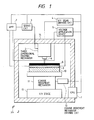
- Fig. 1 shows a schematic diagram of a recording and reproducing apparatus and a recording medium in a first embodiment of the present invention.
- numeral 1 denotes a microcomputer which controls an overall apparatus
- numeral 2 denotes a three-dimension drive mechanism which includes a cantilever to be described later
- numeral 3 denotes a servo circuit
- numeral 4 denotes an X-Y scan drive circuit
- numeral 5 denotes a voltage application device which applies a voltage across a probe and a recording medium
- numeral 6 denotes a probe electrode which is three-dimensionally displaceable by the three-dimension drive mechanism 2
- numeral 7 denotes a current amplifier
- numeral 8 denotes a recording medium layer
- numeral 9 denotes an underlying electrode
- numeral 10 denotes a substrate
- numeral 11 denotes a coarse displacement mechanism which includes a pulse motor and a lever mechanism to drive the recording medium in a Z direction
- numeral 12 denotes a coarse
- the probe 6 is brought to a predetermined distance from the recording medium 8 by the coarse displacement mechanism 11, and a rectangular pulse voltage having an amplitude of 3 volts and an width of 50 ns is applied as a write voltage by the voltage application device 5 so that an electrical conductivity of the recording medium 8 is changed to create an area having a different electrical resistance. In this manner, information is written.
- the probe 6 is scanned in the X and Y directions by the X-Y stage 13 and the three-dimension drive mechanism 2 and the write voltage is applied in accordance with the information to be written so that information is recorded two-dimensionally on the recording medium.
- a DC voltage (bias voltage) having an amplitude of 200 mV which is lower than the write voltage is applied as a read voltage to the recording medium 8 by the probe 6.
- the three-dimension drive mechanism 2 is feedback-controlled in the spacing direction (Z direction) such that a tunneling current detected by the current amplifier 7 and the servo circuit 3 under this condition is kept constant (0.1 nA), and the probe 6 is two-dimensionally scanned in the X and Y directions on the recording medium surface as it is done in the record mode.
- the amount of feedback in the Z direction varies in accordance with the recorded information (electrical conductivities) on the recording medium. Namely, the level of the probe goes up and down in accordance with the recording information value.
- the information can be reproduced by detecting the feedback signal or the Z position of the probe with respect to the record position (X-Y position).
- the control is effected by the microcomputer 1.
- the information may be reproduced by scanning the probe in the X and Y directions while keeping it constant in the Z direction and detecting the tunneling current created in accordance with the conductivity of the recording medium.
- the underlying electrode 9 is formed on a quartz glass substrate by depositing Cr to a thickness of 50 ⁇ by a vacuum vapor deposition method and depositing Au to a thickness of 300 ⁇ thereon by the same method.
- SOAZ silicon-bis-6-octylazlen
- the present invention is not limited to the above specific recording medium but various other recording media such as one disclosed in EP0272935A2 may be used.
- each set separately has the servo circuit 3, the X-Y scan drive circuit 4, the voltage application device 5 and the current amplifier 7, and the microcomputer 1 controls those units of the respective sets independently.
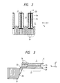
- Fig. 2 shows a detail of the three-dimension drive mechanism 2 and the probe 6 shown in Fig. 1, and Fig. 3 shows a sectional view thereof.
- the three-dimension drive mechanism 2 comprises a cantilever 22, a bimolf piezoelectric film 23 which serves as the displacement means, and a drive electrode 24 therefor.
- a piezo resistive element or a piezoelectric film which functions as a strain gauge is formed to serve as displacement detection means 25.
- the probe electrode and the three-dimension drive mechanism may be manufactured by micromechanics such as an Si anisotropy etching method taught by Calvin F. Quate, 4th International Conference on Scanning Tunneling Microscopy/Spectroscopy, '89, S10-2, and the displacement detection means 25 is patterned on an anisotropy etching mask layer 27.
- An insulation layer 28 is provided to insulate the displacement detection means 25 from the drive electrode 24.
- Fig. 4 shows a specific pattern of the displacement detection means 25. It shows X displacement detection means.
- the piezo resistive element which functions as the strain gauge is used as the displacement detection means 25.
- a stress generated in the piezo resistive element when the cantilever 22 is displaced is detected as a change in the resistance of the piezo resistive element. It is read by a read circuit 25A under the control of the microcomputer 1.
- the piezo resistive element may be manufactured by forming a polycrystalline silicon layer having a thickness of several ⁇ by a reduced pressure CVD device and ion-implanting boron to attain a resistivity of several m ⁇ cm.
- the piezoelectric film is used as the displacement detection means 25, a stress generated by the displacement of the cantilever 22 is detected as a charge generated in the piezoelectric film from the electrode 29.
- the piezoelectric film may be manufactured by forming an AlN film in a nitrogen or argon atmosphere by a magnetron sputtering method.
- Each of the cantilevers 22 shown in Fig. 2 is independently displaceable in X, Y and Z directions as shown in Fig. 5.
- two displacement detection means 25Y are arranged widthwise (Y direction) of the cantilever 22 as shown in Fig. 6, and stresses at the respective positions are detected from the outputs of the respective detection means 25Y by the microcomputer 1 through read circuits (not shown) as does the detection means 25, and a difference between the stresses is calculated to detect the Y displacement.
- two displacement detection means 25Z are arranged in the Z direction as shown in Fig. 7, and the Z displacement is detected from a difference between the detected stresses in the same manner as that for the Y direction.
- the detection means 25Y and 25Z may be formed on the same plane as the detection means 25 or they may be laminated in layers with an interposed insulation layer.
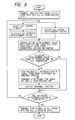
- the microcomputer 1 controls in the following manner.
- the information reproducing mode is first explained.
- a start command signal is sent from the microcomputer 1 to the respective three-dimension drive mechanism servo circuits 3.
- the command signal is also sent to the respective X-Y scan drive circuits 4.
- a control voltage is applied from the servo circuit 3 to the bimolf piezoelectric film 24 of the cantilever 22 to keep a current flowing between the probe 6 and the recording medium 8 at a constant level.
- a control voltage is also applied by the X-Y scan drive circuit 4 to the piezoelectric film 24 in order to drive the probe electrode 6 in the X and Y directions. In this manner, the information is reproduced based on the spacing between the probe 6 and the recording medium 8.
- the control voltages are also sent to the microcomputer 1.
- the displacement detection means on the cantilevers 22 also send the displacement information to the microcomputer 1.
- the microcomputer 1 calculates anticipated X, Y and Z displacements of the cantilever 22 for each three-dimension drive mechanism based on the control voltages sent thereto to produce anticipated values. It compares effective values of the actual displacements detected by the displacement detection means of the cantilever with the anticipated values, and if a difference is beyond a predetermined range, it determines an error in the operation of the three-dimension drive mechanism.
- the microcomputer 1 identifies the malfunctioned three-dimension drive mechanism by a display (not shown) or by voice for warning. In the reproducing mode, the signal from the probe electrode of the malfunctioned three-dimension drive mechanism is not reproduced.
- the servo circuit and the X-Y scan drive circuit for the malfunctioned three-dimension drive mechanism are deactivated.
- the servo circuit 3 is first activated and it is deactivated when the tunneling current reaches a predetermined level and the probe electrode 6 is fixed so as not to displace in the Z direction. This is done by a command signal from the microcomputer 1. Under this condition, the probe electrode 6 is scanned in the X and Y directions as it is done in the reproducing mode. An anticipated value of the displacement calculated based on the control voltage is compared with an effective value of an actual displacement detected by the displacement detection means to detect an error of each three-dimension drive mechanism. The detection operation is same as that in the reproduction mode except that the displacement calculated based on the Z direction control voltage after the deactivation of the servo circuit 3 is constant.
- the microcomputer 1 identifies the malfunctioned three-dimension drive mechanism by the display (not shown) or by voice output for warning. The recording voltage is not applied to the associated probe electrode, and the associated servo circuit and X-Y scan drive circuit are deactivated.
- an error may be detected when the three-dimension drive mechanism malfunctions as well as when the Z direction position control by the servo circuit 3 is disabled by an accident such as break of the probe electrode.
- the malfunction of the three-dimension drive mechanism as well as the trouble in the probe electrode can be detected.
- Fig. 9 shows a partial construction to illustrate a vicinity of the probe electrode 6 in the second embodiment.
- a plurality of probes are used, but since they are identical in construction, only one of them is shown.
- the probe electrode 6 and the three-dimension drive mechanism 2 are identical to those of the first embodiment.
- Numeral 31 denotes a tunneling current detection circuit which includes the current amplifier 7 of the first embodiment and a current-voltage conversion circuit which converts a current signal to a voltage signal
- numeral 32 a probe electrode control circuit which includes the servo circuit 3 for controlling the Z direction position of the probe electrode 6 based on an output of the detection circuit 31 and the X-Y scan drive circuit for controlling the X-Y scan of the probe electrode 6,
- numeral 33 denotes a correction circuit.
- Signal lines extending laterally from the circuits 31, 32 and 33 are connected to the microcomputer 1.
- the cantilever 22 and the circuits 31, 32 and 33 are formed integrally on the substrate to form a probe chip system 30. The other construction is identical to that of the first embodiment.
- the correction circuit 33 receives the control voltage applied from the control circuit 32 to the bimolf piezoelectric film of the cantilever 22 and the outputs of the displacement detection means, and compares the anticipated values of the displacements with the effective values of the actual displacements. In this manner, an error in the three-dimension drive mechanisms is detected. For the malfunctioned three-dimension drive mechanism detected by the comparison, a feedback command signal is issued to the control circuit 32 so that the cantilever 22 is further displaced by a difference between the effective value and the anticipated value. This is repeated until the effective value and the anticipated value match to attain the feedback correction. By such a feedback system, any error can be automatically corrected.
- the strain gauge shown in Figs. 4, 6 and 7 may be formed in a bridge circuit and the compensation circuit may be assembled into the correction circuit 33 ("High Technology Sensor" by Yamaka, Kyoritsu Publisher, p.116).
- the corresponding three-dimension drive mechanism may be disabled for correction by the microcomputer 1 to disactivate the control circuit 32 so as to stop the recording or the reproduction of the information by the corresponding probe electrode 6, and the correction-disabled three-dimension drive mechanism may be identified by the display (not shown).
- a self-alignment apparatus can be provided.
- the polycrystalline piezo resistive element is used as the strain gauge.
- the piezo resistive element may be formed in the substrate having the semiconductor by thermal diffusion, or a metal may be used as the strain gauge.
- the piezoelectric film may be made of a material having a piezoelectric effect such as AlN, TiBaO, PbZrTiO or PbTiO.
- the effect by the present invention is observed not only in the bimolf driven element but also it is effective in a static electric capacitance driven tunneling current generating probe by Wolfgung Deerel Paul (Japanese Patent Application 62-281138) and a thermal expansion driven cantilever (M. Elwenspoek, Proceedings of IEEE Micro-Electro-Mechanical Systems, 1989, Feb., P126).
- a plurality of sets of the probe electrodes and the three-dimension drive mechanisms are used although only one set may be used to detect the error.
- the present invention is not limited to the recording and reproducing apparatus but it is applicable to any apparatus which records and reproduces information by a probe such as an observation apparatus or a displacement measurement apparatus (encoder).
Abstract
Description
- The present invention relates to an apparatus for observing a surface of a material, finely machining the material and recording and reproducing information by a technique of a scanning tunneling microscope (STM) or the like.
- The observation, evaluation and fine machining of a semiconductor or high molecule material in the order of atom or molecule by using the STM technique (E. E. Ehrichs, 4th International Conference on Scanning Tunneling Microscopy/spectroscopy, '89, S13-3) and applications thereof to various fields such as a recorder have been being studied.
- Among others, a demand for a large capacity recorder for computer calculation information and image information is increasing more and more, and size reduction of the recorder is desired because of the fact that a size of a microprocessor has been reduced and a computing ability of the microprocessor has been improved. In order to meet the above requirements, a recording and reproducing apparatus have been proposed which records information on a recording area of 10 nm² at minimum by applying a voltage from a transducer having a tunneling current generating probe mounted on drive means to finely adjust a spacing to a recording medium in order to change a work function of a recording medium surface, and reads the information by detecting a change in a tunneling current due to the change in the work function.
- The above transducer is very effective means for not only the recorder but also material evaluation and fine machining of nanometer order.
- In the above apparatus, it is necessary to adjust a spacing between a probe and a medium so that processing is always performed at a proper spacing. For example, in the recording and reproducing apparatus described above, if the drive means malfunctions to separate the probe from the medium more than required, the information cannot be written onto the recording medium. If a similar malfunction occurs in the information record mode, the information is not correctly read and all signals read from the recording medium may be "0". Such malfunction may occur not only in the spacing adjustment but also when the probe is scanned parallelly to the medium surface. In the past, when such malfuction occurs, the written information is read by another apparatus for analysis or the read information is checked if it is not normal for a predetermined time period in order to detect the malfunction. Accordingly, a long time is taken to detect the error and it is time consuming.
- In the light of the above, it is an object of the present invention to provide an information recording and reproducing apparatus which can quickly detect an error (such as an error due to inproper spacing adjustment) to take counter measurement.
-
- Fig. 1 shows a schematic diagram of a recording and reproducing apparatus in accordance with one embodiment of the present invention,
- Fig. 2 shows a periphery of a tunneling current generating probe electrode of the apparatus,
- Fig. 3 shows a sectional view thereof,
- Fig. 4 shows a pattern of displacement detection means,
- Fig. 5 shows a displacement operation of a three-dimension drive mechanism,
- Fig. 6 shows a pattern of Y displacement detection means,
- Fig. 7 shows a pattern of Z displacement detection means,
- Fig. 8 shows a flow chart of the apparatus, and
- Fig. 9 shows a probe chip system in accordance with a second embodiment of the present invention.
- The embodiments of the present invention are now explained with reference to the drawings.
- Fig. 1 shows a schematic diagram of a recording and reproducing apparatus and a recording medium in a first embodiment of the present invention. In Fig. 1, numeral 1 denotes a microcomputer which controls an overall apparatus,
numeral 2 denotes a three-dimension drive mechanism which includes a cantilever to be described later,numeral 3 denotes a servo circuit, numeral 4 denotes an X-Y scan drive circuit,numeral 5 denotes a voltage application device which applies a voltage across a probe and a recording medium,numeral 6 denotes a probe electrode which is three-dimensionally displaceable by the three-dimension drive mechanism 2,numeral 7 denotes a current amplifier, numeral 8 denotes a recording medium layer,numeral 9 denotes an underlying electrode,numeral 10 denotes a substrate,numeral 11 denotes a coarse displacement mechanism which includes a pulse motor and a lever mechanism to drive the recording medium in a Z direction,numeral 12 denotes a coarse displacement mechanism drive circuit,numeral 13 denotes an X-Y stage for driving the recording medium in X and Y directions, andnumeral 14 denotes a closed frame which forms a closed structure. Theprobe 6 is brought to a predetermined distance from the recording medium 8 by thecoarse displacement mechanism 11, and a rectangular pulse voltage having an amplitude of 3 volts and an width of 50 ns is applied as a write voltage by thevoltage application device 5 so that an electrical conductivity of the recording medium 8 is changed to create an area having a different electrical resistance. In this manner, information is written. Theprobe 6 is scanned in the X and Y directions by theX-Y stage 13 and the three-dimension drive mechanism 2 and the write voltage is applied in accordance with the information to be written so that information is recorded two-dimensionally on the recording medium. On the other hand, in the reproducing mode, a DC voltage (bias voltage) having an amplitude of 200 mV which is lower than the write voltage is applied as a read voltage to the recording medium 8 by theprobe 6. The three-dimension drive mechanism 2 is feedback-controlled in the spacing direction (Z direction) such that a tunneling current detected by thecurrent amplifier 7 and theservo circuit 3 under this condition is kept constant (0.1 nA), and theprobe 6 is two-dimensionally scanned in the X and Y directions on the recording medium surface as it is done in the record mode. The amount of feedback in the Z direction varies in accordance with the recorded information (electrical conductivities) on the recording medium. Namely, the level of the probe goes up and down in accordance with the recording information value. The information can be reproduced by detecting the feedback signal or the Z position of the probe with respect to the record position (X-Y position). The control is effected by the microcomputer 1. - Alternatively, the information may be reproduced by scanning the probe in the X and Y directions while keeping it constant in the Z direction and detecting the tunneling current created in accordance with the conductivity of the recording medium.
- In the present embodiment, the
underlying electrode 9 is formed on a quartz glass substrate by depositing Cr to a thickness of 50 Å by a vacuum vapor deposition method and depositing Au to a thickness of 300 Å thereon by the same method. Four layers of SOAZ (squarilium-bis-6-octylazlen) are laminated thereon by an LB method to form the recording medium 8. The present invention is not limited to the above specific recording medium but various other recording media such as one disclosed in EP0272935A2 may be used. - In the present embodiment, only one set of the
probe electrode 6 and the three-dimension drive mechanism 2 is shown, although a plurality of sets are actually arranged to face the recording medium 8 so that information is recorded and reproduced simultaneously at a plurality of areas or the recording medium 8. Each set separately has theservo circuit 3, the X-Y scan drive circuit 4, thevoltage application device 5 and thecurrent amplifier 7, and the microcomputer 1 controls those units of the respective sets independently. - Fig. 2 shows a detail of the three-
dimension drive mechanism 2 and theprobe 6 shown in Fig. 1, and Fig. 3 shows a sectional view thereof. - The three-
dimension drive mechanism 2 comprises acantilever 22, a bimolfpiezoelectric film 23 which serves as the displacement means, and adrive electrode 24 therefor. A piezo resistive element or a piezoelectric film which functions as a strain gauge is formed to serve as displacement detection means 25. The probe electrode and the three-dimension drive mechanism may be manufactured by micromechanics such as an Si anisotropy etching method taught by Calvin F. Quate, 4th International Conference on Scanning Tunneling Microscopy/Spectroscopy, '89, S10-2, and the displacement detection means 25 is patterned on an anisotropyetching mask layer 27. Aninsulation layer 28 is provided to insulate the displacement detection means 25 from thedrive electrode 24. - Fig. 4 shows a specific pattern of the displacement detection means 25. It shows X displacement detection means.
- In the present embodiment, the piezo resistive element which functions as the strain gauge is used as the displacement detection means 25. A stress generated in the piezo resistive element when the
cantilever 22 is displaced is detected as a change in the resistance of the piezo resistive element. It is read by aread circuit 25A under the control of the microcomputer 1. The piezo resistive element may be manufactured by forming a polycrystalline silicon layer having a thickness of several Å by a reduced pressure CVD device and ion-implanting boron to attain a resistivity of several mΩ·cm. - Where the piezoelectric film is used as the displacement detection means 25, a stress generated by the displacement of the
cantilever 22 is detected as a charge generated in the piezoelectric film from theelectrode 29. The piezoelectric film may be manufactured by forming an AℓN film in a nitrogen or argon atmosphere by a magnetron sputtering method. - Each of the
cantilevers 22 shown in Fig. 2 is independently displaceable in X, Y and Z directions as shown in Fig. 5. For the Y displacement, two displacement detection means 25Y are arranged widthwise (Y direction) of thecantilever 22 as shown in Fig. 6, and stresses at the respective positions are detected from the outputs of the respective detection means 25Y by the microcomputer 1 through read circuits (not shown) as does the detection means 25, and a difference between the stresses is calculated to detect the Y displacement. For the Z displacement, two displacement detection means 25Z are arranged in the Z direction as shown in Fig. 7, and the Z displacement is detected from a difference between the detected stresses in the same manner as that for the Y direction. The detection means 25Y and 25Z may be formed on the same plane as the detection means 25 or they may be laminated in layers with an interposed insulation layer. By combining the displacement detection means of Figs. 4, 6 and 7, it is possible to detect the displacement of the probe in any of X, Y and Z directions. - In the present embodiment, the microcomputer 1 controls in the following manner. The information reproducing mode is first explained.
- A start command signal is sent from the microcomputer 1 to the respective three-dimension drive
mechanism servo circuits 3. The command signal is also sent to the respective X-Y scan drive circuits 4. A control voltage is applied from theservo circuit 3 to the bimolfpiezoelectric film 24 of thecantilever 22 to keep a current flowing between theprobe 6 and the recording medium 8 at a constant level. A control voltage is also applied by the X-Y scan drive circuit 4 to thepiezoelectric film 24 in order to drive theprobe electrode 6 in the X and Y directions. In this manner, the information is reproduced based on the spacing between theprobe 6 and the recording medium 8. The control voltages are also sent to the microcomputer 1. The displacement detection means on thecantilevers 22 also send the displacement information to the microcomputer 1. The microcomputer 1 calculates anticipated X, Y and Z displacements of thecantilever 22 for each three-dimension drive mechanism based on the control voltages sent thereto to produce anticipated values. It compares effective values of the actual displacements detected by the displacement detection means of the cantilever with the anticipated values, and if a difference is beyond a predetermined range, it determines an error in the operation of the three-dimension drive mechanism. The microcomputer 1 identifies the malfunctioned three-dimension drive mechanism by a display (not shown) or by voice for warning. In the reproducing mode, the signal from the probe electrode of the malfunctioned three-dimension drive mechanism is not reproduced. The servo circuit and the X-Y scan drive circuit for the malfunctioned three-dimension drive mechanism are deactivated. - The control by the microcomputer 1 in the information record mode is now explained.
- The
servo circuit 3 is first activated and it is deactivated when the tunneling current reaches a predetermined level and theprobe electrode 6 is fixed so as not to displace in the Z direction. This is done by a command signal from the microcomputer 1. Under this condition, theprobe electrode 6 is scanned in the X and Y directions as it is done in the reproducing mode. An anticipated value of the displacement calculated based on the control voltage is compared with an effective value of an actual displacement detected by the displacement detection means to detect an error of each three-dimension drive mechanism. The detection operation is same as that in the reproduction mode except that the displacement calculated based on the Z direction control voltage after the deactivation of theservo circuit 3 is constant. The microcomputer 1 identifies the malfunctioned three-dimension drive mechanism by the display (not shown) or by voice output for warning. The recording voltage is not applied to the associated probe electrode, and the associated servo circuit and X-Y scan drive circuit are deactivated. - The above control is shown in a flow chart of Fig. 8.
- In the apparatus of the present embodiment, an error may be detected when the three-dimension drive mechanism malfunctions as well as when the Z direction position control by the
servo circuit 3 is disabled by an accident such as break of the probe electrode. Thus, the malfunction of the three-dimension drive mechanism as well as the trouble in the probe electrode can be detected. - A second embodiment of the present invention is now explained.
- Fig. 9 shows a partial construction to illustrate a vicinity of the
probe electrode 6 in the second embodiment. In the present embodiment, a plurality of probes are used, but since they are identical in construction, only one of them is shown. Theprobe electrode 6 and the three-dimension drive mechanism 2 are identical to those of the first embodiment.Numeral 31 denotes a tunneling current detection circuit which includes thecurrent amplifier 7 of the first embodiment and a current-voltage conversion circuit which converts a current signal to a voltage signal, numeral 32 a probe electrode control circuit which includes theservo circuit 3 for controlling the Z direction position of theprobe electrode 6 based on an output of thedetection circuit 31 and the X-Y scan drive circuit for controlling the X-Y scan of theprobe electrode 6, and numeral 33 denotes a correction circuit. Signal lines extending laterally from thecircuits cantilever 22 and thecircuits probe chip system 30. The other construction is identical to that of the first embodiment. - In the present embodiment, the
correction circuit 33 receives the control voltage applied from thecontrol circuit 32 to the bimolf piezoelectric film of thecantilever 22 and the outputs of the displacement detection means, and compares the anticipated values of the displacements with the effective values of the actual displacements. In this manner, an error in the three-dimension drive mechanisms is detected. For the malfunctioned three-dimension drive mechanism detected by the comparison, a feedback command signal is issued to thecontrol circuit 32 so that thecantilever 22 is further displaced by a difference between the effective value and the anticipated value. This is repeated until the effective value and the anticipated value match to attain the feedback correction. By such a feedback system, any error can be automatically corrected. - For the purpose of temperature compensation of the displacement detection means, the strain gauge shown in Figs. 4, 6 and 7 may be formed in a bridge circuit and the compensation circuit may be assembled into the correction circuit 33 ("High Technology Sensor" by Yamaka, Kyoritsu Publisher, p.116). If there is no change in the output of the displacement detection means when a command signal is issued from the
correction circuit 33 or if the control voltage to be applied by thecontrol circuit 32 in response to the command signal is abnormal value (for example, beyond a permissible range of the bimolf piezoelectric film), the corresponding three-dimension drive mechanism may be disabled for correction by the microcomputer 1 to disactivate thecontrol circuit 32 so as to stop the recording or the reproduction of the information by thecorresponding probe electrode 6, and the correction-disabled three-dimension drive mechanism may be identified by the display (not shown). - Where such a system is formed on a substrate having a semiconductor, a self-alignment apparatus can be provided.
- In the above embodiments, the polycrystalline piezo resistive element is used as the strain gauge. Alternatively, the piezo resistive element may be formed in the substrate having the semiconductor by thermal diffusion, or a metal may be used as the strain gauge. The piezoelectric film may be made of a material having a piezoelectric effect such as AℓN, TiBaO, PbZrTiO or PbTiO. The effect by the present invention is observed not only in the bimolf driven element but also it is effective in a static electric capacitance driven tunneling current generating probe by Wolfgung Deerel Paul (Japanese Patent Application 62-281138) and a thermal expansion driven cantilever (M. Elwenspoek, Proceedings of IEEE Micro-Electro-Mechanical Systems, 1989, Feb., P126).
- In the above embodiments, a plurality of sets of the probe electrodes and the three-dimension drive mechanisms are used although only one set may be used to detect the error.
- The present invention is not limited to the recording and reproducing apparatus but it is applicable to any apparatus which records and reproduces information by a probe such as an observation apparatus or a displacement measurement apparatus (encoder).
Claims (28)
- An apparatus for recording and/or reproducing information to and/or from a recording medium comprising:
a probe arranged to face said recording medium for recording and/or reproducing information;
adjusting means for adjusting a relative positional relationship between said recording medium and said probe;
error detection means for detecting an error in said probe side during the adjustment of the relative positional relationship; and
means for recording and/or reproducing information to and/or from said recording medium by said probe. - An apparatus according to Claim 1, wherein said adjusting means includes displacement means for displacing said probe, and said error detection means includes displacement detection means for detecting a displacement status of said probe.
- An apparatus according to Claim 2, wherein said error detection means compares a control signal to said displacement means and an output of said displacement detection means to detect the error.
- An apparatus accordig to Claim 2, wherein said displacement means includes a cantilever which supports said probe at a free end thereof and a displacement element for deforming said cantilever.
- An apparatus according to Claim 4, wherein said displacement detection means includes strain detection means for detecting a strain generated in said cantilever.
- An apparatus according to Claim 5, wherein said strain detection means includes a strain gauge or a piezoelectric element mounted on said cantilever.
- An apparatus according to Claim 1, wherein said means for recording and/or reproducing information includes voltage application means for applying a voltage to write or read information across said probe and said recording medium.
- An apparatus according to Claim 7, wherein said voltage application means applies a write voltage to record information to said recording medium.
- An apparatus according to Claim 7 further comprising current detection means for detecting a current flowing between said probe and said recording medium when a read voltage is applied by said voltage application means.
- An apparatus according to Claim 9, wherein said current is a tunneling current.
- An apparatus according to Claim 1 further comprising means for stopping a recording or reproduction of information in accordance with an output of said error detection means.
- An apparatus according to Claim 1 further comprising means for correcting the relative positional relationship in accordance with an output of said error detection means.
- An apparatus according to Claim 1, wherein a plurality of said probes are provided, and said adjusting means and said error detection means are provided for each of said probes.
- An apparatus for recording and/or reproducing information to and/or from a recording medium comprising:
a probe arranged to face said recording medium for recording and/or reproducing information;
displacement means for displacing said probe;
displacement detection means for detecting an operating status of said displacement means;
means for feeding back to said displacement means to make an output of said displacement detection means to assume a predetermined value; and
means for recording and/or reproducing information to and/or from said recording medium by said probe. - An apparatus according to Claim 14, wherein said displacement means displaces said probe three-dimensionally.
- An apparatus according to Claim 14, wherein said displacement means includes a cantilever which supports said probe at a free end thereof and a displacement element for deforming said cantilever.
- An apparatus according to Claim 16, wherein said displacement detection means includes strain detection means for detecting a strain generated in said cantilever.
- An apparatus according to Claim 17, wherein said strain detection means includes a strain gauge or a piezoelectric element mounted on said cantilever.
- An apparatus according to Claim 14, wherein a plurality of said probes are provided, and said displacement means and said displacement detection means are provided for each of said probes.
- An apparatus according to Claim 14, wherein said means for recording and/or reproducing information includes voltage application means for applying a voltage to write or read information across said probe and said recording medium.
- An apparatus for inputting and/or outputting information comprising:
a probe;
displacement means for displacing said probe; and
displacement detection means for detecting an operating status of said displacement means. - An apparatus according to Claim 21, wherein said displacement means displaces said probe three-dimensionally.
- An apparatus according to Claim 22, wherein said displacement means includes a cantilever which supports said probe at a free end thereof and a displacement element for deforming said cantilever.
- An apparatus according to Claim 23, wherein said displacement detection means includes strain detection means for detecting a strain generated in said cantilever.
- An apparatus according to Claim 24, wherein said strain detection means includes a strain gauge or a piezoelectric element mounted on said cantilever.
- An apparatus according to Claim 21, wherein a plurality of said probes are provided, and said displacement means and said displacement detection means are provided for each of said probes.
- An apparatus for inputting and/or outputting information to and/or from an information carrier comprising:
a probe arranged to face said information carrier for recording and/or reproducing information;
adjusting means for adjusting a relative positional relationship between said information carrier and said probe;
error detection means for detecting an error in said probe side during the adjustment of the relative positional relationship; and
means for inputting and/or outputting information to and/or from said information carrier by said probe. - An apparatus for inputting and/or outputting information to and/or from an information carrier comprising:
a probe arranged to face said information carrier for recording and/or reproducing information;
displacement means for displacing said probe;
displacement detection means for detecting an operating status of said displacement means;
means for feeding back to said displacement means to make an output of said displacement detection means to assume a predetermined value; and
means for inputting and/or outputting information to and/or from said information carrier by said probe.
Applications Claiming Priority (2)
| Application Number | Priority Date | Filing Date | Title |
|---|---|---|---|
| JP104061/90 | 1990-04-18 | ||
| JP2104061A JPH041949A (en) | 1990-04-18 | 1990-04-18 | Information input and/or output device |
Publications (2)
| Publication Number | Publication Date |
|---|---|
| EP0452851A1 true EP0452851A1 (en) | 1991-10-23 |
| EP0452851B1 EP0452851B1 (en) | 1997-07-09 |
Family
ID=14370667
Family Applications (1)
| Application Number | Title | Priority Date | Filing Date |
|---|---|---|---|
| EP91105973A Expired - Lifetime EP0452851B1 (en) | 1990-04-18 | 1991-04-15 | Information recording/reproducing apparatus |
Country Status (5)
| Country | Link |
|---|---|
| US (1) | US5313451A (en) |
| EP (1) | EP0452851B1 (en) |
| JP (1) | JPH041949A (en) |
| CA (1) | CA2040701C (en) |
| DE (1) | DE69126736T2 (en) |
Cited By (1)
| Publication number | Priority date | Publication date | Assignee | Title |
|---|---|---|---|---|
| EP1486955A2 (en) * | 2003-06-13 | 2004-12-15 | Alps Electric Co., Ltd. | High precision positioning apparatus for optical recording medium |
Families Citing this family (15)
| Publication number | Priority date | Publication date | Assignee | Title |
|---|---|---|---|---|
| JPH0696714A (en) * | 1992-09-14 | 1994-04-08 | Hitachi Ltd | Surface working device and recording device |
| US5418771A (en) * | 1993-02-25 | 1995-05-23 | Canon Kabushiki Kaisha | Information processing apparatus provided with surface aligning mechanism between probe head substrate and recording medium substrate |
| JP3576655B2 (en) * | 1995-09-14 | 2004-10-13 | キヤノン株式会社 | Method for manufacturing micro probe, female substrate for manufacturing the same, and method for manufacturing probe having micro probe |
| US5874668A (en) * | 1995-10-24 | 1999-02-23 | Arch Development Corporation | Atomic force microscope for biological specimens |
| US6066265A (en) * | 1996-06-19 | 2000-05-23 | Kionix, Inc. | Micromachined silicon probe for scanning probe microscopy |
| US5889541A (en) * | 1996-10-09 | 1999-03-30 | Xerox Corporation | Two-dimensional print cell array apparatus and method for delivery of toner for printing images |
| JPH10282130A (en) * | 1997-04-01 | 1998-10-23 | Canon Inc | Probe and scanning probe microscope using it |
| DE19902413C1 (en) * | 1999-01-22 | 2000-05-31 | Daimler Chrysler Ag | Calibration method for piezoelectric control drive involves automatically detecting control parameters and associated control positions by detecting stop times from capacitance changes |
| KR100331451B1 (en) * | 2000-05-10 | 2002-04-09 | 윤종용 | Rewritable data storage using carbonaceous material and writing and reading method thereof |
| KR100474844B1 (en) * | 2001-12-08 | 2005-03-08 | 삼성전자주식회사 | Lorentz force microscope and method of measuring magnetic domain utilizing lorentz force |
| KR100453973B1 (en) * | 2002-04-23 | 2004-10-20 | 전자부품연구원 | Fine optical switch using micro piezoelectric actuator |
| KR100745756B1 (en) * | 2006-01-04 | 2007-08-02 | 삼성전자주식회사 | Micro actuator and data storage apparatus employing the same |
| DE102006008584A1 (en) * | 2006-02-24 | 2007-09-06 | Atmel Germany Gmbh | Manufacturing process for integrated piezo components |
| US8104093B2 (en) | 2008-03-28 | 2012-01-24 | Empire Technology Development Llc | Magnetic sensor and scanning microscope |
| JP6544037B2 (en) * | 2015-05-18 | 2019-07-17 | 株式会社リコー | Power generation element unit and power generation apparatus |
Citations (3)
| Publication number | Priority date | Publication date | Assignee | Title |
|---|---|---|---|---|
| EP0247219A1 (en) * | 1986-05-27 | 1987-12-02 | International Business Machines Corporation | Direct access storage unit |
| US4841191A (en) * | 1987-02-20 | 1989-06-20 | Hitachi, Ltd. | Piezoelectric actuator control apparatus |
| EP0360975A2 (en) * | 1988-09-30 | 1990-04-04 | Rockwell International Corporation | Piezoelectric actuator |
Family Cites Families (21)
| Publication number | Priority date | Publication date | Assignee | Title |
|---|---|---|---|---|
| US3632900A (en) * | 1969-12-31 | 1972-01-04 | Ibm | Magnetic transducer displacement control system |
| JPS56115084A (en) * | 1980-02-16 | 1981-09-10 | Sony Corp | Video signal reproducer |
| JPH0695377B2 (en) * | 1985-03-12 | 1994-11-24 | ソニー株式会社 | Bimorph drive for bimorph heads |
| US4764818A (en) * | 1986-02-03 | 1988-08-16 | Electron Beam Memories | Electron beam memory system with improved high rate digital beam pulsing system |
| EP0272935B1 (en) * | 1986-12-24 | 1994-03-16 | Canon Kabushiki Kaisha | Recording device and reproducing device |
| EP0307211A3 (en) * | 1987-09-10 | 1991-05-15 | Seiko Instruments Inc. | Memory reading device |
| US4906840A (en) * | 1988-01-27 | 1990-03-06 | The Board Of Trustees Of Leland Stanford Jr., University | Integrated scanning tunneling microscope |
| JP2936545B2 (en) * | 1988-06-24 | 1999-08-23 | 株式会社日立製作所 | Scanning probe microscope |
| JPH0238904A (en) * | 1988-07-29 | 1990-02-08 | Hitachi Ltd | Fine displacing mechanism and scan type tunnel microscope using same |
| JP2547869B2 (en) * | 1988-11-09 | 1996-10-23 | キヤノン株式会社 | PROBE UNIT, METHOD FOR DRIVING THE PROBE, AND SCANNING TUNNEL CURRENT DETECTION DEVICE HAVING THE PROBE UNIT |
| JPH02206043A (en) * | 1989-02-03 | 1990-08-15 | Olympus Optical Co Ltd | Storage device |
| US5015850A (en) * | 1989-06-20 | 1991-05-14 | The Board Of Trustees Of The Leland Stanford Junior University | Microfabricated microscope assembly |
| US5142424A (en) * | 1989-07-12 | 1992-08-25 | Yotaro Hatamura | Floatable information-reading head support configured to prevent forward pitch |
| US4992659A (en) * | 1989-07-27 | 1991-02-12 | International Business Machines Corporation | Near-field lorentz force microscopy |
| JPH03184355A (en) * | 1989-12-13 | 1991-08-12 | Mitsubishi Electric Corp | Wafer prober |
| US5031463A (en) * | 1990-03-20 | 1991-07-16 | Sensortronics, Inc. | Load cell output correction circuitry |
| US5255259A (en) * | 1990-04-18 | 1993-10-19 | Canon Kabushiki Kaisha | Method of access to recording medium, and apparatus and method for processing information |
| US5115664A (en) * | 1990-06-25 | 1992-05-26 | Ibm Corporation | Tunable feedback transducer for transient friction measurement |
| JP2915554B2 (en) * | 1990-11-19 | 1999-07-05 | オリンパス光学工業株式会社 | Barrier height measurement device |
| JP3000492B2 (en) * | 1991-04-22 | 2000-01-17 | キヤノン株式会社 | Information processing device |
| US5161149A (en) * | 1991-07-22 | 1992-11-03 | The Johns Hopkins University | Electron density storage device and method using STM |
-
1990
- 1990-04-18 JP JP2104061A patent/JPH041949A/en active Pending
-
1991
- 1991-04-15 DE DE69126736T patent/DE69126736T2/en not_active Expired - Fee Related
- 1991-04-15 EP EP91105973A patent/EP0452851B1/en not_active Expired - Lifetime
- 1991-04-17 CA CA002040701A patent/CA2040701C/en not_active Expired - Fee Related
-
1992
- 1992-09-10 US US07/942,821 patent/US5313451A/en not_active Expired - Lifetime
Patent Citations (3)
| Publication number | Priority date | Publication date | Assignee | Title |
|---|---|---|---|---|
| EP0247219A1 (en) * | 1986-05-27 | 1987-12-02 | International Business Machines Corporation | Direct access storage unit |
| US4841191A (en) * | 1987-02-20 | 1989-06-20 | Hitachi, Ltd. | Piezoelectric actuator control apparatus |
| EP0360975A2 (en) * | 1988-09-30 | 1990-04-04 | Rockwell International Corporation | Piezoelectric actuator |
Non-Patent Citations (2)
| Title |
|---|
| PATENT ABSTRACTS OF JAPAN, vol. 14, no. 195 (P-1039) 20 April 1990; & JP-A-02 038 904 (HITACHI LTD) 08 February 1990 * |
| REVIEW OF SCIENTIFIC INSTRUMENTS, vol. 60, no. 9, September 1989, NEW YORK, US; pages 3024 - 3029; KAZUYOSHI SUGIHARA et Al.: "Piezoelectrically driven xy-teta table for submicron lithography systems" * |
Cited By (2)
| Publication number | Priority date | Publication date | Assignee | Title |
|---|---|---|---|---|
| EP1486955A2 (en) * | 2003-06-13 | 2004-12-15 | Alps Electric Co., Ltd. | High precision positioning apparatus for optical recording medium |
| EP1486955A3 (en) * | 2003-06-13 | 2007-08-29 | Alps Electric Co., Ltd. | High precision positioning apparatus for optical recording medium |
Also Published As
| Publication number | Publication date |
|---|---|
| CA2040701C (en) | 1999-01-26 |
| JPH041949A (en) | 1992-01-07 |
| CA2040701A1 (en) | 1991-10-19 |
| DE69126736D1 (en) | 1997-08-14 |
| US5313451A (en) | 1994-05-17 |
| EP0452851B1 (en) | 1997-07-09 |
| DE69126736T2 (en) | 1998-01-08 |
Similar Documents
| Publication | Publication Date | Title |
|---|---|---|
| US5412641A (en) | Information recording/reproducing apparatus for recording/reproducing information with probes | |
| EP0452851B1 (en) | Information recording/reproducing apparatus | |
| JP3246987B2 (en) | Information processing device with multi-probe control circuit | |
| US5506829A (en) | Cantilever probe and apparatus using the same | |
| EP0361932B1 (en) | Scanning tunnel-current-detecting device and method | |
| EP0516418B1 (en) | Probe-driving mechanism, production thereof, and apparatus and piezoelectric actuator employing the same | |
| US5220555A (en) | Scanning tunnel-current-detecting device and method for detecting tunnel current and scanning tunnelling microscope and recording/reproducing device using thereof | |
| JP3450349B2 (en) | Cantilever probe | |
| US5717680A (en) | Information processing apparatus with mechanism for adjusting interval between substrate for supporting a plurality of probes and recording medium | |
| US5371728A (en) | Information recording/reproducing apparatus using probe | |
| US5418771A (en) | Information processing apparatus provided with surface aligning mechanism between probe head substrate and recording medium substrate | |
| JPH10312592A (en) | Information processor and processing method | |
| US5371727A (en) | Scanning tunnel microscopy information processing system with noise detection to correct the tracking mechanism | |
| US5978326A (en) | Information processing apparatus using an offset signal to control the position of a probe | |
| JPH06241781A (en) | Cantilever, cantilever type probe using this, scanning tunneling microscope using cantilever type probe, information processing device | |
| JP3234722B2 (en) | Arc-shaped warped lever type actuator, method of driving the actuator, and information processing apparatus using information input / output probe | |
| JP3060142B2 (en) | Driving method of cantilever type displacement element, scanning tunneling microscope, information processing apparatus, and cantilever type displacement element | |
| JPH0875761A (en) | Scanning probe microscope as well as processing apparatus using the microscope and data-processing apparatus | |
| JP3234952B2 (en) | Probe unit, scanning tunneling microscope and information processing apparatus using the same | |
| JPH04359108A (en) | Inclination measuring mechanism | |
| JPH06119665A (en) | Information recording and reproducing device | |
| JPH04205739A (en) | Cantilever type probe and information processor using it | |
| JPH06241778A (en) | Surface observing method, record reproducing method, surface observing device and record reproducing device using these | |
| JPH05334737A (en) | Tracking method and information processor using the same | |
| JPH04155633A (en) | Information reading/inputting apparatus |
Legal Events
| Date | Code | Title | Description |
|---|---|---|---|
| PUAI | Public reference made under article 153(3) epc to a published international application that has entered the european phase |
Free format text: ORIGINAL CODE: 0009012 |
|
| AK | Designated contracting states |
Kind code of ref document: A1 Designated state(s): BE CH DE ES FR GB IT LI NL SE |
|
| 17P | Request for examination filed |
Effective date: 19920306 |
|
| 17Q | First examination report despatched |
Effective date: 19940727 |
|
| GRAG | Despatch of communication of intention to grant |
Free format text: ORIGINAL CODE: EPIDOS AGRA |
|
| GRAH | Despatch of communication of intention to grant a patent |
Free format text: ORIGINAL CODE: EPIDOS IGRA |
|
| GRAH | Despatch of communication of intention to grant a patent |
Free format text: ORIGINAL CODE: EPIDOS IGRA |
|
| GRAA | (expected) grant |
Free format text: ORIGINAL CODE: 0009210 |
|
| AK | Designated contracting states |
Kind code of ref document: B1 Designated state(s): BE CH DE ES FR GB IT LI NL SE |
|
| PG25 | Lapsed in a contracting state [announced via postgrant information from national office to epo] |
Ref country code: NL Free format text: LAPSE BECAUSE OF FAILURE TO SUBMIT A TRANSLATION OF THE DESCRIPTION OR TO PAY THE FEE WITHIN THE PRESCRIBED TIME-LIMIT Effective date: 19970709 Ref country code: LI Free format text: LAPSE BECAUSE OF FAILURE TO SUBMIT A TRANSLATION OF THE DESCRIPTION OR TO PAY THE FEE WITHIN THE PRESCRIBED TIME-LIMIT Effective date: 19970709 Ref country code: ES Free format text: THE PATENT HAS BEEN ANNULLED BY A DECISION OF A NATIONAL AUTHORITY Effective date: 19970709 Ref country code: CH Free format text: LAPSE BECAUSE OF FAILURE TO SUBMIT A TRANSLATION OF THE DESCRIPTION OR TO PAY THE FEE WITHIN THE PRESCRIBED TIME-LIMIT Effective date: 19970709 Ref country code: BE Effective date: 19970709 |
|
| REG | Reference to a national code |
Ref country code: CH Ref legal event code: EP |
|
| REF | Corresponds to: |
Ref document number: 69126736 Country of ref document: DE Date of ref document: 19970814 |
|
| ET | Fr: translation filed | ||
| ITF | It: translation for a ep patent filed |
Owner name: PROROGA CONCESSA IN DATA: 09.12.97;SOCIETA' ITALIA |
|
| PG25 | Lapsed in a contracting state [announced via postgrant information from national office to epo] |
Ref country code: SE Effective date: 19971009 |
|
| NLV1 | Nl: lapsed or annulled due to failure to fulfill the requirements of art. 29p and 29m of the patents act | ||
| REG | Reference to a national code |
Ref country code: CH Ref legal event code: PL |
|
| PLBE | No opposition filed within time limit |
Free format text: ORIGINAL CODE: 0009261 |
|
| STAA | Information on the status of an ep patent application or granted ep patent |
Free format text: STATUS: NO OPPOSITION FILED WITHIN TIME LIMIT |
|
| 26N | No opposition filed | ||
| REG | Reference to a national code |
Ref country code: GB Ref legal event code: IF02 |
|
| PGFP | Annual fee paid to national office [announced via postgrant information from national office to epo] |
Ref country code: DE Payment date: 20050407 Year of fee payment: 15 |
|
| PGFP | Annual fee paid to national office [announced via postgrant information from national office to epo] |
Ref country code: FR Payment date: 20050408 Year of fee payment: 15 |
|
| PGFP | Annual fee paid to national office [announced via postgrant information from national office to epo] |
Ref country code: GB Payment date: 20050413 Year of fee payment: 15 |
|
| PG25 | Lapsed in a contracting state [announced via postgrant information from national office to epo] |
Ref country code: GB Free format text: LAPSE BECAUSE OF NON-PAYMENT OF DUE FEES Effective date: 20060415 |
|
| PGFP | Annual fee paid to national office [announced via postgrant information from national office to epo] |
Ref country code: IT Payment date: 20060430 Year of fee payment: 16 |
|
| PG25 | Lapsed in a contracting state [announced via postgrant information from national office to epo] |
Ref country code: DE Free format text: LAPSE BECAUSE OF NON-PAYMENT OF DUE FEES Effective date: 20061101 |
|
| GBPC | Gb: european patent ceased through non-payment of renewal fee |
Effective date: 20060415 |
|
| REG | Reference to a national code |
Ref country code: FR Ref legal event code: ST Effective date: 20061230 |
|
| PG25 | Lapsed in a contracting state [announced via postgrant information from national office to epo] |
Ref country code: FR Free format text: LAPSE BECAUSE OF NON-PAYMENT OF DUE FEES Effective date: 20060502 |
|
| PG25 | Lapsed in a contracting state [announced via postgrant information from national office to epo] |
Ref country code: IT Free format text: LAPSE BECAUSE OF NON-PAYMENT OF DUE FEES Effective date: 20070415 |