EP0454891A1 - Light emitting diode array - Google Patents
Light emitting diode array Download PDFInfo
- Publication number
- EP0454891A1 EP0454891A1 EP90108461A EP90108461A EP0454891A1 EP 0454891 A1 EP0454891 A1 EP 0454891A1 EP 90108461 A EP90108461 A EP 90108461A EP 90108461 A EP90108461 A EP 90108461A EP 0454891 A1 EP0454891 A1 EP 0454891A1
- Authority
- EP
- European Patent Office
- Prior art keywords
- layer
- semiconductor
- insulating layer
- electrode
- light emitting
- Prior art date
- Legal status (The legal status is an assumption and is not a legal conclusion. Google has not performed a legal analysis and makes no representation as to the accuracy of the status listed.)
- Ceased
Links
Images


Classifications
-
- H—ELECTRICITY
- H01—ELECTRIC ELEMENTS
- H01L—SEMICONDUCTOR DEVICES NOT COVERED BY CLASS H10
- H01L33/00—Semiconductor devices with at least one potential-jump barrier or surface barrier specially adapted for light emission; Processes or apparatus specially adapted for the manufacture or treatment thereof or of parts thereof; Details thereof
- H01L33/36—Semiconductor devices with at least one potential-jump barrier or surface barrier specially adapted for light emission; Processes or apparatus specially adapted for the manufacture or treatment thereof or of parts thereof; Details thereof characterised by the electrodes
- H01L33/38—Semiconductor devices with at least one potential-jump barrier or surface barrier specially adapted for light emission; Processes or apparatus specially adapted for the manufacture or treatment thereof or of parts thereof; Details thereof characterised by the electrodes with a particular shape
- H01L33/385—Semiconductor devices with at least one potential-jump barrier or surface barrier specially adapted for light emission; Processes or apparatus specially adapted for the manufacture or treatment thereof or of parts thereof; Details thereof characterised by the electrodes with a particular shape the electrode extending at least partially onto a side surface of the semiconductor body
-
- B—PERFORMING OPERATIONS; TRANSPORTING
- B41—PRINTING; LINING MACHINES; TYPEWRITERS; STAMPS
- B41J—TYPEWRITERS; SELECTIVE PRINTING MECHANISMS, i.e. MECHANISMS PRINTING OTHERWISE THAN FROM A FORME; CORRECTION OF TYPOGRAPHICAL ERRORS
- B41J2/00—Typewriters or selective printing mechanisms characterised by the printing or marking process for which they are designed
- B41J2/435—Typewriters or selective printing mechanisms characterised by the printing or marking process for which they are designed characterised by selective application of radiation to a printing material or impression-transfer material
- B41J2/447—Typewriters or selective printing mechanisms characterised by the printing or marking process for which they are designed characterised by selective application of radiation to a printing material or impression-transfer material using arrays of radiation sources
- B41J2/45—Typewriters or selective printing mechanisms characterised by the printing or marking process for which they are designed characterised by selective application of radiation to a printing material or impression-transfer material using arrays of radiation sources using light-emitting diode [LED] or laser arrays
-
- H—ELECTRICITY
- H01—ELECTRIC ELEMENTS
- H01L—SEMICONDUCTOR DEVICES NOT COVERED BY CLASS H10
- H01L27/00—Devices consisting of a plurality of semiconductor or other solid-state components formed in or on a common substrate
- H01L27/15—Devices consisting of a plurality of semiconductor or other solid-state components formed in or on a common substrate including semiconductor components with at least one potential-jump barrier or surface barrier specially adapted for light emission
- H01L27/153—Devices consisting of a plurality of semiconductor or other solid-state components formed in or on a common substrate including semiconductor components with at least one potential-jump barrier or surface barrier specially adapted for light emission in a repetitive configuration, e.g. LED bars
Definitions
- the present invention relates to a light emitting diode (LED) array employable in an electronic printer for photography, and particularly to a structure of P and N electrodes on the LED array.
- LED light emitting diode
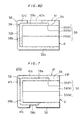
- Fig. 1 illustrates the structure of a conventional LED array 1.
- the LED array 1 comprises a semiconductor body 10 having an N-GaAs layer 3, an N-Al x Ga 1-x As layer 4 and P-Al x Ga 1-x As regions 5.
- An N-electrode layer 2 is formed on the bottom surface of the semiconductor body 10, while an insulating layer 8 is provided on the top surface of the semiconductor body 10.
- the insulating layer 8 has a linear array of rectangular windows 9, which are defined on the P-regions 5.
- P-electrode layers 11 are formed on the insulating layer 8 and respective end portions thereof are in contact with the top surfaces of the P-regions 5 through the windows 9.
- Fig. 2 is a schematic diagram showing the situation in which the LED array 1 is employed in an electronic printer for photography.
- the LED array 1 is fixed to a base plate 21 such as a printed board, and the electric connection between the LED array 1 and the base plate 21 is attained through die bonding and wire bonding.
- a self-focussing lens array (SLA) 22 is supported by a supporting member (not shown) so that the windows 9 (Fig. 1) face to the SLA 22 across a gap therebetween.
- a photosensitive drum 23 is rotatably provided and the center of the drum 23 is located on a line passing through the LED array 1 and the SLA 22.
- An image signal is transmitted to an LED drive circuit (not shown), and in response to the image signal, the LED drive circuit selectively supplies electric power to the LEDs included in the LED array 1 through the electrodes 2 and 11.
- the LEDs supplied with the electric power generate light L1 at the PN junctions thereof and emit the light L1 through the windows 9.
- the SLA 22 converts the light L1 into converging light L2, which is applied to a photosensitive surface 24 of the drum 23.
- the SLA 22 is effective for preventing the light spot from spreading on the photosensitive surface 24 of the drum 23.
- the photosensitive surface 24 of the drum 23 Prior to the exposure to the light L2, the photosensitive surface 24 of the drum 23 is electrostatically charged to a negative level.
- the photosensitive surface 24 When the light L2 is applied to the photosensitive surface 24, only the part of the surface 24 exposed to the light L2 is discharged. Therefore, a latent image is obtained on the photosensitive surface 24 by repeating the light generating process while rotating the drum 23 around the axis thereof. Then, the photosensitive surface 24 is supplied with toner charged to a negative level, and the toner stays only on the discharged part of the surface 24 since the toner cannot stay on the non-discharged part to an electrostatic repulsive force. The toner particles staying on the surface 24 are transferred onto paper, and then, the image thus obtained is fixed by heat and pressure.
- the transmission efficiency of light is only about several percent in the LED array head consisting of the LED array 1, the base plate 21, the SLA 22 and a driver (not shown). This is because the SLA 22, which has a relatively low transmission efficiency of light, should be provided in the LED array head in the conventional structure.
- the LED array 1 since the electrode layers 2 and 11 are located on opposite surfaces of the semiconductor body 10, the LED array 1 must be mounted on the base plate 21 through die bonding and wire bonding. Accordingly, a complex process is required in mounting the LED array 1 on the base plate 21 and the mounting of the LED array 1 is restricted to such orientation that the light emitting surface is in parallel to the surface of the base plate 21.
- a light emitting diode array comprises: (a) a semiconductor layer of a first conductivity type; (b) semiconductor regions of a second conductivity type which are selectively formed in a top surface of the semiconductor layer and which form PN junctions with the semiconductor layer, the PN junctions being exposed at a first side surface of the semiconductor layer; (c) a first electrode layer provided on a bottom surface of the semiconductor layer; and (d) an electrode pattern which has second electrode layers provided on top surfaces of the semiconductor regions, respectively.
- the LED array further comprises (e) a multi-layer structure having an insulating layer and a conductivity layer and provided on at least a second side surface of the semiconductor layer so that the insulating layer is sandwiched between the semiconductor layer and the conductive layer.
- the conductive layer has a first portion connected to one of the first electrode layer and the electrode pattern and a second portion located on a surface on which the other of the first electrode layer and the electrode pattern is located. The first and second portions of the conductive layer are electrically connected to each other.
- the insulating layer includes: a first portion formed on the second side surface; and a second portion formed on the top surface and having windows on the semiconductor regions.
- the first portion of the conductive layer is located on the first portion of the insulating layer and is connected to the first electrode layer at a boundary between the second side surface and the bottom surface.
- the second portion of the conductive layer is located on the second portion of the insulating layer and is electrically insulated from the electrocde pattern.
- the present invention is also directed to a method of fabricating a light emitting diode.
- the method comprises the steps of: (a) preparing a semiconductor wafer having a semiconductor layer of a first conductivity type therein: (b) forming a matrix array of semiconductor regions of a second conductivity type in a top surface of the semiconductor layer; (c) forming a first insulating layer on the top surface of the semiconductor layer; (d) selectively removing the first insulating layer to obtain windows on the semiconductor regions; (e) providing first conductive layers in the windows; (f) cutting the wafer into strips each having a linear array of the semiconductor regions; (g) forming a second insulating layer on a side surface of a strip obtained in the step (f), the second insulating layer being connected to the first insulating layer on the strip; and (h) providing a second conductive layer having a first portion located on a bottom surface of the strip, a second portion located on the second insulating layer and a third portion located on a part of the first insulating layer of the strip.
- an object of the present invention is to provide an LED array suitable for a high transmission efficiency of the light.
- Another object is to provide an LED array which can easily be mounted on a base plate in an orientation where the light emitting surface of the LED array is perpendicular to the surface of a base plate.
- the LED array 100 comprises a semiconductor body 30 having an N-GaAs buffer layer 33 on which an N-Al x Ga 1-x As layer 34 is formed.
- a linear array of P-Al x Ga 1-x As regions 35 is selectively provided in the top surface of the N-Al x Ga 1-x As layer 34, whereby PN junctions 42 are formed between the layer 34 and the regions 35.
- An insulating layer 38 is provided on the semiconductor body 30.
- the insulating layer 38 has a horizontal portion 38a covering the top surface of the semiconductor body 30 and a vertical portion 38b covering the back surface of the semiconductor body 30.
- a linear array of windows 39 located on the P-regions 35 is formed in the horizontal portion 38a of the insulating layer 38.
- the windows 39 are broken windows whose respective halves are broken away at a cleavage plane S .
- a linear array of P-electrode layers 41 is provided so as to fill the windows 39, and the top surface of the P-electrode regions 41 is higher than that of the horizontal portion 38a of the insulating layer 38 in the vertical direction Z .
- the LED array further comprises an N-electrode layer 32, which has a horizontal bottom portion 32a covering the bottom surface of the semiconductor body 30, a vertical portion 32b covering the vertical portion 38b of the insulating layer 38 and a horizontal top portion 32c covering a part of the top portion 38a of the insulating layer 38.
- the horizontal top portion 32c of the N-electrode layer 32 is electrically insulated from the P-electrode layers 41. It is to be noted that the horizontal top portion 32c of the N-electrode layer 32 and the P-electrode layers 41 are located on the same surface, i.e., the top surface of the horizontal portion 38a of the insulating layer 38.
- the front side surface of the LED array 100 is the cleavage plane and is exposed to the external space. Although only three LED cells are shown in Fig. 3, the LED array 100 has a desired number of LED cells aligned in the horizontal direction X .
- a multi-layer structure MS having the insulating layer 38 and a conductive layer CL is provided on the area extending from the side surface to the top surface.
- the conductive layer CL is united with the horizontal bottom portion 32a of the N-electrode layer 32.
- the multi-layer structure MS is provided for extending the N-electrode layer 32 to the top surface of the semiconductor body 30 on which an electrode pattern consisting of the P-electrode layers 41 is provided.
- Fig. 4 is a schematic side view of an electronic printer for photography in which the LED array 100 is employed.
- the LED array 100 is mounted on a base plate 25 such as a printed board through a bump wiring process, i.e., a process of soldering the P-electrode layers 41 and the portion 32c of the N-electrode layer 32 onto the surface of the base plate 25.
- a device thus obtained is so oriented that the cleavage plane S faces to the photosensitive surface 24 of a rotatable photosensitive drum 23.
- the LED cells in the LED array 100 selectively generate light L3 at the PN junctions 42 (Fig. 3).
- the light L3 consists of narrow light beams and is emitted from the cleavage plane S onto the photosensitive surface 24 which was charged previously. Light emission from the windows 39 is prevented since the windows 39 are filled with the P-electrode layers 41.
- a latent image which is obtained on the photosensitive surface 24 by repeating the light-emission process while rotating the drum 23 is transferred to paper through the same process with the conventional printer.
- the LED array head shown in Fig. 3 has the following advantages: (1) Since the P-electrode layers 41 and the portion 32c of the N-electrode layer 32 are located on the common surface, the LED array 100 can be mounted on the base plate 25 in an orientation where the light-emitting surface S is in perpendicular to the mounting surface of the base plate 25. Any complex process of mounting the LED array is not required because the electrodes 41 and 32c have relatively large areas and the LED array 100 can be fixed to the base plate 25 through a dump wiring process without causing a high contact resistance.
- the emitted light L3 is not a spreading light but a set of narrow beams from the cleavage surface S , and therefore, relatively small spots can be obtained on the photosensitive surface 24 without any SLA. As a result, the transmission efficiency of light in the LED array head is improved as compared with a conventional one, and the cost for fabricating the LED array head and the electric power for driving the same can be decreased.
- a process of fabricating the LED array 100 is as follows:
- an N-GaAs substrate or wafer 51 (Fig. 5A) is prepared and an N-Al x Ga 1-X As layer 52 is formed on the substrate 51 through epitaxial growth technique. Then, a mask layer 53 (Fig. 5B) is formed on the top surface of the N-layer 52 and a matrix array of windows 54 is formed. P-type impurity ions are selectively implanted through the windows 54 to form a matrix array of P-Al x Ga 1-X As regions or wells 55 in the top surface of the N-layer 52. Then, the mask layer 53 is removed from the top surface, and then, an insulating layer 56 (Fig. 5c) is formed on the top surface of the N-layer 52.
- a matrix array of windows 57 located on the P-regions 55 is formed through a photolithography process.
- An aluminum layer covering the insulating layer 56 and the P-regions 55 is formed and then is selectively removed so that P-electrode layers 58 are obtained.
- the P-electrode layers 58 are in contact with the P-regions 55 through the windows 57 and the top surfaces of the P-electrode regions 58 are higher than the top surface of the insulating layer 56.
- P-electrode regions 58 have parts 58a located on the insulating layer 56. Then, the wafer is cut into strips through a dicing process along lines LN.
- Fig. 5D is somewhat enlarged as compared with Figs. 5A through 5C for convenience of illustration.
- the strip 60 extends in the direction X perpendicular to the drawing sheet.
- the layers 51, 52, 55, 56 and 58 are renumbered with reference numerals 33, 34, 35, 38a and 41, respectively, in order to clarify that the former are those for the wafer while the latter are those for the strip 60.
- broken windows 39 aligned in the direction Z correspond to the windows 57.
- the semiconductor body 30 consists of the layers 33 and 34 and the regions 35, where the P-regions 35 are linearly aligned in the direction X .
- an insulating layer 38b (Fig. 5E) is formed on a side surface 61 of the semiconductor body 30, the side surface 61 being opposite to another side surface 62 on which the P-region 35 is exposed.
- the insulating layers 38a and 38b are made of the same material, e.g., silicon oxide, so that the layers 38a and 38b are united with each other to provide a hook-shaped insulating layer 38.
- Fig. 5F N-electrode layer 32 having a horizontal bottom portion 32a, a vertical portion 32b and a horizontal top portion 32c.
- An LED array 100 thus obtained in Fig. 5F corresponds to that shown in Fig. 3, where Fig. 5F is the cross section along line V-V in Fig. 3.
- FIG. 5A Another process of fabricating the LED array 100 is described below.
- the process steps shown in Figs. 5A and 5B are also applied.
- an insulating layer 56 shown in Fig. 6A is formed.
- Windows 57 are formed in the insulating layer 56 on the P-regions 5S and the wafer is cut into strips through a dicing process along lines LN.
- Fig. 6B as an enlarged cross section, an insulating layer 38b is formed on the side surface 61 of the semiconductor body 30.
- the renumbering of the layers 51, 52, 55 and 56 is similar to that in Fig. 5D.
- aluminum paste 63 (Fig. 6C) is applied to respective surfaces of the insulating layer 32, the bottom surface of the semiconductor body 30 and the respective inner surfaces in the windows 39. Then, the aluminum paste layer 63 is hardened and a portion 63a (Fig. 6D) of the aluminum layer 63 which is located on the horizontal portion 38a of the insulating layer 38 is selectively removed through a photolithography process. As a result, the aluminum layer 63 is divided into P-electrode layers 41 and an N-electrode layer 32 which are electrically insulated from each other.
- the N-electrode layer 32 consists of horizontal portions 32a and 32c and a vertical portion 32b.
- Fig. 6D also corresponds to the cross section of Fig. 3 long the line V-V.
- Fig. 7 is a cross section of an LED array 200 according to another preferred embodiment of the present invention.
- each of the P-electrode layers 41 has portions 41P and 41a-41c.
- An electrode portion 41P fills the corresponding window 39 and a first horizontal portion 41a extends on the horizontal top portion 38a of an insulating layer 38.
- a vertical portion 41b extends on the vertical portion 38b of the insulating layer 38, and a second horizontal portion 41c is selectively formed on the horizontal bottom portion 38c of the insulating layer 38.
- These portions 41a-41c and 41P are united with each other in each LED cell.
- an N-electrode layer 32 is selectively formed on the bottom surface of the semiconductor body 30, and is electrically insulated from the horizontal bottom portion 41c of each P-electrode layer 41.
- the LED array 200 is mounted on a base plate such that the bottom surface in Fig. 7 is fixed to the mounting surface of the base plate.
- the conductivity types "P" and "N” in the above-described embodiments may be exchanged with each other.
- the present invention can be applied to a single LED cell as well as an LED array.
- the single LED cell may have a construction corresponding to the section A shown in Fig. 3.
Abstract
In a light emitting diode array (100), an N-electrode layer (32) is extended from the bottom surface to the top surface of a semiconductor body (30) through the side surface. PM junctions (42) are exposed to the cleavage surface (S) and light is emitte therefrom. Since the N-electrode layer (32) and P-electrode layers (41) are located on a common surface, the LED array can be mounted on a base plate (25) through a soldering process. The LED array (100) can be used without any self-focussing lens array in an electric printer for photography.
Description
- The present invention relates to a light emitting diode (LED) array employable in an electronic printer for photography, and particularly to a structure of P and N electrodes on the LED array.
- Fig. 1 illustrates the structure of a
conventional LED array 1. TheLED array 1 comprises asemiconductor body 10 having an N-GaAs layer 3, an N-AℓxGa1-xAs layer 4 and P-AℓxGa1-xAsregions 5. An N-electrode layer 2 is formed on the bottom surface of thesemiconductor body 10, while aninsulating layer 8 is provided on the top surface of thesemiconductor body 10. Theinsulating layer 8 has a linear array ofrectangular windows 9, which are defined on the P-regions 5. P-electrode layers 11 are formed on the insulatinglayer 8 and respective end portions thereof are in contact with the top surfaces of the P-regions 5 through thewindows 9. - Fig. 2 is a schematic diagram showing the situation in which the
LED array 1 is employed in an electronic printer for photography. TheLED array 1 is fixed to abase plate 21 such as a printed board, and the electric connection between theLED array 1 and thebase plate 21 is attained through die bonding and wire bonding. A self-focussing lens array (SLA) 22 is supported by a supporting member (not shown) so that the windows 9 (Fig. 1) face to theSLA 22 across a gap therebetween. Aphotosensitive drum 23 is rotatably provided and the center of thedrum 23 is located on a line passing through theLED array 1 and the SLA 22. - An image signal is transmitted to an LED drive circuit (not shown), and in response to the image signal, the LED drive circuit selectively supplies electric power to the LEDs included in the
LED array 1 through theelectrodes windows 9. TheSLA 22 converts the light L1 into converging light L2, which is applied to aphotosensitive surface 24 of thedrum 23. The SLA 22 is effective for preventing the light spot from spreading on thephotosensitive surface 24 of thedrum 23. - Prior to the exposure to the light L2, the
photosensitive surface 24 of thedrum 23 is electrostatically charged to a negative level. When the light L2 is applied to thephotosensitive surface 24, only the part of thesurface 24 exposed to the light L2 is discharged. Therefore, a latent image is obtained on thephotosensitive surface 24 by repeating the light generating process while rotating thedrum 23 around the axis thereof. Then, thephotosensitive surface 24 is supplied with toner charged to a negative level, and the toner stays only on the discharged part of thesurface 24 since the toner cannot stay on the non-discharged part to an electrostatic repulsive force. The toner particles staying on thesurface 24 are transferred onto paper, and then, the image thus obtained is fixed by heat and pressure. - The transmission efficiency of light is only about several percent in the LED array head consisting of the
LED array 1, thebase plate 21, theSLA 22 and a driver (not shown). This is because theSLA 22, which has a relatively low transmission efficiency of light, should be provided in the LED array head in the conventional structure. - Furthermore, since the
electrode layers semiconductor body 10, theLED array 1 must be mounted on thebase plate 21 through die bonding and wire bonding. Accordingly, a complex process is required in mounting theLED array 1 on thebase plate 21 and the mounting of theLED array 1 is restricted to such orientation that the light emitting surface is in parallel to the surface of thebase plate 21. - According to the present invention, a light emitting diode array comprises:
(a) a semiconductor layer of a first conductivity type; (b) semiconductor regions of a second conductivity type which are selectively formed in a top surface of the semiconductor layer and which form PN junctions with the semiconductor layer, the PN junctions being exposed at a first side surface of the semiconductor layer; (c) a first electrode layer provided on a bottom surface of the semiconductor layer; and (d) an electrode pattern which has second electrode layers provided on top surfaces of the semiconductor regions, respectively. Preferably, the LED array further comprises (e) a multi-layer structure having an insulating layer and a conductivity layer and provided on at least a second side surface of the semiconductor layer so that the insulating layer is sandwiched between the semiconductor layer and the conductive layer. The conductive layer has a first portion connected to one of the first electrode layer and the electrode pattern and a second portion located on a surface on which the other of the first electrode layer and the electrode pattern is located. The first and second portions of the conductive layer are electrically connected to each other. - Preferably, the insulating layer includes: a first portion formed on the second side surface; and a second portion formed on the top surface and having windows on the semiconductor regions.
- The first portion of the conductive layer is located on the first portion of the insulating layer and is connected to the first electrode layer at a boundary between the second side surface and the bottom surface.
- On the other hand, the second portion of the conductive layer is located on the second portion of the insulating layer and is electrically insulated from the electrocde pattern.
- The present invention is also directed to a method of fabricating a light emitting diode.
- According to the present invention, the method comprises the steps of: (a) preparing a semiconductor wafer having a semiconductor layer of a first conductivity type therein: (b) forming a matrix array of semiconductor regions of a second conductivity type in a top surface of the semiconductor layer; (c) forming a first insulating layer on the top surface of the semiconductor layer; (d) selectively removing the first insulating layer to obtain windows on the semiconductor regions; (e) providing first conductive layers in the windows; (f) cutting the wafer into strips each having a linear array of the semiconductor regions; (g) forming a second insulating layer on a side surface of a strip obtained in the step (f), the second insulating layer being connected to the first insulating layer on the strip; and (h) providing a second conductive layer having a first portion located on a bottom surface of the strip, a second portion located on the second insulating layer and a third portion located on a part of the first insulating layer of the strip.
- Accordingly, an object of the present invention is to provide an LED array suitable for a high transmission efficiency of the light.
- Another object is to provide an LED array which can easily be mounted on a base plate in an orientation where the light emitting surface of the LED array is perpendicular to the surface of a base plate.
- These and other objects, features, aspects and advantages of the present invention will become more apparent from the following detailed description of the present invention when taken in conjunction with the accompanying drawings.
-
- Fig. 1 is a perspective view of a conventional LED array with part broken away for clarity;
- Fig. 2 is a schematic side view of a conventional electronic printer for photography in which the LED array shown in Fig. 1 is employed;
- Fig. 3 is a perspective view of an LED array according to a preferred embodiment of the present invention with part broken away for clarity;
- Fig. 4 is a schematic side view of an electronic printer for photography in which the LED array shown in Fig. 3 is employed;
- Figs. 5A through 5F are sectional views showing a process of fabricating the LED array shown in Fig. 3;
- Figs. 6A through 6D are sectional views showing a modification in the process of Figs. 5A through 5F; and
- Fig. 7 is a sectional view showing an LED array according to another embodiment of the present invention.
- Referring to Fig. 3, there is shown an
LED array 100 according to a preferred embodiment of the present invention, where a part thereof is broken away for clarity and the XYZ-coordinate axes are defined for representing respective orientations. TheLED array 100 comprises asemiconductor body 30 having an N-GaAs buffer layer 33 on which an N-AℓxGa1-xAslayer 34 is formed. A linear array of P-AℓxGa1-xAsregions 35 is selectively provided in the top surface of the N-AℓxGa1-xAslayer 34, wherebyPN junctions 42 are formed between thelayer 34 and theregions 35. - An
insulating layer 38 is provided on thesemiconductor body 30. Theinsulating layer 38 has ahorizontal portion 38a covering the top surface of thesemiconductor body 30 and avertical portion 38b covering the back surface of thesemiconductor body 30. A linear array ofwindows 39 located on the P-regions 35 is formed in thehorizontal portion 38a of theinsulating layer 38. Thewindows 39 are broken windows whose respective halves are broken away at a cleavage plane S. A linear array of P-electrode layers 41 is provided so as to fill thewindows 39, and the top surface of the P-electrode regions 41 is higher than that of thehorizontal portion 38a of theinsulating layer 38 in the vertical direction Z. - The LED array further comprises an N-
electrode layer 32, which has ahorizontal bottom portion 32a covering the bottom surface of thesemiconductor body 30, avertical portion 32b covering thevertical portion 38b of theinsulating layer 38 and ahorizontal top portion 32c covering a part of thetop portion 38a of theinsulating layer 38. Thehorizontal top portion 32c of the N-electrode layer 32 is electrically insulated from the P-electrode layers 41. It is to be noted that thehorizontal top portion 32c of the N-electrode layer 32 and the P-electrode layers 41 are located on the same surface, i.e., the top surface of thehorizontal portion 38a of theinsulating layer 38. The front side surface of theLED array 100 is the cleavage plane and is exposed to the external space. Although only three LED cells are shown in Fig. 3, theLED array 100 has a desired number of LED cells aligned in the horizontal direction X. - In other words, a multi-layer structure MS having the
insulating layer 38 and a conductive layer CL is provided on the area extending from the side surface to the top surface. The conductive layer CL is united with thehorizontal bottom portion 32a of the N-electrode layer 32. The multi-layer structure MS is provided for extending the N-electrode layer 32 to the top surface of thesemiconductor body 30 on which an electrode pattern consisting of the P-electrode layers 41 is provided. - Fig. 4 is a schematic side view of an electronic printer for photography in which the
LED array 100 is employed. TheLED array 100 is mounted on abase plate 25 such as a printed board through a bump wiring process, i.e., a process of soldering the P-electrode layers 41 and theportion 32c of the N-electrode layer 32 onto the surface of thebase plate 25. A device thus obtained is so oriented that the cleavage plane S faces to thephotosensitive surface 24 of a rotatablephotosensitive drum 23. - When an image signal is transmitted to a drive circuit (not shown) and the drive circuit selectively applies an electric voltage across the N-
electrode layer 32 and the P-electrode layers 41, the LED cells in theLED array 100 selectively generate light L3 at the PN junctions 42 (Fig. 3). The light L3 consists of narrow light beams and is emitted from the cleavage plane S onto thephotosensitive surface 24 which was charged previously.
Light emission from thewindows 39 is prevented since thewindows 39 are filled with the P-electrode layers 41. A latent image which is obtained on thephotosensitive surface 24 by repeating the light-emission process while rotating thedrum 23 is transferred to paper through the same process with the conventional printer. - The LED array head shown in Fig. 3 has the following advantages:
(1) Since the P-electrode layers 41 and theportion 32c of the N-electrode layer 32 are located on the common surface, theLED array 100 can be mounted on thebase plate 25 in an orientation where the light-emitting surface S is in perpendicular to the mounting surface of thebase plate 25. Any complex process of mounting the LED array is not required because theelectrodes LED array 100 can be fixed to thebase plate 25 through a dump wiring process without causing a high contact resistance.
(2) The emitted light L3 is not a spreading light but a set of narrow beams from the cleavage surface S, and therefore, relatively small spots can be obtained on thephotosensitive surface 24 without any SLA. As a result, the transmission efficiency of light in the LED array head is improved as compared with a conventional one, and the cost for fabricating the LED array head and the electric power for driving the same can be decreased. - A process of fabricating the
LED array 100 is as follows: - First, an N-GaAs substrate or wafer 51 (Fig. 5A) is prepared and an N-AℓxGa1-XAs
layer 52 is formed on thesubstrate 51 through epitaxial growth technique. Then, a mask layer 53 (Fig. 5B) is formed on the top surface of the N-layer 52 and a matrix array ofwindows 54 is formed. P-type impurity ions are selectively implanted through thewindows 54 to form a matrix array of P-AℓxGa1-XAs regions orwells 55 in the top surface of the N-layer 52. Then, themask layer 53 is removed from the top surface, and then, an insulating layer 56 (Fig. 5c) is formed on the top surface of the N-layer 52. A matrix array ofwindows 57 located on the P-regions 55 is formed through a photolithography process. An aluminum layer covering the insulatinglayer 56 and the P-regions 55 is formed and then is selectively removed so that P-electrode layers 58 are obtained. The P-electrode layers 58 are in contact with the P-regions 55 through thewindows 57 and the top surfaces of the P-electrode regions 58 are higher than the top surface of the insulatinglayer 56. Furthermore, P-electrode regions 58 haveparts 58a located on the insulatinglayer 56. Then, the wafer is cut into strips through a dicing process along lines LN. - One of the strips thus obtained is shown in Fig. 5D, which is somewhat enlarged as compared with Figs. 5A through 5C for convenience of illustration. The
strip 60 extends in the direction X perpendicular to the drawing sheet. Thelayers reference numerals strip 60. Similarly,broken windows 39 aligned in the direction Z correspond to thewindows 57. Thesemiconductor body 30 consists of thelayers regions 35, where the P-regions 35 are linearly aligned in the direction X. - In the next process step, an insulating
layer 38b (Fig. 5E) is formed on aside surface 61 of thesemiconductor body 30, theside surface 61 being opposite to anotherside surface 62 on which the P-region 35 is exposed. The insulatinglayers layers layer 38. - Then, aluminum paste is applied to the insulating
layer 38 and the bottom surface of thesemiconductor body 30, and then is hardened. A part of the aluminum located on the top surface of the insulatinglayer 38 is selectively removed through a photolithography process to thereby obtain an N-electrode layer 32 (Fig. 5F) having ahorizontal bottom portion 32a, avertical portion 32b and a horizontaltop portion 32c. AnLED array 100 thus obtained in Fig. 5F corresponds to that shown in Fig. 3, where Fig. 5F is the cross section along line V-V in Fig. 3. - Another process of fabricating the
LED array 100 is described below. In this process, the process steps shown in Figs. 5A and 5B are also applied. After removing themask layer 53, an insulatinglayer 56 shown in Fig. 6A is formed.Windows 57 are formed in the insulatinglayer 56 on the P-regions 5S and the wafer is cut into strips through a dicing process along lines LN. Then, as shown in Fig. 6B as an enlarged cross section, an insulatinglayer 38b is formed on theside surface 61 of thesemiconductor body 30. The renumbering of thelayers - After obtaining an insulating
layer 38 having thehorizontal portion 38a and the vertical 38b, aluminum paste 63 (Fig. 6C) is applied to respective surfaces of the insulatinglayer 32, the bottom surface of thesemiconductor body 30 and the respective inner surfaces in thewindows 39. Then, thealuminum paste layer 63 is hardened and aportion 63a (Fig. 6D) of thealuminum layer 63 which is located on thehorizontal portion 38a of the insulatinglayer 38 is selectively removed through a photolithography process. As a result, thealuminum layer 63 is divided into P-electrode layers 41 and an N-electrode layer 32 which are electrically insulated from each other. The N-electrode layer 32 consists ofhorizontal portions vertical portion 32b. Fig. 6D also corresponds to the cross section of Fig. 3 long the line V-V. - Fig. 7 is a cross section of an
LED array 200 according to another preferred embodiment of the present invention. In theLED array 200, each of the P-electrode layers 41 hasportions 41P and 41a-41c. Anelectrode portion 41P fills the correspondingwindow 39 and a first horizontal portion 41a extends on the horizontaltop portion 38a of an insulatinglayer 38. Avertical portion 41b extends on thevertical portion 38b of the insulatinglayer 38, and a secondhorizontal portion 41c is selectively formed on the horizontal bottom portion 38c of the insulatinglayer 38. These portions 41a-41c and 41P are united with each other in each LED cell. - On the other hand, an N-
electrode layer 32 is selectively formed on the bottom surface of thesemiconductor body 30, and is electrically insulated from thehorizontal bottom portion 41c of each P-electrode layer 41. TheLED array 200 is mounted on a base plate such that the bottom surface in Fig. 7 is fixed to the mounting surface of the base plate. - Incidentally, the conductivity types "P" and "N" in the above-described embodiments may be exchanged with each other. Furthermore, the present invention can be applied to a single LED cell as well as an LED array. The single LED cell may have a construction corresponding to the section A shown in Fig. 3.
- Although the present invention has been described and illustrated in detail, it is clearly understood that the same is by way of illustration and example only and is not to be taken by way of limitation.
Claims (12)
- A light emitting diode array comprising:(a) a semiconductor layer (33, 34) of a first conductivity type;(b) semiconductor regions (35) of a second conductivity type which are selectively formed in a top surface of the semiconductor layer (34) and which form PN junctions (42) with the semiconductor layer (34), the PN junctions (42) being exposed at a first side surface (S) of the semiconductor layer (34);(c) a first electrode layer (32) provided on a bottom surface of the semiconductor layer (33); and(d) an electrode pattern which has second electrode layers (41) provided on top surfaces of the semiconductor regions (35), respectively.
- The light emitting diode array of claim 1,
further comprising:(e) a multi-layer structure (MS) having an insulating layer (38) and a conductivity layer (32, 41) and provided on at least a second side surface of the semiconductor layer (33, 34) so that the insulating layer (38) is sandwiched between said semiconductor layer (33, 34) and the conductive layer (32, 41), the conductive layer (32, 41) having a first portion connected to one of the first electrode layer (32) and the electrode pattern (41) and a second portion located on a surface on which the other of the first electrode layer (32) and the electrode pattern (41) is located, the first and second portions of the conductive layer (32, 41) being electrically connected to each other. - The light emitting diode array of claim 2,
wherein the insulating layer (38) includes:- a first portion (38b) formed on the second side surface; and- a second portion (38a) formed on the top surface and having windows (39) on the semiconductor regions (35). - The light emitting diode array of claim 3,
wherein the windows (39) are broken windows (39) which are truncated at the first side surface. - The light emitting diode array of claim 4,
wherein the second electrode layers are provided so as to fill the windows (39), respectively. - The light emitting diode array of claim 5,
wherein the first portion (32b) of the conductive layer (32) is located on the first portion (38b) of the insulating layer (38) and is connected to the first electrode layer (32) at a boundary between the second side surface and the bottom surface;
and the second portion (32c) of conductive layer (32) is located on the second portion (38a) of the insulating layer (38) and is electrically insulated from the electrode pattern (41). - The light emitting diode array of claim 5,
wherein the first electrode layer (32) is formed on a first area of the bottom surface;
the insulating layer (38) further includes:- a third portion (38c) formed on a second area of the bottom surface and connected to the first portion (38b) of the insulating layer (38);- the first portion (41c) of the conductive layer (41) is located on the third portion (38c) of the insulating layer (38);- the second portion (41a) of the conductive layer (41) is located on the second portion (38a) of the insulating layer (38) and is connected to the electrode pattern (41P); and- the conductive layer further has a third portion (41b) provided on the first portion (38b) of the insulating layer (38) and is connected to the first (41c) and second portions (41a) of the conductive layer (41). - A light emitting diode comprising:(a) a semiconductor layer (33, 34) of a first conductivity type;(b) a semiconductor region (35) of a second conductivity type which is selectively formed in a top surface of the semiconductor layer (34) and which forms PN junction (42) with the semiconductor layer (34), the PN junction being exposed at a first side surface of the semiconductor layer (33, 34);(c) a first electrode layer (32) provided on a bottom surface of the semiconductor layer (33); and(d) a second electrode layer (41) provided on a top surface of the semiconductor region (35).
- The light emitting diode of claim 8,
further comprising:(e) a multi-layer structure (MS) having an insulating layer (38) and a conductivity layer (32) and provided on at least a second side surface of the semiconductor layer (33, 34) so that the insulating layer (38) is sandwiched between the semiconductor layer (33, 34) and the conductive layer (32), the conductive layer (32, 41) having a first portion connected to one of the first electrode layer (32) and the second electrode layer (41) and a second portion located on a surface on which the other of the first electrode layer (32) and the second electrode layer (41) is located, the first and second portions of the conductive layer (32, 41) being electrically connected to each other. - A method of fabricating a light emitting diode,
comprising the following steps:(a) preparing a semiconductor wafer (51) having a semiconductor layer (52) of a first conductivity type therein:(b) forming a matrix array of semiconductor regions (55) of a second conductivity type in a top surface of the semiconductor layer (52);(c) forming a first insulating layer (38a, 56) on the top surface of the semiconductor layer (52);(d) selectively removing the first insulating layer (56) to obtain windows (57) on the semiconductor regions (55);(e) providing first conductive layers (58) in the windows;(f) cutting the wafer into strips (60) each having a linear array of the semiconductor regions (55);(g) forming a second insulating layer (38b) on a side surface of a strip (60) obtained in the step (f), the second insulating layer (38b) being connected to the first insulating layer (38a, 56) on the strip (60); and(h) providing a second conductive layer (32) having a first portion (32a) located on a bottom surface of the strip (60), a second portion (32b) located on the second insulating layer (38b) and a third portion (32c) located on a part of the first insulating layer (38a, 56) of the strip (60). - A method of fabricating a light emitting diode,
comprising the following steps:(a) preparing a semiconductor wafer (51) having a semiconductor layer (52) of a first conductivity type therein:(b) forming a matrix array of semiconductor regions (55) of a second conductivity type in a top surface of the semiconductor layer (52);(c) forming a first insulating layer (56, 38a) on the top surface of the semiconductor layer (52);(d) selectively removing the first insulating layer (56, 38a) to obtain windows (57) on the semiconductor regions (56, 38a);(e) cutting the wafer into strips (60) each having a linear array of the semiconductor regions (55);(f) forming a second insulating layer (38b) on a side surface of a strip (60) obtained in the step (e), the second insulating layer (38b) being connected to the first insulating layer (56, 38a) on the strip (60);(g) providing a conductive layer (32, 41) on the top and bottom surfaces of the strip (60) and on the first and second insulating sayers (38a, 38b); and(h) selectively removing the conductive layer (32, 41) on the first insulating layer (38a) to obtain:- a first electrode layer (32) which covers the bottom surface of the strip (60) and the second insulating layer (38b) and wich partially covers the first insulating layer (38a) on the strip (60); and- second electrode layers (41) filling the windows (57) on the strip (60), respectively. - A method of fabricating a light emitting diode,
comprising the following steps:(a) preparing a semiconductor wafer (51) having a semiconductor layer (52) of a first conductivity type therein:(b) forming a matrix array of semiconductor regions (55) of a second conductivity type in a top surface of the semiconductor layer (52);(c) forming a first insulating layer (56, 38a) on the top surface of the semiconductor layer (52);(d) selectively removing the first insulating layer (56, 38a) to obtain windows (57) on the semiconductor regions (56, 38a);(e) cutting the wafer into strips (60) each having a linear array of the semiconductor regions (55);(f) forming a second (38b) and a third insulating layer (38c) on a side surface and a bottom surface of a strip (60) obtained in step (e), the second and third insulating layers (38b, 38c) being connected to the first insulating layer (56, 38a) on the strip (60);(g) providing on the first, second and third insulating layers (38a, 38b, 38c) a first conductive layer (41) including a first horizontal portion (41a, 41P), a vertical portion (41b) and a selectively formed second horizontal portion (41c), respectively,(h) selectively providing a second conductive layer (32) on the bottom surface of the strip (60) electrically insulated from the first conductive layer (41), to obtain- electrode portions (41P) filling the windows (57) on the semiconductor regions (55), and- an electrode layer (32) covering the bottom surface of the semiconductor body (30).
Priority Applications (5)
| Application Number | Priority Date | Filing Date | Title |
|---|---|---|---|
| JP63279390A JPH02127053A (en) | 1988-11-07 | 1988-11-07 | Led array |
| US07/513,878 US5045895A (en) | 1988-11-07 | 1990-04-24 | Light emitting diode array with electrodes |
| CA002015462A CA2015462C (en) | 1988-11-07 | 1990-04-26 | Light emitting diode array |
| EP90108461A EP0454891A1 (en) | 1988-11-07 | 1990-05-04 | Light emitting diode array |
| US07/700,422 US5094970A (en) | 1988-11-07 | 1991-05-15 | Method of making a light emitting diode array |
Applications Claiming Priority (3)
| Application Number | Priority Date | Filing Date | Title |
|---|---|---|---|
| JP63279390A JPH02127053A (en) | 1988-11-07 | 1988-11-07 | Led array |
| CA002015462A CA2015462C (en) | 1988-11-07 | 1990-04-26 | Light emitting diode array |
| EP90108461A EP0454891A1 (en) | 1988-11-07 | 1990-05-04 | Light emitting diode array |
Publications (1)
| Publication Number | Publication Date |
|---|---|
| EP0454891A1 true EP0454891A1 (en) | 1991-11-06 |
Family
ID=27168742
Family Applications (1)
| Application Number | Title | Priority Date | Filing Date |
|---|---|---|---|
| EP90108461A Ceased EP0454891A1 (en) | 1988-11-07 | 1990-05-04 | Light emitting diode array |
Country Status (3)
| Country | Link |
|---|---|
| US (1) | US5045895A (en) |
| EP (1) | EP0454891A1 (en) |
| JP (1) | JPH02127053A (en) |
Families Citing this family (10)
| Publication number | Priority date | Publication date | Assignee | Title |
|---|---|---|---|---|
| JPH0487381A (en) * | 1990-07-31 | 1992-03-19 | Eastman Kodak Japan Kk | Light emitting diode array chip |
| US5256562A (en) * | 1990-12-31 | 1993-10-26 | Kopin Corporation | Method for manufacturing a semiconductor device using a circuit transfer film |
| US5258325A (en) * | 1990-12-31 | 1993-11-02 | Kopin Corporation | Method for manufacturing a semiconductor device using a circuit transfer film |
| US6143582A (en) * | 1990-12-31 | 2000-11-07 | Kopin Corporation | High density electronic circuit modules |
| US6627953B1 (en) | 1990-12-31 | 2003-09-30 | Kopin Corporation | High density electronic circuit modules |
| US6593978B2 (en) | 1990-12-31 | 2003-07-15 | Kopin Corporation | Method for manufacturing active matrix liquid crystal displays |
| US5376561A (en) * | 1990-12-31 | 1994-12-27 | Kopin Corporation | High density electronic circuit modules |
| US5499124A (en) | 1990-12-31 | 1996-03-12 | Vu; Duy-Phach | Polysilicon transistors formed on an insulation layer which is adjacent to a liquid crystal material |
| US5300788A (en) * | 1991-01-18 | 1994-04-05 | Kopin Corporation | Light emitting diode bars and arrays and method of making same |
| JP2001102626A (en) * | 1999-07-28 | 2001-04-13 | Canon Inc | Led chip, led chip array, led array head and imaging apparatus |
Citations (1)
| Publication number | Priority date | Publication date | Assignee | Title |
|---|---|---|---|---|
| FR2304181A1 (en) * | 1975-03-11 | 1976-10-08 | Philips Nv | SEMICONDUCTOR DEVICE FOR GENERATING INCONSISTENT RADIATION AND METHOD FOR MANUFACTURING SUCH A DEVICE |
Family Cites Families (7)
| Publication number | Priority date | Publication date | Assignee | Title |
|---|---|---|---|---|
| JPS6037575A (en) * | 1983-08-10 | 1985-02-26 | Sanyo Electric Co Ltd | Method for adjusting optical system of printer |
| JPS60136788A (en) * | 1983-12-26 | 1985-07-20 | 日本ビクター株式会社 | Making of led flat panel display |
| JPS6129562A (en) * | 1984-07-20 | 1986-02-10 | Sanyo Electric Co Ltd | Light-emitting diode for printing |
| JPS6195956A (en) * | 1984-10-18 | 1986-05-14 | Matsushita Electric Ind Co Ltd | Electronic photorecorder |
| FR2573897B1 (en) * | 1984-11-23 | 1987-03-20 | Radiotechnique Compelec | LIGHT EMITTING DIODE MATRIX AND MANUFACTURING METHOD THEREOF |
| US4864370A (en) * | 1987-11-16 | 1989-09-05 | Motorola, Inc. | Electrical contact for an LED |
| US4951098A (en) * | 1988-12-21 | 1990-08-21 | Eastman Kodak Company | Electrode structure for light emitting diode array chip |
-
1988
- 1988-11-07 JP JP63279390A patent/JPH02127053A/en active Pending
-
1990
- 1990-04-24 US US07/513,878 patent/US5045895A/en not_active Expired - Fee Related
- 1990-05-04 EP EP90108461A patent/EP0454891A1/en not_active Ceased
Patent Citations (1)
| Publication number | Priority date | Publication date | Assignee | Title |
|---|---|---|---|---|
| FR2304181A1 (en) * | 1975-03-11 | 1976-10-08 | Philips Nv | SEMICONDUCTOR DEVICE FOR GENERATING INCONSISTENT RADIATION AND METHOD FOR MANUFACTURING SUCH A DEVICE |
Non-Patent Citations (3)
| Title |
|---|
| PATENT ABSTRACTS OF JAPAN; vol. 10, no. 263 (E-435)[2319], 9th September 1986; & JP-A-61 088 575 (HITACHI CABLE LTD) 06-05-1989 * |
| PATENT ABSTRACTS OF JAPAN; vol. 12, no. 432 (M-763)[3279], 15th November 1988; & JP-A-63 165 161 (ALPS ELECTRIC CO., LTD) 08-07-1988 * |
| PATENT ABSTRACTS OF JAPAN; vol. 13, no. 223 (M-829)[3571], 24th May 1989; & JP-A-1 038 262 (SEIKO EPSON CORP.) 08-02-1989 * |
Also Published As
| Publication number | Publication date |
|---|---|
| JPH02127053A (en) | 1990-05-15 |
| US5045895A (en) | 1991-09-03 |
Similar Documents
| Publication | Publication Date | Title |
|---|---|---|
| EP1418624B1 (en) | Light emitting diode array and print head | |
| EP0319907B1 (en) | Light emitting diode array chip and method of fabricating the same | |
| US7786495B2 (en) | Light-emitting element array and image forming apparatus | |
| US5668822A (en) | Integrated semiconductor laser device | |
| US5045895A (en) | Light emitting diode array with electrodes | |
| JPH02174274A (en) | Manufacture of light-emitting diode array head | |
| US7491976B2 (en) | Light-emitting element array and image forming apparatus | |
| US5936264A (en) | Mounting technique for a chip light emitting device | |
| US5094970A (en) | Method of making a light emitting diode array | |
| US6781246B2 (en) | Semiconductor array device with single interconnection layer | |
| US5038186A (en) | Light emitting diode array | |
| JPS61156780A (en) | Manufacture of light-emitting element alignment assembly body | |
| JPH11274634A (en) | Semiconductor laser array element and semiconductor laser array device | |
| CA2015462C (en) | Light emitting diode array | |
| JPH0531955A (en) | Semiconductor light emitting device | |
| EP1115162A1 (en) | Edge-emitting light-emitting device having improved external luminous efficiency and self-scanning light-emitting device array comprising the same | |
| US6236066B1 (en) | Light emitting element with electrode window | |
| JPH06163981A (en) | Emiconductor device | |
| JP2005039041A (en) | Light emitting diode array and optical print head | |
| JP4511273B2 (en) | Optical printer head, manufacturing method thereof, and optical printer | |
| US6596556B2 (en) | Light emitting diode and a method for manufacturing the same | |
| JPH02125766A (en) | Led array | |
| JPH0831654B2 (en) | Submount for semiconductor laser device | |
| JP2001077411A (en) | Light-emitting diode array and manufacture thereof | |
| JP2000022223A (en) | Led array and optical printer head using the same |
Legal Events
| Date | Code | Title | Description |
|---|---|---|---|
| PUAI | Public reference made under article 153(3) epc to a published international application that has entered the european phase |
Free format text: ORIGINAL CODE: 0009012 |
|
| 17P | Request for examination filed |
Effective date: 19901212 |
|
| AK | Designated contracting states |
Kind code of ref document: A1 Designated state(s): DE GB IT |
|
| 17Q | First examination report despatched |
Effective date: 19940204 |
|
| STAA | Information on the status of an ep patent application or granted ep patent |
Free format text: STATUS: THE APPLICATION HAS BEEN REFUSED |
|
| 18R | Application refused |
Effective date: 19951127 |