EP0455031A2 - Process for forming multi-level coplanar conductor/insulator films employing photosensitive polyimide polymer compositions - Google Patents
Process for forming multi-level coplanar conductor/insulator films employing photosensitive polyimide polymer compositions Download PDFInfo
- Publication number
- EP0455031A2 EP0455031A2 EP91105940A EP91105940A EP0455031A2 EP 0455031 A2 EP0455031 A2 EP 0455031A2 EP 91105940 A EP91105940 A EP 91105940A EP 91105940 A EP91105940 A EP 91105940A EP 0455031 A2 EP0455031 A2 EP 0455031A2
- Authority
- EP
- European Patent Office
- Prior art keywords
- layer
- conductor
- microns
- insulator
- photosensitive polyimide
- Prior art date
- Legal status (The legal status is an assumption and is not a legal conclusion. Google has not performed a legal analysis and makes no representation as to the accuracy of the status listed.)
- Granted
Links
- 239000012212 insulator Substances 0.000 title claims abstract description 59
- 239000004020 conductor Substances 0.000 title claims abstract description 30
- 238000000034 method Methods 0.000 title claims abstract description 30
- 239000004642 Polyimide Substances 0.000 title claims abstract description 18
- 229920001721 polyimide Polymers 0.000 title claims abstract description 18
- 229920000642 polymer Polymers 0.000 title claims abstract description 16
- 239000000203 mixture Substances 0.000 title claims abstract description 14
- 239000000758 substrate Substances 0.000 claims abstract description 16
- 239000004065 semiconductor Substances 0.000 claims abstract description 8
- 239000000463 material Substances 0.000 claims description 23
- 229910052751 metal Inorganic materials 0.000 claims description 15
- 239000002184 metal Substances 0.000 claims description 15
- VYPSYNLAJGMNEJ-UHFFFAOYSA-N Silicium dioxide Chemical compound O=[Si]=O VYPSYNLAJGMNEJ-UHFFFAOYSA-N 0.000 claims description 6
- 238000000151 deposition Methods 0.000 claims description 4
- 238000005498 polishing Methods 0.000 claims description 4
- 239000002904 solvent Substances 0.000 claims description 4
- 229910052782 aluminium Inorganic materials 0.000 claims description 3
- XAGFODPZIPBFFR-UHFFFAOYSA-N aluminium Chemical compound [Al] XAGFODPZIPBFFR-UHFFFAOYSA-N 0.000 claims description 3
- 235000012239 silicon dioxide Nutrition 0.000 claims description 3
- 239000000377 silicon dioxide Substances 0.000 claims description 3
- 229910018125 Al-Si Inorganic materials 0.000 claims description 2
- 229910018182 Al—Cu Inorganic materials 0.000 claims description 2
- 229910018520 Al—Si Inorganic materials 0.000 claims description 2
- RYGMFSIKBFXOCR-UHFFFAOYSA-N Copper Chemical compound [Cu] RYGMFSIKBFXOCR-UHFFFAOYSA-N 0.000 claims description 2
- 125000001931 aliphatic group Chemical group 0.000 claims description 2
- 229910052802 copper Inorganic materials 0.000 claims description 2
- 239000010949 copper Substances 0.000 claims description 2
- 239000011521 glass Substances 0.000 claims description 2
- -1 polysiloxane Polymers 0.000 claims description 2
- 229920001296 polysiloxane Polymers 0.000 claims description 2
- 229910052710 silicon Inorganic materials 0.000 claims description 2
- 239000010703 silicon Substances 0.000 claims description 2
- WFKWXMTUELFFGS-UHFFFAOYSA-N tungsten Chemical compound [W] WFKWXMTUELFFGS-UHFFFAOYSA-N 0.000 claims description 2
- 229910052721 tungsten Inorganic materials 0.000 claims description 2
- 239000010937 tungsten Substances 0.000 claims description 2
- 230000000873 masking effect Effects 0.000 abstract description 7
- 238000012546 transfer Methods 0.000 abstract description 4
- KFZMGEQAYNKOFK-UHFFFAOYSA-N Isopropanol Chemical compound CC(C)O KFZMGEQAYNKOFK-UHFFFAOYSA-N 0.000 description 6
- OKKJLVBELUTLKV-UHFFFAOYSA-N Methanol Chemical compound OC OKKJLVBELUTLKV-UHFFFAOYSA-N 0.000 description 6
- 238000005530 etching Methods 0.000 description 3
- 230000005855 radiation Effects 0.000 description 3
- WYTZZXDRDKSJID-UHFFFAOYSA-N (3-aminopropyl)triethoxysilane Chemical compound CCO[Si](OCC)(OCC)CCCN WYTZZXDRDKSJID-UHFFFAOYSA-N 0.000 description 2
- 238000005229 chemical vapour deposition Methods 0.000 description 2
- 238000011161 development Methods 0.000 description 2
- 238000001465 metallisation Methods 0.000 description 2
- 239000007921 spray Substances 0.000 description 2
- 239000000126 substance Substances 0.000 description 2
- XLYOFNOQVPJJNP-UHFFFAOYSA-N water Substances O XLYOFNOQVPJJNP-UHFFFAOYSA-N 0.000 description 2
- 0 CCC(C)=C(C(*)=C)N(Cc1ccc(C(c2ccc(C(N(C(C(*)*)=C(C)*)C3=O)OC)c3c2)O)cc11)*1=O Chemical compound CCC(C)=C(C(*)=C)N(Cc1ccc(C(c2ccc(C(N(C(C(*)*)=C(C)*)C3=O)OC)c3c2)O)cc11)*1=O 0.000 description 1
- CTQNGGLPUBDAKN-UHFFFAOYSA-N O-Xylene Chemical compound CC1=CC=CC=C1C CTQNGGLPUBDAKN-UHFFFAOYSA-N 0.000 description 1
- 239000002318 adhesion promoter Substances 0.000 description 1
- 238000013459 approach Methods 0.000 description 1
- 230000015572 biosynthetic process Effects 0.000 description 1
- 244000309464 bull Species 0.000 description 1
- 238000007796 conventional method Methods 0.000 description 1
- 238000001312 dry etching Methods 0.000 description 1
- 238000001704 evaporation Methods 0.000 description 1
- 230000008020 evaporation Effects 0.000 description 1
- 238000010438 heat treatment Methods 0.000 description 1
- 238000007654 immersion Methods 0.000 description 1
- 238000004519 manufacturing process Methods 0.000 description 1
- 238000005272 metallurgy Methods 0.000 description 1
- 125000002496 methyl group Chemical group [H]C([H])([H])* 0.000 description 1
- 238000012986 modification Methods 0.000 description 1
- 230000004048 modification Effects 0.000 description 1
- 238000002161 passivation Methods 0.000 description 1
- 239000005360 phosphosilicate glass Substances 0.000 description 1
- 238000005240 physical vapour deposition Methods 0.000 description 1
- 238000007747 plating Methods 0.000 description 1
- 229910021420 polycrystalline silicon Inorganic materials 0.000 description 1
- 238000012545 processing Methods 0.000 description 1
- 239000002002 slurry Substances 0.000 description 1
- 238000005507 spraying Methods 0.000 description 1
- 238000004544 sputter deposition Methods 0.000 description 1
- 125000001424 substituent group Chemical group 0.000 description 1
- 239000008096 xylene Substances 0.000 description 1
Images

Classifications
-
- H—ELECTRICITY
- H01—ELECTRIC ELEMENTS
- H01L—SEMICONDUCTOR DEVICES NOT COVERED BY CLASS H10
- H01L21/00—Processes or apparatus adapted for the manufacture or treatment of semiconductor or solid state devices or of parts thereof
- H01L21/70—Manufacture or treatment of devices consisting of a plurality of solid state components formed in or on a common substrate or of parts thereof; Manufacture of integrated circuit devices or of parts thereof
- H01L21/71—Manufacture of specific parts of devices defined in group H01L21/70
- H01L21/768—Applying interconnections to be used for carrying current between separate components within a device comprising conductors and dielectrics
- H01L21/76801—Applying interconnections to be used for carrying current between separate components within a device comprising conductors and dielectrics characterised by the formation and the after-treatment of the dielectrics, e.g. smoothing
- H01L21/76822—Modification of the material of dielectric layers, e.g. grading, after-treatment to improve the stability of the layers, to increase their density etc.
- H01L21/76828—Modification of the material of dielectric layers, e.g. grading, after-treatment to improve the stability of the layers, to increase their density etc. thermal treatment
-
- H—ELECTRICITY
- H01—ELECTRIC ELEMENTS
- H01L—SEMICONDUCTOR DEVICES NOT COVERED BY CLASS H10
- H01L21/00—Processes or apparatus adapted for the manufacture or treatment of semiconductor or solid state devices or of parts thereof
- H01L21/70—Manufacture or treatment of devices consisting of a plurality of solid state components formed in or on a common substrate or of parts thereof; Manufacture of integrated circuit devices or of parts thereof
- H01L21/71—Manufacture of specific parts of devices defined in group H01L21/70
- H01L21/768—Applying interconnections to be used for carrying current between separate components within a device comprising conductors and dielectrics
- H01L21/76801—Applying interconnections to be used for carrying current between separate components within a device comprising conductors and dielectrics characterised by the formation and the after-treatment of the dielectrics, e.g. smoothing
- H01L21/76802—Applying interconnections to be used for carrying current between separate components within a device comprising conductors and dielectrics characterised by the formation and the after-treatment of the dielectrics, e.g. smoothing by forming openings in dielectrics
- H01L21/76807—Applying interconnections to be used for carrying current between separate components within a device comprising conductors and dielectrics characterised by the formation and the after-treatment of the dielectrics, e.g. smoothing by forming openings in dielectrics for dual damascene structures
-
- H—ELECTRICITY
- H01—ELECTRIC ELEMENTS
- H01L—SEMICONDUCTOR DEVICES NOT COVERED BY CLASS H10
- H01L21/00—Processes or apparatus adapted for the manufacture or treatment of semiconductor or solid state devices or of parts thereof
- H01L21/70—Manufacture or treatment of devices consisting of a plurality of solid state components formed in or on a common substrate or of parts thereof; Manufacture of integrated circuit devices or of parts thereof
- H01L21/71—Manufacture of specific parts of devices defined in group H01L21/70
- H01L21/768—Applying interconnections to be used for carrying current between separate components within a device comprising conductors and dielectrics
- H01L21/76801—Applying interconnections to be used for carrying current between separate components within a device comprising conductors and dielectrics characterised by the formation and the after-treatment of the dielectrics, e.g. smoothing
- H01L21/76802—Applying interconnections to be used for carrying current between separate components within a device comprising conductors and dielectrics characterised by the formation and the after-treatment of the dielectrics, e.g. smoothing by forming openings in dielectrics
- H01L21/76814—Applying interconnections to be used for carrying current between separate components within a device comprising conductors and dielectrics characterised by the formation and the after-treatment of the dielectrics, e.g. smoothing by forming openings in dielectrics post-treatment or after-treatment, e.g. cleaning or removal of oxides on underlying conductors
-
- H—ELECTRICITY
- H01—ELECTRIC ELEMENTS
- H01L—SEMICONDUCTOR DEVICES NOT COVERED BY CLASS H10
- H01L21/00—Processes or apparatus adapted for the manufacture or treatment of semiconductor or solid state devices or of parts thereof
- H01L21/70—Manufacture or treatment of devices consisting of a plurality of solid state components formed in or on a common substrate or of parts thereof; Manufacture of integrated circuit devices or of parts thereof
- H01L21/71—Manufacture of specific parts of devices defined in group H01L21/70
- H01L21/768—Applying interconnections to be used for carrying current between separate components within a device comprising conductors and dielectrics
- H01L21/76801—Applying interconnections to be used for carrying current between separate components within a device comprising conductors and dielectrics characterised by the formation and the after-treatment of the dielectrics, e.g. smoothing
- H01L21/76822—Modification of the material of dielectric layers, e.g. grading, after-treatment to improve the stability of the layers, to increase their density etc.
- H01L21/76825—Modification of the material of dielectric layers, e.g. grading, after-treatment to improve the stability of the layers, to increase their density etc. by exposing the layer to particle radiation, e.g. ion implantation, irradiation with UV light or electrons etc.
-
- H—ELECTRICITY
- H01—ELECTRIC ELEMENTS
- H01L—SEMICONDUCTOR DEVICES NOT COVERED BY CLASS H10
- H01L23/00—Details of semiconductor or other solid state devices
- H01L23/52—Arrangements for conducting electric current within the device in operation from one component to another, i.e. interconnections, e.g. wires, lead frames
- H01L23/522—Arrangements for conducting electric current within the device in operation from one component to another, i.e. interconnections, e.g. wires, lead frames including external interconnections consisting of a multilayer structure of conductive and insulating layers inseparably formed on the semiconductor body
- H01L23/528—Geometry or layout of the interconnection structure
- H01L23/5283—Cross-sectional geometry
-
- H—ELECTRICITY
- H01—ELECTRIC ELEMENTS
- H01L—SEMICONDUCTOR DEVICES NOT COVERED BY CLASS H10
- H01L2924/00—Indexing scheme for arrangements or methods for connecting or disconnecting semiconductor or solid-state bodies as covered by H01L24/00
- H01L2924/0001—Technical content checked by a classifier
- H01L2924/0002—Not covered by any one of groups H01L24/00, H01L24/00 and H01L2224/00
Definitions
- This invention relates to the manufacture of VLSI semiconductor chips, and, more particularly, to a process for forming multi-level coplanar metal insulator films on a substrate.
- multi-level metal patterns are used to interconnect devices.
- One technique for accomplishing this is disclosed in IBM Tech. Discl. Bull., Vol. 25, No. 10 (Mar. 1983), pp. 5309-5314, where a first metal pattern is formed in an insulator layer. An insulator layer is deposited, and a series of holes are etched through this layer in locations where interconnections (or stud vias) are desired. The holes are filled with metal, and another insulator layer is deposited; this layer is patterned, and metal is deposited in these openings, thus making contact with the first metal pattern. This process is cumbersome and costly to carry out, however, as it involves several sequences of masking and etching steps.
- a less cumbersome process which employs insulator layers comprising a photosensitive polyimide polymer composition. Openings are formed directly in the insulator layers, without requiring the use of masking layers and pattern transfer steps. The openings which are in at least partial alignment are simultaneously filled with a conductor material, and the material which overlies the upper insulator layer is removed to achieve a coplanar conductor/insulator film. The process steps can be repeated to form additional coplanar conductor/insulator films.
- the process involves forming a multi-level coplanar conductor/insulator film on a substrate by first applying a first layer comprising a photosensitive polyimide polymer composition to the substrate.
- a develop stop layer is applied to the first layer, and a second layer comprising a photosensitive polyimide polymer composition is applied to the develop stop layer.
- the second layer is imagewise exposed and developed so as to selectively expose portions of the develop stop layer, and the exposed portions are removed.
- the first layer is imagewise exposed and developed so as to selectively expose regions of the substrate, the openings formed in the first layer being in alignment with at least a portion of the openings formed in the second layer.
- a conductor material is deposited on the second layer and in the openings in the first and second layers, and the conductor material which overlies the second layer is then removed to coplanarize the surfaces of the conductor material and the second layer.
- Figs. 1-8 are cross-sectional views of a semiconductor structure illustrating the structure that results at various stages of the process of a preferred embodiment of the invention.
- the process starts by applying a first insulator layer 1 to a processed semiconductor substrate, indicated generally by the numeral 2.
- the substrate 2 comprises a planarized insulator layer 3 which includes a pattern of conductor material 4.
- the insulator layer 3 is disposed over al integrated circuit chip, and the conductor material 4 is contact metallurgy to devices (not shown) formed in the chip.
- the first insulator layer 1 is deposited over the substrate 2 by spin application, at about 2000 - 6000 rpm for about 20 - 60 seconds, and then baked at a temperature of about 70-90 o C for about 10 - 30 minutes.
- the planarized insulator layer 3 commonly comprises silicon dioxide or reflowed phosphosilicate glass, and the conductor material 4 may be, for example, copper-doped aluminum or doped polycrystalline silicon.
- a second insulator layer 6 is deposited over the develop stop layer 5, preferably under the conditions as described above for application of the first insulator layer 1.
- the first insulator layer 1 is applied to a thickness typically ranging from about 0.2 - 1 microns, preferably from about 0.6 - 0.7 microns, while the second insulator layer 6 has a thickness usually ranging from about 0.05 - 1.2 microns, preferably from about 0.01 - 0.1 microns.
- the develop stop layer is relatively thin, having a thickness generally ranging from about 0.01 - 0.1 microns, preferably from about 0.025 - 0.05 microns.
- both insulator layers 1 and 6 comprise a photosensitive polyimide polymer composition.
- a desired pattern of openings can be formed directly in each of the layers 1 and 6, without requiring application of separate masking layers, followed by image transfer steps.
- Suitable photosensitive polyimide polymer compositions are disclosed, for example, in U.S. Pat. No. 4,629,777, issued to Pfeifer on Dec. 16, 1986; U.S. Pat. No. 4,657,832, issued to Pfeifer on Apr. 14, 1987; U.S. Pat. No. 4,698,295, issued to Pfeifer, et al. on Oct. 6, 1987; and U.S. Pat. No.
- the polymer composition comprises a fully imidized solvent soluble polyimide with a structural unit having the general formula where R represents an aliphatic group, such as methyl, and R' represents an optional aliphatic substituent which may be the same as or different from R, and a suitable solvent for the polymer.
- the second insulator layer 6 is exposed in a predetermined pattern to radiation, such as UV light, in a conventional fashion.
- radiation such as UV light
- both insulator layers 1 and 6 comprise a photosensetive polyimide polymer composition thatt is negative-acting, so that the unexposed portions, designated as 7 and 8 respectively, are removable with a suitable developer.
- the develop stop layer 5 is selected of a material which is capable of transmitting radiation to the underlying insulator layer 1 in the exposed areas.
- portions of the second insulator layer 6 are removed to selectively expose or reveal portions of the develop stop layer 5.
- the unexposed portions 8 of the second insulator layer 6 are removed, preferably by spraying with a conventional developer, such as, for example, gammabutylactone.
- a conventional developer such as, for example, gammabutylactone.
- the development time will depend on the thickness of the second insulator layer 6, as well as other factors known to those skilled in the art. It should be noted that the develop stop layer 5 serves to prevent development of the underlying first insulator layer 1.
- the exposed portions of the develop stop layer 5 are then removed, preferably with a wet chemical etchant, such as 20 wt. % KOH/2 vol. % isopropyl alcohol in water.
- a wet chemical etchant such as 20 wt. % KOH/2 vol. % isopropyl alcohol in water.
- dry etching techniques can also be employed, as should be apparent to those skilled in the art.
- the first insulator layer 1 is then exposed in a predetermined pattern to radiation, such as UV light, in a conventional manner.
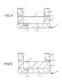
- the exposed portions 9 of the first insulator layer 1 are removed, in the manner as described above, to selectively expose regions of the substrate 2.
- the openings formed in the first insulator layer 1 are at least partial alignment with those formed in the second insulator layer 6.
- the openings in the first insulator layer 1 allow contact to be made to the pattern 4 in the substrate 2.
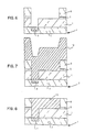
- the structure, as shown in Fig. 6, allows simultaneous formation of conductor material in the openings in the second insulator layer 6 (i.e., wiring channels) and in the openings in the first insulator layer 1 (i.e., stud vias).
- the structure, as shown in Fig. 6, is then subjected to a heating step so as to cure the polyimide layers 1 and 6.
- this step is carried out at a temperature of at least about 10 o C above the temperature at which the conductor material 10 is to be applied, as discussed below.
- this temperature is at least about 350 o C, and is usually within the range of about 350 o -450 o C, depending upon the conductor material 10 which is employed.
- the openings in the layers 1 and 6 are overfilled with conductor material 10, preferably metal, for example, aluminum, copper, Al-Cu, Al-Si or tungsten, preferably by physical vapor deposition, such as evaporation or sputtering, chemical vapor deposition or by plating.
- conductor material 10 preferably metal, for example, aluminum, copper, Al-Cu, Al-Si or tungsten, preferably by physical vapor deposition, such as evaporation or sputtering, chemical vapor deposition or by plating.
- the thickness of the conductor material 10 is at least as great as the combined thickness of the insulator layers 1 and 6 and the develop stop layer 5.
- the conductor material 10, which overlies the second insulating layer 6 is removed so as to coplanarize the surfaces of the conductor material 10 and the second insulator layer 6.
- a preferred method to accomplish this is by using chemical-mechanical polishing, as taught, for example, in Eur. Pat. Appln., No. 0,223,920, published Jun. 3, 1987, by Beyer, et al., the entire disclosure of which is incorporated herein by reference. That process involves the concurrent chemical and mechanical polishing of an overlying layer to expose the surface of a non-planar underlying layer on which it is formed, one layer of which is a conductive film, and the other, an insulator film.
- the process removes the overlying layer at a faster rate than the underlying layer, until the upper surface of the overlying layer becomes coplanar with that of the underlying layer.
- coplanarization can be accomplished by standard sacrificial planarization methods, such as etchback, as should be apparent to those skilled in the art.
- the conductor layer 10 is the final metal level of the semiconductor structure, a final passivation insulator is applied over the substrate. Otherwise, if additional levels of metallization are to be formed, then the steps as described above are repeated for each level desired.
- the first insulator layer 1 can be imagewise exposed in the second exposure step before the exposed portions of the develop stop layer 5 are removed. As noted above, however, it is generally preferred to first remove the exposed portions of the develop stop layer 5, since generally speaking this will provide a better exposure of the first insulator layer 1.
- a sample process flow for this embodiment, prior to application and planarization of metal, is as follows: Spin apply 0.1% 3-aminopropyltriethoxysilane (commercially available from Union Carbide under the designation "A1100") in methanol to a processed semiconductor substrate containing a pattern of metallization; Spin apply "PROBIMIDE 408" at 500 rpms, then hold at 4,000 rpms for 25 sec.; Bake at 80 o C for 20 min.; Apply Si by chemical vapor deposition; Spin apply "PROBIMIDE 408” and bake as above; Expose to UV light (270 mj at 365 nm); Develop second "PROBIMIDE 408" layer with a 45 sec.
- the present invention provides multi-level coplanar conductor/insulator films, by forming the desired channels and stud vias directly in the insulator layers, without the need for separate masking layers and image transfer steps. Accordingly, the need for resist stripping operations, which can damage the patterns formed in the insulator layers, is also avoided.
Abstract
Description
- This invention relates to the manufacture of VLSI semiconductor chips, and, more particularly, to a process for forming multi-level coplanar metal insulator films on a substrate.
- In the field of VLSI semiconductor chip processing, multi-level metal patterns are used to interconnect devices. One technique for accomplishing this is disclosed in IBM Tech. Discl. Bull., Vol. 25, No. 10 (Mar. 1983), pp. 5309-5314, where a first metal pattern is formed in an insulator layer. An insulator layer is deposited, and a series of holes are etched through this layer in locations where interconnections (or stud vias) are desired. The holes are filled with metal, and another insulator layer is deposited; this layer is patterned, and metal is deposited in these openings, thus making contact with the first metal pattern. This process is cumbersome and costly to carry out, however, as it involves several sequences of masking and etching steps.
- A simpler approach is shown in U.S. Pat. No. 4,789,648, issued to Chow, et al. on Dec. 6, 1988, which includes the following steps: depositing an insulator layer over an underlying insulator layer containing a metal pattern; applying an etch stop layer; defining holes in the etch stop; depositing another insulator layer; defining openings (or wiring channels) in the upper insulator layer in alignment with the holes in the etch stop; overfilling the channels and via holes with metal; and then removing the excess metal to form a coplanar metal/insulator surface. While this process is less complicated, nevertheless, it still involves two sequences of masking and etching steps to form the via holes and the wiring channels.
- Another conventional technique, known as the pillar process, is exemplified in U.S. Pat. No. 4,621,045, issued to Goodner on Nov. 4, 1986, in which a conductive pillar is provided in an insulator layer to connect two layers of metal. This process also has a high degree of complexity, however, with multiple masking and etching sequences.
- Now, in accordance with the present invention as claimed, there is provided a less cumbersome process, which employs insulator layers comprising a photosensitive polyimide polymer composition. Openings are formed directly in the insulator layers, without requiring the use of masking layers and pattern transfer steps. The openings which are in at least partial alignment are simultaneously filled with a conductor material, and the material which overlies the upper insulator layer is removed to achieve a coplanar conductor/insulator film. The process steps can be repeated to form additional coplanar conductor/insulator films.
- In a preferred embodiment, the process involves forming a multi-level coplanar conductor/insulator film on a substrate by first applying a first layer comprising a photosensitive polyimide polymer composition to the substrate. A develop stop layer is applied to the first layer, and a second layer comprising a photosensitive polyimide polymer composition is applied to the develop stop layer. The second layer is imagewise exposed and developed so as to selectively expose portions of the develop stop layer, and the exposed portions are removed. The first layer is imagewise exposed and developed so as to selectively expose regions of the substrate, the openings formed in the first layer being in alignment with at least a portion of the openings formed in the second layer. A conductor material is deposited on the second layer and in the openings in the first and second layers, and the conductor material which overlies the second layer is then removed to coplanarize the surfaces of the conductor material and the second layer.
- The foregoing and other objects, features and advantages of the invention will be apparent from the following more particular description of the preferred embodiments of the invention.
- Figs. 1-8 are cross-sectional views of a semiconductor structure illustrating the structure that results at various stages of the process of a preferred embodiment of the invention.
- Referring to Fig. 1, the process starts by applying a
first insulator layer 1 to a processed semiconductor substrate, indicated generally by thenumeral 2. Typically, thesubstrate 2 comprises aplanarized insulator layer 3 which includes a pattern ofconductor material 4. In general, theinsulator layer 3 is disposed over al integrated circuit chip, and theconductor material 4 is contact metallurgy to devices (not shown) formed in the chip. Preferably, thefirst insulator layer 1 is deposited over thesubstrate 2 by spin application, at about 2000 - 6000 rpm for about 20 - 60 seconds, and then baked at a temperature of about 70-90oC for about 10 - 30 minutes. It should be noted that it is also preferred, to improve adhesion, to apply a conventional adhesion promoter, such as 0.1% 3-aminopropyltriethoxysilane (commercially available from Union Carbide under the designation "A1100") in methanol, to the substrate before depositing thefirst insulator layer 1. In general, theplanarized insulator layer 3 commonly comprises silicon dioxide or reflowed phosphosilicate glass, and theconductor material 4 may be, for example, copper-doped aluminum or doped polycrystalline silicon. - Next, a relatively thin layer of develop
stop material 5, such as silicon, silicon dioxide, spin-on-glass or polysiloxane, is deposited over thefirst insulator layer 1. Then, asecond insulator layer 6 is deposited over the developstop layer 5, preferably under the conditions as described above for application of thefirst insulator layer 1. In general, thefirst insulator layer 1 is applied to a thickness typically ranging from about 0.2 - 1 microns, preferably from about 0.6 - 0.7 microns, while thesecond insulator layer 6 has a thickness usually ranging from about 0.05 - 1.2 microns, preferably from about 0.01 - 0.1 microns. As noted, the develop stop layer is relatively thin, having a thickness generally ranging from about 0.01 - 0.1 microns, preferably from about 0.025 - 0.05 microns. - It is an important feature of the invention, that both
insulator layers layers 
where R represents an aliphatic group, such as methyl, and R' represents an optional aliphatic substituent which may be the same as or different from R, and a suitable solvent for the polymer. (The R' substituent can enhance the photospeed or increase the Tg-value of the polymer.) Such photosensitive polyimide polymer compositions are disclosed in Pfeifer, et al., "Direct Photoimaging of Fully Imidized Solvent-Soluble Polyimides", Second International Conference on Polyimides, Mid-Hudson Section SPE, Ellenville, N.Y. (Oct. 30-Nov. 1, 1985), the entire disclosure of which is incorporated herein by reference. In a particularly preferred embodiment, the "PROBIMIDE 400" series, preferably "PROBIMIDE 408", commercially available from Ciba-Geigy Corp., is employed. - Referring to Fig. 2, the
second insulator layer 6 is exposed in a predetermined pattern to radiation, such as UV light, in a conventional fashion. During the exposure step it should be noted that thefirst insulator layer 1 is also exposed in the same pattern. In the preferred embodiment, bothinsulator layers stop layer 5 is selected of a material which is capable of transmitting radiation to theunderlying insulator layer 1 in the exposed areas. - Referring to Fig. 3, following the exposure step, portions of the
second insulator layer 6 are removed to selectively expose or reveal portions of the developstop layer 5. For example, when "PROBIMIDE 408" is used as the photosensitive polyimide polymer composition, theunexposed portions 8 of thesecond insulator layer 6 are removed, preferably by spraying with a conventional developer, such as, for example, gammabutylactone. In general, the development time will depend on the thickness of thesecond insulator layer 6, as well as other factors known to those skilled in the art. It should be noted that the developstop layer 5 serves to prevent development of the underlyingfirst insulator layer 1. - Referring to Fig. 4, the exposed portions of the develop
stop layer 5 are then removed, preferably with a wet chemical etchant, such as 20 wt. % KOH/2 vol. % isopropyl alcohol in water. However, dry etching techniques can also be employed, as should be apparent to those skilled in the art.
Referring to Fig. 5, thefirst insulator layer 1 is then exposed in a predetermined pattern to radiation, such as UV light, in a conventional manner. As with thesecond insulator layer 6, the exposedportions 9 of thefirst insulator layer 1 are removed, in the manner as described above, to selectively expose regions of thesubstrate 2. As shown in Fig. 6, the openings formed in thefirst insulator layer 1 are at least partial alignment with those formed in thesecond insulator layer 6. The openings in thefirst insulator layer 1 allow contact to be made to thepattern 4 in thesubstrate 2. The structure, as shown in Fig. 6, allows simultaneous formation of conductor material in the openings in the second insulator layer 6 (i.e., wiring channels) and in the openings in the first insulator layer 1 (i.e., stud vias). - The structure, as shown in Fig. 6, is then subjected to a heating step so as to cure the
polyimide layers conductor material 10 is to be applied, as discussed below. Typically, this temperature is at least about 350oC, and is usually within the range of about 350o-450oC, depending upon theconductor material 10 which is employed. - Next, as shown in Fig. 7, the openings in the
layers conductor material 10, preferably metal, for example, aluminum, copper, Al-Cu, Al-Si or tungsten, preferably by physical vapor deposition, such as evaporation or sputtering, chemical vapor deposition or by plating. It should be noted that the thickness of theconductor material 10 is at least as great as the combined thickness of the insulator layers 1 and 6 and thedevelop stop layer 5. - In the next step, as shown in Fig. 8, the
conductor material 10, which overlies the second insulatinglayer 6 is removed so as to coplanarize the surfaces of theconductor material 10 and thesecond insulator layer 6. A preferred method to accomplish this is by using chemical-mechanical polishing, as taught, for example, in Eur. Pat. Appln., No. 0,223,920, published Jun. 3, 1987, by Beyer, et al., the entire disclosure of which is incorporated herein by reference. That process involves the concurrent chemical and mechanical polishing of an overlying layer to expose the surface of a non-planar underlying layer on which it is formed, one layer of which is a conductive film, and the other, an insulator film. Using a polishing pad and a slurry, the process removes the overlying layer at a faster rate than the underlying layer, until the upper surface of the overlying layer becomes coplanar with that of the underlying layer. As another alternative, coplanarization can be accomplished by standard sacrificial planarization methods, such as etchback, as should be apparent to those skilled in the art. - If the
conductor layer 10 is the final metal level of the semiconductor structure, a final passivation insulator is applied over the substrate. Otherwise, if additional levels of metallization are to be formed, then the steps as described above are repeated for each level desired. - Various modifications can be made in the process, as will be apparent to those skilled in the art. For example, depending upon the choice of material for the
develop stop layer 5, thefirst insulator layer 1 can be imagewise exposed in the second exposure step before the exposed portions of thedevelop stop layer 5 are removed. As noted above, however, it is generally preferred to first remove the exposed portions of thedevelop stop layer 5, since generally speaking this will provide a better exposure of thefirst insulator layer 1. - A sample process flow for this embodiment, prior to application and planarization of metal, is as follows:
Spin apply 0.1% 3-aminopropyltriethoxysilane (commercially available from Union Carbide under the designation "A1100") in methanol to a processed semiconductor substrate containing a pattern of metallization;
Spin apply "PROBIMIDE 408" at 500 rpms, then hold at 4,000 rpms for 25 sec.;
Bake at 80oC for 20 min.;
Apply Si by chemical vapor deposition;
Spin apply "PROBIMIDE 408" and bake as above;
Expose to UV light (270 mj at 365 nm);
Develop second "PROBIMIDE 408" layer with a 45 sec. spray of gammabutylactone at 500 rpms;
Rinse with a 20 sec. spray of xylene at 500 rpms;
Dry with N₂;
Etch Si by immersion in 20 wt. % KOH/2 vol. % isopropyl alcohol in water;
Expose to UV light (270 mj at 365 nm);
Develop, rinse and dry as above; and
Ramp cure to 350oC. - As such, the present invention provides multi-level coplanar conductor/insulator films, by forming the desired channels and stud vias directly in the insulator layers, without the need for separate masking layers and image transfer steps. Accordingly, the need for resist stripping operations, which can damage the patterns formed in the insulator layers, is also avoided.
Claims (9)
- A process for forming multi-level coplanar conductor/insulator films on a substrate (2) having a conductor pattern (4), comprising the steps of:
applying a first layer (1) comprising a photosensitive polyimide polymer composition to said substrate;
applying a develop stop layer (5) to said first layer;
applying a second layer (6) comprising a photosensitive polyimide polymer composition to said develop stop layer;
imagewise exposing and developing said second layer so as to selectively expose portions of said develop stop layer;
removing said exposed portions of said develop stop layer;
imagewise exposing and developing said first layer so as to selectively expose regions of said substrate, the openings (9) formed in said first layer being in alignment with at least a portion of the openings (8) formed in said second layer;
depositing a conductor material (10) on said second layer and in said openings in said first and second layers; and
removing said conductor material which overlies said second layer to coplanarize the surfaces of conductor material and said second layer. - The process of Claim 1, wherein said steps are repeated to form additional coplanar conductor/insulator films.
- The process of Claim 1 or 2, wherein said photosensitive polyimide polymer composition comprises a fully imidized solvent soluble polyimide with a structural unit having the general formula

- The process of Claim 1, 2 or 3, wherein said develop stop layer comprises a material selected from silicon, silicon dioxide, spin-on-glass and a polysiloxane.
- The process of any one of the preceding claims, wherein said conductor is a metal selected from aluminum, copper, Al-Cu, Al-Si and tungsten.
- The process of any one of the preceding claims, wherein said first layer is imagewise exposed before said exposed portions of said develop stop layer are removed.
- The process of any one of the preceding claims wherein said first layer has a thickness ranging from about 0.2 to about 1 microns, preferably between 0,6 to 0,7 microns; and said second layer has a thickness ranging from about 0.05 to about 1.2 microns, preferably from 0,2 to 0,5 microns; and said develop stop layer has a thickness ranging from about 0.01 to about 0.1 microns, preferably between 0,025 to 0,05 microns.
- The process of any one of the preceding claims, wherein said conductor material which overlies said second layer is removed by using chemical-mechanical polishing.
- A semiconductor structure manufactured according to the process of any one of the preceding claims.
Applications Claiming Priority (2)
| Application Number | Priority Date | Filing Date | Title |
|---|---|---|---|
| US07/516,394 US5091289A (en) | 1990-04-30 | 1990-04-30 | Process for forming multi-level coplanar conductor/insulator films employing photosensitive polyimide polymer compositions |
| US516394 | 1990-04-30 |
Publications (3)
| Publication Number | Publication Date |
|---|---|
| EP0455031A2 true EP0455031A2 (en) | 1991-11-06 |
| EP0455031A3 EP0455031A3 (en) | 1992-04-22 |
| EP0455031B1 EP0455031B1 (en) | 1995-11-22 |
Family
ID=24055379
Family Applications (1)
| Application Number | Title | Priority Date | Filing Date |
|---|---|---|---|
| EP91105940A Expired - Lifetime EP0455031B1 (en) | 1990-04-30 | 1991-04-13 | Process for forming multi-level coplanar conductor/insulator films employing photosensitive polyimide polymer compositions |
Country Status (4)
| Country | Link |
|---|---|
| US (1) | US5091289A (en) |
| EP (1) | EP0455031B1 (en) |
| JP (1) | JPH0770594B2 (en) |
| DE (1) | DE69114759T2 (en) |
Cited By (5)
| Publication number | Priority date | Publication date | Assignee | Title |
|---|---|---|---|---|
| US5425337A (en) * | 1992-11-19 | 1995-06-20 | Izusu Ceramics Research Institute Co., Ltd. | Pre-chamber type engine |
| DE19614164A1 (en) * | 1995-10-19 | 1997-04-24 | Mitsubishi Electric Corp | Laminated connection on semiconductor substrate formation method for DRAM |
| FR2789804A1 (en) * | 1999-02-17 | 2000-08-18 | France Telecom | ANISOTROPIC GASEOUS PLASMA ENGRAVING PROCESS OF AN ORGANIC DIELECTRIC POLYMERIC MATERIAL AND APPLICATION TO MICROELECTRONICS |
| WO2000075979A1 (en) * | 1999-06-09 | 2000-12-14 | Alliedsignal Inc. | Process of using siloxane dielectric films in the integration of organic dielectric films in electronic devices |
| GB2356974A (en) * | 1999-08-30 | 2001-06-06 | Lucent Technologies Inc | Process for manufacturing a dual damascene structure for an integrated circuit using an etch stop layer |
Families Citing this family (25)
| Publication number | Priority date | Publication date | Assignee | Title |
|---|---|---|---|---|
| US5413966A (en) * | 1990-12-20 | 1995-05-09 | Lsi Logic Corporation | Shallow trench etch |
| US5290396A (en) * | 1991-06-06 | 1994-03-01 | Lsi Logic Corporation | Trench planarization techniques |
| US5217566A (en) * | 1991-06-06 | 1993-06-08 | Lsi Logic Corporation | Densifying and polishing glass layers |
| US5252503A (en) * | 1991-06-06 | 1993-10-12 | Lsi Logic Corporation | Techniques for forming isolation structures |
| US5225358A (en) * | 1991-06-06 | 1993-07-06 | Lsi Logic Corporation | Method of forming late isolation with polishing |
| US5248625A (en) * | 1991-06-06 | 1993-09-28 | Lsi Logic Corporation | Techniques for forming isolation structures |
| US5514616A (en) * | 1991-08-26 | 1996-05-07 | Lsi Logic Corporation | Depositing and densifying glass to planarize layers in semi-conductor devices based on CMOS structures |
| US5397863A (en) * | 1991-09-13 | 1995-03-14 | International Business Machines Corporation | Fluorinated carbon polymer composites |
| US5310622A (en) * | 1992-05-29 | 1994-05-10 | Sgs-Thomson Microelectronics, Inc. | Method of patterning a reflective surface in an integrated circuit |
| US5371047A (en) * | 1992-10-30 | 1994-12-06 | International Business Machines Corporation | Chip interconnection having a breathable etch stop layer |
| US5869175A (en) * | 1994-01-31 | 1999-02-09 | Stmicroelectronics, Inc. | Integrated circuit structure having two photoresist layers |
| US5486493A (en) * | 1994-02-25 | 1996-01-23 | Jeng; Shin-Puu | Planarized multi-level interconnect scheme with embedded low-dielectric constant insulators |
| US5888896A (en) * | 1996-06-27 | 1999-03-30 | Micron Technology, Inc. | Method for making an electrical contact to a node location and process for forming a conductive line or other circuit component |
| US6143640A (en) * | 1997-09-23 | 2000-11-07 | International Business Machines Corporation | Method of fabricating a stacked via in copper/polyimide beol |
| US6127721A (en) * | 1997-09-30 | 2000-10-03 | Siemens Aktiengesellschaft | Soft passivation layer in semiconductor fabrication |
| KR100252049B1 (en) * | 1997-11-18 | 2000-04-15 | 윤종용 | The atomic layer deposition method for fabricating aluminum layer |
| US6265780B1 (en) * | 1998-12-01 | 2001-07-24 | United Microelectronics Corp. | Dual damascene structure for the wiring-line structures of multi-level interconnects in integrated circuit |
| US6965165B2 (en) | 1998-12-21 | 2005-11-15 | Mou-Shiung Lin | Top layers of metal for high performance IC's |
| US6107006A (en) * | 1999-01-18 | 2000-08-22 | Winbond Electronics Corp. | Method for forming pattern |
| US6803327B1 (en) | 1999-04-05 | 2004-10-12 | Taiwan Semiconductor Manufacturing Company | Cost effective polymide process to solve passivation extrusion or damage and SOG delminates |
| US6387810B2 (en) * | 1999-06-28 | 2002-05-14 | International Business Machines Corporation | Method for homogenizing device parameters through photoresist planarization |
| US6882045B2 (en) * | 1999-10-28 | 2005-04-19 | Thomas J. Massingill | Multi-chip module and method for forming and method for deplating defective capacitors |
| US6428942B1 (en) * | 1999-10-28 | 2002-08-06 | Fujitsu Limited | Multilayer circuit structure build up method |
| US6869750B2 (en) * | 1999-10-28 | 2005-03-22 | Fujitsu Limited | Structure and method for forming a multilayered structure |
| US6798073B2 (en) * | 2001-12-13 | 2004-09-28 | Megic Corporation | Chip structure and process for forming the same |
Citations (1)
| Publication number | Priority date | Publication date | Assignee | Title |
|---|---|---|---|---|
| US4523976A (en) * | 1984-07-02 | 1985-06-18 | Motorola, Inc. | Method for forming semiconductor devices |
Family Cites Families (14)
| Publication number | Priority date | Publication date | Assignee | Title |
|---|---|---|---|---|
| EP0019391B1 (en) * | 1979-05-12 | 1982-10-06 | Fujitsu Limited | Improvement in method of manufacturing electronic device having multilayer wiring structure |
| JPS5850417B2 (en) * | 1979-07-31 | 1983-11-10 | 富士通株式会社 | Manufacturing method of semiconductor device |
| US4657832A (en) * | 1983-05-18 | 1987-04-14 | Ciba-Geigy Corporation | Photosensitive polymers as coating materials |
| US4629777A (en) * | 1983-05-18 | 1986-12-16 | Ciba-Geigy Corporation | Polyimides, a process for their preparation and their use |
| US4656116A (en) * | 1983-10-12 | 1987-04-07 | Ciba-Geigy Corporation | Radiation-sensitive coating composition |
| ATE37889T1 (en) * | 1984-06-29 | 1988-10-15 | Siemens Ag | THERMOSTABLE, RADIATION CROSSLINKABLE POLYMER SYSTEM BASED ON BISPHENOLS AND EPICHLORHYDRIN AND METHOD FOR ITS USE. |
| US4698295A (en) * | 1984-11-16 | 1987-10-06 | Ciba-Geigy Corporation | Polyimides, a process for their preparation and their use, and tetracarboxylic acids and tetracarboxylic acid derivatives |
| US4621045A (en) * | 1985-06-03 | 1986-11-04 | Motorola, Inc. | Pillar via process |
| US4665007A (en) * | 1985-08-19 | 1987-05-12 | International Business Machines Corporation | Planarization process for organic filling of deep trenches |
| US4786569A (en) * | 1985-09-04 | 1988-11-22 | Ciba-Geigy Corporation | Adhesively bonded photostructurable polyimide film |
| US4789648A (en) * | 1985-10-28 | 1988-12-06 | International Business Machines Corporation | Method for producing coplanar multi-level metal/insulator films on a substrate and for forming patterned conductive lines simultaneously with stud vias |
| US4944836A (en) * | 1985-10-28 | 1990-07-31 | International Business Machines Corporation | Chem-mech polishing method for producing coplanar metal/insulator films on a substrate |
| US4842991A (en) * | 1987-07-31 | 1989-06-27 | Texas Instruments Incorporated | Self-aligned nonnested sloped via |
| US4997746A (en) * | 1988-11-22 | 1991-03-05 | Greco Nancy A | Method of forming conductive lines and studs |
-
1990
- 1990-04-30 US US07/516,394 patent/US5091289A/en not_active Expired - Fee Related
-
1991
- 1991-03-29 JP JP3089343A patent/JPH0770594B2/en not_active Expired - Lifetime
- 1991-04-13 DE DE69114759T patent/DE69114759T2/en not_active Expired - Fee Related
- 1991-04-13 EP EP91105940A patent/EP0455031B1/en not_active Expired - Lifetime
Patent Citations (1)
| Publication number | Priority date | Publication date | Assignee | Title |
|---|---|---|---|---|
| US4523976A (en) * | 1984-07-02 | 1985-06-18 | Motorola, Inc. | Method for forming semiconductor devices |
Non-Patent Citations (4)
| Title |
|---|
| * abstract * * |
| * the whole document * * |
| IBM TECHNICAL DISCLOSURE BULLETIN. vol. 32, no. 10B, March 1990, NEW YORK US pages 114 - 115; 'Lithographic Patterns with a barrier layer' * |
| JOURNAL OF THE ELECTROCHEMICAL SOCIETY. vol. 137, no. 3, March 1990, MANCHESTER, NEW HAMPSHIRE US pages 961 - 966; K.K. CHAKRAVORTY ET.AL.: 'Photosensitive Polyimide as a Dielectric in High Density Thin Film Copper-Polyimide Interconnect Structures' * |
Cited By (8)
| Publication number | Priority date | Publication date | Assignee | Title |
|---|---|---|---|---|
| US5425337A (en) * | 1992-11-19 | 1995-06-20 | Izusu Ceramics Research Institute Co., Ltd. | Pre-chamber type engine |
| DE19614164A1 (en) * | 1995-10-19 | 1997-04-24 | Mitsubishi Electric Corp | Laminated connection on semiconductor substrate formation method for DRAM |
| DE19614164C2 (en) * | 1995-10-19 | 2000-10-26 | Mitsubishi Electric Corp | Method of forming a multilayer connection |
| FR2789804A1 (en) * | 1999-02-17 | 2000-08-18 | France Telecom | ANISOTROPIC GASEOUS PLASMA ENGRAVING PROCESS OF AN ORGANIC DIELECTRIC POLYMERIC MATERIAL AND APPLICATION TO MICROELECTRONICS |
| EP1030353A1 (en) * | 1999-02-17 | 2000-08-23 | France Telecom | Anisotropic plasma etching of a dielectric, organic polymer material |
| US6326302B1 (en) | 1999-02-17 | 2001-12-04 | France Telecom | Process for the anisotropic etching of an organic dielectric polymer material by a plasma gas and application in microelectronics |
| WO2000075979A1 (en) * | 1999-06-09 | 2000-12-14 | Alliedsignal Inc. | Process of using siloxane dielectric films in the integration of organic dielectric films in electronic devices |
| GB2356974A (en) * | 1999-08-30 | 2001-06-06 | Lucent Technologies Inc | Process for manufacturing a dual damascene structure for an integrated circuit using an etch stop layer |
Also Published As
| Publication number | Publication date |
|---|---|
| JPH0770594B2 (en) | 1995-07-31 |
| EP0455031B1 (en) | 1995-11-22 |
| DE69114759D1 (en) | 1996-01-04 |
| JPH04229638A (en) | 1992-08-19 |
| EP0455031A3 (en) | 1992-04-22 |
| DE69114759T2 (en) | 1996-06-20 |
| US5091289A (en) | 1992-02-25 |
Similar Documents
| Publication | Publication Date | Title |
|---|---|---|
| EP0455031B1 (en) | Process for forming multi-level coplanar conductor/insulator films employing photosensitive polyimide polymer compositions | |
| EP0455032B1 (en) | Process for forming multi-level coplanar conductor/insulator films employing photosensitive polyimide polymer compositions | |
| US7256136B2 (en) | Self-patterning of photo-active dielectric materials for interconnect isolation | |
| US6319821B1 (en) | Dual damascene approach for small geometry dimension | |
| JP2661652B2 (en) | Integrated circuit device having air-permeable etching-resistant layer and manufacturing method | |
| US7364836B2 (en) | Dual damascene process | |
| AU581110B2 (en) | Method for forming vertical interconnects in polyimide insulating layers | |
| KR20000016960A (en) | Prevention of photoresist poisoning from dielectric antireflective coating in semiconductor fabrication | |
| EP0370935B1 (en) | Method of forming conductive lines and studs | |
| US20060094204A1 (en) | Planarization material, anti-reflection coating material, and method for manufacturing semiconductor device thereby | |
| JP2003163265A (en) | Wiring structure and its manufacturing method | |
| JPH0669351A (en) | Manufacture of contact of multilayer metal interconnection structure | |
| US6803327B1 (en) | Cost effective polymide process to solve passivation extrusion or damage and SOG delminates | |
| JP2720023B2 (en) | Method for manufacturing semiconductor device | |
| JP2001345380A (en) | Semiconductor device and method of manufacturing the same | |
| JPH0750694B2 (en) | Conductive layer formation method | |
| JP2002270691A (en) | Wiring structure | |
| JPH06120219A (en) | Forming method of metal wiring | |
| KR100458594B1 (en) | Fabrication method of semiconductor device | |
| CA2039321A1 (en) | Process for forming multi-level coplanar conductor/insulator films employing photosensitive polyimide polymer compositions | |
| JP2002170882A (en) | Method for fabricating wiring structure | |
| JP3166912B2 (en) | Method for manufacturing semiconductor device | |
| KR100197124B1 (en) | Forming method for metal wiring in semiconductor divice | |
| JP2004040019A (en) | Method for forming metal wiring | |
| KR100365936B1 (en) | Method for forming via contact in semiconductor device |
Legal Events
| Date | Code | Title | Description |
|---|---|---|---|
| PUAI | Public reference made under article 153(3) epc to a published international application that has entered the european phase |
Free format text: ORIGINAL CODE: 0009012 |
|
| AK | Designated contracting states |
Kind code of ref document: A2 Designated state(s): DE FR GB IT |
|
| 17P | Request for examination filed |
Effective date: 19911219 |
|
| PUAL | Search report despatched |
Free format text: ORIGINAL CODE: 0009013 |
|
| AK | Designated contracting states |
Kind code of ref document: A3 Designated state(s): DE FR GB IT |
|
| 17Q | First examination report despatched |
Effective date: 19950123 |
|
| GRAA | (expected) grant |
Free format text: ORIGINAL CODE: 0009210 |
|
| AK | Designated contracting states |
Kind code of ref document: B1 Designated state(s): DE FR GB IT |
|
| PG25 | Lapsed in a contracting state [announced via postgrant information from national office to epo] |
Ref country code: IT Free format text: LAPSE BECAUSE OF FAILURE TO SUBMIT A TRANSLATION OF THE DESCRIPTION OR TO PAY THE FEE WITHIN THE PRESCRIBED TIME-LIMIT;WARNING: LAPSES OF ITALIAN PATENTS WITH EFFECTIVE DATE BEFORE 2007 MAY HAVE OCCURRED AT ANY TIME BEFORE 2007. THE CORRECT EFFECTIVE DATE MAY BE DIFFERENT FROM THE ONE RECORDED. Effective date: 19951122 |
|
| REF | Corresponds to: |
Ref document number: 69114759 Country of ref document: DE Date of ref document: 19960104 |
|
| ET | Fr: translation filed | ||
| PGFP | Annual fee paid to national office [announced via postgrant information from national office to epo] |
Ref country code: FR Payment date: 19960412 Year of fee payment: 6 |
|
| PG25 | Lapsed in a contracting state [announced via postgrant information from national office to epo] |
Ref country code: GB Effective date: 19960413 |
|
| PLBE | No opposition filed within time limit |
Free format text: ORIGINAL CODE: 0009261 |
|
| STAA | Information on the status of an ep patent application or granted ep patent |
Free format text: STATUS: NO OPPOSITION FILED WITHIN TIME LIMIT |
|
| 26N | No opposition filed | ||
| GBPC | Gb: european patent ceased through non-payment of renewal fee |
Effective date: 19960413 |
|
| PG25 | Lapsed in a contracting state [announced via postgrant information from national office to epo] |
Ref country code: FR Free format text: LAPSE BECAUSE OF NON-PAYMENT OF DUE FEES Effective date: 19971231 |
|
| REG | Reference to a national code |
Ref country code: FR Ref legal event code: ST |
|
| PGFP | Annual fee paid to national office [announced via postgrant information from national office to epo] |
Ref country code: DE Payment date: 19990421 Year of fee payment: 9 |
|
| PG25 | Lapsed in a contracting state [announced via postgrant information from national office to epo] |
Ref country code: DE Free format text: LAPSE BECAUSE OF NON-PAYMENT OF DUE FEES Effective date: 20010201 |