EP0468715B1 - Adiabatic reflection apparatus - Google Patents
Adiabatic reflection apparatus Download PDFInfo
- Publication number
- EP0468715B1 EP0468715B1 EP91306622A EP91306622A EP0468715B1 EP 0468715 B1 EP0468715 B1 EP 0468715B1 EP 91306622 A EP91306622 A EP 91306622A EP 91306622 A EP91306622 A EP 91306622A EP 0468715 B1 EP0468715 B1 EP 0468715B1
- Authority
- EP
- European Patent Office
- Prior art keywords
- waveguide
- mode
- branch
- common
- coupler
- Prior art date
- Legal status (The legal status is an assumption and is not a legal conclusion. Google has not performed a legal analysis and makes no representation as to the accuracy of the status listed.)
- Expired - Lifetime
Links
- 230000003287 optical effect Effects 0.000 claims description 17
- 239000006185 dispersion Substances 0.000 claims description 12
- 230000008878 coupling Effects 0.000 claims description 6
- 238000010168 coupling process Methods 0.000 claims description 6
- 238000005859 coupling reaction Methods 0.000 claims description 6
- 239000010409 thin film Substances 0.000 claims description 5
- VYPSYNLAJGMNEJ-UHFFFAOYSA-N Silicium dioxide Chemical compound O=[Si]=O VYPSYNLAJGMNEJ-UHFFFAOYSA-N 0.000 claims description 4
- 239000000377 silicon dioxide Substances 0.000 claims description 2
- 239000000758 substrate Substances 0.000 claims description 2
- 239000000969 carrier Substances 0.000 description 9
- 230000005540 biological transmission Effects 0.000 description 7
- 230000010363 phase shift Effects 0.000 description 5
- 230000003321 amplification Effects 0.000 description 3
- 239000000835 fiber Substances 0.000 description 3
- 238000010438 heat treatment Methods 0.000 description 3
- 238000000034 method Methods 0.000 description 3
- 238000003199 nucleic acid amplification method Methods 0.000 description 3
- 230000007704 transition Effects 0.000 description 3
- XUIMIQQOPSSXEZ-UHFFFAOYSA-N Silicon Chemical compound [Si] XUIMIQQOPSSXEZ-UHFFFAOYSA-N 0.000 description 2
- 230000008859 change Effects 0.000 description 2
- 238000006243 chemical reaction Methods 0.000 description 2
- 230000001419 dependent effect Effects 0.000 description 2
- 230000000694 effects Effects 0.000 description 2
- 238000004519 manufacturing process Methods 0.000 description 2
- 239000013307 optical fiber Substances 0.000 description 2
- 229910052710 silicon Inorganic materials 0.000 description 2
- 239000010703 silicon Substances 0.000 description 2
- 230000001186 cumulative effect Effects 0.000 description 1
- 230000001934 delay Effects 0.000 description 1
- 230000001066 destructive effect Effects 0.000 description 1
- 238000006073 displacement reaction Methods 0.000 description 1
- 238000005516 engineering process Methods 0.000 description 1
- 238000003780 insertion Methods 0.000 description 1
- 230000037431 insertion Effects 0.000 description 1
- 230000010287 polarization Effects 0.000 description 1
- 230000008569 process Effects 0.000 description 1
- 230000005855 radiation Effects 0.000 description 1
Images

Classifications
-
- G—PHYSICS
- G02—OPTICS
- G02B—OPTICAL ELEMENTS, SYSTEMS OR APPARATUS
- G02B6/00—Light guides; Structural details of arrangements comprising light guides and other optical elements, e.g. couplings
- G02B6/24—Coupling light guides
- G02B6/26—Optical coupling means
- G02B6/28—Optical coupling means having data bus means, i.e. plural waveguides interconnected and providing an inherently bidirectional system by mixing and splitting signals
- G02B6/293—Optical coupling means having data bus means, i.e. plural waveguides interconnected and providing an inherently bidirectional system by mixing and splitting signals with wavelength selective means
- G02B6/29304—Optical coupling means having data bus means, i.e. plural waveguides interconnected and providing an inherently bidirectional system by mixing and splitting signals with wavelength selective means operating by diffraction, e.g. grating
- G02B6/29316—Light guides comprising a diffractive element, e.g. grating in or on the light guide such that diffracted light is confined in the light guide
- G02B6/29317—Light guides of the optical fibre type
- G02B6/29319—With a cascade of diffractive elements or of diffraction operations
-
- G—PHYSICS
- G01—MEASURING; TESTING
- G01D—MEASURING NOT SPECIALLY ADAPTED FOR A SPECIFIC VARIABLE; ARRANGEMENTS FOR MEASURING TWO OR MORE VARIABLES NOT COVERED IN A SINGLE OTHER SUBCLASS; TARIFF METERING APPARATUS; MEASURING OR TESTING NOT OTHERWISE PROVIDED FOR
- G01D5/00—Mechanical means for transferring the output of a sensing member; Means for converting the output of a sensing member to another variable where the form or nature of the sensing member does not constrain the means for converting; Transducers not specially adapted for a specific variable
- G01D5/26—Mechanical means for transferring the output of a sensing member; Means for converting the output of a sensing member to another variable where the form or nature of the sensing member does not constrain the means for converting; Transducers not specially adapted for a specific variable characterised by optical transfer means, i.e. using infrared, visible, or ultraviolet light
- G01D5/268—Mechanical means for transferring the output of a sensing member; Means for converting the output of a sensing member to another variable where the form or nature of the sensing member does not constrain the means for converting; Transducers not specially adapted for a specific variable characterised by optical transfer means, i.e. using infrared, visible, or ultraviolet light using optical fibres
-
- G—PHYSICS
- G02—OPTICS
- G02B—OPTICAL ELEMENTS, SYSTEMS OR APPARATUS
- G02B6/00—Light guides; Structural details of arrangements comprising light guides and other optical elements, e.g. couplings
- G02B6/10—Light guides; Structural details of arrangements comprising light guides and other optical elements, e.g. couplings of the optical waveguide type
- G02B6/12—Light guides; Structural details of arrangements comprising light guides and other optical elements, e.g. couplings of the optical waveguide type of the integrated circuit kind
- G02B6/12007—Light guides; Structural details of arrangements comprising light guides and other optical elements, e.g. couplings of the optical waveguide type of the integrated circuit kind forming wavelength selective elements, e.g. multiplexer, demultiplexer
-
- G—PHYSICS
- G02—OPTICS
- G02B—OPTICAL ELEMENTS, SYSTEMS OR APPARATUS
- G02B6/00—Light guides; Structural details of arrangements comprising light guides and other optical elements, e.g. couplings
- G02B6/10—Light guides; Structural details of arrangements comprising light guides and other optical elements, e.g. couplings of the optical waveguide type
- G02B6/12—Light guides; Structural details of arrangements comprising light guides and other optical elements, e.g. couplings of the optical waveguide type of the integrated circuit kind
- G02B6/122—Basic optical elements, e.g. light-guiding paths
- G02B6/125—Bends, branchings or intersections
-
- G—PHYSICS
- G02—OPTICS
- G02B—OPTICAL ELEMENTS, SYSTEMS OR APPARATUS
- G02B6/00—Light guides; Structural details of arrangements comprising light guides and other optical elements, e.g. couplings
- G02B6/24—Coupling light guides
- G02B6/26—Optical coupling means
- G02B6/28—Optical coupling means having data bus means, i.e. plural waveguides interconnected and providing an inherently bidirectional system by mixing and splitting signals
- G02B6/293—Optical coupling means having data bus means, i.e. plural waveguides interconnected and providing an inherently bidirectional system by mixing and splitting signals with wavelength selective means
- G02B6/29346—Optical coupling means having data bus means, i.e. plural waveguides interconnected and providing an inherently bidirectional system by mixing and splitting signals with wavelength selective means operating by wave or beam interference
- G02B6/2935—Mach-Zehnder configuration, i.e. comprising separate splitting and combining means
- G02B6/29352—Mach-Zehnder configuration, i.e. comprising separate splitting and combining means in a light guide
- G02B6/29355—Cascade arrangement of interferometers
-
- H—ELECTRICITY
- H04—ELECTRIC COMMUNICATION TECHNIQUE
- H04B—TRANSMISSION
- H04B10/00—Transmission systems employing electromagnetic waves other than radio-waves, e.g. infrared, visible or ultraviolet light, or employing corpuscular radiation, e.g. quantum communication
- H04B10/25—Arrangements specific to fibre transmission
- H04B10/2507—Arrangements specific to fibre transmission for the reduction or elimination of distortion or dispersion
- H04B10/2513—Arrangements specific to fibre transmission for the reduction or elimination of distortion or dispersion due to chromatic dispersion
- H04B10/2519—Arrangements specific to fibre transmission for the reduction or elimination of distortion or dispersion due to chromatic dispersion using Bragg gratings
-
- H—ELECTRICITY
- H04—ELECTRIC COMMUNICATION TECHNIQUE
- H04B—TRANSMISSION
- H04B10/00—Transmission systems employing electromagnetic waves other than radio-waves, e.g. infrared, visible or ultraviolet light, or employing corpuscular radiation, e.g. quantum communication
- H04B10/25—Arrangements specific to fibre transmission
- H04B10/2581—Multimode transmission
-
- G—PHYSICS
- G02—OPTICS
- G02B—OPTICAL ELEMENTS, SYSTEMS OR APPARATUS
- G02B6/00—Light guides; Structural details of arrangements comprising light guides and other optical elements, e.g. couplings
- G02B6/10—Light guides; Structural details of arrangements comprising light guides and other optical elements, e.g. couplings of the optical waveguide type
- G02B6/12—Light guides; Structural details of arrangements comprising light guides and other optical elements, e.g. couplings of the optical waveguide type of the integrated circuit kind
- G02B2006/12083—Constructional arrangements
- G02B2006/12107—Grating
-
- G—PHYSICS
- G02—OPTICS
- G02B—OPTICAL ELEMENTS, SYSTEMS OR APPARATUS
- G02B6/00—Light guides; Structural details of arrangements comprising light guides and other optical elements, e.g. couplings
- G02B6/10—Light guides; Structural details of arrangements comprising light guides and other optical elements, e.g. couplings of the optical waveguide type
- G02B6/12—Light guides; Structural details of arrangements comprising light guides and other optical elements, e.g. couplings of the optical waveguide type of the integrated circuit kind
- G02B2006/12133—Functions
- G02B2006/12159—Interferometer
Definitions
- This invention relates to optical apparatus which operates selectively on optical signals based on the frequency content of the signal.
- the invention relates to optical filters, channel balancers and dispersion compensators.
- WDM wavelength division multiplexing
- wavelength dispersion that is, systems which utilize a dispersive transmission medium, such as a standard 1.5 ⁇ m optical fiber, cause optical radiation of different wavelengths to travel at different velocities. Consequently, a digital pulse tends to spread out as it propagates, thereby limiting the bit rate of the digital system. While numerous techniques have been proposed for addressing dispersion, including the use of single frequency lasers and/or dispersion shifted fiber, the problem remains.
- Reflective apparatus according to the invention is set out in claim 1.
- adiabatic reflection apparatus comprises a wavelength selective structure coupled to an adiabatic Y-coupler having single mode branches coupled to a multimode common section which supports both symmetric and anti-symmetric modes.
- One branch of the coupler converts guided light to a symmetric mode in the common section whereas the other branch converts guided light to an anti-symmetric mode in the common section.
- the wavelength selective structure includes at least two single mode optical waveguide arms, one end of each arm being coupled to the common section, and a reflection device (e.g., a grating) located in each arm. During reflection this structure converts guided light from a symmetric to an anti-symmetric mode and conversely.
- the amplitude of the channel carriers be maintained relatively balanced.
- This function is performed by applying the WDM signal to one branch of the Y-coupler and by designing the wavelength selective structure to reflect guided light at the wavelengths of each channel carrier to be balanced.
- the amplitudes of these channel carriers are sensed at the output of the other branch of the same coupler and are compared to one another (or to some standard reference), and any difference is used to generate an error signal.
- the latter is fed back to control elements which shift the reflection wavelengths of selected reflection devices, thereby altering the amount of energy reflected versus the amount transmitted.
- This controllable attenuation of the channel carriers enables their amplitudes to be balanced at one or more points (e.g., amplifier stages) along the transmission path.
- a pulse to be reshaped is applied to one branch of the Y-coupler.
- the wavelength selective structure includes a plurality of reflection devices tuned to different wavelengths (e.g., chirped gratings) so as to compensate for the dispersion.
- the reflected pulse is thereby reshaped and exits the other branch of the Y-coupler.
- the process may be reversed by applying the pulse first to the compensator to pre-distort its shape and then applying it to the dispersive medium.
- a second adiabatic Y-coupler is coupled through a second common section to the other ends of the waveguide arms of the wavelength selective structure.
- a WDM symmetric mode signal is applied to one branch of one coupler, and the selective structure is designed to reflect guided light of wavelength ⁇ r , where ⁇ r is the wavelength of the channel carrier to be selected in the channel dropping function. That channel carrier is reflected out through the anti-symmetric mode branch of the same coupler.
- the transmitted channel carriers exit the symmetric mode branch of the other coupler.
- an adiabatic reflection apparatus 10 comprising a wavelength selective structure 12 coupled to an adiabatic Y-coupler 14 having single mode branches 14.1 and 14.2 and a multimode common section 13.
- Variations of much of the apparatus of FIG. 1 are used in the dispersion compensator of FIG. 5 and the WDM channel balancer of FIG. 6.
- other applications such as a WDM channel dropping filter, may also include a second adiabatic Y-coupler 16 having single mode branches 16.1 and 16.2 coupled to structure 12 via a second multimode common section 15.
- a preferred mode of implementation utilizes silicon optical bench technology in which thin film silica waveguides are formed on a silicon substrate 18 as described by C. H. Henry and R. A. Levy in U. S. Patent No. 4,902,086.
- the couplers 14 and 16 are "adiabatic" in the sense defined by C. H. Henry et al in U. S. Patent No. 4,998,793. Briefly, a coupler is said to be adiabatic if the mode occupation (i.e., the energy in each mode) is conserved in passing through the coupler. To be adiabatic the transition in any waveguide parameter (e.g., width, thickness, refractive index) in passing through the coupler must be gradual, not abrupt. In an ideal adiabatic transition, any perturbation in a waveguide parameter is sufficiently gradual that no coupling occurs between optical modes having a difference in propagation constants ⁇ .
- mode occupation i.e., the energy in each mode
- any waveguide parameter e.g., width, thickness, refractive index
- the couplers 14 and 16 are each designed so that waveguide branchs 14.1, 16.1 convert guided light to a symmetric mode in the common sections 13 and 15, respectively, and the other branches 14.2, 16.2 convert guided light to an anti-symmetric mode in the common sections 13 and 15, respectively.
- One way to achieve this kind of mode conversion is to design waveguide branches 14.1, 16.1 to have higher effective refractive indices than waveguide branches 14.2, 16.2, which in turn is implemented in FIG. 1 by making waveguide branches 14.1, 16.1 wider than waveguide branches 14.2, 16.2 (W1>W2). In this sense, couplers 14 and 16 can be said to be asymmetric.
- structure 12 includes a plurality, in this case two, of single mode waveguide arms 12.1 and 12.2 connected in parallel with one another via symmetric adiabatic couplers 12.3 and 12.4.
- Structure 12 also includes reflection devices 20.1 and 20.2 located respectively in each arm and designed so that at least one predetermined wavelength ⁇ r is reflected whereas other wavelengths are transmitted.
- the devices are optical gratings made preferably by the technique described by T. Jewell et al in U.S. Patent No. 4,947,413.
- the waveguide arms and the reflection devices are mutually adapted to convert reflected light at ⁇ r from a symmetric mode to an anti-symmetric mode and conversely.
- the optical path lengths through arms 12.1 and 12.2 should differ by ⁇ r /4 or an odd multiple thereof, where ⁇ r is the wavelength as measured in the waveguide.
- the displacement a/2 is exaggerated in the interests of clarity of illustration.
- the gratings are unshifted and the physical length of waveguide arm 12.2' is made sufficiently longer (i.e., by a/2 or equivalently ⁇ r /4, or an odd multiple thereof) than that of arm 12.1' to introduce the desired phase shift.
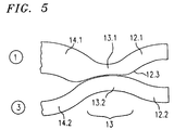
- the common sections 13 and 15 of FIGs. 1-3 are shown as being single multimode waveguides. However, each of them is preferrably constructed from physically separate, but optically coupled single mode waveguides. As shown in FIG. 5, common section 13 comprises two coupled single mode waveguides 13.1 and 13.2 which connect, respectively, waveguide branches 14.1, 14.2 to waveguide arms 12.1, 12.2. Illustratively, 4-7 ⁇ m wide cores of waveguides 13.1 and 13.2 are separated by about a 2 ⁇ m gap.
- branches 14.1, 14.2 adiabatically taper into waveguides 13.1, 13.2, and the latter are essentially identical to one another at least at the input to symmetric Y-coupler 12.3.
- waveguides 13.1, 13.2 together support both symmetric and antisymmetric modes. We have found that, from a processing standpoint, this embodiment facilitates the fabrication of an adiabatic transition between the waveguide branches 14.1, 14.2 and common section 13.
- a WDM signal having illustratively three channels with carriers designed ⁇ 1, ⁇ 2, ⁇ 3 in FIG. 1, is applied to port 1 of adiabatic reflection apparatus 10.
- the WDM signal excites the fundamental mode M o (FIG. 2) in single mode waveguide branch 14.1. This mode becomes a symmetric mode M s in common section 13.
- the mode M s splits into two fundamental modes M o1 and M o2 in single mode arms 12.1 and 12.2, respectively.
- Mode M o1 is incident upon grating 20.1 at plane 30 which reflects ⁇ 2 but transmits ⁇ 1 and ⁇ 3.
- mode M o2 is incident upon grating 20.2 at plane 40 which again reflects ⁇ 2, but in doing so it propagates an additional distance of a/2 which corresponds to a quarter wave phase shift. After being reflected, the mode M o2 at ⁇ 2 propagates back yet another distance of a/2 in order to reach plane 30. Thus, mode M o2 experiences a total of a half wave phase shift (180°) which is shown by the inverted mode M o3 in FIG. 2.
- M o1 and M o3 both at ⁇ 2, combine in section 13, as shown in FIG. 3, they form anti-symmetric mode M as at ⁇ 2 which propagates through single mode waveguide 14.2 and exits port 3 as fundamental mode M o4 .
- Channel carrier ⁇ 2 is thereby effectively filtered out of the WDM signal.
- the other channel carriers are not reflected by the gratings and, therefore, continue through structure 12 to coupler 16 as symmetric mode signals. They both, therefore, exit port 4 via branch 16.1 which, as noted earlier, is a symmetric mode waveguide.
- a plurality of filters may be connected in tandem; for example, port 4 of a first filter would be coupled to port 1 of a downstream second filter. Port 2 of the first filter would carry one dropped channel, whereas port 2 of the second filter would carry the other dropped channel.
- FIG. 6 Another application of the invention is shown in FIG. 6 where a pulse 72 of a digital signal propagates through a dispersive medium 70 causing it to alter its shape (e.g., spread out) as shown by pulse 74.
- This broadening is due to the change in propagation time (delay ⁇ ) with wavelength d ⁇ /d ⁇ .
- the pulse 74 is applied to branch 14.1 of an adiabatic coupler 14 of the type described in conjunction with FIGs. 1-5.
- wavelength selective structure 12" includes chirped gratings 40 and 50 in arms 12.1" and 12.2", respectively.
- gratings 40 and 50 may comprise a plurality of discrete gratings each reflective at a different wavelength covering a range of wavelengths expected to exist in pulse 74 so as to approximate continuous chirping.
- the effect of the chirped gratings is to vary the delay occurring in Bragg reflection with wavelength (-d ⁇ /d ⁇ ) which will cancel the (+d ⁇ /d ⁇ ) caused by fiber dispersion.
- Either form of grating will be considered herein to be chirped, and in either case the grating period a varies by such a small amount (e.g., 10 ⁇ 3 from one end to the other of a chirped grating) over the desired wavelength range, that simply using a shift essentially equal to a to design the grating will suffice.
- the gratings and waveguide arms are designed to convert reflected light from a symmetric mode to an anti-symmetric mode and conversely.
- the chirped gratings reflect the various wavelength components of pulse 74 with different delays in such a way that essentially the original pulse shape 72' is recovered at branch 14.2 of coupler 14.
- Pulse 72' is applied to utilization device 80. Note in this embodiment that only a single coupler 14 is necessary and waveguide arms 12.1 " and 12.2" need not be terminated. Also, additional compensation may be had by coupling branch 14.2 to another compensation device of the type just described. Depending on system considerations, such as insertion loss and the required dispersion compensation, a plurality of compensators may thus be connected in tandem.
- the embodiment of FIG. 6 positions the dispersion compensator after the dispersive medium 70, it is readily possible to position it before medium 70.
- the pulse shape is first altered (e.g., broadened by -d ⁇ /d ⁇ ) prior to entering medium 70 and then, after being further altered by medium 70 (e.g., compressed), the desired pulse shape is attained.
- the channels may be designed to be balanced at the transmitter, any wavelength or polarization dependent components (e.g., connectors, isolators, amplifiers) can create an imbalance.
- any wavelength or polarization dependent components e.g., connectors, isolators, amplifiers
- FIG. 7 another embodiment of the invention balances the channels by applying the WDM signal ⁇ 1 (A1), ⁇ 2(A2) to one branch 14.1 of asymmetric adiabatic coupler 14 and by designing the wavelength selective structure 12"' to reflect guided light at the wavelengths ⁇ 1 and ⁇ 2 of the carriers to be balanced.
- Structure 12 includes gratings 20.1, 20.2 which reflect at ⁇ 1 and gratings 20.3, 20.4 which reflect at ⁇ 2.
- elements 12.5 and 12.6 In proximity to the gratings are elements 12.5 and 12.6, (illustratively thin film heating elements overlying the gratings) for altering the refractive index (and hence the reflection wavelength) of the gratings.
- Elements 12.5 and 12.6 are controlled by feedback signals derived from sensor means 90 (including any necessary electronic circuitry) which senses the amplitude of guided light in branch 14.2 of coupler 14.
- carrier ⁇ 1(A1) is reflected by gratings 20.1, 20.2 and carrier ⁇ 2(A2) is reflected by gratings 20.3, 20.4, in the manner previously described in conjunction with FIGs. 1-4.
- the reflected signal ⁇ 1(A1), ⁇ 2(A2) exits through branch 14.2 where the difference, if any, between amplitudes A1 and A2 is sensed by sensor means 90. Any such difference causes sensor means 90 to generate an error signal which is fed back to elements 12.4 and 12.6 to alter the refractive index of the gratings. This change in turn alters the amount of energy at ⁇ 1 relative to that at ⁇ 2 which is reflected by the gratings versus that which is transmitted.
- This controllable attenuation of ⁇ 1 or ⁇ 2 or both continues until the two channels are balanced; i.e., until their amplitudes are essentially equal to A as depicted by the signals ⁇ 1(A), ⁇ 2(A) on branch 14.2.
- this balancing function could be performed at one or more of those stages.
- FIG. 7 shows Bragg reflection R plotted against wavelength ⁇ for two cases: curve one labeled "cold” to signify that either no heat is generated by element 12.5 of FIG. 6 or less heat is generated by element 12.5 than for curve II of FIG. 7 which is labeled "hot”. Note that heating the gratings causes curve II to shift to longer wavelengths.
- FIGs. 1-4 and 6 may be replaced with well-known resonant optical reflectors (RORs) of the type described for example, by R. Kazarinov et al in IEEE Journal of Quantum Electronics , 23, No. 9, p,1419 (1987) and C. H. Henry et al in IEEE Joumal of Quantum Electronics , 23, No. 9, p.1426 (1987).
- RORs resonant optical reflectors
Description
- This invention relates to optical apparatus which operates selectively on optical signals based on the frequency content of the signal. Illustratively, the invention relates to optical filters, channel balancers and dispersion compensators.
- One architecture for optical transmission systems, known as wavelength division multiplexing (WDM), involves assigning a different wavelength to each of a plurality of signal channels. At certain terminals or stations of a WDM system it is necessary to select a particular channel and separate it from the others. This function is performed by what is commonly known as a channel dropping filter.
- D. C. Johnson et al, Electronic Letters, Vol. 23, p.668 (1987) have proposed such a filter or tap based upon the use of an optical grating in each of a pair of parallel optical fiber (or integrated-optic) arms disposed between a pair of 3dB couplers. The fiber arms are supposed to be of equal length and the gratings are supposed to be in registration with one another so as to introduce no phase shift between different modes. In contrast, the 3dB couplers themselves introduce a 90° phase shift. Consequently, as shown in FIG. 1 of the article, reflected light λo traverses paths 1 and 2, undergoes constructive interference and exits port B. However, any light attempting to exit port A would experience destructive interference. This design is difficult to manufacture because the performance of this type of coupler is critically dependent on the length of the coupling region. If the length is not ideal, then the filter may exhibit undesirably high levels of back-reflected power and low levels of transmitted power. This problem is exacerbated if the filters are cascaded because the losses are cumulative.
- R. C. Alferness et al, Electronic Letters, Vol. 24, No. 3, pp. 150-151 (1988) describe an integrated optic version of the Johnson filter implemented in InP/InGaAsP. They point out that careful alignment of the gratings is critical to insure equal path lengths over the two grating arms. Otherwise, some of the light at λo will be reflected back into the incident waveguide (waveguide A of Johnson et al; upper left waveguide of Alferness et al).
- Another problem associated with many optical transmission systems is wavelength dispersion; that is, systems which utilize a dispersive transmission medium, such as a standard 1.5 µm optical fiber, cause optical radiation of different wavelengths to travel at different velocities. Consequently, a digital pulse tends to spread out as it propagates, thereby limiting the bit rate of the digital system. While numerous techniques have been proposed for addressing dispersion, including the use of single frequency lasers and/or dispersion shifted fiber, the problem remains.
- Reflective apparatus according to the invention is set out in
claim 1. - In accordance with one aspect of the invention, adiabatic reflection apparatus comprises a wavelength selective structure coupled to an adiabatic Y-coupler having single mode branches coupled to a multimode common section which supports both symmetric and anti-symmetric modes. One branch of the coupler converts guided light to a symmetric mode in the common section whereas the other branch converts guided light to an anti-symmetric mode in the common section. The wavelength selective structure includes at least two single mode optical waveguide arms, one end of each arm being coupled to the common section, and a reflection device (e.g., a grating) located in each arm. During reflection this structure converts guided light from a symmetric to an anti-symmetric mode and conversely.
- In one embodiment of the invention for use in WDM systems, particularly those involving long haul transmission and plural optical amplification stages, it is desirable that the amplitude of the channel carriers be maintained relatively balanced. This function is performed by applying the WDM signal to one branch of the Y-coupler and by designing the wavelength selective structure to reflect guided light at the wavelengths of each channel carrier to be balanced. The amplitudes of these channel carriers are sensed at the output of the other branch of the same coupler and are compared to one another (or to some standard reference), and any difference is used to generate an error signal. The latter is fed back to control elements which shift the reflection wavelengths of selected reflection devices, thereby altering the amount of energy reflected versus the amount transmitted. This controllable attenuation of the channel carriers enables their amplitudes to be balanced at one or more points (e.g., amplifier stages) along the transmission path.
- In another embodiment for use in a digital system with a dispersive transmission medium, a pulse to be reshaped is applied to one branch of the Y-coupler. The wavelength selective structure includes a plurality of reflection devices tuned to different wavelengths (e.g., chirped gratings) so as to compensate for the dispersion. The reflected pulse is thereby reshaped and exits the other branch of the Y-coupler. Alternatively, the process may be reversed by applying the pulse first to the compensator to pre-distort its shape and then applying it to the dispersive medium.
- In yet another embodiment of the invention for operation as a channel dropping filter in a WDM system, a second adiabatic Y-coupler is coupled through a second common section to the other ends of the waveguide arms of the wavelength selective structure. A WDM symmetric mode signal is applied to one branch of one coupler, and the selective structure is designed to reflect guided light of wavelength λr, where λr is the wavelength of the channel carrier to be selected in the channel dropping function. That channel carrier is reflected out through the anti-symmetric mode branch of the same coupler. The transmitted channel carriers, on the other hand, exit the symmetric mode branch of the other coupler.
- Advantageously, the absence of a critical coupling length will make the invention more easily manufacturable, with lower attendant cost, than the prior art designs discussed above.
- The invention, together with its various features and advantages can be readily understood from the following more detailed description taken in conjunction with the accompanying drawing, in which:
- FIG. 1 is a schematic top view of one embodiment of an adiabatic reflection filter of the invention implemented in substrate-supported thin film waveguides with staggered optical gratings as the reflection devices;
- FIGs. 2-3 show portions of FIG. 1 used in explaining the relationship between the symmetric/anti-symmetric modes and the reflection characteristics of the gratings;
- FIG. 4 is a schematic top view of a wavelength selective structure in which the gratings need not be staggered; instead waveguide arms of different lengths are used;
- FIG. 5 is a schematic top view of a portion of an embodiment of the invention in which the common section comprises two physically separate, but optically coupled waveguides;
- FIG. 6 is a schematic view of a dispersion compensator in accordance with another aspect of the invention;
- FIG. 7 is a schematic view of a channel balancing apparatus in accordance with still another aspect of the invention; and
- FIG. 8 shows the Bragg reflection curves used in describing how a single pair of gratings can be used to balance two channels of a WDM system.
- Turning now to FIG. 1, there is shown an
adiabatic reflection apparatus 10 comprising a wavelengthselective structure 12 coupled to an adiabatic Y-coupler 14 having single mode branches 14.1 and 14.2 and a multimodecommon section 13. - Variations of much of the apparatus of FIG. 1 are used in the dispersion compensator of FIG. 5 and the WDM channel balancer of FIG. 6. However, other applications, such as a WDM channel dropping filter, may also include a second adiabatic Y-
coupler 16 having single mode branches 16.1 and 16.2 coupled tostructure 12 via a second multimodecommon section 15. - The arrangements depicted illustrate implementation as substrate-supported thin film waveguides. A preferred mode of implementation utilizes silicon optical bench technology in which thin film silica waveguides are formed on a
silicon substrate 18 as described by C. H. Henry and R. A. Levy in U. S. Patent No. 4,902,086. - The
couplers - In addition to being adiabatic, the
couplers common sections common sections couplers - On the other hand,
structure 12 includes a plurality, in this case two, of single mode waveguide arms 12.1 and 12.2 connected in parallel with one another via symmetric adiabatic couplers 12.3 and 12.4.Common sections asymmetric couplers Structure 12 also includes reflection devices 20.1 and 20.2 located respectively in each arm and designed so that at least one predetermined wavelength λr is reflected whereas other wavelengths are transmitted. Illustratively, the devices are optical gratings made preferably by the technique described by T. Jewell et al in U.S. Patent No. 4,947,413. In addition, the waveguide arms and the reflection devices are mutually adapted to convert reflected light at λr from a symmetric mode to an anti-symmetric mode and conversely. To achieve this mode conversion the optical path lengths through arms 12.1 and 12.2 should differ by λr/4 or an odd multiple thereof, where λr is the wavelength as measured in the waveguide. In FIG. 1 this quarter wavelength shift is implemented by using waveguide arms of the same physical length and by introducing a grating shift of a/2 (or an odd multiple thereof), where a is the grating period (a=λr/2 for first order Bragg reflection); that is, the gratings are displaced from one another by an axial distance (in the direction of light propagation) of about a/2. Once again, in FIG. 2 the displacement a/2 is exaggerated in the interests of clarity of illustration. Alternatively, as shown in FIG. 4, the gratings are unshifted and the physical length of waveguide arm 12.2' is made sufficiently longer (i.e., by a/2 or equivalently λr/4, or an odd multiple thereof) than that of arm 12.1' to introduce the desired phase shift. - The
common sections common section 13 comprises two coupled single mode waveguides 13.1 and 13.2 which connect, respectively, waveguide branches 14.1, 14.2 to waveguide arms 12.1, 12.2. Illustratively, 4-7 µm wide cores of waveguides 13.1 and 13.2 are separated by about a 2 µm gap. One feature of this configuration is that branches 14.1, 14.2 adiabatically taper into waveguides 13.1, 13.2, and the latter are essentially identical to one another at least at the input to symmetric Y-coupler 12.3. Like thecommon section 13 of FIGs. 1-3, waveguides 13.1, 13.2 together support both symmetric and antisymmetric modes. We have found that, from a processing standpoint, this embodiment facilitates the fabrication of an adiabatic transition between the waveguide branches 14.1, 14.2 andcommon section 13. - In operation as a channel dropping filter, a WDM signal, having illustratively three channels with carriers designed λ₁, λ₂, λ₃ in FIG. 1, is applied to
port 1 ofadiabatic reflection apparatus 10. Gratings 20.1, 20.2 are designed to reflect guided light at λr = λ₂. The WDM signal excites the fundamental mode Mo (FIG. 2) in single mode waveguide branch 14.1. This mode becomes a symmetric mode Ms incommon section 13. Upon enteringstructure 12, the mode Ms splits into two fundamental modes Mo1 and Mo2 in single mode arms 12.1 and 12.2, respectively. Mode Mo1 is incident upon grating 20.1 atplane 30 which reflects λ₂ but transmits λ₁ and λ₃. In contrast, mode Mo2 is incident upon grating 20.2 atplane 40 which again reflects λ₂, but in doing so it propagates an additional distance of a/2 which corresponds to a quarter wave phase shift. After being reflected, the mode Mo2 at λ₂ propagates back yet another distance of a/2 in order to reachplane 30. Thus, mode Mo2 experiences a total of a half wave phase shift (180°) which is shown by the inverted mode Mo3 in FIG. 2. When these two reflected modes, Mo1 and Mo3, both at λ₂, combine insection 13, as shown in FIG. 3, they form anti-symmetric mode Mas at λ₂ which propagates through single mode waveguide 14.2 and exitsport 3 as fundamental mode Mo4. Channel carrier λ₂ is thereby effectively filtered out of the WDM signal. The other channel carriers are not reflected by the gratings and, therefore, continue throughstructure 12 tocoupler 16 as symmetric mode signals. They both, therefore,exit port 4 via branch 16.1 which, as noted earlier, is a symmetric mode waveguide. - Where it is desired to separate a plurality of channels onto different output paths, a plurality of filters may be connected in tandem; for example,
port 4 of a first filter would be coupled toport 1 of a downstream second filter.Port 2 of the first filter would carry one dropped channel, whereasport 2 of the second filter would carry the other dropped channel. - Another application of the invention is shown in FIG. 6 where a
pulse 72 of a digital signal propagates through a dispersive medium 70 causing it to alter its shape (e.g., spread out) as shown bypulse 74. This broadening is due to the change in propagation time (delay τ) with wavelength dτ/dλ. To compensate for the effects of dispersion, thepulse 74 is applied to branch 14.1 of anadiabatic coupler 14 of the type described in conjunction with FIGs. 1-5. In this case, however, wavelengthselective structure 12" includes chirpedgratings gratings pulse 74 so as to approximate continuous chirping. The effect of the chirped gratings is to vary the delay occurring in Bragg reflection with wavelength (-dτ/dλ) which will cancel the (+dτ/dλ) caused by fiber dispersion. Either form of grating will be considered herein to be chirped, and in either case the grating period a varies by such a small amount (e.g., 10⁻³ from one end to the other of a chirped grating) over the desired wavelength range, that simply using a shift essentially equal to a to design the grating will suffice. - As with the filter previously described, the gratings and waveguide arms are designed to convert reflected light from a symmetric mode to an anti-symmetric mode and conversely. The chirped gratings reflect the various wavelength components of
pulse 74 with different delays in such a way that essentially the original pulse shape 72' is recovered at branch 14.2 ofcoupler 14. Pulse 72' is applied toutilization device 80. Note in this embodiment that only asingle coupler 14 is necessary and waveguide arms 12.1 " and 12.2" need not be terminated. Also, additional compensation may be had by coupling branch 14.2 to another compensation device of the type just described. Depending on system considerations, such as insertion loss and the required dispersion compensation, a plurality of compensators may thus be connected in tandem. - Although the embodiment of FIG. 6 positions the dispersion compensator after the
dispersive medium 70, it is readily possible to position it beforemedium 70. In the latter case, the pulse shape is first altered (e.g., broadened by -dτ/dλ) prior to enteringmedium 70 and then, after being further altered by medium 70 (e.g., compressed), the desired pulse shape is attained. - In some WDM systems, particularly those involving long haul transmission and plural amplifications stages, it is desirable that the amplitude of the channel carriers be maintained relatively equal (balanced). Although the channels may be designed to be balanced at the transmitter, any wavelength or polarization dependent components (e.g., connectors, isolators, amplifiers) can create an imbalance. As shown in FIG. 7, another embodiment of the invention balances the channels by applying the WDM signal λ₁ (A₁), λ₂(A₂) to one branch 14.1 of asymmetric
adiabatic coupler 14 and by designing the wavelengthselective structure 12"' to reflect guided light at the wavelengths λ₁ and λ₂ of the carriers to be balanced. Only two channels λ₁ and λ₂ are depicted for simplicity, and these carrier amplitudes are designated A₁ and A₂, respectively.Structure 12 includes gratings 20.1, 20.2 which reflect at λ₁ and gratings 20.3, 20.4 which reflect at λ₂. In proximity to the gratings are elements 12.5 and 12.6, (illustratively thin film heating elements overlying the gratings) for altering the refractive index (and hence the reflection wavelength) of the gratings. Elements 12.5 and 12.6 are controlled by feedback signals derived from sensor means 90 (including any necessary electronic circuitry) which senses the amplitude of guided light in branch 14.2 ofcoupler 14. - In operation, carrier λ₁(A₁) is reflected by gratings 20.1, 20.2 and carrier λ₂(A₂) is reflected by gratings 20.3, 20.4, in the manner previously described in conjunction with FIGs. 1-4. The reflected signal λ₁(A₁),λ₂(A₂) exits through branch 14.2 where the difference, if any, between amplitudes A₁ and A₂ is sensed by sensor means 90. Any such difference causes sensor means 90 to generate an error signal which is fed back to elements 12.4 and 12.6 to alter the refractive index of the gratings. This change in turn alters the amount of energy at λ₁ relative to that at λ₂ which is reflected by the gratings versus that which is transmitted. This controllable attenuation of λ₁ or λ₂ or both continues until the two channels are balanced; i.e., until their amplitudes are essentially equal to A as depicted by the signals λ₁(A), λ₂(A) on branch 14.2. In a system having plural amplification stages, this balancing function could be performed at one or more of those stages.
- Although the embodiment of FIG. 7 is, in the interests of simplicity, described in terms of a two channel WDM system, it is also applicable to more than two channels. However, the two-channel case is of particular interest because, where the two channel wavelengths are closely spaced (i.e., both fit under a single Bragg reflection curve), a single pair of gratings (e.g., 20.1, 20.2 of FIG. 6) may be utilized to balance the channels (i.e., gratings 20.3 and 20.4 of FIG. 6 need not be used). To understand how this is so, consider FIG. 8 which shows Bragg reflection R plotted against wavelength λ for two cases: curve one labeled "cold" to signify that either no heat is generated by element 12.5 of FIG. 6 or less heat is generated by element 12.5 than for curve II of FIG. 7 which is labeled "hot". Note that heating the gratings causes curve II to shift to longer wavelengths.
- Assume now that a WDM signal λ₁(A₁), λ₂(A₂) having channel carriers of different amplitudes A₁ > A₂ is applied to branch 14.1. These channels are positioned under curve I so that nominally each experiences the same amount of reflection Ro. To balance the channels A₁ and A₂ are made to be substantially equal to one another by heating element 12.5 and causing curve I to shift to longer wavelengths as illustrated by curve II. Now channel λ₁(A₁) experiences lower reflection R₁ < Ro to compensate for its higher amplitude, whereas channel λ₂(A₂) experiences higher reflection R₂ > Ro to compensate for its lower amplitude. Balance is achieved when the ratio of A₁/A₂ is made substantially equal to the ratio of R₂/R₁, with "substantial" being determined by system specifications.
- It is to be understood that the above-described arrangements are merely illustrative of the many possible specific embodiments which can be devised to represent application of the principles of the invention. Numerous and varied other arrangements can be devised in accordance with these principles by those skilled in the art without departing from the scope of the invention. In particular, the gratings of FIGs. 1-4 and 6 may be replaced with well-known resonant optical reflectors (RORs) of the type described for example, by R. Kazarinov et al in IEEE Journal of Quantum Electronics, 23, No. 9, p,1419 (1987) and C. H. Henry et al in IEEE Joumal of Quantum Electronics, 23, No. 9, p.1426 (1987).
Claims (7)
- Reflective apparatus comprising,first and second single mode waveguide branches (14.1, 14.2), a common multimode waveguide section (13), a first Y-coupler (14) coupling said first and second waveguide branches (14.1, 14.2) to one end of said common waveguide section (13), at least two single mode waveguide arms (12.1, 12.2), a second, symmetric, Y-coupler (12.3) coupling said waveguide arms (12.1, 12.2) to the other end of said common waveguide section (13), and a reflection device (20.1, 20.2) disposed in each of said waveguide arms (12.1, 12.2), said reflection devices (20.1, 20.2) being designed to reflect light of at least one predetermined wavelength (λ r ), characterized in that said first Y-coupler (14) is adiabatic, in that said first Y-coupler (14) and said first and second waveguide branches (14.1, 14.2) are designed such that the guided mode of said first waveguide branch (14.1) is coupled to a symmetric mode of said common waveguide section (13) and the guided mode of said second waveguide branch (14.2) is coupled to an anti-symmetric mode of said common waveguide section (13), and in that said waveguide arms (12.1, 12.2) and said reflection devices (20.1, 20.2) are designed such that a symmetric mode at said at least one predetermined wavelength (λ r ) in said common waveguide section (13) is reflected back into said common waveguide section (13) as an anti-symmetric mode, and vice versa.
- Apparatus as recited in claim 1 in which said first and second single mode waveguide branches(14.1 and 14.2) and said waveguide arms (12.1 and 12.2) comprise thin film substrate supported waveguides.
- Apparatus as recited in claim 2 in which said common section (13) comprises physically separate but optically coupled single mode waveguides (13.1 and 13.2) which are identical to one another at least in the region of said reflection devices(20.1, 20.2).
- Apparatus as recited in claim 3 in which said waveguides (13.1 and 13.2) comprise silica.
- Apparatus as recited in claim 1 in which said first single mode waveguide branch (14.1) is wider than said second single mode waveguide branch (14.2).
- Apparatus as recited in claim 1 in which the optical path lengths of said single mode waveguide arms (12.1, 12.2) differ from one another by about λ r /4.
- Apparatus of any one of claims 1 through 6 for use as a dispersion compensator for altering the shape of an optical pulse having wavelength components over a predetermined range, wherein said reflection devices (20.1,20.2) are designed to reflect light at a plurality of said at least one wavelengths within said predetermined range, andsaid waveguide arms (12.1, 12.2) and said reflections devices (20.1, 20.2) are designed so that after said pulse enters said first branch (14.1) an altered version of said pulse exits said second branch (14.2).
Applications Claiming Priority (2)
| Application Number | Priority Date | Filing Date | Title |
|---|---|---|---|
| US07/559,010 US5048909A (en) | 1990-07-27 | 1990-07-27 | Adiabatic reflection apparatus |
| US559010 | 1995-11-15 |
Publications (3)
| Publication Number | Publication Date |
|---|---|
| EP0468715A2 EP0468715A2 (en) | 1992-01-29 |
| EP0468715A3 EP0468715A3 (en) | 1992-08-19 |
| EP0468715B1 true EP0468715B1 (en) | 1996-01-17 |
Family
ID=24231919
Family Applications (1)
| Application Number | Title | Priority Date | Filing Date |
|---|---|---|---|
| EP91306622A Expired - Lifetime EP0468715B1 (en) | 1990-07-27 | 1991-07-19 | Adiabatic reflection apparatus |
Country Status (5)
| Country | Link |
|---|---|
| US (1) | US5048909A (en) |
| EP (1) | EP0468715B1 (en) |
| JP (1) | JPH04242227A (en) |
| DE (1) | DE69116458T2 (en) |
| HK (1) | HK145196A (en) |
Families Citing this family (61)
| Publication number | Priority date | Publication date | Assignee | Title |
|---|---|---|---|---|
| JP2624328B2 (en) * | 1989-05-19 | 1997-06-25 | 日本電気 株式会社 | Optical multiplexer / demultiplexer |
| USRE35516E (en) * | 1990-07-27 | 1997-05-20 | Lucent Technologies Inc. | Adiabatic reflection Y-coupler apparatus |
| GB9027657D0 (en) * | 1990-12-20 | 1991-02-13 | Secr Defence | Optical device |
| GB2254183B (en) * | 1991-03-27 | 1995-01-18 | Marconi Gec Ltd | An amplifier/filter combination |
| JP2871893B2 (en) * | 1991-06-03 | 1999-03-17 | 古河電気工業株式会社 | Branch coupler with filter |
| US5133029A (en) * | 1991-06-28 | 1992-07-21 | Bell Communications Research, Inc. | Adiabatic polarization splitter |
| GB9200616D0 (en) * | 1992-01-10 | 1992-03-11 | British Telecomm | An optical grating and a method of fabricating an optical grating |
| GB2265059B (en) * | 1992-03-04 | 1995-07-26 | Northern Telecom Ltd | Optical regenerators |
| FR2689349B1 (en) * | 1992-03-31 | 1994-05-06 | Alcatel Nv | WAVELENGTH MULTIPLEXER FOR INTEGRATED OPTICAL SYSTEM. |
| US5233453A (en) * | 1992-04-29 | 1993-08-03 | International Business Machines Corporation | Space-division switched waveguide array filter and method using same |
| US5224183A (en) * | 1992-07-23 | 1993-06-29 | Alcatel Network Systems, Inc. | Multiple wavelength division multiplexing signal compensation system and method using same |
| JPH06120906A (en) * | 1992-10-03 | 1994-04-28 | Canon Inc | Optical communication system and optical receiver, semiconductor device, and optical communication system using them |
| US5416629A (en) * | 1992-12-02 | 1995-05-16 | General Instrument Corporation | Intensity modulated digital optical communications using a frequency modulated signal laser |
| JPH06216467A (en) * | 1993-01-19 | 1994-08-05 | Hitachi Ltd | Semiconductor light-dispersion compensator |
| NL9300204A (en) * | 1993-02-02 | 1994-09-01 | Nederland Ptt | Integrated optical component for manipulating the polarization of optical signals. |
| US5475780A (en) * | 1993-06-17 | 1995-12-12 | At&T Corp. | Optical waveguiding component comprising a band-pass filter |
| FI944253A (en) * | 1993-09-17 | 1995-03-18 | Iot Integrierte Optik Gmbh | Integrated optical 2 x 2 coupler |
| GB9323226D0 (en) * | 1993-11-10 | 1994-01-05 | Northern Telecom Ltd | Optical fibre elements |
| US5430817A (en) * | 1994-03-31 | 1995-07-04 | At&T Corp. | Optical systems and devices using long period spectral shaping devices |
| GB9411061D0 (en) * | 1994-06-02 | 1994-07-20 | Northern Telecom Ltd | Optical waveguide amplifiers |
| US5500910A (en) * | 1994-06-30 | 1996-03-19 | The Whitaker Corporation | Passively aligned holographic WDM |
| US5657406A (en) * | 1994-09-23 | 1997-08-12 | United Technologies Corporation | Efficient optical wavelength multiplexer/de-multiplexer |
| FR2725528B1 (en) * | 1994-10-11 | 1996-11-22 | Alcatel Nv | WAVELENGTH-SELECTIVE OPTICAL DELAY LINE |
| FR2725529B1 (en) * | 1994-10-11 | 1996-11-22 | Alcatel Nv | WAVELENGTH SELECTIVE OPTICAL COUPLER |
| GB2297656A (en) * | 1995-02-01 | 1996-08-07 | Northern Telecom Ltd | Optical filtering |
| GB2299683A (en) * | 1995-04-04 | 1996-10-09 | Northern Telecom Ltd | Optical notch filter manufacture in a single mode fibre |
| US5583683A (en) * | 1995-06-15 | 1996-12-10 | Optical Corporation Of America | Optical multiplexing device |
| GB2302443B (en) * | 1995-06-21 | 1999-03-17 | Northern Telecom Ltd | Lasers |
| JP3977430B2 (en) * | 1996-03-29 | 2007-09-19 | ブリティッシュ・テレコミュニケーションズ・パブリック・リミテッド・カンパニー | Chromatic dispersion compensation node |
| US5917635A (en) * | 1996-05-30 | 1999-06-29 | Northern Telecom Limited | Optical repeaters for single-and multi-wavelength operation with dispersion equalization |
| KR100207602B1 (en) | 1996-12-06 | 1999-07-15 | 윤종용 | Optical filter for preventing loss of optical power and optical demultiplexer using same |
| US5978114A (en) * | 1997-08-29 | 1999-11-02 | Amphenol Corporation | Modular cascaded Mach-Zehnder DWDM components |
| US5974206A (en) * | 1997-12-19 | 1999-10-26 | Northern Telecom Limited | Dispersion compensation with low polarization mode dispersion |
| WO1999059012A1 (en) * | 1998-05-08 | 1999-11-18 | The Trustees Of Columbia University In The City Of New York | Reduced size multimode interference based coupler |
| US6792172B1 (en) * | 1998-05-08 | 2004-09-14 | The Trustees Of Columbia University Of The City Of New York | Reduced size multimode interference based coupler |
| JP3492524B2 (en) * | 1998-05-29 | 2004-02-03 | 三菱電機株式会社 | Dispersion compensator |
| US6226091B1 (en) * | 1998-09-24 | 2001-05-01 | Thomas & Betts International, Inc. | Optical fiber Mach-Zehnder interferometer fabricated with asymmetric couplers |
| US6185345B1 (en) | 1999-03-18 | 2001-02-06 | Qtera Corporation | Ultra-stable optical wavelength division multiplexer/demultiplexer |
| US6341186B1 (en) | 1999-04-13 | 2002-01-22 | Qtera Corporation | Method and apparatus for the passband flattening of dense wavelength division optical filters |
| GB9915233D0 (en) | 1999-06-30 | 1999-09-01 | Marconi Comm Ltd | Optical system |
| US6400736B1 (en) * | 1999-10-05 | 2002-06-04 | Agere Systems Guardian Corp. | Wavelength stabilized laser modules |
| US6388783B1 (en) * | 1999-11-30 | 2002-05-14 | Corning Incorporated | Narrow band wavelength division multiplexer and method of multiplexing optical signals |
| US6388785B2 (en) | 2000-02-08 | 2002-05-14 | University Of Southern California | Optical compensation for dispersion-induced power fading in optical transmission of double-sideband signals |
| FR2822314B1 (en) * | 2001-03-19 | 2003-06-27 | Highwave Optical Tech | INSERTION-EXTRACTION MULTIPLEXER |
| US6636654B2 (en) * | 2001-03-30 | 2003-10-21 | Optical Research Associates | Programmable optical switching add/drop multiplexer |
| US7203421B2 (en) * | 2001-09-28 | 2007-04-10 | Optical Research Associates | Littrow grating based OADM |
| US6748126B2 (en) | 2001-12-31 | 2004-06-08 | 3M Innovative Properties Company | System for polarization mode dispersion compensation |
| KR100417002B1 (en) * | 2002-01-14 | 2004-02-05 | 삼성전자주식회사 | Optical power splitter with stabilizing waveguide |
| EP1329749A1 (en) * | 2002-01-16 | 2003-07-23 | Alcatel | Integrated optical coupler with tapered waveguides |
| US20030133663A1 (en) * | 2002-01-16 | 2003-07-17 | Jds Uniphase Corporation | Integrated optical splitter |
| US6795472B2 (en) * | 2002-02-05 | 2004-09-21 | Lucent Technologies Inc. | Laser with a resonant optical reflector |
| US7218814B2 (en) * | 2002-05-28 | 2007-05-15 | Optun (Bvi) Ltd. | Method and apparatus for optical mode conversion |
| AU2003236545A1 (en) * | 2002-06-12 | 2003-12-31 | Optical Research Associates | Wavelength selective optical switch |
| JP3985159B2 (en) * | 2003-03-14 | 2007-10-03 | 日本電気株式会社 | Gain clamp type semiconductor optical amplifier |
| JP2009128371A (en) * | 2007-11-19 | 2009-06-11 | Fujikura Ltd | Multimode optical coupler |
| US9116293B2 (en) | 2011-09-08 | 2015-08-25 | Skorpios Technologies, Inc. | Tunable reflectors based on multi-cavity interference |
| JP2013205456A (en) * | 2012-03-27 | 2013-10-07 | Oki Electric Ind Co Ltd | Wavelength-selective path-switching element |
| JP6300437B2 (en) * | 2012-09-26 | 2018-03-28 | 沖電気工業株式会社 | Optical waveguide device |
| WO2021136305A1 (en) * | 2019-12-30 | 2021-07-08 | 华为技术有限公司 | Optical fiber signal mode conversion device, optical fiber signal mode conversion method, and optical fiber transmission system |
| US11016253B1 (en) * | 2020-06-08 | 2021-05-25 | Honeywell International Inc. | Adiabatic waveguide couplers with ultra-low back-reflection |
| CN113188600A (en) * | 2021-04-30 | 2021-07-30 | 西安航天动力研究所 | Long-distance distributed oil delivery pipe multi-parameter online measurement system |
Family Cites Families (9)
| Publication number | Priority date | Publication date | Assignee | Title |
|---|---|---|---|---|
| US4128301A (en) * | 1975-12-04 | 1978-12-05 | The United States Of America As Represented By The Secretary Of The Navy | Optical waveguide power divider |
| US4142775A (en) * | 1976-09-27 | 1979-03-06 | Bell Telephone Laboratories, Incorporated | Optical signal processing devices |
| JPS60121404A (en) * | 1983-12-05 | 1985-06-28 | Nippon Telegr & Teleph Corp <Ntt> | Optical demultiplexer |
| DE3406207A1 (en) * | 1984-02-21 | 1985-08-29 | Philips Patentverwaltung Gmbh, 2000 Hamburg | INTEGRATED-OPTICAL WAVELENGTH MULTIPLEX AND -DEMULTIPLEX DEVICE FOR MONOMODE TRANSMISSION SYSTEMS AND THEIR USE |
| US4763977A (en) * | 1985-01-09 | 1988-08-16 | Canadian Patents And Development Limited-Societe | Optical fiber coupler with tunable coupling ratio and method of making |
| JPS63231403A (en) * | 1987-03-11 | 1988-09-27 | アメリカン テレフォン アンド テレグラフ カムパニー | Optical apparatus having light waveguide |
| US4775207A (en) * | 1987-03-17 | 1988-10-04 | Bell Communications Research, Inc. | Electro-optical switch |
| US4900119A (en) * | 1988-04-01 | 1990-02-13 | Canadian Patents & Development Ltd. | Wavelength selective optical devices using optical directional coupler |
| GB2224583B (en) * | 1988-10-28 | 1992-01-08 | Plessey Co Plc | Guided-wave optical wavelength duplexer |
-
1990
- 1990-07-27 US US07/559,010 patent/US5048909A/en not_active Ceased
-
1991
- 1991-07-19 EP EP91306622A patent/EP0468715B1/en not_active Expired - Lifetime
- 1991-07-19 DE DE69116458T patent/DE69116458T2/en not_active Expired - Fee Related
- 1991-07-26 JP JP3186713A patent/JPH04242227A/en active Pending
-
1996
- 1996-08-01 HK HK145196A patent/HK145196A/en not_active IP Right Cessation
Also Published As
| Publication number | Publication date |
|---|---|
| DE69116458T2 (en) | 1996-08-08 |
| EP0468715A2 (en) | 1992-01-29 |
| HK145196A (en) | 1996-08-09 |
| JPH04242227A (en) | 1992-08-28 |
| US5048909A (en) | 1991-09-17 |
| EP0468715A3 (en) | 1992-08-19 |
| DE69116458D1 (en) | 1996-02-29 |
Similar Documents
| Publication | Publication Date | Title |
|---|---|---|
| EP0468715B1 (en) | Adiabatic reflection apparatus | |
| US5093876A (en) | WDM systems incorporating adiabatic reflection filters | |
| US4900119A (en) | Wavelength selective optical devices using optical directional coupler | |
| US5875272A (en) | Wavelength selective optical devices | |
| US5473719A (en) | Optical dispersion compensator | |
| US5703975A (en) | Interferometric switch | |
| US5717798A (en) | Optical waveguide system comprising a mode coupling grating and a mode discrimination coupler | |
| US5889899A (en) | Article comprising a Bragg reflective Mach-Zehnder filter of reduced coupled dependence | |
| US5974206A (en) | Dispersion compensation with low polarization mode dispersion | |
| US6269205B1 (en) | Optical devices based on energy transfer between different modes in optical waveguide | |
| USRE35516E (en) | Adiabatic reflection Y-coupler apparatus | |
| US7162120B2 (en) | Tunable dispersion compensator and method for tunable dispersion compensation | |
| US6907199B2 (en) | Method for polarization mode dispersion compensation | |
| US6640024B1 (en) | Add-drop wavelength filter using mode discrimination couplers and tilted bragg gratings | |
| WO1997015851A1 (en) | Wavelength selective optical devices | |
| US6633704B2 (en) | Chromatic dispersion compensator | |
| US6351586B1 (en) | Wavelength dependent phase delay device | |
| Keiser et al. | Wavelength division multiplexing (WDM) | |
| US6731836B2 (en) | Dispersion compensator | |
| Madsen et al. | Integrated optical allpass filters for dispersion compensation | |
| US20030231824A1 (en) | Tunable dispersion compensators | |
| Mohammed et al. | Simulation and Evaluation of (OADM) based on Bragg Grating and 3 db MMI Couplers | |
| AU2003209482A1 (en) | Apparatus for dispersion compensating a signal that propagates along a signal path | |
| CA2314997A1 (en) | Temperature insensitive fiber based mach-zehnder interferometer filter devices |
Legal Events
| Date | Code | Title | Description |
|---|---|---|---|
| PUAI | Public reference made under article 153(3) epc to a published international application that has entered the european phase |
Free format text: ORIGINAL CODE: 0009012 |
|
| AK | Designated contracting states |
Kind code of ref document: A2 Designated state(s): DE FR GB |
|
| PUAL | Search report despatched |
Free format text: ORIGINAL CODE: 0009013 |
|
| AK | Designated contracting states |
Kind code of ref document: A3 Designated state(s): DE FR GB |
|
| 17P | Request for examination filed |
Effective date: 19930205 |
|
| RAP3 | Party data changed (applicant data changed or rights of an application transferred) |
Owner name: AT&T CORP. |
|
| 17Q | First examination report despatched |
Effective date: 19940902 |
|
| GRAA | (expected) grant |
Free format text: ORIGINAL CODE: 0009210 |
|
| AK | Designated contracting states |
Kind code of ref document: B1 Designated state(s): DE FR GB |
|
| REF | Corresponds to: |
Ref document number: 69116458 Country of ref document: DE Date of ref document: 19960229 |
|
| ET | Fr: translation filed | ||
| PLBE | No opposition filed within time limit |
Free format text: ORIGINAL CODE: 0009261 |
|
| STAA | Information on the status of an ep patent application or granted ep patent |
Free format text: STATUS: NO OPPOSITION FILED WITHIN TIME LIMIT |
|
| 26N | No opposition filed | ||
| PGFP | Annual fee paid to national office [announced via postgrant information from national office to epo] |
Ref country code: FR Payment date: 19990617 Year of fee payment: 9 |
|
| PGFP | Annual fee paid to national office [announced via postgrant information from national office to epo] |
Ref country code: GB Payment date: 19990625 Year of fee payment: 9 |
|
| PGFP | Annual fee paid to national office [announced via postgrant information from national office to epo] |
Ref country code: DE Payment date: 19990930 Year of fee payment: 9 |
|
| PG25 | Lapsed in a contracting state [announced via postgrant information from national office to epo] |
Ref country code: GB Free format text: LAPSE BECAUSE OF NON-PAYMENT OF DUE FEES Effective date: 20000719 |
|
| GBPC | Gb: european patent ceased through non-payment of renewal fee |
Effective date: 20000719 |
|
| PG25 | Lapsed in a contracting state [announced via postgrant information from national office to epo] |
Ref country code: FR Free format text: LAPSE BECAUSE OF NON-PAYMENT OF DUE FEES Effective date: 20010330 |
|
| REG | Reference to a national code |
Ref country code: FR Ref legal event code: ST |
|
| PG25 | Lapsed in a contracting state [announced via postgrant information from national office to epo] |
Ref country code: DE Free format text: LAPSE BECAUSE OF NON-PAYMENT OF DUE FEES Effective date: 20010501 |