EP0473417A2 - Digital signal reproducing apparatus - Google Patents
Digital signal reproducing apparatus Download PDFInfo
- Publication number
- EP0473417A2 EP0473417A2 EP91307885A EP91307885A EP0473417A2 EP 0473417 A2 EP0473417 A2 EP 0473417A2 EP 91307885 A EP91307885 A EP 91307885A EP 91307885 A EP91307885 A EP 91307885A EP 0473417 A2 EP0473417 A2 EP 0473417A2
- Authority
- EP
- European Patent Office
- Prior art keywords
- digital signal
- signals
- signal
- error rate
- processing means
- Prior art date
- Legal status (The legal status is an assumption and is not a legal conclusion. Google has not performed a legal analysis and makes no representation as to the accuracy of the status listed.)
- Granted
Links
- 238000012545 processing Methods 0.000 claims abstract description 59
- 230000002349 favourable effect Effects 0.000 claims abstract description 48
- 230000005236 sound signal Effects 0.000 claims description 57
- 238000007493 shaping process Methods 0.000 claims description 26
- 230000001360 synchronised effect Effects 0.000 claims description 17
- 230000001747 exhibiting effect Effects 0.000 claims description 6
- 238000001514 detection method Methods 0.000 claims description 4
- 230000008878 coupling Effects 0.000 claims description 3
- 238000010168 coupling process Methods 0.000 claims description 3
- 238000005859 coupling reaction Methods 0.000 claims description 3
- 230000001934 delay Effects 0.000 claims description 3
- 238000011084 recovery Methods 0.000 claims description 3
- 208000011580 syndromic disease Diseases 0.000 description 45
- 230000006870 function Effects 0.000 description 16
- 230000007704 transition Effects 0.000 description 16
- 230000005540 biological transmission Effects 0.000 description 12
- 238000010586 diagram Methods 0.000 description 10
- 238000000034 method Methods 0.000 description 10
- 230000008569 process Effects 0.000 description 8
- 238000006243 chemical reaction Methods 0.000 description 5
- 239000004020 conductor Substances 0.000 description 4
- 230000015654 memory Effects 0.000 description 3
- 230000004048 modification Effects 0.000 description 3
- 238000012986 modification Methods 0.000 description 3
- 230000010363 phase shift Effects 0.000 description 3
- 230000008859 change Effects 0.000 description 2
- 238000010276 construction Methods 0.000 description 2
- 238000012937 correction Methods 0.000 description 2
- 230000003287 optical effect Effects 0.000 description 2
- 238000005070 sampling Methods 0.000 description 2
- 238000001228 spectrum Methods 0.000 description 2
- 238000012546 transfer Methods 0.000 description 2
- 230000000712 assembly Effects 0.000 description 1
- 238000000429 assembly Methods 0.000 description 1
- 238000004891 communication Methods 0.000 description 1
- 230000000295 complement effect Effects 0.000 description 1
- 239000002131 composite material Substances 0.000 description 1
- 230000006835 compression Effects 0.000 description 1
- 238000007906 compression Methods 0.000 description 1
- 230000001419 dependent effect Effects 0.000 description 1
- 230000000694 effects Effects 0.000 description 1
- 230000008030 elimination Effects 0.000 description 1
- 238000003379 elimination reaction Methods 0.000 description 1
- 230000004044 response Effects 0.000 description 1
- 230000008054 signal transmission Effects 0.000 description 1
- 230000002463 transducing effect Effects 0.000 description 1
Images


Classifications
-
- H—ELECTRICITY
- H04—ELECTRIC COMMUNICATION TECHNIQUE
- H04N—PICTORIAL COMMUNICATION, e.g. TELEVISION
- H04N9/00—Details of colour television systems
- H04N9/79—Processing of colour television signals in connection with recording
- H04N9/80—Transformation of the television signal for recording, e.g. modulation, frequency changing; Inverse transformation for playback
- H04N9/802—Transformation of the television signal for recording, e.g. modulation, frequency changing; Inverse transformation for playback involving processing of the sound signal
-
- G—PHYSICS
- G11—INFORMATION STORAGE
- G11B—INFORMATION STORAGE BASED ON RELATIVE MOVEMENT BETWEEN RECORD CARRIER AND TRANSDUCER
- G11B20/00—Signal processing not specific to the method of recording or reproducing; Circuits therefor
- G11B20/10—Digital recording or reproducing
-
- G—PHYSICS
- G11—INFORMATION STORAGE
- G11B—INFORMATION STORAGE BASED ON RELATIVE MOVEMENT BETWEEN RECORD CARRIER AND TRANSDUCER
- G11B20/00—Signal processing not specific to the method of recording or reproducing; Circuits therefor
- G11B20/00007—Time or data compression or expansion
-
- G—PHYSICS
- G11—INFORMATION STORAGE
- G11B—INFORMATION STORAGE BASED ON RELATIVE MOVEMENT BETWEEN RECORD CARRIER AND TRANSDUCER
- G11B20/00—Signal processing not specific to the method of recording or reproducing; Circuits therefor
- G11B20/10—Digital recording or reproducing
- G11B20/10009—Improvement or modification of read or write signals
-
- G—PHYSICS
- G11—INFORMATION STORAGE
- G11B—INFORMATION STORAGE BASED ON RELATIVE MOVEMENT BETWEEN RECORD CARRIER AND TRANSDUCER
- G11B20/00—Signal processing not specific to the method of recording or reproducing; Circuits therefor
- G11B20/10—Digital recording or reproducing
- G11B20/10527—Audio or video recording; Data buffering arrangements
-
- G—PHYSICS
- G11—INFORMATION STORAGE
- G11B—INFORMATION STORAGE BASED ON RELATIVE MOVEMENT BETWEEN RECORD CARRIER AND TRANSDUCER
- G11B20/00—Signal processing not specific to the method of recording or reproducing; Circuits therefor
- G11B20/10—Digital recording or reproducing
- G11B20/18—Error detection or correction; Testing, e.g. of drop-outs
-
- H—ELECTRICITY
- H04—ELECTRIC COMMUNICATION TECHNIQUE
- H04N—PICTORIAL COMMUNICATION, e.g. TELEVISION
- H04N5/00—Details of television systems
- H04N5/76—Television signal recording
- H04N5/91—Television signal processing therefor
- H04N5/92—Transformation of the television signal for recording, e.g. modulation, frequency changing; Inverse transformation for playback
- H04N5/928—Transformation of the television signal for recording, e.g. modulation, frequency changing; Inverse transformation for playback the sound signal being pulse code modulated and recorded in time division multiplex with the modulated video signal
Definitions
- This invention relates to digital signal reproducing apparatus.
- 8-mm recording format In the field of video signal recording, a so-called 8-mm recording format has become popular.
- 8-mm recording both video and audio signals are recorded in oblique tracks by rotary heads, with one field of video signals recorded in each track. Consistent with a standard which has developed, video and audio signals are frequency multiplexed for recording in a common track.
- the frequency multiplexed signals comprise the combination of a frequency modulated (FM) luminance signal SF, a frequency-converted chrominance signal SC, FM audio signals SM and SS, and pilot signals SP.
- the FM luminance signal is formed of a carrier which is frequency modulated with the luminance component SY such that the frequency representing the sync tip level is about 5.7 MHz and the frequency which represents the white peak level of the luminance component is about 7.7 MHz.
- the frequency-converted chrominance signal is formed by frequency-converting the chrominance sub-carrier to a relatively low range below that of the FM luminance component.
- the technique of providing an FM luminance component and a frequency-converted chrominance component is well known.
- the FM audio signal SM comprises a carrier that is frequency modulated with the sum (L + R) of the left-channel and right-channel stereophonic audio signals; and the FM audio signal SS comprises another carrier that is frequency modulated with the difference (L - R) between the left-channel and right-channel stereophonic signals. It is appreciated that, on reproduction, good stereophonic quality can be recovered from the FM audio signals SM and SS that have been recorded in an oblique track.
- the pilot signals SP are used for tracking servo control when the frequency-multiplexed combined signals are reproduced.
- a respective pilot signal whose frequency is one of four different pilot frequencies is recorded in each track such that when a playback head picks up a pilot signal from an adjacent track, the magnitude of that picked up signal is indicative of the tracking error of the head and the frequency of that signal represents the direction in which the head has drifted from its desired position.
- tracking control is attained as a function of pilot signal cross-talk components which are picked up when a given track is scanned.
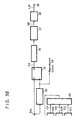
- Figure 2 is a schematic illustration of oblique tracks recorded on a magnetic tape 2 in the 8-mm format.
- a pair of diametrically opposed rotary heads is used to scan respective tracks across the tape 2 which is wrapped about a tape drum with a wrap angle of about 221°. If one video field is recorded in one track, the heads are driven at the frame rate to reproduce a video frame at each complete rotation.
- the combined frequency-multiplexed FM luminance and converted chrominance components as well as the FM audio signals are recorded along an angular extent of 180° in that portion of each track identified as the video portion 2V.
- each oblique track shown in Figure 2 by the cross-hatched sections identified as the audio portion 2A.
- These audio signals are recorded as pulse code modulated (PCM) audio signals in an angular extent of about 41° and may represent the same audio information as the FM audio signals recorded in the video portion 2V (but with better quality).
- PCM pulse code modulated
- a PCM audio signal is recorded for about 41° and then the frequency-multiplexed combined video and audio signals are recorded in the remainder of the track (about 180° ).
- the quality of the PCM audio signals is far superior.
- the FM audio signals are recorded in portion 2V as part of the frequency-multiplexed combined signals in order to be compatible with typical 8-mm standards.
- the PCM audio signals are produced by quantizing left and right channel audio channels into digital signals DD having 16 bits per sample at a sampling frequency of 48 kHz or 44.1 kHz or 32 kHz (each of which sampling frequencies has been adopted as a modification of the 8-mm recording standard).
- the digitized audio signals may be encoded in an error correcting code, such as a BCH code, or may have an error correcting code added thereto, such as a parity character, ECC code or the like.
- the digitized audio signals are timebase compressed and converted in accordance with recording code conversion techniques, such as 8-to-10 conversion.
- the resultant digitized, error-corrected, compressed and converted audio signals are recorded in the audio portion 2A of each oblique track.
- the PCM audio signal recorded as aforementioned has high quality and may be reproduced with characteristics equal to or better than the characteristics of audio signals reproduced by typical CD or R-DAT formats.
- equalizing circuitry When reproducing digital signals, such as the PCM audio signals reproduced from the tape 2 shown in Figure 2, the use of equalizing circuitry is important to the elimination of intercode interference and to permit the demodulation of the left-channel and right-channel audio signals with minimal error rate.
- proper equalization generally is dependent upon an accurate prediction of the transmission characteristics exhibited by the signal transmission system formed of the record medium, the playback head, the conducting leads and the signal processing circuitry.
- these transmission characteristics vary from one playback device (or 8-mm recorder) to another. Since the transmission characteristics depend to a significant degree upon the particular magnetic tape that is used, the availability of a wide variety of tape practically assures different transmission characteristics each time a different tape is used.
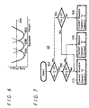
- the most favourable equalizing characteristics generally are obtained from an automatic equalizer circuit by executing a sequential executing process to arrive at the most favourable error rate.
- This sequential process is graphically depicted in Figure 4 wherein different equalizing characteristics are selected in sequence, while sensing the error rate resulting from each selected characteristic. Once this sequence has been performed, the equalizing characteristic which resulted in the most favourable error rate is selected.
- this sequential process is time-consuming, and it may take several seconds until the most favourable equalizing characteristic is selected.
- apparatus for reproducing a digital signal from a record medium comprising: playback means for playing back a digital signal from said record medium; a plurality of processing means supplied with the played back digital signal for processing said digital signal, each processing means exhibiting respective characteristics to impart a different error rate to the digital signal processed thereby; detecting means coupled to said processing means for detecting the processed digital signal having a most favourable error rate; and selecting means coupled to said processing means for selecting the processing means which produces the processed digital signal having the most favourable error rate.
- Embodiments of the invention can provide digital signal reproducing apparatus wherein a digital signal is supplied over playback apparatus that may exhibit different transmission characteristics, and wherein processing circuitry having selectable characteristics is selected quickly to minimize the error rate of the reproduced signal notwithstanding such different transmission characteristics.
- apparatus provided for reproducing a digital signal from a record medium includes a plurality of processing circuits supplied with the digital signal played back from the record medium, each processing circuit exhibiting respectively different characteristics to impart different error rates to the digital signal processed thereby.
- the processed digital signal having the most favourable error rate is detected, and the particular processing circuit which produces that digital signal is selected.
- the processing circuits may comprise equalizing circuits, waveshaping circuits or synchronizing circuits, each exhibiting slightly different characteristics from the others, thus resulting in slightly different error rates, depending upon which processing circuit is selected.
- embodiments of the invention are used to reproduce PCM audio signals from magnetic tape, such as PCM audio signals that are recorded in oblique tracks along with video signals, as are recorded in the 8-mm recording format.
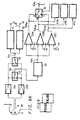
- a pair of diametrically opposed rotary magnetic heads 1A and 1B preferably mounted on a rotary head drum about which the magnetic tape 2 is deployed with a wrap angle of about 221° and having successive, parallel oblique tracks recorded thereon in the format shown in Figure 2, are rotated to scan successive tracks and thereby recover a video field from each track.
- the head 1A first scans the portion 2A of a track to reproduce PCM audio signals therefrom and then scans the portion 2B to reproduce the combined frequency multiplexed video, audio and pilot signals.
- the head 1A rotates towards the end of a track, the head 1B comes into contact with the beginning of the adjacent track so as to reproduce PCM audio signals from the portion 2A of that adjacent track. It is appreciated that the heads 1A and 1B are in simultaneous contact with the tape 2 for an angular extent of 41°, during which time one of them scans the video portion SV of one track while the other scans the audio portion SA of the next adjacent track.
- the heads 1A and 1B are coupled to playback amplifiers 11A and 11B, respectively, and the combination of the tape 2, the heads 1A and 1B, conductor leads and amplifiers comprises a playback channel.
- the amplified reproduced video signals produced by the amplifiers 11A and 11B are coupled to change-over switches 12 and 21 by which the signals reproduced by one or the other of these channels is supplied therethrough to further circuitry.
- the switch 12 may be referred to as a video selector switch for coupling the frequency-multiplexed combined video, audio and pilot signals reproduced from the video portion SV of an oblique track to a video playback processor circuit 13 and to an audio playback processor circuit 15.
- the video selector switch 12 couples the signal reproduced by the head 1A from the portion 2V to the processor circuits 13 and 15.
- the FM combined video, audio and pilot signals reproduced from the portion 2V of an oblique track are referred to simply as the video signal.
- the video selector switch 12 is changed over to couple to the processor circuits 13 and 15 the video signal reproduced by the head 1B from the portion 2V of an adjacent track when the head 1A reaches the end of the preceding track and the head 1B reaches the beginning of the video portion in the succeeding track.
- the video selector switch 12 operates to supply to the video and audio playback processor circuits 13 and 15 the FM combined video and audio signals that are reproduced from the video portion 2V of each track.
- the video playback processor circuit 13 forms no part of the present invention per se and may be of known construction to separate the FM combined video signals from the FM audio signals and to derive from the FM luminance and chrominance components standard television signals suitable for display, such as NTSC video signals.
- the audio playback processor circuit 15 forms no part of the present invention per se and may be of known construction to recover from the FM sum and difference stereophonic audio signals the left-channel and right-channel signals suitable for sound reproduction.
- the video playback processor circuit 13 is provided with an output terminal 14 to which the recovered colour composite video signal is supplied. This output video signal may be further processed, displayed or otherwise utilized by additional circuitry connected to the output terminal 14.
- the audio playback processor circuit 15 includes an output terminal, or terminals 16 to which the recovered left-channel and right-channel audio signals L, R are supplied. Additional circuitry or sound recovery apparatus may be coupled to output terminal 16 for further processing or transducing of the audio signals.
- the change-over switch 21 is referred to as an audio selector switch and is operable to select a PCM audio signal reproduced from the tape 2 by the head 1A or 1B. From Figure 2, it is seen that when one head scans the audio portion 2A of a track, the other head is in the process of scanning the video portion of the preceding track. Thus, it is a relatively simple matter to operate the audio selector switch 21 to couple the PCM audio signals alternately from the head 1A and then from the head 1B as the heads rotate.
- the output of the audio selector switch 21 is coupled in common to a plurality of digital signal processing circuits, here illustrated as three equalizer circuits 22A, 22B and 22C which may be typical playback equalizers to equalize the digital signals (the PCM audio signals) supplied thereto from the head 1A or the head 1B.
- the equalizer circuits are not of identical configuration. Rather, the operating characteristics, such as the transfer characteristics thereof, are deliberately varied from one equalizer circuit to the other.
- the playback equalizer circuit 22A may exhibit an equalization function corresponding to that shown as point 1
- the playback equalizer circuit 22B may exhibit an equalization function corresponding to point 2
- for a still further tape and head combination equalizer circuit 22C may exhibit the equalization function corresponding to point 3.
- one of the equalizer circuits will provide optimum (or at least most favourable) equalization to the digital signal reproduced from the head.
- Figure 6 is a graphical representation of the equalizer characteristics exhibited by the respective equalizer circuits.
- the equalizer circuit 22A exhibits equalizer characteristic EQA
- the equalizer circuit 22B exhibits equalizer characteristic EQB
- the equalizer circuit 22C exhibits equalizer characteristic EQC.
- Figure 6 also depicts the error rate as a function of each equalizer characteristic. Hence, for a given combination of tape and head, that is, for a given transmission function in the digital signal playback channel, each equalizer circuit imparts a different error rate to the digital signal which is equalized thereby.
- a threshold or maximum acceptable error rate
- Rth the threshold level Rth
- the equalized digital signals produced by the equalizer circuits 22A, 22B and 22C are supplied to waveform shaping circuits 23A, 23B and 23C, respectively, as equalized digital signals SA1.
- the waveform shaping circuits 23A, 23B and 23C which also are included in the digital signal processing circuitry, operate as pulse detectors and sense whether the equalized digital signal exceeds or is less than a threshold level so as to produce a "1" or "0", respectively. It will be appreciated that, depending upon the equalizer characteristics exhibited by the respective equalizer circuits and, thus, the respective error rates imparted by these equalizer circuits to the reproduced digital signal, one waveform shaping circuit may produce a "1" while the others produce a "0". That is, the waveform of the equalized digital signal may be somewhat degraded as a function of the particular equalizer characteristics exhibited by the equalizer circuits.
- the waveshaped signal SA 2A , SA 2B and SA 2C produced by the waveform shaping circuits 23A, 23B and 23C are coupled to terminals A, B and C, respectively, of a selector switch 24.
- the selector switch 24 is controlled in a manner described below such that the waveshaped digital signal having the most favourable error rate is selected and coupled as the digital signal SA3 to further circuitry.
- This further circuitry functions to demodulate the digital signal and, in the embodiment wherein the digital signal comprises a PCM audio signal, the audio information is recovered and converted to analogue form.
- Such demodulating circuitry is illustrated in Figure 5B as including a D-type flip-flop circuit 25, a demodulator 26, a playback processor 27 and a digital-to-analogue (D/A) converter 28.
- the digital signal SA3 selected by the switch 24 is supplied to the data input (the D input) of the flip-flop circuit 25, and also is coupled to a clock reproducing circuit 30.
- the clock reproducing circuit 30 is standard and functions to recover timing information included in the digital signal. As a result, a clock signal recovered from the reproduced digital signal is produced and this recovered clock signal is applied to the clock input of the flip-flop circuit 25. Consequently, the n output of the flip-flop circuit 25 produces a synchronized, or timed digital signal SA4.
- the demodulator 26 receives the synchronized digital signal SA4 and performs a 10-to-8 conversion or other conversion which is complementary to the conversion used to record the digital signal.
- the demodulator 26 thus supplies a demodulated PCM audio signal to the playback processor 27 which performs an error correction function to correct errors that may be introduced into the PCM audio signal during the recording and/or reproducing operations.
- the playback processor 27 also expands the timebase of the error-corrected PCM audio signal so as to compensate for the timebase compression that was carried out during recording.
- the original digital signal DD that is, the original PCM audio signal
- This PCM audio signal is converted to analogue form by the D/A converter 28; and the resultant left-channel and right-channel audio signals are provided at an output terminal (or terminals) 29 for further use.
- Syndrome generators 41A, 41B and 41C are coupled to the waveform shaping circuits 23A, 23B and 23C to receive waveshaped digital signals SA 2A , SA 2B and SA 2C , respectively.
- a syndrome generator may be of the type described in Information Theory and Reliable Communication , Robert G Gallagher, John Wiley & Sons, Inc, pages 200-201 and 238-259, or in Error-Correcting Codes , by Peterson and Welden, MIT Press (1981), pages 283- 307.
- each syndrome generator detects errors that may be present in the digital signals supplied thereto, these errors being detected as a function of the error correcting codes which may be used to encode the digital signal, the parity codes used with the digital signal or with the error correcting codes that may be added during recording for error detection/correction purposes.
- a particular example of a syndrome generator which may be used is shown in Figure 6.7.5 at page 255 of the Gallagher text.
- the syndrome generator produces a binary "0" output signal when no error is detected and produces an error flag when an error in the supplied digital signal is sensed.
- the syndrome generator may produce a digital output signal having a value corresponding to the number of errors which are detected.
- Error indicating signals EA, EB and EC are produced by the syndrome generators 41A, 41B and 41C, respectively, and these error indicating signals are supplied to a controller 42 which senses the error signal having the smallest value. Depending upon which error indicating switch has the lowest value, the controller 42 operates switch 24 to select the equalized, waveshaped digital signal which has that error rate.
- the audio portion 2A on each track may comprise, for example, 110 data clocks.
- Each block comprises an error correcting code and, if desired, a parity code such that an error that may be present in an individual block is readily detected.
- the syndrome generators 41A, 41B and 41C function to sense whether an error is present in a respective block of the digital signals Sa 2A , SA 2B and SA 2C supplied thereto. That is, the syndrome generators operate 41A, 41B and 41C on a block-by-block basis. Whichever block exhibits the least error rate, as sensed by the syndrome generators 41A, 41B and 41C, the controller 42 sets the switch 24 to select that block as the digital signal SA3 to be demodulated.
- a syndrome generator When operating on a block-by-block basis, a syndrome generator simply may produce an error flag when an error is detected; and the controller 42 may change the setting of the switch 24 if the present setting thereof is coupled to a data block which produces an error flag and another data block is present which does not.
- each syndrome generator 41A, 41B and 41C may operate on a block-by-block basis, thus producing an error indication (either "0" or "1") for each block.
- the controller 42 counts the number of error indications produced by each syndrome generator when the PCM audio signal is reproduced from the audio portion 2A of a track.
- each block may be stored, and the controller 42 reads out all of the stored blocks produced by the playback equalizer and waveform shaping circuits which exhibit the least number of error indications.
- the controller 42 operates the switch 24 to read out from a memory the stored blocks produced by the equalizer circuit 22B and the waveform shaping circuit 23B.
- the controller 42 operates the switch 24 to read out from a memory the data blocks processed by the equalizer 22A and the waveform shaping circuit 23A.
- the playback equalizer circuits 22A, 22B and 22C exhibit different equalizing characteristics, it is expected that different error rates will be imparted thereby to the digital signals SA 1A , SA 1B and SA 1C ; and these error rates are sensed by the syndrome generators 41A, 41B and 41C to produce error indications EA, EB and EC, respectively.
- the controller 42 determines which of these error indications is the most favourable (which error rate is the least), and operates the switch 24 to select the processed digital signal SA 2A , SA 2B , SA 2C having the most favourable error rate.
- the determination by the controller 42 as to which processed digital exhibits the most favourable error rate may be carried out on a block-by-block basis, with the setting of the switch 24 being changed at each block, or may be carried out after all of the digital signals recorded in the audio portion 2A of an oblique track have been reproduced, in which case the controller 42 may change the setting of the switch 24 as each track is scanned.
- the controller 42 may change the setting of the switch 24 as each track is scanned.
- the data blocks processed by each processing channel should be stored and then read out after all of those data blocks have been recovered from the track.
- the controller 42 may include a processor for sensing the most favourable error rate detected by the syndrome generators 41A, 41B and 41C and for coupling the switch 24 to the one input terminal A, B or C to which digital signals having the most favourable error rate are applied.
- the controller 42 compares the error indication EA produced by the syndrome generator 41A to error indication EB produced by the syndrome generator 41B.
- Inquiry 102 determines if EA > EB and, if not, a comparison between the error indication EA produced by the syndrome generator 41A to the error indication EC produced by the syndrome generator 41C is made.
- Inquiry 104 determines if EA > EC.
- the controller 42 once again advances to inquiry 104.
- inquiry 104 is answered in the affirmative, concluding that error indication EC is of the lowest value.
- the controller 42 advances to instruction 112 which sets the switch 24 to input terminal C to select the processed digital signal SA 2C (which has been detected as having the most favourable error rate) for demodulation.
- inquiry 102 is answered in the affirmative; and the controller 42 advances to inquiry 106. If error indication EB is not greater than error indication EC, inquiry 106 is answered in the negative and the controller 42 advances to instruction 110 which sets the switch 24 to the input terminal B.
- the processed digital signal SA 2B which is sensed as having the most favourable error rate, which is coupled to the demodulating circuitry.
- FIG. 5A and 5B different equalizer characteristics are provided for the purpose of matching differing transmission characteristics in a playback channel, as may be attributed to various tape-head combinations as well as the conducting leads used to couple the reproduced digital signals to the equalizers.
- Figure 6 graphically illustrates the wide equalizer margin produced by the equalizer circuits 22A, 22B and 22C. Nevertheless, it is expected that, for a given head-tape-conductor combination, the error rate imparted to one of the digital signals processed by the equalizer circuits 22A, 22B and 22C will be the lowest.
- the combination of the syndrome generators and controller functions to detect which of the processed digital signals has the lowest error rate; and the switch 24 is controlled to select that processed digital signal for demodulation.
- controller 42 may be relatively simple and, thus, inexpensive. It is expected that the cost of implementing the embodiment shown in Figure 5A is less than the cost of constructing a suitable automatic equalizer. Furthermore, and advantageously, the time needed to select the processed digital signal having the most favourable error rate is substantially less than the time needed for an automaticequalizer to undergo the sequential processing graphically depicted in Figure 4. Hence, the selection of an equalizer having the most favourable characteristics can be done almost immediately after a user first operates an 8-mm recorder to carry out a playback operation.
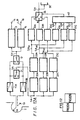
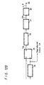
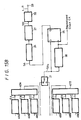
- FIG. 8A and 8B Another embodiment for implementing the present invention is illustrated in the block diagram of Figures 8A and 8B.
- a comparison of the embodiment shown in Figures 8A and 8B with the embodiment shown in Figures 5A and 5B indicates a difference in the processing circuitry that is used to process the digital signal SA recovered from the tape 2.
- a single playback equalizer circuit 22 is used, and this single equalizer circuit 22 is coupled to the waveform shaping circuits 23A, 23B and 23C illustrated as level comparators supplied with respective reference levels Va, Vb and Vc.
- Va > Vb > Vc it is expected that the equalized digital signal SA1 produced by the equalizer circuit 22 will cross reference level Vc before it crosses the reference level Vb which, in turn, will be crossed before the reference level Va.
- one of the level comparators will produce a digital signal having a more favourable error rate than the others.
- the syndrome generators 41A, 41B and 41C detect errors in the processed digital signals SA 5A , SA 5B and SA 5C produced by the waveform shaping circuits 23A, 23B and 23C, respectively, and the controller 42 senses the most favourable error rate of these processed digital signals.
- the switch 24 then is set to select for demodulation the processed digital signal having the most favourable error rate.
- Figure 9D illustrates the waveshaped digital signal SA 5C produced when the waveform SA1 exceeds the reference level Vc.
- the syndrome generator 41A detects errors in the waveshaped digital signal SA 5A
- the syndrome generator 41B detects errors in the waveshaped signal SA 5B
- the syndrome generator 41C detects errors in the waveshaped signal SA 5C .
- the controller 42 operates the switch 24 to couple the input terminal B to the demodulating circuitry, whereupon the waveshaped digital signal SA 5B shown in Figure 9C, having the most favourable error rate, is demodulated.
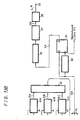
- FIG. 10A and 10B Yet another embodiment of the present invention is illustrated in Figures 10A and 10B.
- the processing circuitry that is used to process the reproduced digital signal SA in this embodiment is modified relative to that of Figures 5A and 5B.
- the reproduced digital signal is equalized and waveshaped; but in the present embodiment, a single equalizer circuit 22 and a single waveform shaping circuit 23 are used to produce the equalized, shaped digital signal SA2.
- the equalized, shaped digital signal SA2 is coupled to a synchronizing circuit for synchronizing the reproduced digital signal with clock signals of respectively different phases.
- the synchronizing circuit shown in the embodiment of Figure 5 comprises a D-type flip-flop circuit 25 and a clock recovery circuit 30.
- a similar synchronizing circuit is provided, wherein a plurality of D-type flip-flop circuits 25A, 25B and 25C have their D inputs connected in common to receive the reproduced digital signal SA2.
- a clock reproducing circuit 30, which may include a phase locked loop, also receives the reproduced digital signal SA2 and operates to recover a clock signal CKA therefrom.
- the recording format used to record the digital signal may be such that the recorded digital signal is a self-clocking signal; and this self-clocking feature is standard and used by reproducing circuit 30 to recover the clock signal CKA.
- the clock signal CKA is coupled to the timing input of the D-type flip-flop circuit 25A, and is also supplied through a delay, or phase shift circuit 31B to the timing input of the flip-flop circuit 25B as the clock signal CKB.
- the clock signal CKB is also coupled through a delay or phase shift circuit 31C to the timing input of the flip-flop circuit 25C as the clock signal CKC.
- the clock signals CKA, CKB and CKC exhibit a relative time shift with respect to each other, for example, a shift of about 120°.
- the reproduced digital signal SA2 is synchronized with successively shifted clock signals CKA, CKB and CKC by the flip-flop circuits 25A, 25B and 25C, respectively.
- a relatively narrow pulse included in the reproduced digital signal SA2 may be synchronized with one clock signal, such as the clock signal CKA, to produce a synchronized with "1", but another clock signal, such as the clock signal CKC, may occur after this narrow pulse terminates such that another flip-flop circuit, such as the flip-flop circuit 25C, produces a "0".
- the synchronized digital signals SA 8A , SA 8B and SA 8C produced by the flip-flop circuits 25A, 25B and 25C, respectively, are supplied to the syndrome generators 41A, 41B and 41C, respectively, for the detection of errors therein.
- the controller 42 senses the most favourable error rate in response to the error indications EA, EB and EC produced by these syndrome generators so as to set the switch 24 to the input terminal to which the synchronized digital signal having the most favourable error rate is applied.
- the clock signals CKA, CKB and CKC which are time (or phase) shifted with respect to each other also are supplied to input terminals A, B and C, respectively, of a clock selector switch 34.
- the clock selector switch 34 is controlled by the controller 42 to select the particular clock signal that is used to synchronize the reproduced digital signal having the most favourable error rate.
- the clock signal to which the reproduced digital signal is synchronized is recovered and may be used by other circuitry (not shown).
- Figure 11C illustrates the reproduced clock signal CKA recovered from the digital signal SA2 by the clock reproducing circuit 30.
- the delay circuit 31B delays the clock signal CKA by a predetermined amount to produce the clock signal CKB illustrated in Figure 11D.
- the delay circuit 31C delays the clock signal CKB by a similar predetermined amount to produce the clock signal CKC shown in Figure 11E.
- each D-type flip-flop circuit 25A, 25B and 25C responds to the positive transition of the clock signals supplied thereto, it is seen that the flip-flop circuit 25A responds to the positive transitions of the clock signal CKA to produce the following output signal SA 8A : the transition tA1 produces a "1”, the transition tA2 produces a "0”, the transition tA3 produces a “1”, and the transition tA4 produces a "0".
- the flip-flop circuit 25B responds to the positive transitions of the clock signal CKB to produce the following digital signal SA 8B : the transition tB1, produces a "1", the transition tB2 produces a "0”, the transition tB3 produces a “1”, and the transition tB4 produces a "1".
- the flip-flop circuit 25C responds to the positive transitions of the clock signal CKC to produce digital signal SA 8C as follows: the transition tC1 produces a "0”, the transition tC2 produces a “0”, the transition tC3 produces a “0”, and the transition tC4 produces a "1".
- the synchronized digital signal SA 8A accurately reproduces, in timed relationship, the equalized, waveshaped digital signal SA2.
- the synchronized digital signals SA 8B and SA 8C exhibit errors therein due to the phase shift of the clock signals supplied to the flip-flop circuits 25B and 25C.
- the syndrome generator 41A produces an error indication EA whose value is less than error indications EB and EC produced by the syndrome generators 41B and 41C.
- the controller 42 sets the switch 24 to couple the input terminal A to the demodulating circuitry, thereby supplying the synchronized digital signal SA 8A from the flip-flop circuit 25A to the demodulator 26. That is, the synchronized digital signal having the most favourable error rate is selected for demodulation.
- the controller 42 Since the synchronized digital signal which is selected for demodulation is synchronized to the clock signal CKA, the controller 42 sets the clock generator switch 34 to its input terminal A to couple the clock signals CKA (to which the synchronized digital signal is synchronized) to further circuitry for use as may be needed.
- FIG. 12A and 12B there is illustrated a modification of the embodiment shown in Figures 5A and 5B in which the equalized, waveshaped digital signals SA 2A , SA 2B and SA 2C are supplied to the input terminals A, B and C of the selector switch 24 by way of memory devices 33A, 33B and 33C, respectively.
- These memory devices 33A, 33B and 33C may be the memories discussed above in conjunction with the Figure 5 embodiment, wherein blocks of PCM audio signals included in, for example, the audio portion 2A of a track are stored until the controller 42 determines which of these stored digital signals exhibits the most favourable error rate.
- the memory devices 33A, 33B and 33C function to store a block of the equalized, waveshaped digital signals SA 2A , SA 2B and SA 2C , respectively, until the controller 42 determines which of these blocks exhibits the most favourable error rate.
- the block or blocks stored in a memory device is read therefrom in synchronism with the output signal produced by the controller 42.
- the switch 24 may be implemented by supplying a read enable signal from the controller 42 to the particular memory device in which is stored the block (or blocks) having the most favourable error rate.
- FIG. 13A and 13B A still further embodiment of the present invention is illustrated in Figures 13A and 13B.
- This embodiment is seen to be quite similar to that shown in Figure 5, with the following additional feature: the energizing power supplied to each processing circuit (to the cascaded equalizer and waveshaping circuits) is selectively interrupted by a switch controlled by the controller 42.
- a suitable power supply schematically represented as power supply 49
- the switch 44A also couples energizing power to the syndrome generator 41A.
- a switch 44B couples the power supply 49 to the equalizer circuit 22B, the waveform shaping circuit 23B and the syndrome generator 41B.
- a switch 44C couples the power supply 49 to the equalizer circuit 22C, the waveform shaping circuit 23C and the syndrome generator 41C.
- the purpose of the switches 44A, 44B and 44C is to minimize power consumption by those processing circuits which are not selected for processing the reproduced digital signal because they do not exhibit the most favourable error rate.
- the controller 42 periodically closes all of the switches 44A, 44B and 44C for a predetermined duration sufficient for the equalizer circuits, waveform shaping circuits and syndrome generators to operate and supply error indications EA, EB and EC to the controller 42.
- the controller 42 determines which of the processing circuits produces an equalized, waveshaped digital signal SA2 of lowest error rate, the switch which couples energizing power to that processing circuit is maintained closed and the other two switches are opened.
- the processing circuit which produces the digital signal SA2 with the most favourable error rate is energized.
- the remaining processing circuits whose output digital signals are not supplied to the demodulating circuitry are deenergized, thereby conserving power.
- the foregoing operation is repeated periodically by the controller 42 so as to update the determination and selection of the processed digital signal having the most favourable error rate.
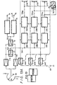
- FIG. 14A and 14B Yet another embodiment of the present invention is illustrated in Figures 14A and 14B.
- the processing circuitry used to process the digital signal SA reproduced from the tape 2 is implemented by respective processors 50A, 50B and 50C, each arranged to execute a respective algorithm which functions to equalize, waveshape and synchronize the reproduced digital signal.
- Each algorithm differs somewhat from the others, and may be thought of as being matched to the expected transmission characteristics of a particular playback channel. Since these transmission characteristics may differ from device to device, and particularly when tape of different quality and recording characteristics is used, the effect of using processors 50A, 50B and 50C is analogous to that of using different equalizer and waveshaping circuits.
- the syndrome generators 41A, 41B and 41C produce error indications EA to EC representing such error rates; and the controller 42 senses the error signal having the lowest value.
- the switch 24 is set to couple the processed digital signal exhibiting the most favourable error rate to the demodulating circuitry.
- the embodiments shown in Figures 14A and 14B also include power supply switches 44A, 44B and 44C, similar to the power supply switches discussed about in conjunction with Figures 13A and 13B.
- the controller 42 maintains closed the energizing switch which supplies energizing power to the processor that produces the processed digital signal having the most favourable error rate. The remaining power supply switches are opened so as to conserve power.
- the controller 42 operates to close all of the power supply switches periodically and then, after the most favourable error rate is sensed, the controller 42 opens those power supply switches that supply energizing power to the processing circuits that do not produce the digital signal having that error rate.
- the power supply switches 44A, 44B and 44C minimize power consumption.
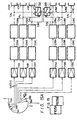
- Figures 15A and 15B A still further embodiment of the present invention is illustrated in Figures 15A and 15B. It will be seen that this embodiment is somewhat similar to the embodiment discussed above in conjunction with Figure 5, with the following noted changes.
- the Figure 5 embodiment includes a pair of diametrically opposed heads 1A and 1B
- the embodiment shown in Figure 15A includes a pair of diametrically opposed head assemblies, with each assembly including a plurality of heads, such as three heads.
- assembly A includes heads 1AA, 1AB, 1AC
- assembly B includes 1BA, 1BB and 1BC.
- the heads in a respective assembly are slightly offset from each other so that a single track is scanned simultaneously by the three heads, with the position of each head along the scanned track being displaced along the width of the track.
- the three heads reproduce digital signals having different characteristics because of the relative position of each head with respect to the track.
- the circuitry used to reproduce the signals recovered from video portion SV of each track comprises the playback amplifiers 11, the playback equalizer circuits 22, the waveform shaping circuits 23, the syndrome generators 41, the controllers 42, and the selector switches 24, disposed in separate, but substantially identical, channels A and B.
- Each of the heads 1AA, 1AB and 1AC is coupled to a respective playback channel including playback amplifiers 11AA, 11AB and 11AC, respectively.
- These playback amplifiers are coupled to the equalizer circuits 22AA, 22AB and 22AC which, in turn, are coupled to the waveform shaping circuits 23AA, 23AB, 23AC, respectively. It is appreciated that, because of the particular characteristics of the signals reproduced by the heads 1AA, 1AB and 1AC, combined with the equalizing characteristics of the equalizer circuits 22AA, 22AB and 22AC, as well as the operating characteristics of the waveform shaping circuits 23AA, 23AB and 23AC, the processed digital signals SA2 produced by each of these playback channels exhibit respectively different error rates.
- the processed digital signals SA2 are supplied to the syndrome generators 41AA, 41AB and 41AC which, as discussed above, produce the error indications EA, EB and EC.
- a controller 42 senses the error indication having the lowest value and, thus, determines which of the processed digital signals SA2 in channel A exhibits the most favourable rate.
- the selector switch 24A is controlled by the controller 42A to select the processed digital signal having the most favourable error rate.
- the processed digital signal selected by the switch 24A is coupled to the change-over switch 21, which is similar to the change-over switch 21 shown in Figure 5.
- the change-over switch 21 in combination with the selector switch 24A supplies to the demodulating circuitry the processed digital signal SA2 in channel A having the most favourable error rate.
- the heads 1BA, 1BB and 1BC are coupled to playback amplifiers 11BA, 11BB and 11BC which, in turn, are coupled to playback equalizer circuits 22BA, 22BB and 22BC in respective playback channels.
- These equalizer circuits are coupled to waveform shaping circuits 23BA, 23BB and 23BC to produce the processed digital signals SA2 in channel B which are supplied to syndrome generators 41BA, 41BB and 41BC.
- syndrome generators are similar to the aforementioned syndrome generators 41AA, 41AB and 41AC and produce the error indications EA, EB and EC which are supplied to a controller 42B.
- the digital signal processing circuitry coupled to the heads 1BA, 1BB and 1BC in channel B is similar to and functions in a manner substantially the same as that of the aforedescribed processing circuitry coupled to the heads 1AA, 1AB and 1AC in channel A.
- the digital signals SA2 produced by the waveform shaping circuits 23BA, 23BB and 23BC exhibit respectively different error rates. These different error rates are detected by the syndrome generators 41BA, 41BB and 41BC which produce error indications EA to EC.
- the controller 42B senses the error indication having the least value and sets a switch 24B to couple the processed digital signal having the most favourable error rate produced by the waveform shaping circuits 23BA, 23BB and 23BC.
- This processed digital signal is supplied by the change-over switch 21 to the demodulating circuitry when the heads 1BA, 1BB and 1BC scan the audio portion 2A of a record track.
- processing circuitry used to produce the processed digital signals SA2 is shown in Figure 15A as comprising individual channels of cascaded equalizer and waveform shaping circuits connected to receive a digital signal reproduced by a respective one of the plurality of heads included in each head assembly, it will be appreciated that other embodiments of the processing circuitry may be used, such as those embodiments shown and prescribed hereinabove in conjunction with the block diagrams of Figures 5, 8, 10, 12, 13 and 14.
- the plurality of playback heads in each head assembly define a plurality of playback channels, each having a respective processing circuit included therein, and the one processing circuit which provides the digital signal having the most favourable error rate is selected to couple that digital signal to demodulating circuitry.
- Figures 15A and 15B illustrate the selector switch 21 as being coupled to receive the processed digital signals selected either by the switch 24A or 24B
- this embodiment may be modified to provide a plurality of channels of processing circuits for common use by the digital signals reproduced by the head assembly A or by the head assembly B.
- the selector switch 21 may be provided with two sets of input terminals and one set of output terminals, with the two sets of input terminals being connected to playback amplifiers 11AA, 11AB and 11AC and to the playback amplifiers 11BA, 11BB and 11BC, respectively, and the one set of output terminals being connected to the equalizer circuits 22AA, 22AB and 22AC.
- the equalizer circuits 22BA, 22BB and 22BC, the waveform shaping circuits 23BA, 23BB and 23BC, the switch 24B, the syndrome generators 41BA, 41BB and 41BC, and the controller 42B may be omitted.
- the present invention admits of wider application and need not be used solely to recover PCM audio signals recorded on an 8-mm video recording tape. More generally, digital signals representing virtually any type of information may be recovered from magnetic media, such as magnetic tape, discs, sheets, stripes, etc, or from other media, such as optical discs or other optical recording media. Also, various combinations of processing circuitry components may be used to implement the digital signal processing circuit that is used to produce the digital signal SA2 that is selected for demodulation.
Abstract

Description
- This invention relates to digital signal reproducing apparatus.
- In the field of video signal recording, a so-called 8-mm recording format has become popular. In 8-mm recording, both video and audio signals are recorded in oblique tracks by rotary heads, with one field of video signals recorded in each track. Consistent with a standard which has developed, video and audio signals are frequency multiplexed for recording in a common track.
- A typical frequency spectrum used with 8-mm recording is illustrated in Figure 1. As shown, the frequency multiplexed signals comprise the combination of a frequency modulated (FM) luminance signal SF, a frequency-converted chrominance signal SC, FM audio signals SM and SS, and pilot signals SP. The FM luminance signal is formed of a carrier which is frequency modulated with the luminance component SY such that the frequency representing the sync tip level is about 5.7 MHz and the frequency which represents the white peak level of the luminance component is about 7.7 MHz.
- The frequency-converted chrominance signal is formed by frequency-converting the chrominance sub-carrier to a relatively low range below that of the FM luminance component. The technique of providing an FM luminance component and a frequency-converted chrominance component is well known.
- The FM audio signal SM comprises a carrier that is frequency modulated with the sum (L + R) of the left-channel and right-channel stereophonic audio signals; and the FM audio signal SS comprises another carrier that is frequency modulated with the difference (L - R) between the left-channel and right-channel stereophonic signals. It is appreciated that, on reproduction, good stereophonic quality can be recovered from the FM audio signals SM and SS that have been recorded in an oblique track.
- The pilot signals SP are used for tracking servo control when the frequency-multiplexed combined signals are reproduced. As is usual in 8-mm recording, a respective pilot signal whose frequency is one of four different pilot frequencies is recorded in each track such that when a playback head picks up a pilot signal from an adjacent track, the magnitude of that picked up signal is indicative of the tracking error of the head and the frequency of that signal represents the direction in which the head has drifted from its desired position. Thus, tracking control is attained as a function of pilot signal cross-talk components which are picked up when a given track is scanned.
- Figure 2 is a schematic illustration of oblique tracks recorded on a
magnetic tape 2 in the 8-mm format. Typically, a pair of diametrically opposed rotary heads is used to scan respective tracks across thetape 2 which is wrapped about a tape drum with a wrap angle of about 221°. If one video field is recorded in one track, the heads are driven at the frame rate to reproduce a video frame at each complete rotation. The combined frequency-multiplexed FM luminance and converted chrominance components as well as the FM audio signals are recorded along an angular extent of 180° in that portion of each track identified as thevideo portion 2V. To improve the audio quality of 8-mm recording, it is optional also to record audio signals in a separate portion of each oblique track shown in Figure 2 by the cross-hatched sections identified as the audio portion 2A. These audio signals are recorded as pulse code modulated (PCM) audio signals in an angular extent of about 41° and may represent the same audio information as the FM audio signals recorded in thevideo portion 2V (but with better quality). Thus, to record the oblique tracks illustrated in Figure 2, a PCM audio signal is recorded for about 41° and then the frequency-multiplexed combined video and audio signals are recorded in the remainder of the track (about 180° ). Even if the very same audio signals are recorded as both FM audio signals SM and SS and as PCM audio signals, the quality of the PCM audio signals is far superior. Nevertheless, the FM audio signals are recorded inportion 2V as part of the frequency-multiplexed combined signals in order to be compatible with typical 8-mm standards. - Typically, the PCM audio signals are produced by quantizing left and right channel audio channels into digital signals DD having 16 bits per sample at a sampling frequency of 48 kHz or 44.1 kHz or 32 kHz (each of which sampling frequencies has been adopted as a modification of the 8-mm recording standard). The digitized audio signals may be encoded in an error correcting code, such as a BCH code, or may have an error correcting code added thereto, such as a parity character, ECC code or the like. Then, the digitized audio signals are timebase compressed and converted in accordance with recording code conversion techniques, such as 8-to-10 conversion. The resultant digitized, error-corrected, compressed and converted audio signals are recorded in the audio portion 2A of each oblique track.
- The PCM audio signal recorded as aforementioned has high quality and may be reproduced with characteristics equal to or better than the characteristics of audio signals reproduced by typical CD or R-DAT formats.
- When reproducing digital signals, such as the PCM audio signals reproduced from the
tape 2 shown in Figure 2, the use of equalizing circuitry is important to the elimination of intercode interference and to permit the demodulation of the left-channel and right-channel audio signals with minimal error rate. However, proper equalization generally is dependent upon an accurate prediction of the transmission characteristics exhibited by the signal transmission system formed of the record medium, the playback head, the conducting leads and the signal processing circuitry. Usually, these transmission characteristics vary from one playback device (or 8-mm recorder) to another. Since the transmission characteristics depend to a significant degree upon the particular magnetic tape that is used, the availability of a wide variety of tape practically assures different transmission characteristics each time a different tape is used. Thus, and with reference to Figure 3, even if an equalizing circuit having an optimum equalization characteristic is selected, such as the characteristic indicated atpoint 2 for a particular tape, when other tapes are used the very same equalizing circuit may exhibit the relative equalization characteristic indicated atpoints point 2 is used, poorer (higher) error rates may result when magnetic tapes corresponding topoints - The problem of matching equalization characteristics to transmission characteristics, and particularly to the type of tape and head which are used to reproduce digital signals may be overcome by using automatic equalizing circuits. However, such automatic equalizing circuits are complex and expensive and may contribute to a significantly higher overall cost of the 8-mm recorder.
- Furthermore, the most favourable equalizing characteristics generally are obtained from an automatic equalizer circuit by executing a sequential executing process to arrive at the most favourable error rate. This sequential process is graphically depicted in Figure 4 wherein different equalizing characteristics are selected in sequence, while sensing the error rate resulting from each selected characteristic. Once this sequence has been performed, the equalizing characteristic which resulted in the most favourable error rate is selected. However, this sequential process is time-consuming, and it may take several seconds until the most favourable equalizing characteristic is selected. Thus, there is a substantial and undesired time delay from the time a user first operates an 8-mm recorder to carry out a playback operation until satisfactory audio quality is obtained.
- According to the present invention there is provided apparatus for reproducing a digital signal from a record medium, the apparatus comprising:
playback means for playing back a digital signal from said record medium;
a plurality of processing means supplied with the played back digital signal for processing said digital signal, each processing means exhibiting respective characteristics to impart a different error rate to the digital signal processed thereby;
detecting means coupled to said processing means for detecting the processed digital signal having a most favourable error rate; and selecting means coupled to said processing means for selecting the processing means which produces the processed digital signal having the most favourable error rate. - Embodiments of the invention can provide digital signal reproducing apparatus wherein a digital signal is supplied over playback apparatus that may exhibit different transmission characteristics, and wherein processing circuitry having selectable characteristics is selected quickly to minimize the error rate of the reproduced signal notwithstanding such different transmission characteristics.
- In an embodiment of the invention, apparatus provided for reproducing a digital signal from a record medium includes a plurality of processing circuits supplied with the digital signal played back from the record medium, each processing circuit exhibiting respectively different characteristics to impart different error rates to the digital signal processed thereby. The processed digital signal having the most favourable error rate is detected, and the particular processing circuit which produces that digital signal is selected.
- The processing circuits may comprise equalizing circuits, waveshaping circuits or synchronizing circuits, each exhibiting slightly different characteristics from the others, thus resulting in slightly different error rates, depending upon which processing circuit is selected.
- Advantageously, embodiments of the invention are used to reproduce PCM audio signals from magnetic tape, such as PCM audio signals that are recorded in oblique tracks along with video signals, as are recorded in the 8-mm recording format.
- The invention will now be described by way of example with reference to the accompanying drawings, throughout which like parts are referred to by like references, and in which:
- Figure 1 is a graphical representation of the frequency spectrum normally used in 8-mm video recording;
- Figure 2 is a schematic representation of oblique tracks recorded in accordance with the 8-mm recording format;
- Figure 3 is a graphical representation of the relationship between equalizing characteristics and error rate for a particular playback arrangement;
- Figure 4 is a graphical representation of the sequential process used to select an automatic equalizing characteristic for a digital signal playback arrangement whose transmission characteristics are not predictable;
- Figures 5A and 5B are a block diagram representing one embodiment of the present invention;
- Figure 6 is a graphical representation of the equalizing characteristics exhibited by the arrangement shown in Figures 5A and 5B;
- Figure 7 is a flow chart which represents the manner in which the controller used in the embodiment of Figures 5A and 5B to detect the most favoured error rate;
- Figures 8A and 8B comprise a block diagram of another embodiment of the present invention;
- Figures 9A to 9D are waveform diagrams for understanding the manner in which the embodiment shown in Figures 8A and 8B operates;
- Figures 10A and 10B comprise a block diagram representing a still further embodiment of the present invention;
- Figures 11A to 11E are timing diagrams for understanding the manner in which the embodiment of Figures 10A and 10B operates;
- Figures 12A and 12B illustrate a variation of the embodiment shown in Figures 5A and 5B;
- Figures 13A and 13B illustrate another variation of the embodiment shown in Figures 5A and 5B;
- Figures 14A and 14B comprise a block diagram representing a still further embodiment of the present invention; and
- Figures 15A and 15B are a block diagram of another embodiment of the present invention;
- Although the embodiments of the present invention have more general application to the reproduction of a digital signal from a record medium, to best appreciate this invention it is described in the environment of a video signal reproducing device, and in particular, to an 8-mm recorder which operates in a playback mode to reproduce the combined frequency multiplexed video and audio signals shown in Figure 1 as well as the PCM audio signals recorded in lengths 2A of the record tracks.
- Referring to Figures 5A and 5B, a pair of diametrically opposed rotary
magnetic heads magnetic tape 2 is deployed with a wrap angle of about 221° and having successive, parallel oblique tracks recorded thereon in the format shown in Figure 2, are rotated to scan successive tracks and thereby recover a video field from each track. Assuming clockwise rotation, it is recognized that thehead 1A first scans the portion 2A of a track to reproduce PCM audio signals therefrom and then scans the portion 2B to reproduce the combined frequency multiplexed video, audio and pilot signals. As thehead 1A rotates towards the end of a track, thehead 1B comes into contact with the beginning of the adjacent track so as to reproduce PCM audio signals from the portion 2A of that adjacent track. It is appreciated that theheads tape 2 for an angular extent of 41°, during which time one of them scans the video portion SV of one track while the other scans the audio portion SA of the next adjacent track. - The
heads playback amplifiers tape 2, theheads amplifiers switches switch 12 may be referred to as a video selector switch for coupling the frequency-multiplexed combined video, audio and pilot signals reproduced from the video portion SV of an oblique track to a videoplayback processor circuit 13 and to an audioplayback processor circuit 15. With reference to Figure 2, it is seen that when thehead 1A, for example, rotates into contact with the beginning of the video portion SV of a track, thevideo selector switch 12 couples the signal reproduced by thehead 1A from theportion 2V to theprocessor circuits portion 2V of an oblique track are referred to simply as the video signal. It will be appreciated that thevideo selector switch 12 is changed over to couple to theprocessor circuits head 1B from theportion 2V of an adjacent track when thehead 1A reaches the end of the preceding track and thehead 1B reaches the beginning of the video portion in the succeeding track. Thus, thevideo selector switch 12 operates to supply to the video and audioplayback processor circuits video portion 2V of each track. - The video
playback processor circuit 13 forms no part of the present invention per se and may be of known construction to separate the FM combined video signals from the FM audio signals and to derive from the FM luminance and chrominance components standard television signals suitable for display, such as NTSC video signals. Likewise, the audioplayback processor circuit 15 forms no part of the present invention per se and may be of known construction to recover from the FM sum and difference stereophonic audio signals the left-channel and right-channel signals suitable for sound reproduction. - The video
playback processor circuit 13 is provided with anoutput terminal 14 to which the recovered colour composite video signal is supplied. This output video signal may be further processed, displayed or otherwise utilized by additional circuitry connected to theoutput terminal 14. Similarly, the audioplayback processor circuit 15 includes an output terminal, orterminals 16 to which the recovered left-channel and right-channel audio signals L, R are supplied. Additional circuitry or sound recovery apparatus may be coupled tooutput terminal 16 for further processing or transducing of the audio signals. - The change-
over switch 21 is referred to as an audio selector switch and is operable to select a PCM audio signal reproduced from thetape 2 by thehead audio selector switch 21 to couple the PCM audio signals alternately from thehead 1A and then from thehead 1B as the heads rotate. - The output of the
audio selector switch 21 is coupled in common to a plurality of digital signal processing circuits, here illustrated as threeequalizer circuits head 1A or thehead 1B. Here, however, the equalizer circuits are not of identical configuration. Rather, the operating characteristics, such as the transfer characteristics thereof, are deliberately varied from one equalizer circuit to the other. For example, and with reference to the graphical depiction shown in Figure 3, for a given magnetic tape and head, theplayback equalizer circuit 22A may exhibit an equalization function corresponding to that shown as point 1, for another tape and headcombination equalizer circuit 22B may exhibit an equalization function corresponding to point 2 and for a still further tape and headcombination equalizer circuit 22C may exhibit the equalization function corresponding topoint 3. Thus, it is expected that, for a given combination of tape, head and conductor leads, one of the equalizer circuits will provide optimum (or at least most favourable) equalization to the digital signal reproduced from the head. - Figure 6 is a graphical representation of the equalizer characteristics exhibited by the respective equalizer circuits. In the illustrated example, the
equalizer circuit 22A exhibits equalizer characteristic EQA, theequalizer circuit 22B exhibits equalizer characteristic EQB, and theequalizer circuit 22C exhibits equalizer characteristic EQC. Figure 6 also depicts the error rate as a function of each equalizer characteristic. Hence, for a given combination of tape and head, that is, for a given transmission function in the digital signal playback channel, each equalizer circuit imparts a different error rate to the digital signal which is equalized thereby. - If a threshold (or maximum acceptable error rate) is represented as the threshold level Rth, it is seen that the equalizer characteristic curves EQA and EQB, as well as the equalizer characteristic curves EQB and EQC, intersect each other at an error rate level below this threshold level.
- The equalized digital signals produced by the
equalizer circuits waveform shaping circuits waveform shaping circuits - The waveshaped signal SA2A, SA2B and SA2C produced by the
waveform shaping circuits selector switch 24. Theselector switch 24 is controlled in a manner described below such that the waveshaped digital signal having the most favourable error rate is selected and coupled as the digital signal SA₃ to further circuitry. This further circuitry functions to demodulate the digital signal and, in the embodiment wherein the digital signal comprises a PCM audio signal, the audio information is recovered and converted to analogue form. Such demodulating circuitry is illustrated in Figure 5B as including a D-type flip-flop circuit 25, ademodulator 26, aplayback processor 27 and a digital-to-analogue (D/A)converter 28. The digital signal SA₃ selected by theswitch 24 is supplied to the data input (the D input) of the flip-flop circuit 25, and also is coupled to aclock reproducing circuit 30. Theclock reproducing circuit 30 is standard and functions to recover timing information included in the digital signal. As a result, a clock signal recovered from the reproduced digital signal is produced and this recovered clock signal is applied to the clock input of the flip-flop circuit 25. Consequently, the n output of the flip-flop circuit 25 produces a synchronized, or timed digital signal SA₄. - The
demodulator 26 receives the synchronized digital signal SA₄ and performs a 10-to-8 conversion or other conversion which is complementary to the conversion used to record the digital signal. Thedemodulator 26 thus supplies a demodulated PCM audio signal to theplayback processor 27 which performs an error correction function to correct errors that may be introduced into the PCM audio signal during the recording and/or reproducing operations. Theplayback processor 27 also expands the timebase of the error-corrected PCM audio signal so as to compensate for the timebase compression that was carried out during recording. Hence, the original digital signal DD, that is, the original PCM audio signal, is recovered. This PCM audio signal is converted to analogue form by the D/A converter 28; and the resultant left-channel and right-channel audio signals are provided at an output terminal (or terminals) 29 for further use. - The apparatus used to control the
switch 24 to select the equalized, waveshaped digital signal having the most favourable error rate (for example, the digital signal exhibiting the lowest error rate) now will be described.Syndrome generators waveform shaping circuits syndrome generators controller 42 which senses the error signal having the smallest value. Depending upon which error indicating switch has the lowest value, thecontroller 42 operatesswitch 24 to select the equalized, waveshaped digital signal which has that error rate. - In the environment wherein the digital signal SA is a PCM audio signal, the audio portion 2A on each track may comprise, for example, 110 data clocks. Each block comprises an error correcting code and, if desired, a parity code such that an error that may be present in an individual block is readily detected. The
syndrome generators syndrome generators controller 42 sets theswitch 24 to select that block as the digital signal SA₃ to be demodulated. When operating on a block-by-block basis, a syndrome generator simply may produce an error flag when an error is detected; and thecontroller 42 may change the setting of theswitch 24 if the present setting thereof is coupled to a data block which produces an error flag and another data block is present which does not. - As an alternative mode of operation, each
syndrome generator controller 42 counts the number of error indications produced by each syndrome generator when the PCM audio signal is reproduced from the audio portion 2A of a track. In addition to being supplied to the respective syndrome generators on a block-by-block basis, each block may be stored, and thecontroller 42 reads out all of the stored blocks produced by the playback equalizer and waveform shaping circuits which exhibit the least number of error indications. For example, if all of the blocks recovered from the audio portion 2A by theplayback equalizer circuit 22B and thewaveform shaping circuit 23B have the least number of errors indicated by thesyndrome generator 41B, thecontroller 42 operates theswitch 24 to read out from a memory the stored blocks produced by theequalizer circuit 22B and thewaveform shaping circuit 23B. Alternatively, if the number of errors indicated by thesyndrome generator 41A for the PCM audio signal reproduced from the audio portion 2A is the least, thecontroller 42 operates theswitch 24 to read out from a memory the data blocks processed by theequalizer 22A and thewaveform shaping circuit 23A. - Thus, it is appreciated that if the
playback equalizer circuits syndrome generators controller 42 determines which of these error indications is the most favourable (which error rate is the least), and operates theswitch 24 to select the processed digital signal SA2A, SA2B, SA2C having the most favourable error rate. As mentioned above, the determination by thecontroller 42 as to which processed digital exhibits the most favourable error rate may be carried out on a block-by-block basis, with the setting of theswitch 24 being changed at each block, or may be carried out after all of the digital signals recorded in the audio portion 2A of an oblique track have been reproduced, in which case thecontroller 42 may change the setting of theswitch 24 as each track is scanned. Of course, if an error rate detection is carried out only after all of the data blocks in an audio portion 2A of a track have been reproduced, the data blocks processed by each processing channel should be stored and then read out after all of those data blocks have been recovered from the track. - The manner in which the
controller 42 operates now will be described in conjunction with the flow chart illustrated in Figure 7. As will be appreciated, thecontroller 42 may include a processor for sensing the most favourable error rate detected by thesyndrome generators switch 24 to the one input terminal A, B or C to which digital signals having the most favourable error rate are applied. Initially, thecontroller 42 compares the error indication EA produced by thesyndrome generator 41A to error indication EB produced by thesyndrome generator 41B.Inquiry 102 determines if EA > EB and, if not, a comparison between the error indication EA produced by thesyndrome generator 41A to the error indication EC produced by thesyndrome generator 41C is made.Inquiry 104 determines if EA > EC. If this inquiry is answered in the negative, it is concluded that the value of error indication EA is the lowest and processed digital signal SA2A exhibits the lowest error rate. Consequently, thecontroller 42 advances toinstruction 108 which operates theswitch 24 to select the input terminal A and thereby couple the processed digital signal SA2A to the demodulator. - Returning to
inquiry 102 and assuming once again that EA is not greater than EB, thecontroller 42 once again advances toinquiry 104. Now, if EA > EC,inquiry 104 is answered in the affirmative, concluding that error indication EC is of the lowest value. Hence, thecontroller 42 advances toinstruction 112 which sets theswitch 24 to input terminal C to select the processed digital signal SA2C (which has been detected as having the most favourable error rate) for demodulation. - Assuming that EA > EB,
inquiry 102 is answered in the affirmative; and thecontroller 42 advances toinquiry 106. If error indication EB is not greater than error indication EC,inquiry 106 is answered in the negative and thecontroller 42 advances toinstruction 110 which sets theswitch 24 to the input terminal B. Thus, the processed digital signal SA2B, which is sensed as having the most favourable error rate, which is coupled to the demodulating circuitry. - In the embodiment shown in Figures 5A and 5B, different equalizer characteristics are provided for the purpose of matching differing transmission characteristics in a playback channel, as may be attributed to various tape-head combinations as well as the conducting leads used to couple the reproduced digital signals to the equalizers. Figure 6 graphically illustrates the wide equalizer margin produced by the
equalizer circuits equalizer circuits switch 24 is controlled to select that processed digital signal for demodulation. - It will be appreciated that the
controller 42 may be relatively simple and, thus, inexpensive. It is expected that the cost of implementing the embodiment shown in Figure 5A is less than the cost of constructing a suitable automatic equalizer. Furthermore, and advantageously, the time needed to select the processed digital signal having the most favourable error rate is substantially less than the time needed for an automaticequalizer to undergo the sequential processing graphically depicted in Figure 4. Hence, the selection of an equalizer having the most favourable characteristics can be done almost immediately after a user first operates an 8-mm recorder to carry out a playback operation. - Another embodiment for implementing the present invention is illustrated in the block diagram of Figures 8A and 8B. A comparison of the embodiment shown in Figures 8A and 8B with the embodiment shown in Figures 5A and 5B indicates a difference in the processing circuitry that is used to process the digital signal SA recovered from the
tape 2. In the Figure 8 embodiment, a singleplayback equalizer circuit 22 is used, and thissingle equalizer circuit 22 is coupled to thewaveform shaping circuits equalizer circuit 22 will cross reference level Vc before it crosses the reference level Vb which, in turn, will be crossed before the reference level Va. Hence, depending upon the particular waveform produced by theequalizer circuit 22, which is a function of the tape-head-conductor characteristics of the playback channel, one of the level comparators will produce a digital signal having a more favourable error rate than the others. - As before, the
syndrome generators waveform shaping circuits controller 42 senses the most favourable error rate of these processed digital signals. Theswitch 24 then is set to select for demodulation the processed digital signal having the most favourable error rate. - The different error rates imparted to the digital signal SA₁ by the
waveform shaping circuits syndrome generator 41A detects errors in the waveshaped digital signal SA5A, thesyndrome generator 41B detects errors in the waveshaped signal SA5B, and thesyndrome generator 41C detects errors in the waveshaped signal SA5C. Based upon the aforementioned description of the syndrome generators, it is appreciated that, in the example discussed herein, thesyndrome generator 41B produces an error indication having the most favourable error rate. Consequently, thecontroller 42 operates theswitch 24 to couple the input terminal B to the demodulating circuitry, whereupon the waveshaped digital signal SA5B shown in Figure 9C, having the most favourable error rate, is demodulated. - Yet another embodiment of the present invention is illustrated in Figures 10A and 10B. The processing circuitry that is used to process the reproduced digital signal SA in this embodiment is modified relative to that of Figures 5A and 5B. As before, the reproduced digital signal is equalized and waveshaped; but in the present embodiment, a
single equalizer circuit 22 and a singlewaveform shaping circuit 23 are used to produce the equalized, shaped digital signal SA₂. - The equalized, shaped digital signal SA₂ is coupled to a synchronizing circuit for synchronizing the reproduced digital signal with clock signals of respectively different phases. As discussed about, the synchronizing circuit shown in the embodiment of Figure 5 comprises a D-type flip-
flop circuit 25 and aclock recovery circuit 30. In the Figure 10A embodiment, a similar synchronizing circuit is provided, wherein a plurality of D-type flip-flop circuits clock reproducing circuit 30, which may include a phase locked loop, also receives the reproduced digital signal SA₂ and operates to recover a clock signal CKA therefrom. It is appreciated that the recording format used to record the digital signal may be such that the recorded digital signal is a self-clocking signal; and this self-clocking feature is standard and used by reproducingcircuit 30 to recover the clock signal CKA. - The clock signal CKA is coupled to the timing input of the D-type flip-
flop circuit 25A, and is also supplied through a delay, orphase shift circuit 31B to the timing input of the flip-flop circuit 25B as the clock signal CKB. The clock signal CKB is also coupled through a delay orphase shift circuit 31C to the timing input of the flip-flop circuit 25C as the clock signal CKC. By reason of the delay circuits, the clock signals CKA, CKB and CKC exhibit a relative time shift with respect to each other, for example, a shift of about 120°. As a consequence, the reproduced digital signal SA₂ is synchronized with successively shifted clock signals CKA, CKB and CKC by the flip-flop circuits flop circuit 25C, produces a "0". - The synchronized digital signals SA8A, SA8B and SA8C produced by the flip-
flop circuits syndrome generators controller 42 senses the most favourable error rate in response to the error indications EA, EB and EC produced by these syndrome generators so as to set theswitch 24 to the input terminal to which the synchronized digital signal having the most favourable error rate is applied. - The clock signals CKA, CKB and CKC which are time (or phase) shifted with respect to each other also are supplied to input terminals A, B and C, respectively, of a
clock selector switch 34. Theclock selector switch 34 is controlled by thecontroller 42 to select the particular clock signal that is used to synchronize the reproduced digital signal having the most favourable error rate. Thus, the clock signal to which the reproduced digital signal is synchronized is recovered and may be used by other circuitry (not shown). - To best appreciate the operation of the processing circuitry used to synchronize the reproduced digital signal, reference is made to the waveforms shown in Figures 11A to 11E. Let it be assumed that the reproduced, equalized digital signal is as shown in Figure 11A. When this equalized digital signal exceeds a reference level, also shown in Figure 11A, a "1" is produced. The resultant waveshaped digital signal SA₂ is illustrated in Figure 11B.
- Figure 11C illustrates the reproduced clock signal CKA recovered from the digital signal SA₂ by the
clock reproducing circuit 30. Thedelay circuit 31B delays the clock signal CKA by a predetermined amount to produce the clock signal CKB illustrated in Figure 11D. Likewise, thedelay circuit 31C delays the clock signal CKB by a similar predetermined amount to produce the clock signal CKC shown in Figure 11E. Now, assuming that each D-type flip-flop circuit flop circuit 25A responds to the positive transitions of the clock signal CKA to produce the following output signal SA8A: the transition tA₁ produces a "1", the transition tA₂ produces a "0", the transition tA₃ produces a "1", and the transition tA4 produces a "0". - Similarly, the flip-
flop circuit 25B responds to the positive transitions of the clock signal CKB to produce the following digital signal SA8B: the transition tB₁, produces a "1", the transition tB₂ produces a "0", the transition tB₃ produces a "1", and the transition tB₄ produces a "1". - In a similar fashion, the flip-
flop circuit 25C responds to the positive transitions of the clock signal CKC to produce digital signal SA8C as follows: the transition tC₁ produces a "0", the transition tC₂ produces a "0", the transition tC₃ produces a "0", and the transition tC₄ produces a "1". - From the foregoing, it is appreciate that the synchronized digital signal SA8A accurately reproduces, in timed relationship, the equalized, waveshaped digital signal SA₂. However, the synchronized digital signals SA8B and SA8C exhibit errors therein due to the phase shift of the clock signals supplied to the flip-
flop circuits syndrome generator 41A produces an error indication EA whose value is less than error indications EB and EC produced by thesyndrome generators controller 42 sets theswitch 24 to couple the input terminal A to the demodulating circuitry, thereby supplying the synchronized digital signal SA8A from the flip-flop circuit 25A to thedemodulator 26. That is, the synchronized digital signal having the most favourable error rate is selected for demodulation. - Since the synchronized digital signal which is selected for demodulation is synchronized to the clock signal CKA, the
controller 42 sets theclock generator switch 34 to its input terminal A to couple the clock signals CKA (to which the synchronized digital signal is synchronized) to further circuitry for use as may be needed. - Referring to Figures 12A and 12B, there is illustrated a modification of the embodiment shown in Figures 5A and 5B in which the equalized, waveshaped digital signals SA2A, SA2B and SA2C are supplied to the input terminals A, B and C of the
selector switch 24 by way ofmemory devices memory devices controller 42 determines which of these stored digital signals exhibits the most favourable error rate. Alternatively, if thecontroller 42 operates theswitch 24 on a block-by-block basis, as discussed previously, then thememory devices controller 42 determines which of these blocks exhibits the most favourable error rate. Although not shown, it will be appreciated that the block or blocks stored in a memory device is read therefrom in synchronism with the output signal produced by thecontroller 42. Indeed, theswitch 24 may be implemented by supplying a read enable signal from thecontroller 42 to the particular memory device in which is stored the block (or blocks) having the most favourable error rate. - A still further embodiment of the present invention is illustrated in Figures 13A and 13B. This embodiment is seen to be quite similar to that shown in Figure 5, with the following additional feature: the energizing power supplied to each processing circuit (to the cascaded equalizer and waveshaping circuits) is selectively interrupted by a switch controlled by the
controller 42. In particular, a suitable power supply, schematically represented aspower supply 49, is coupled by way of aswitch 44A to theplayback equalizer circuit 22A and thewaveform shaping circuit 23A. Theswitch 44A also couples energizing power to thesyndrome generator 41A. Similarly, aswitch 44B couples thepower supply 49 to theequalizer circuit 22B, thewaveform shaping circuit 23B and thesyndrome generator 41B. In similar fashion, aswitch 44C couples thepower supply 49 to theequalizer circuit 22C, thewaveform shaping circuit 23C and thesyndrome generator 41C. The purpose of theswitches - In operation, the
controller 42 periodically closes all of theswitches controller 42. Once thecontroller 42 determines which of the processing circuits produces an equalized, waveshaped digital signal SA₂ of lowest error rate, the switch which couples energizing power to that processing circuit is maintained closed and the other two switches are opened. Thus, only the processing circuit which produces the digital signal SA₂ with the most favourable error rate is energized. The remaining processing circuits whose output digital signals are not supplied to the demodulating circuitry are deenergized, thereby conserving power. - The foregoing operation is repeated periodically by the
controller 42 so as to update the determination and selection of the processed digital signal having the most favourable error rate. - It will be appreciated that the use of the power supply switches 44A to 44C may be used in the embodiments discussed above with respect to Figures 8, 10 and 12, if desired.
- Yet another embodiment of the present invention is illustrated in Figures 14A and 14B. Here, the processing circuitry used to process the digital signal SA reproduced from the
tape 2 is implemented byrespective processors processors - It is expected that, for a given operating condition, the error rate imparted to the digital signal processed by each processor will differ. The
syndrome generators controller 42 senses the error signal having the lowest value. As before, theswitch 24 is set to couple the processed digital signal exhibiting the most favourable error rate to the demodulating circuitry. - The embodiments shown in Figures 14A and 14B also include power supply switches 44A, 44B and 44C, similar to the power supply switches discussed about in conjunction with Figures 13A and 13B. As in the previously described embodiment, the
controller 42 maintains closed the energizing switch which supplies energizing power to the processor that produces the processed digital signal having the most favourable error rate. The remaining power supply switches are opened so as to conserve power. Also, thecontroller 42 operates to close all of the power supply switches periodically and then, after the most favourable error rate is sensed, thecontroller 42 opens those power supply switches that supply energizing power to the processing circuits that do not produce the digital signal having that error rate. Hence, the power supply switches 44A, 44B and 44C minimize power consumption. - A still further embodiment of the present invention is illustrated in Figures 15A and 15B. It will be seen that this embodiment is somewhat similar to the embodiment discussed above in conjunction with Figure 5, with the following noted changes. Whereas the Figure 5 embodiment includes a pair of diametrically
opposed heads - For convenience, the circuitry used to reproduce the signals recovered from video portion SV of each track is not shown, but it will be recognized that such circuitry is similar to that described above. The circuitry used to recover the digital signals reproduced from the portion SA of a track comprises the playback amplifiers 11, the
playback equalizer circuits 22, thewaveform shaping circuits 23, thesyndrome generators 41, thecontrollers 42, and the selector switches 24, disposed in separate, but substantially identical, channels A and B. Each of the heads 1AA, 1AB and 1AC is coupled to a respective playback channel including playback amplifiers 11AA, 11AB and 11AC, respectively. These playback amplifiers are coupled to the equalizer circuits 22AA, 22AB and 22AC which, in turn, are coupled to the waveform shaping circuits 23AA, 23AB, 23AC, respectively. It is appreciated that, because of the particular characteristics of the signals reproduced by the heads 1AA, 1AB and 1AC, combined with the equalizing characteristics of the equalizer circuits 22AA, 22AB and 22AC, as well as the operating characteristics of the waveform shaping circuits 23AA, 23AB and 23AC, the processed digital signals SA₂ produced by each of these playback channels exhibit respectively different error rates. The processed digital signals SA₂ are supplied to the syndrome generators 41AA, 41AB and 41AC which, as discussed above, produce the error indications EA, EB and EC. Acontroller 42 senses the error indication having the lowest value and, thus, determines which of the processed digital signals SA₂ in channel A exhibits the most favourable rate. As before, theselector switch 24A is controlled by thecontroller 42A to select the processed digital signal having the most favourable error rate. The processed digital signal selected by theswitch 24A is coupled to the change-over switch 21, which is similar to the change-over switch 21 shown in Figure 5. Thus, as the heads 1AA, 1AB and 1AC scan the audio portion 2A of a track, the change-over switch 21 in combination with theselector switch 24A supplies to the demodulating circuitry the processed digital signal SA₂ in channel A having the most favourable error rate. - Similarly, the heads 1BA, 1BB and 1BC are coupled to playback amplifiers 11BA, 11BB and 11BC which, in turn, are coupled to playback equalizer circuits 22BA, 22BB and 22BC in respective playback channels. These equalizer circuits are coupled to waveform shaping circuits 23BA, 23BB and 23BC to produce the processed digital signals SA₂ in channel B which are supplied to syndrome generators 41BA, 41BB and 41BC. These syndrome generators are similar to the aforementioned syndrome generators 41AA, 41AB and 41AC and produce the error indications EA, EB and EC which are supplied to a
controller 42B. - It is appreciated that the digital signal processing circuitry coupled to the heads 1BA, 1BB and 1BC in channel B is similar to and functions in a manner substantially the same as that of the aforedescribed processing circuitry coupled to the heads 1AA, 1AB and 1AC in channel A. Thus, in the manner discussed above, when the heads 1BA, 1BB and 1BC simultaneously scan slightly offset traces of the portion 2A of a record track, the digital signals SA₂ produced by the waveform shaping circuits 23BA, 23BB and 23BC exhibit respectively different error rates. These different error rates are detected by the syndrome generators 41BA, 41BB and 41BC which produce error indications EA to EC. The
controller 42B senses the error indication having the least value and sets aswitch 24B to couple the processed digital signal having the most favourable error rate produced by the waveform shaping circuits 23BA, 23BB and 23BC. This processed digital signal is supplied by the change-over switch 21 to the demodulating circuitry when the heads 1BA, 1BB and 1BC scan the audio portion 2A of a record track. - Although the processing circuitry used to produce the processed digital signals SA₂ is shown in Figure 15A as comprising individual channels of cascaded equalizer and waveform shaping circuits connected to receive a digital signal reproduced by a respective one of the plurality of heads included in each head assembly, it will be appreciated that other embodiments of the processing circuitry may be used, such as those embodiments shown and prescribed hereinabove in conjunction with the block diagrams of Figures 5, 8, 10, 12, 13 and 14. Suffice it to say that, in all of these embodiments, when used in the block diagram of Figure 15, the plurality of playback heads in each head assembly define a plurality of playback channels, each having a respective processing circuit included therein, and the one processing circuit which provides the digital signal having the most favourable error rate is selected to couple that digital signal to demodulating circuitry.
- Although Figures 15A and 15B illustrate the
selector switch 21 as being coupled to receive the processed digital signals selected either by theswitch selector switch 21 may be provided with two sets of input terminals and one set of output terminals, with the two sets of input terminals being connected to playback amplifiers 11AA, 11AB and 11AC and to the playback amplifiers 11BA, 11BB and 11BC, respectively, and the one set of output terminals being connected to the equalizer circuits 22AA, 22AB and 22AC. With this configuration, the equalizer circuits 22BA, 22BB and 22BC, the waveform shaping circuits 23BA, 23BB and 23BC, theswitch 24B, the syndrome generators 41BA, 41BB and 41BC, and thecontroller 42B may be omitted. - The present invention admits of wider application and need not be used solely to recover PCM audio signals recorded on an 8-mm video recording tape. More generally, digital signals representing virtually any type of information may be recovered from magnetic media, such as magnetic tape, discs, sheets, stripes, etc, or from other media, such as optical discs or other optical recording media. Also, various combinations of processing circuitry components may be used to implement the digital signal processing circuit that is used to produce the digital signal SA₂ that is selected for demodulation.
Claims (20)
- Apparatus for reproducing a digital signal from a record medium (2), the apparatus comprising:
playback means (1) for playing back a digital signal from said record medium (2);
a plurality of processing means (22, 23) supplied with the played back digital signal for processing said digital signal, each processing means (22, 23) exhibiting respective characteristics to impart a different error rate to the digital signal processed thereby;
detecting means (41, 42) coupled to said processing means (22, 23) for detecting the processed digital signal having a most favourable error rate; and
selecting means (24) coupled to said processing means (22, 23) for selecting the processing means (22, 23) which produces the processed digital signal having the most favourable error rate. - Apparatus according to claim 1 wherein said processing means (22, 23) includes delay means (31) for delaying the processed digital signal selected by said selecting means (24).
- Apparatus according to claim 2 wherein said delay means (31) provides time delay compensation for delays in the detection by said detecting means (41, 42) of the processed digital signal having the most favourable error rate.
- Apparatus according to claim 1 wherein said processing means (22, 23) includes power supply means (49) for supplying operating power to at least respective ones of said processing means (22, 23), and means (44) for interrupting the power supplied to those processing means (22, 23) which do not produce the processed digital signal having said most favourable error rate.
- Apparatus according to claim 4 wherein said means (44) for interrupting is cyclically operable such that power is cyclically supplied to said respective processing means (22, 23), and said detecting means (44) cyclically detects the processed digital signal having the most favourable error rate.
- Apparatus according to claim 1 wherein said processing means (22, 23) comprises a plurality of equalizing means (22) having respectively different equalizing characteristics.
- Apparatus according to claim 1 wherein said processing means (22, 23) comprises a plurality of waveshaping means (23) for shaping the played back digital signal to a "1" or "0".
- Apparatus according to claim 7 wherein said waveshaping means (23) comprises a plurality of pulse detecting means supplied with respectively different pulse threshold levels for producing a "1" if the played back digital signal supplied thereto exceeds the supplied pulse threshold level.
- Apparatus according to claim 8 wherein each pulse detecting means comprises a comparator supplied with said played back digital signal and said respective pulse threshold level.
- Apparatus according to claim 1 wherein said processing means (22, 23) comprises a plurality of synchronizing means (25) for synchronizing the played back digital signal with clock signals of respective phases, and clock generating means (30) for generating clock signals of respectively different phases.
- Apparatus according to claim 10 wherein said clock generating means (30) includes a source of clock signals and delay means for delaying said clock signals by respectively different amounts to produce said clock signals of respectively different phases.
- Apparatus according to claim 11 wherein said source of clock signals comprises clock signal recovery means supplied with the played back digital signal to recover clock signals therefrom.
- Apparatus according to claim 12 wherein said synchronizing means (25) comprises a plurality of clocked flip-flop circuits (25) each having a data input terminal coupled to receive the played back digital signal, a clock input terminal coupled to receive a clock signal of respective phase, and an output terminal for producing a digital signal synchronized to said clock signal of respective phase.
- Apparatus according to any one of the preceding claims wherein said playback means (11) comprises a plurality of playback heads (1) for scanning said record medium (2) substantially simultaneously to produce a plurality of parallel channels of played back digital signals, each channel being coupled to a respective processing means (22, 23).
- Apparatus according to claim 14 wherein the digital signal reproduced from the record medium (2) is recorded in successive tracks on said record medium (2) and said playback heads (1) are offset from each other simultaneously to scan a track in offset relation.
- Apparatus according to any one of the preceding claims wherein the digital signal reproduced from the record medium (2) is a PCM audio signal.
- Apparatus according to claim 16 wherein the record medium (2) comprises a magnetic tape (2) having successive oblique tracks recorded thereon, each oblique track having a video signal and said PCM audio signal recorded therein; and said playback means (1) comprises magnetic transducer means (1) for playing back the video and PCM audio signals from an oblique track, and separating means (13, 21) for separating the played back PCM audio signals from the played back video signals.
- Apparatus according to any one of the preceding claims wherein said detecting means (41, 42) comprises a plurality of error indicating means (41) coupled to said processing means (22, 23) for indicating the error rates of the digital signals processed by the respective processing means (22, 23).
- Apparatus according to claim 18 wherein said detecting means (41, 42) further includes sensing means (42) for sensing the lowest error rate indicated by said error indicating means (41).
- Apparatus according to claim 19 wherein said selecting means (24) comprises switch means (24) responsive to said sensing means (42) for coupling to further apparatus (26, 27, 28) the processing means (22, 23) which provides the digital signal having the lowest sensed error rate.
Applications Claiming Priority (2)
| Application Number | Priority Date | Filing Date | Title |
|---|---|---|---|
| JP22575690A JP3282180B2 (en) | 1990-08-28 | 1990-08-28 | Magnetic recording / reproducing device |
| JP225756/90 | 1990-08-28 |
Publications (3)
| Publication Number | Publication Date |
|---|---|
| EP0473417A2 true EP0473417A2 (en) | 1992-03-04 |
| EP0473417A3 EP0473417A3 (en) | 1992-10-21 |
| EP0473417B1 EP0473417B1 (en) | 1997-01-02 |
Family
ID=16834331
Family Applications (1)
| Application Number | Title | Priority Date | Filing Date |
|---|---|---|---|
| EP91307885A Expired - Lifetime EP0473417B1 (en) | 1990-08-28 | 1991-08-28 | Digital signal reproducing apparatus |
Country Status (6)
| Country | Link |
|---|---|
| US (1) | US5299070A (en) |
| EP (1) | EP0473417B1 (en) |
| JP (1) | JP3282180B2 (en) |
| KR (1) | KR100265445B1 (en) |
| CA (1) | CA2049905C (en) |
| DE (1) | DE69123901T2 (en) |
Cited By (3)
| Publication number | Priority date | Publication date | Assignee | Title |
|---|---|---|---|---|
| EP0483296A1 (en) * | 1990-03-01 | 1992-05-06 | Siemens Nixdorf Informationssysteme Aktiengesellschaft | Process for evaluating binary data of a magnetic storage card |
| EP0523952A2 (en) * | 1991-07-15 | 1993-01-20 | Matsushita Electric Industrial Co., Ltd. | Optical information recording and reproducing apparatus and recording medium |
| EP0605238A1 (en) * | 1992-12-28 | 1994-07-06 | Pioneer Electronic Corporation | Recorded information reproducing apparatus |
Families Citing this family (8)
| Publication number | Priority date | Publication date | Assignee | Title |
|---|---|---|---|---|
| CA2116736C (en) * | 1993-03-05 | 1999-08-10 | Edward M. Roney, Iv | Decoder selection |
| US5430743A (en) * | 1993-06-29 | 1995-07-04 | Motorola, Inc. | Method and apparatus for recovering data in a radio communication system |
| KR970010637B1 (en) * | 1994-04-27 | 1997-06-28 | 삼성전자 주식회사 | Lead channel optimization method using error rate in disk driver |
| US5557482A (en) * | 1994-12-19 | 1996-09-17 | International Business Machines Corporation | Multipath channel apparatus and method for data storage devices and communications systems wherein a data path is selected based on errors |
| JP3483064B2 (en) * | 1995-04-20 | 2004-01-06 | 富士通株式会社 | Playback device |
| US6625777B1 (en) * | 1999-10-19 | 2003-09-23 | Motorola, Inc. | Method of identifying an improved configuration for a communication system using coding gain and an apparatus therefor |
| JP4481266B2 (en) * | 2006-03-30 | 2010-06-16 | 日本電信電話株式会社 | Reception circuit and transmission system |
| JP5213799B2 (en) * | 2009-06-05 | 2013-06-19 | 日本電信電話株式会社 | Reception device and received signal equalization method |
Citations (6)
| Publication number | Priority date | Publication date | Assignee | Title |
|---|---|---|---|---|
| JPS55138968A (en) * | 1979-04-17 | 1980-10-30 | Matsushita Graphic Commun Syst Inc | Phase pulse signal regeneration method |
| US4672637A (en) * | 1985-07-31 | 1987-06-09 | Halpern Peter H | Adaptive bit synchronizer |
| JPS6329368A (en) * | 1986-07-23 | 1988-02-08 | Hitachi Denshi Ltd | Automatic equalizing and phase modifying system |
| JPS6459672A (en) * | 1987-08-31 | 1989-03-07 | Canon Kk | Regenerative signal processing circuit |
| EP0309150A2 (en) * | 1987-09-21 | 1989-03-29 | Sony Corporation | Data reproducing apparatus |
| EP0368307A2 (en) * | 1988-11-10 | 1990-05-16 | Nec Corporation | Demodulator with composite transversal equalizer and eye detection clock synchronizer |
Family Cites Families (2)
| Publication number | Priority date | Publication date | Assignee | Title |
|---|---|---|---|---|
| JPH0740332B2 (en) * | 1986-10-11 | 1995-05-01 | ソニー株式会社 | Data playback device |
| US4951283A (en) * | 1988-07-08 | 1990-08-21 | Genrad, Inc. | Method and apparatus for identifying defective bus devices |
-
1990
- 1990-08-28 JP JP22575690A patent/JP3282180B2/en not_active Expired - Fee Related
-
1991
- 1991-08-23 US US07/749,283 patent/US5299070A/en not_active Expired - Fee Related
- 1991-08-23 KR KR1019910014624A patent/KR100265445B1/en not_active IP Right Cessation
- 1991-08-26 CA CA002049905A patent/CA2049905C/en not_active Expired - Fee Related
- 1991-08-28 DE DE69123901T patent/DE69123901T2/en not_active Expired - Fee Related
- 1991-08-28 EP EP91307885A patent/EP0473417B1/en not_active Expired - Lifetime
Patent Citations (6)
| Publication number | Priority date | Publication date | Assignee | Title |
|---|---|---|---|---|
| JPS55138968A (en) * | 1979-04-17 | 1980-10-30 | Matsushita Graphic Commun Syst Inc | Phase pulse signal regeneration method |
| US4672637A (en) * | 1985-07-31 | 1987-06-09 | Halpern Peter H | Adaptive bit synchronizer |
| JPS6329368A (en) * | 1986-07-23 | 1988-02-08 | Hitachi Denshi Ltd | Automatic equalizing and phase modifying system |
| JPS6459672A (en) * | 1987-08-31 | 1989-03-07 | Canon Kk | Regenerative signal processing circuit |
| EP0309150A2 (en) * | 1987-09-21 | 1989-03-29 | Sony Corporation | Data reproducing apparatus |
| EP0368307A2 (en) * | 1988-11-10 | 1990-05-16 | Nec Corporation | Demodulator with composite transversal equalizer and eye detection clock synchronizer |
Non-Patent Citations (3)
| Title |
|---|
| PATENT ABSTRACTS OF JAPAN vol. 12, no. 238 (P-726)7 July 1988 & JP-A-63 029 368 ( HITACHI DENSHI LTD ) 8 February 1988 * |
| PATENT ABSTRACTS OF JAPAN vol. 13, no. 269 (P-888)21 June 1989 & JP-A-01 059 672 ( CANON INC. ) 7 March 1989 * |
| PATENT ABSTRACTS OF JAPAN vol. 5, no. 11 (E-42)23 January 1981 & JP-A-55 138 968 ( MATSUSHITA GRAPHIC COMMUN SYST INC. ) 30 October 1980 * |
Cited By (5)
| Publication number | Priority date | Publication date | Assignee | Title |
|---|---|---|---|---|
| EP0483296A1 (en) * | 1990-03-01 | 1992-05-06 | Siemens Nixdorf Informationssysteme Aktiengesellschaft | Process for evaluating binary data of a magnetic storage card |
| EP0523952A2 (en) * | 1991-07-15 | 1993-01-20 | Matsushita Electric Industrial Co., Ltd. | Optical information recording and reproducing apparatus and recording medium |
| EP0523952A3 (en) * | 1991-07-15 | 1993-12-01 | Matsushita Electric Ind Co Ltd | Optical information recording and reproducing apparatus and recording medium |
| US5600616A (en) * | 1991-07-15 | 1997-02-04 | Matsushita Electric Industrial Co., Ltd. | Optical information recording and reproducing apparatus with variable reproduction signal processing for information reconstruction and recording medium with its reproduction condition |
| EP0605238A1 (en) * | 1992-12-28 | 1994-07-06 | Pioneer Electronic Corporation | Recorded information reproducing apparatus |
Also Published As
| Publication number | Publication date |
|---|---|
| JPH04106765A (en) | 1992-04-08 |
| US5299070A (en) | 1994-03-29 |
| JP3282180B2 (en) | 2002-05-13 |
| DE69123901T2 (en) | 1997-04-30 |
| CA2049905A1 (en) | 1992-03-01 |
| EP0473417A3 (en) | 1992-10-21 |
| DE69123901D1 (en) | 1997-02-13 |
| EP0473417B1 (en) | 1997-01-02 |
| KR920005111A (en) | 1992-03-28 |
| KR100265445B1 (en) | 2000-09-15 |
| CA2049905C (en) | 2000-11-28 |
Similar Documents
| Publication | Publication Date | Title |
|---|---|---|
| CA2071595C (en) | Method and apparatus for recording compressed audio data on a video recording medium | |
| EP0473417B1 (en) | Digital signal reproducing apparatus | |
| US4780772A (en) | Apparatus for reproducing digital signals from a digital audio recording medium | |
| EP0858074B1 (en) | Encoding device and decoding device suitable for dubbing | |
| US5386323A (en) | Method and apparatus for reproducing independently recorded multi-channel digital audio signals simultaneously and in synchronization with video signals | |
| JP2674416B2 (en) | Video signal magnetic reproducing device | |
| GB2118403A (en) | Digital signal demodulator circuit | |
| US5280394A (en) | Recording/reproducing apparatus for determining the mode of a recorded digital audio signal by detecting different clock frequencies at selected times | |
| EP0310356B1 (en) | Data reproducing apparatus | |
| EP0586253B1 (en) | Optimum recording/reproducing apparatus | |
| EP0425475B1 (en) | Data transmission and detection system | |
| EP0794531A3 (en) | Digital signal recording/ reproducing apparatus and recording method | |
| JP2763454B2 (en) | Data detection device | |
| US6198585B1 (en) | Digital signal recording apparatus, and related method | |
| US5333082A (en) | Video signal recording/reproducing apparatus | |
| JPS61110380A (en) | Sound signal recoding and reproducing device | |
| JP2851772B2 (en) | Recording / playback device | |
| JPS62281578A (en) | Correction system for time axis error | |
| JPH05328274A (en) | Magnetic recording and reproducing device | |
| JPH04355273A (en) | Recording and reproducing device for digital data | |
| JPH05191780A (en) | Video signal reproduction device | |
| JPS6148280A (en) | Data reproducing device | |
| JPH04305873A (en) | Magnetic reproducing device | |
| JPH0562353A (en) | Synchronization compensating circuit | |
| JPH03113777A (en) | Digital signal magnetic recording and reproducing device |
Legal Events
| Date | Code | Title | Description |
|---|---|---|---|
| PUAI | Public reference made under article 153(3) epc to a published international application that has entered the european phase |
Free format text: ORIGINAL CODE: 0009012 |
|
| AK | Designated contracting states |
Kind code of ref document: A2 Designated state(s): DE FR GB NL |
|
| PUAL | Search report despatched |
Free format text: ORIGINAL CODE: 0009013 |
|
| AK | Designated contracting states |
Kind code of ref document: A3 Designated state(s): DE FR GB NL |
|
| 17P | Request for examination filed |
Effective date: 19930320 |
|
| 17Q | First examination report despatched |
Effective date: 19941206 |
|
| GRAG | Despatch of communication of intention to grant |
Free format text: ORIGINAL CODE: EPIDOS AGRA |
|
| GRAH | Despatch of communication of intention to grant a patent |
Free format text: ORIGINAL CODE: EPIDOS IGRA |
|
| GRAH | Despatch of communication of intention to grant a patent |
Free format text: ORIGINAL CODE: EPIDOS IGRA |
|
| GRAA | (expected) grant |
Free format text: ORIGINAL CODE: 0009210 |
|
| AK | Designated contracting states |
Kind code of ref document: B1 Designated state(s): DE FR GB NL |
|
| REF | Corresponds to: |
Ref document number: 69123901 Country of ref document: DE Date of ref document: 19970213 |
|
| ET | Fr: translation filed | ||
| PLBE | No opposition filed within time limit |
Free format text: ORIGINAL CODE: 0009261 |
|
| STAA | Information on the status of an ep patent application or granted ep patent |
Free format text: STATUS: NO OPPOSITION FILED WITHIN TIME LIMIT |
|
| 26N | No opposition filed | ||
| PGFP | Annual fee paid to national office [announced via postgrant information from national office to epo] |
Ref country code: FR Payment date: 20010810 Year of fee payment: 11 |
|
| PGFP | Annual fee paid to national office [announced via postgrant information from national office to epo] |
Ref country code: DE Payment date: 20010820 Year of fee payment: 11 |
|
| PGFP | Annual fee paid to national office [announced via postgrant information from national office to epo] |
Ref country code: GB Payment date: 20010822 Year of fee payment: 11 |
|
| PGFP | Annual fee paid to national office [announced via postgrant information from national office to epo] |
Ref country code: NL Payment date: 20010830 Year of fee payment: 11 |
|
| REG | Reference to a national code |
Ref country code: GB Ref legal event code: IF02 |
|
| PG25 | Lapsed in a contracting state [announced via postgrant information from national office to epo] |
Ref country code: GB Free format text: LAPSE BECAUSE OF NON-PAYMENT OF DUE FEES Effective date: 20020828 |
|
| PG25 | Lapsed in a contracting state [announced via postgrant information from national office to epo] |
Ref country code: NL Free format text: LAPSE BECAUSE OF NON-PAYMENT OF DUE FEES Effective date: 20030301 Ref country code: DE Free format text: LAPSE BECAUSE OF NON-PAYMENT OF DUE FEES Effective date: 20030301 |
|
| GBPC | Gb: european patent ceased through non-payment of renewal fee |
Effective date: 20020828 |
|
| PG25 | Lapsed in a contracting state [announced via postgrant information from national office to epo] |
Ref country code: FR Free format text: LAPSE BECAUSE OF NON-PAYMENT OF DUE FEES Effective date: 20030430 |
|
| NLV4 | Nl: lapsed or anulled due to non-payment of the annual fee |
Effective date: 20030301 |
|
| REG | Reference to a national code |
Ref country code: FR Ref legal event code: ST |