EP0499273B1 - Congruent state changeable optical memory alloy and data carrier - Google Patents
Congruent state changeable optical memory alloy and data carrier Download PDFInfo
- Publication number
- EP0499273B1 EP0499273B1 EP92102513A EP92102513A EP0499273B1 EP 0499273 B1 EP0499273 B1 EP 0499273B1 EP 92102513 A EP92102513 A EP 92102513A EP 92102513 A EP92102513 A EP 92102513A EP 0499273 B1 EP0499273 B1 EP 0499273B1
- Authority
- EP
- European Patent Office
- Prior art keywords
- state
- alloy
- layer
- memory
- phase
- Prior art date
- Legal status (The legal status is an assumption and is not a legal conclusion. Google has not performed a legal analysis and makes no representation as to the accuracy of the status listed.)
- Expired - Lifetime
Links
Images


Classifications
-
- G—PHYSICS
- G11—INFORMATION STORAGE
- G11B—INFORMATION STORAGE BASED ON RELATIVE MOVEMENT BETWEEN RECORD CARRIER AND TRANSDUCER
- G11B7/00—Recording or reproducing by optical means, e.g. recording using a thermal beam of optical radiation by modifying optical properties or the physical structure, reproducing using an optical beam at lower power by sensing optical properties; Record carriers therefor
- G11B7/24—Record carriers characterised by shape, structure or physical properties, or by the selection of the material
- G11B7/26—Apparatus or processes specially adapted for the manufacture of record carriers
-
- G—PHYSICS
- G11—INFORMATION STORAGE
- G11C—STATIC STORES
- G11C13/00—Digital stores characterised by the use of storage elements not covered by groups G11C11/00, G11C23/00, or G11C25/00
- G11C13/04—Digital stores characterised by the use of storage elements not covered by groups G11C11/00, G11C23/00, or G11C25/00 using optical elements ; using other beam accessed elements, e.g. electron or ion beam
-
- G—PHYSICS
- G11—INFORMATION STORAGE
- G11B—INFORMATION STORAGE BASED ON RELATIVE MOVEMENT BETWEEN RECORD CARRIER AND TRANSDUCER
- G11B7/00—Recording or reproducing by optical means, e.g. recording using a thermal beam of optical radiation by modifying optical properties or the physical structure, reproducing using an optical beam at lower power by sensing optical properties; Record carriers therefor
- G11B7/004—Recording, reproducing or erasing methods; Read, write or erase circuits therefor
- G11B7/0055—Erasing
- G11B7/00557—Erasing involving phase-change media
-
- G—PHYSICS
- G11—INFORMATION STORAGE
- G11B—INFORMATION STORAGE BASED ON RELATIVE MOVEMENT BETWEEN RECORD CARRIER AND TRANSDUCER
- G11B7/00—Recording or reproducing by optical means, e.g. recording using a thermal beam of optical radiation by modifying optical properties or the physical structure, reproducing using an optical beam at lower power by sensing optical properties; Record carriers therefor
- G11B7/24—Record carriers characterised by shape, structure or physical properties, or by the selection of the material
- G11B7/241—Record carriers characterised by shape, structure or physical properties, or by the selection of the material characterised by the selection of the material
- G11B7/242—Record carriers characterised by shape, structure or physical properties, or by the selection of the material characterised by the selection of the material of recording layers
- G11B7/243—Record carriers characterised by shape, structure or physical properties, or by the selection of the material characterised by the selection of the material of recording layers comprising inorganic materials only, e.g. ablative layers
-
- G—PHYSICS
- G11—INFORMATION STORAGE
- G11C—STATIC STORES
- G11C13/00—Digital stores characterised by the use of storage elements not covered by groups G11C11/00, G11C23/00, or G11C25/00
- G11C13/04—Digital stores characterised by the use of storage elements not covered by groups G11C11/00, G11C23/00, or G11C25/00 using optical elements ; using other beam accessed elements, e.g. electron or ion beam
- G11C13/047—Digital stores characterised by the use of storage elements not covered by groups G11C11/00, G11C23/00, or G11C25/00 using optical elements ; using other beam accessed elements, e.g. electron or ion beam using electro-optical elements
-
- G—PHYSICS
- G11—INFORMATION STORAGE
- G11C—STATIC STORES
- G11C7/00—Arrangements for writing information into, or reading information out from, a digital store
- G11C7/005—Arrangements for writing information into, or reading information out from, a digital store with combined beam-and individual cell access
-
- G—PHYSICS
- G11—INFORMATION STORAGE
- G11B—INFORMATION STORAGE BASED ON RELATIVE MOVEMENT BETWEEN RECORD CARRIER AND TRANSDUCER
- G11B7/00—Recording or reproducing by optical means, e.g. recording using a thermal beam of optical radiation by modifying optical properties or the physical structure, reproducing using an optical beam at lower power by sensing optical properties; Record carriers therefor
- G11B7/24—Record carriers characterised by shape, structure or physical properties, or by the selection of the material
- G11B7/241—Record carriers characterised by shape, structure or physical properties, or by the selection of the material characterised by the selection of the material
- G11B7/242—Record carriers characterised by shape, structure or physical properties, or by the selection of the material characterised by the selection of the material of recording layers
- G11B7/243—Record carriers characterised by shape, structure or physical properties, or by the selection of the material characterised by the selection of the material of recording layers comprising inorganic materials only, e.g. ablative layers
- G11B2007/24302—Metals or metalloids
- G11B2007/24312—Metals or metalloids group 14 elements (e.g. Si, Ge, Sn)
-
- G—PHYSICS
- G11—INFORMATION STORAGE
- G11B—INFORMATION STORAGE BASED ON RELATIVE MOVEMENT BETWEEN RECORD CARRIER AND TRANSDUCER
- G11B7/00—Recording or reproducing by optical means, e.g. recording using a thermal beam of optical radiation by modifying optical properties or the physical structure, reproducing using an optical beam at lower power by sensing optical properties; Record carriers therefor
- G11B7/24—Record carriers characterised by shape, structure or physical properties, or by the selection of the material
- G11B7/241—Record carriers characterised by shape, structure or physical properties, or by the selection of the material characterised by the selection of the material
- G11B7/242—Record carriers characterised by shape, structure or physical properties, or by the selection of the material characterised by the selection of the material of recording layers
- G11B7/243—Record carriers characterised by shape, structure or physical properties, or by the selection of the material characterised by the selection of the material of recording layers comprising inorganic materials only, e.g. ablative layers
- G11B2007/24302—Metals or metalloids
- G11B2007/24314—Metals or metalloids group 15 elements (e.g. Sb, Bi)
-
- G—PHYSICS
- G11—INFORMATION STORAGE
- G11B—INFORMATION STORAGE BASED ON RELATIVE MOVEMENT BETWEEN RECORD CARRIER AND TRANSDUCER
- G11B7/00—Recording or reproducing by optical means, e.g. recording using a thermal beam of optical radiation by modifying optical properties or the physical structure, reproducing using an optical beam at lower power by sensing optical properties; Record carriers therefor
- G11B7/24—Record carriers characterised by shape, structure or physical properties, or by the selection of the material
- G11B7/241—Record carriers characterised by shape, structure or physical properties, or by the selection of the material characterised by the selection of the material
- G11B7/242—Record carriers characterised by shape, structure or physical properties, or by the selection of the material characterised by the selection of the material of recording layers
- G11B7/243—Record carriers characterised by shape, structure or physical properties, or by the selection of the material characterised by the selection of the material of recording layers comprising inorganic materials only, e.g. ablative layers
- G11B2007/24302—Metals or metalloids
- G11B2007/24316—Metals or metalloids group 16 elements (i.e. chalcogenides, Se, Te)
Definitions
- the invention disclosed herein relates to data storage devices where data is stored in a material that is reversibly switchable between detectable states in response to the input of energy.
- Nonablative state changeable data storage systems record information in a state changeable material that is switchable between at least two detectable states by the application of energy such as, for example, projected optical beam energy, electrical energy, or thermal energy, thereto.
- State changeable data storage material is typically incorporated in a data storage device having a structure such that the data storage material is supported by a substrate and protected by encapsulants.
- the encapsulants include, for example, anti-ablation materials and layers, thermal insulation materials and layers, anti-reflection materials and layers, reflective layers, and chemical isolation layers.
- various layers may perform more than one of these functions.
- anti-reflection layers may also be anti-ablation layers and thermal insulating layers.
- the thicknesses of the layers, including the layer of state changeable data storage material are engineered to minimize the energy necessary for effecting the state change and to optimize the high contrast ratio, high carrier to noise to ratio, and high stability of state changeable data storage materials.
- the state changeable material is a material capable of being switched from one detectable state to another detectable state or states by the application of, for example, projected beam energy, electrical energy, or thermal energy thereto.
- the detectable states of state changeable materials may differ in their morphology, surface topography, relative degree of order, relative degree of disorder, electrical properties, optical properties, including indices of refraction and reflectivity, or combinations of one or more of the foregoing.
- the state of the state changeable material is detectable by properties such as, for example, the electrical conductivity, electrical resistivity, optical transmissivity, optical absorption, optical refraction, optical reflectivity, or combinations thereof. That is, the magnitude of the detectable property will vary in a predictable manner as the state changeable material changes state.
- Formation of the data storage device includes deposition of the individual layers by, for example, evaporative deposition, chemical vapor deposition, and/or plasma deposition.
- plasma deposition includes sputtering, glow discharge, and plasma assisted chemical vapor deposition.
- Tellurium based materials have been utilized as state changeable materials for data storage where the state change is a structural change evidenced by a change in a physical property such as reflectivity.
- This effect is described, for example, in J. Feinleib, J. deNeufville, S.C. Moss, and S.R. Ovshinsky, "Rapid Reversible Light-Induced Crystallization of Amorphous Semiconductors," “Appl. Phys. Lett., Vol. 18(6), pages 254-257 (Mar. 15, 1971), and in U.S. Pat. No. 3,530,441 to S.R. Ovshinsky for Method and Apparatus For Storing And Retrieving Of Information .
- Tellurium based state changeable materials in general, are single or multi-phased systems and: (1) the ordering phenomena include a nucleation and growth process (including both or either homogeneous and heterogeneous nucleations) to convert a system of disordered materials to a system of ordered and disordered materials; and (2) the vitrification phenomena include melting and rapid quenching of the phase changeable material to transform a system of disordered and ordered materials to a system of largely disordered materials.
- the ordering phenomena include a nucleation and growth process (including both or either homogeneous and heterogeneous nucleations) to convert a system of disordered materials to a system of ordered and disordered materials; and (2) the vitrification phenomena include melting and rapid quenching of the phase changeable material to transform a system of disordered and ordered materials to a system of largely disordered materials.
- the measures of performance include (1) the contrast ratio, that is, the difference in reflectivities of the states divided by the sums of the reflectivities of the states, and (2) the carrier to noise ratios of both (a) the "written" and (b) the "erased” states.
- the failure mode of the memory material is evidenced by the deterioration in the measures of performance with respect to the number of cycles. That is, failure may be evidenced by for example (1) a reduction in contrast ratio with increasing cycles, or by (2) a reduction in the written carrier to noise ratio or an increase in the erased carrier to noise ratio.
- the memory material is to be used as a "write once" medium, it is highly desirable that it have a relatively high glass transition temperature since this gives it good thermal stability over the life of the recording medium. Since, in many cases, it is customary to write or record onto a medium which is already in an amorphous first state by switching it to crystalline second state, the integrity of the recording depends on the ability of the amorphous second state to resist spontaneous or accidental crystallization into the written state. The higher the glass transition temperature of the recording medium is, the more likely the medium will resist undesirable crystallization when in the amorphous state, particularly when the recorded region consists of all alternating regions of recorded crystalline spots and un-altered amorphous species between. Of course, the crystallization temperature must not be so high or that recording sensitivity suffers.
- optical data storage systems may also employ erasable material which may be recorded upon, erased, rerecorded upon, re-erased, etc.
- the phase changeable material must reversibly be able to change from the amorphous to the crystalline state, and back again, repeatedly.
- additional considerations are important. Most significantly, through repeated cycle life (repeated vitrification and crystallization), prior art materials have shown a tendency to degrade over time. It is thought that important factors contributing to this degradation over cycle life are the tendency for inhomogeneities and inclusions to appear in the material.
- regions of variable structure and composition may appear therein which were not present in the original material. Due to the thermal history of the material, the various components of which it is composed may selectively migrate, chemically bond, or substitute for other components in the crystal lattice. Moreover, some of the material may not properly vitrify, thus creating undesirable crystalline or non-crystalline inclusions. All of these factors can result in degraded performance.
- switching to the crystalline state includes atomic diffusion and is therefore relatively slow.
- switching speed is undesirably slow, and selecting a new composition to improve switching speed may compromise and the thermal stability of the material.
- a state changeable memory alloy changeable from a first state to a second state in response to the input of energy, said alloy having a first detectable characteristic when in said first state and a second detectable characteristic when in said second state, and said first and second detectable characteristics selected from the group consisting of reflectivity, band gap, electrical resistance, optical absorption, magnetic susceptibility and thermal conductivity, wherein said first state is a disordered phase, said alloy being a chalcogenide material, and being characterized in that said alloy comprises at least three individually combined elements forming at least a ternary system, having a single phase first state and said second state comprises either
- the memory alloy of the present invention is a chalcogenide, optical memory alloy which exhibits compositional congruency between an amorphous and a crystalline state.
- the alloy material has a first detectable characteristic (typically, optical reflectivity) when in the amorphous state and a second detectable characteristic when it is in the crystalline state.
- first detectable characteristic typically, optical reflectivity
- second detectable characteristic when it is in the crystalline state.
- the material which is typically amorphous in its as-deposited condition, may be switched typically only once into its crystalline state by a single application of laser light at an energy sufficient to crystallize or initiate crystallization of the material. In this manner, data is recorded onto the material.
- the material may be written on by switching it from the crystalline to the amorphous state.
- the material In erasable systems, the material must be capable of undergoing repeated switching between one state and another. In order to do this, the material is written on by crystallizing (or vitrifying) it with a laser beam at a first energy, and revitrified (or recrystallized) by erasing it with laser light of a second different energy. See, for example, U.S. Patent Nos. 4,667,309 and 4,744,055, both assigned to the assignee of the present invention.
- the material claimed herein has the following composition: Te a Ge b Sb c a, b and c being expressed in atomic percentages.
- A, b and c are selected such that the material maintains compositional congruency between the crystalline and amorphous states. More particularly, when the material is in the crystalline state it includes a major portion which has substantially the same composition as the material has when in the amorphous state and a minor portion which has the following composition: Te d Ge e Sb f d, e and f again being expressed in atomic percentages.
- the composition of the minor portion is not too far off the composition of the major portion. More particularly, the difference between a and d, b and e, and c and f total no more than 16 atomic percent. Thus, the amount of any single element in the minor portion can vary from the amount of the same element in the major portion by no more than 8 atomic percent.
- compositional congruency is maintained if a is kept between 49 and 53, b is between 36 and 40, and c is between 7 and 11. It is also believed that compositional congruency is maintained when, for example, the following limitations are observed:
- the carrier comprises a substrate, a dielectric first encapsulating layer on the substrate, a memory layer formed of the alloy on the dielectric first encapsulating layer and a dielectric second encapsulating layer atop the memory layer.
- it may further include an optically reflective layer, preferably of antimony, between the alloy layer and the second encapsulating layer.
- the data storage medium may be formed by depositing the materials to form a substantially uniform deposit thereof.
- the thickness of the deposit is chosen to give reflectivity and contrast as deemed best by the application.
- Figures 1 and 2 show a projected beam data storage device 1 having a substrate, for example a plastic substrate 11, a first encapsulating dielectric layer 21, for example a first germanium oxide encapsulating layer, a chalcogenide compound data storage medium layer 31, an antimony reflective layer 35, a second dielectric layer e.g., a second germanium oxide layer 41, and a second substrate, e.g., plastic substrate 51.
- Figure 2 shows a section of the data storage device 1 of Figure 1 in greater detail.
- the substrate 11 is a polymeric sheet, for example a polycarbonate sheet.
- the substrate 11 is a substantially optically invariant, optically isotropic, transparent sheet.
- the preferred thickness is of about 1.2 mm.
- a top substrate 51 and encapsulant layer 41 is a film, sheet or layer 49, e.g. a photoinitiated polymerized acrylic sheet. Polymerized, molded, injection molded, or cast into the polymeric sheet 11, may be grooves. When grooves are present they may have a thickness from about 500 to about 1000 Angstroms.
- the film, sheet, or layer 49 may act as an adhesive layer holding the substrate 51 to the encapsulant 41. It has a thickness of from about 1 to about 200 microns and preferably from about 10 to about 100 microns.
- dielectric barrier layer 21 Deposited atop the substrate 11 is a dielectric barrier layer 21.
- a similar dielectric encapsulating layer 41 lies between sheet 49 and optional antimony layer 35.
- the dielectric barrier layers 21, 41 for example, of germanium oxide, are each from about 500 to about 2000 Angstroms thick. Preferably they have an optical thickness of one-quarter times the laser wavelength times the index of refraction of the material forming the dielectric layers 21 and 41.
- the dielectric barrier layers 21, 41 have one or more functions. They can serve to optimize reflectivity and/or prevent agents which could chemically change the active layer from getting to the chalcogen active layer 31 and/or prevent the plastic substrates from deforming due to local heating of the chalcogenide layer 31, e.g., during recording or erasing.
- the encapsulating layers 21,41 may be silica, alumina, silicon nitride, or other dielectric.
- the composition of any of these materials may be layered or graded to avoid diffusion into the chalcogenide layer 31.
- the chalcogenide compound data storage medium layer 31 is comprised of a congruent state changeable material which is capable of existing in at least an amorphous state and a crystalline state.
- the material has a first detectable characteristic, such as optical reflectivity, when in the crystalline state, and a second detectable characteristic, again such as optical reflectivity, when in the amorphous state.
- the chalcogenide memory layer 31 is used as an anti-reflection coating for the antimony layer 35.
- the optical constants of the two layers are such that the thickness of the chalcogenide layer is chosen to be very thin (about 300 angstroms) to achieve maximum reflectivity contrast.
- the chalcogenide layer 31 is only partially transmissive, the contribution of the antimony layer 35 to the total reflectivity increases when the chalcogenide layer 31 is thinner, which improves the contrast.
- the thickness of the antimony layer 35 is not as important, but best results are obtained when it is at least thick enough (also about 300 angstroms) to obtain its maximum reflectivity.
- the direction of reflectivity change can be selected by appropriate choice of the chalcogenide layer thickness. In this case, the layer thickness is selected such that there is a measurable increase in reflectivity after the material has been crystallized.
- the reflectivity of the material after recording is 1 1/2 to 3 times that of the unrecorded spot, or even more.
- the antimony layer 35 also functions as a seed layer to initiate crystallization in the chalcogenide layer 31 when it is switched to the crystallized state. In this way, switching speed is increased.
- Te-Ge system forms a rhombohedral crystalline phase and it is speculated that when the (GeX) component is in an approximate 1:1 ratio with the Te, the crystal structure becomes face centered cubic and reversible, high speed switching is achieved.
- germanium In general, some germanium must be present to assure that the desired TeGe phase is developed; however, it has been found that Sb, Sn, Bi and the like may substitute for a significant portion of the Ge while preserving the desired morphology.
- Te 50 Te 50
- TeSb Te 50
- the material crystallizes into two phases having similar crystallization temperatures and kinetics.
- the Sb is present in a higher amount than the Ge
- crystallization tends to produce one phase.
- TeSb tends to produce non-equilibrium crystalline phases.
- presence of Ge in the system stabilizes the Te-Sb phase and enables the congruent crystallization of the material from the amorphous state.
- the material of chalcogenide layer 31 is capable of undergoing a congruent state change upon the application of projected beam energy such as laser energy thereto.
- the material is a compound having the composition Te a Ge b Sb c , a, b and c being expressed in atomic percentages and selected such that, when the material is in the crystalline state, the material is substantially crystalline and includes a major crystal phase which has the same composition as the material has when in the amorphous state.
- the crystalline material may further includes a minor portion which has the composition Te d Ge e Sb f , d, e and f being expressed in atomic percentages, wherein the differences between a and d, b and e, and c and f respectively total not more than 16 atomic percent.
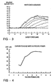
- Figure 3 is a representation of the relative reflectivity at different lasers powers of a material encompassed by the claims of the present invention.
- a material having a composition Te 53 Ge 37 Se 10 can exhibit a relative reflectivity between the unrecorded and recorded state of approximately 2.5 when the record laser power is at least 6 or 7 milliwatts.
- Figure 3 shows that the threshold record power using a laser pulse width of 100 nanoseconds is 6 to 7 milliwatts.
- the material of the present invention will switch from a first detectable state to a second detectable state upon the application of a recording laser pulse having a power of 6 to 7 milliwatts in a 100 nanosecond pulse.
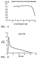
- Figures 4 and 5 are, respectively, graphs showing the plot of carrier to noise ratio versus, respectively, the record power and the record frequency for the Te 53 Ge 37 Se 10 material.
- a disk coated with this material shows over 53 dB carrier to noise ratio when recorded on at a laser power of 5.5 milliwatts (10 meters per second linear track velocity), as can be seen in Figure 4.
- Figure 5 shows that this same material has a usable upper frequency of greater than 5 MHz at 10 m/s LTV, corresponding to a bit length of 0.84 microns. Since the frequency during testing was essentially determined by the limits of the optics of the dynamic tester used, it is expected that the fundamental resolution of the material of the present invention may be higher.
- the following table shows experimentally determined crystallization temperatures for a range of compositions within the TeGeSb system.
- the material having a composition Te 53 Ge 37 Se 10 exhibited a crystallization temperature of 218° C.
- the thermal stability of optical films utilizing material of the present invention at 50° C. to be at least several decades.
- a bulk alloy having a nominal composition of Te 51 Ge 40 Sb 9 and encompassed by the claims of the present invention was prepared.
- the bulk alloy was prepared by grinding together appropriate amounts of tellurium, germanium and antimony. This mixture was placed in a quartz ampule, which was subsequently evacuated and sealed. The ampule was heated at 850 C. for 1 1/2 hours, with a rocking motion used for agitation throughout the heating step. The alloy was cooled by a water quench, and the ampule then opened. It was then ground to a particle size of approximately 1/6 of a millimeter. A measured amount of the alloy was deposited by vacuum evaporation using a source temperature of approximately 520 C.
- the bulk alloy described above has two phases, as revealed by x-ray diffraction studies and electron dispersive spectroscopy.
- the major phase has a composition of Te 52 Ge 37 Sb 11 , which can be considered, within experimental error, to be the same composition as that of the bulk alloy.
- a second, minor phase having a nominal composition Te 51 Ge 44 Sb 5 .
- the two phases have substantially similar crystallization temperatures and kinetics.
- the results of Auger electron spectroscopy and electron dispersive spectroscopy for the major phase of the material are shown, respectively, in Figures 8 and 9.
- Auger electron spectroscopy is a particular useful analytical tool for thin films deposited from a bulk source.
- compositions within the TAG ternary system that form crystals including all three elements and having a composition similar to the composition of the bulk material.
- the following composition will consistently crystallize from materials having elemental ratios of Te:Ge:Sb in this vicinity:
Abstract
Description
- The invention disclosed herein relates to data storage devices where data is stored in a material that is reversibly switchable between detectable states in response to the input of energy.
- Nonablative state changeable data storage systems, for example, optical data storage systems, record information in a state changeable material that is switchable between at least two detectable states by the application of energy such as, for example, projected optical beam energy, electrical energy, or thermal energy, thereto.
- State changeable data storage material is typically incorporated in a data storage device having a structure such that the data storage material is supported by a substrate and protected by encapsulants. In the case of optical data storage devices, the encapsulants include, for example, anti-ablation materials and layers, thermal insulation materials and layers, anti-reflection materials and layers, reflective layers, and chemical isolation layers. Moreover, various layers may perform more than one of these functions. For example, anti-reflection layers may also be anti-ablation layers and thermal insulating layers. The thicknesses of the layers, including the layer of state changeable data storage material, are engineered to minimize the energy necessary for effecting the state change and to optimize the high contrast ratio, high carrier to noise to ratio, and high stability of state changeable data storage materials.
- The state changeable material is a material capable of being switched from one detectable state to another detectable state or states by the application of, for example, projected beam energy, electrical energy, or thermal energy thereto. The detectable states of state changeable materials may differ in their morphology, surface topography, relative degree of order, relative degree of disorder, electrical properties, optical properties, including indices of refraction and reflectivity, or combinations of one or more of the foregoing. The state of the state changeable material is detectable by properties such as, for example, the electrical conductivity, electrical resistivity, optical transmissivity, optical absorption, optical refraction, optical reflectivity, or combinations thereof. That is, the magnitude of the detectable property will vary in a predictable manner as the state changeable material changes state.
- Formation of the data storage device includes deposition of the individual layers by, for example, evaporative deposition, chemical vapor deposition, and/or plasma deposition. As used herein plasma deposition includes sputtering, glow discharge, and plasma assisted chemical vapor deposition.
- Tellurium based materials have been utilized as state changeable materials for data storage where the state change is a structural change evidenced by a change in a physical property such as reflectivity. This effect is described, for example, in J. Feinleib, J. deNeufville, S.C. Moss, and S.R. Ovshinsky, "Rapid Reversible Light-Induced Crystallization of Amorphous Semiconductors," "Appl. Phys. Lett., Vol. 18(6), pages 254-257 (Mar. 15, 1971), and in U.S. Pat. No. 3,530,441 to S.R. Ovshinsky for Method and Apparatus For Storing And Retrieving Of Information.
- Tellurium based state changeable materials, in general, are single or multi-phased systems and: (1) the ordering phenomena include a nucleation and growth process (including both or either homogeneous and heterogeneous nucleations) to convert a system of disordered materials to a system of ordered and disordered materials; and (2) the vitrification phenomena include melting and rapid quenching of the phase changeable material to transform a system of disordered and ordered materials to a system of largely disordered materials. The above phase changes and separations occur over relatively small distances, with intimate interlocking of the phases and gross structural discrimination, and are highly sensitive to local variations in stoichiometry.
- In chalcogenide type memory materials, the measures of performance include (1) the contrast ratio, that is, the difference in reflectivities of the states divided by the sums of the reflectivities of the states, and (2) the carrier to noise ratios of both (a) the "written" and (b) the "erased" states. The failure mode of the memory material is evidenced by the deterioration in the measures of performance with respect to the number of cycles. That is, failure may be evidenced by for example (1) a reduction in contrast ratio with increasing cycles, or by (2) a reduction in the written carrier to noise ratio or an increase in the erased carrier to noise ratio.
- If the memory material is to be used as a "write once" medium, it is highly desirable that it have a relatively high glass transition temperature since this gives it good thermal stability over the life of the recording medium. Since, in many cases, it is customary to write or record onto a medium which is already in an amorphous first state by switching it to crystalline second state, the integrity of the recording depends on the ability of the amorphous second state to resist spontaneous or accidental crystallization into the written state. The higher the glass transition temperature of the recording medium is, the more likely the medium will resist undesirable crystallization when in the amorphous state, particularly when the recorded region consists of all alternating regions of recorded crystalline spots and un-altered amorphous species between. Of course, the crystallization temperature must not be so high or that recording sensitivity suffers.
- In addition to write once materials, optical data storage systems may also employ erasable material which may be recorded upon, erased, rerecorded upon, re-erased, etc. In this case, the phase changeable material must reversibly be able to change from the amorphous to the crystalline state, and back again, repeatedly. For erasable materials, additional considerations are important. Most significantly, through repeated cycle life (repeated vitrification and crystallization), prior art materials have shown a tendency to degrade over time. It is thought that important factors contributing to this degradation over cycle life are the tendency for inhomogeneities and inclusions to appear in the material. That is, after the material crystallizes and recrystallizes, regions of variable structure and composition may appear therein which were not present in the original material. Due to the thermal history of the material, the various components of which it is composed may selectively migrate, chemically bond, or substitute for other components in the crystal lattice. Moreover, some of the material may not properly vitrify, thus creating undesirable crystalline or non-crystalline inclusions. All of these factors can result in degraded performance.
- These problems become particularly acute in typical tellurium based materials, such as tellurium-antimony-germanium systems because, depending upon the atomic percentages of each individual component within the material, these TAG systems can form a multitude of crystalline and amorphous phases. Thus, even though the as deposited material has a nominal composition of Tex Gey Sbz, the material, in its crystalline state, may comprise a plurality of crystalline phases of varying and unpredictable composition. That is, one crystalline phase may have proportionately much more tellurium, another much more germanium, etc. Because of this noncongruency of composition between the amorphous and crystalline states, such materials are prone to degrade over cycle life due to the reasons explained above.
- Furthermore, due to the multitude of crystalline phases, switching to the crystalline state includes atomic diffusion and is therefore relatively slow. Thus, switching speed is undesirably slow, and selecting a new composition to improve switching speed may compromise and the thermal stability of the material.
- The desirability of congruency in composition between the crystalline and amorphous states has been described with respect to a binary optical memory material in U.S. Patent Nos. 4,876,667 and 4,924,436, both assigned to assignee of the present invention. Both referenced patents concern themselves with binary chalcogenide data storage material, namely antimony telluride/antimony selenide compositions. As described in the referenced patents, the telluride and the selenide are essentially compositionally congruent between the amorphous and crystalline states. This is so because the telluride/selenide compositions are substantially miscible in substantially all proportions. That is, each crystal has approximately the nominal composition of the as deposited material. This is so largely because, due to their atomic structure and valence characteristics, the tellurides and selenides are capable of substituting for each other in the crystal lattice over a wide range of compositions. However, this is known not to be the case for TeGeSb systems.
- The desirability of maintaining compositional congruency while depositing the layer of memory material in tellurium-based memory materials has been recognized. See, for example, U.S. Patent No. 4,621,032, assigned to the assignee of the present invention. The reference discloses a method of depositing the layer of memory material by a congruent sublimation process wherein the sources or precursor materials are selected so as to maintain consistency in the deposited materials. However, this patent also teaches that there can be phase separation upon crystallization of the amorphous material into a crystalline and amorphous second phase, which phase separation necessarily entails the undesirable consequences noted above.
- The article "Ge-Te-Sb Based Overwritable phase change Optical Dick" in Soc. Int. Symp. on Optical Memory, 1989 discloses binary chalcogenide alloy systems.
- Disclosed and claimed herein is a state changeable memory alloy changeable from a first state to a second state in response to the input of energy, said alloy having a first detectable characteristic when in said first state and a second detectable characteristic when in said second state, and said first and second detectable characteristics selected from the group consisting of reflectivity, band gap, electrical resistance, optical absorption, magnetic susceptibility and thermal conductivity, wherein said first state is a disordered phase, said alloy being a chalcogenide material, and being
characterized in that
said alloy comprises at least three individually combined elements forming at least a ternary system, having a single phase first state and said second state comprises either - (1) a single phase second state of the same composition as said first state so
that said first and said second state are chemically congruent,
or - (2) a plurality of second phases having similar crystallization temperatures and kinetics, including a main phase which is chemically congruent with said first phase.
-
- The memory alloy of the present invention is a chalcogenide, optical memory alloy which exhibits compositional congruency between an amorphous and a crystalline state. The alloy material has a first detectable characteristic (typically, optical reflectivity) when in the amorphous state and a second detectable characteristic when it is in the crystalline state. By using the method in a multilayer thin film optical structure, die direction of reflectivity change can be selected by appropriate choice of the memory material layer and other layer thicknesses. The material is capable of undergoing a congruent state change upon the application of projected beam energy thereto, most particularly, beam energy in the form of a laser beam.
- In a write-once system, the material, which is typically amorphous in its as-deposited condition, may be switched typically only once into its crystalline state by a single application of laser light at an energy sufficient to crystallize or initiate crystallization of the material. In this manner, data is recorded onto the material. Alternatively, the material may be written on by switching it from the crystalline to the amorphous state. In erasable systems, the material must be capable of undergoing repeated switching between one state and another. In order to do this, the material is written on by crystallizing (or vitrifying) it with a laser beam at a first energy, and revitrified (or recrystallized) by erasing it with laser light of a second different energy. See, for example, U.S. Patent Nos. 4,667,309 and 4,744,055, both assigned to the assignee of the present invention.
- The material claimed herein has the following composition:
TeaGebSbc
a, b and c being expressed in atomic percentages. A, b and c are selected such that the material maintains compositional congruency between the crystalline and amorphous states. More particularly, when the material is in the crystalline state it includes a major portion which has substantially the same composition as the material has when in the amorphous state and a minor portion which has the following composition:
TedGeeSbf
d, e and f again being expressed in atomic percentages. The composition of the minor portion is not too far off the composition of the major portion. More particularly, the difference between a and d, b and e, and c and f total no more than 16 atomic percent. Thus, the amount of any single element in the minor portion can vary from the amount of the same element in the major portion by no more than 8 atomic percent. - A, b and c must be carefully selected in order to maintain the compositional congruency of the alloy between states. In particular, it has been found that compositional congruency is maintained if a is kept between 49 and 53, b is between 36 and 40, and c is between 7 and 11. It is also believed that compositional congruency is maintained when, for example, the following limitations are observed:
- Te 47-53 Ge 48-43 Sb 3-7 or
- Te 47-53 Ge 31-36 Sb 15-21 or
- Te 47-53 Ge 15-21 Sb 31-36
-
- Also claimed is a data carrier utilizing the alloy material described above. The carrier comprises a substrate, a dielectric first encapsulating layer on the substrate, a memory layer formed of the alloy on the dielectric first encapsulating layer and a dielectric second encapsulating layer atop the memory layer. Optionally it may further include an optically reflective layer, preferably of antimony, between the alloy layer and the second encapsulating layer.
- The data storage medium may be formed by depositing the materials to form a substantially uniform deposit thereof. The thickness of the deposit is chosen to give reflectivity and contrast as deemed best by the application.
- This invention may be more particularly understood by reference to the following drawings in which:
- FIGURE 1 is a partial cut-away isometric view, not to scale, with exaggerated latitudinal dimensions and vertical scale, of an optical data storage device constructed in accord with the teachings of the present invention;
- FIGURE 2 is a detailed section of a part of the optical data storage device of FIGURE 1 showing the relationship of the various layers thereof;
- FIGURE 3 is a representation of the relative reflectivity obtained by exposure to different laser powers at various pulse widths of a material encompassed by the claims of the present invention;
- FIGURE 4 is a graph showing the plot of the carrier-to-noise ratio versus the laser power used to make a recording on a material encompassed by the claims of the present invention;
- FIGURE 5 is a graph with carrier-to-noise ratio plotted versus the record frequency for recordings made on a material encompassed by the claims of the present invention;
- FIGURE 6 is a graph showing the rate of deposition of a material encompassed by the claims of the present invention evaporated from a TeGeSb alloy source plotted against time;
- FIGURE 7 is a representation of an Auger electron spectroscopy profile of a material encompassed by the claims of the present invention;
- FIGURE 8 is another Auger electron spectroscopy profile of another material encompassed by the claims of the invention; and
- FIGURE 9 is a representation of an x-ray diffraction spectroscopy profile of the material of FIGURE 8.
-
- Throughout the following detailed description, like reference numerals are used to refer to the same element shown in multiple figures thereof.
- Figures 1 and 2 show a projected beam
data storage device 1 having a substrate, for example aplastic substrate 11, a firstencapsulating dielectric layer 21, for example a first germanium oxide encapsulating layer, a chalcogenide compound datastorage medium layer 31, an antimony reflective layer 35, a second dielectric layer e.g., a secondgermanium oxide layer 41, and a second substrate, e.g.,plastic substrate 51. - Figure 2 shows a section of the
data storage device 1 of Figure 1 in greater detail. As there shown, thesubstrate 11 is a polymeric sheet, for example a polycarbonate sheet. Thesubstrate 11 is a substantially optically invariant, optically isotropic, transparent sheet. The preferred thickness is of about 1.2 mm. - A
top substrate 51 andencapsulant layer 41 is a film, sheet orlayer 49, e.g. a photoinitiated polymerized acrylic sheet. Polymerized, molded, injection molded, or cast into thepolymeric sheet 11, may be grooves. When grooves are present they may have a thickness from about 500 to about 1000 Angstroms. The film, sheet, orlayer 49 may act as an adhesive layer holding thesubstrate 51 to theencapsulant 41. It has a thickness of from about 1 to about 200 microns and preferably from about 10 to about 100 microns. - Deposited atop the
substrate 11 is adielectric barrier layer 21. A similardielectric encapsulating layer 41 lies betweensheet 49 and optional antimony layer 35. The dielectric barrier layers 21, 41, for example, of germanium oxide, are each from about 500 to about 2000 Angstroms thick. Preferably they have an optical thickness of one-quarter times the laser wavelength times the index of refraction of the material forming thedielectric layers active layer 31 and/or prevent the plastic substrates from deforming due to local heating of thechalcogenide layer 31, e.g., during recording or erasing. - Other dielectrics may provide the encapsulating layers 21,41. For example, the encapsulating layers may be silica, alumina, silicon nitride, or other dielectric. The composition of any of these materials may be layered or graded to avoid diffusion into the
chalcogenide layer 31. - The chalcogenide compound data
storage medium layer 31 is comprised of a congruent state changeable material which is capable of existing in at least an amorphous state and a crystalline state. The material has a first detectable characteristic, such as optical reflectivity, when in the crystalline state, and a second detectable characteristic, again such as optical reflectivity, when in the amorphous state. In one adaptation, thechalcogenide memory layer 31 is used as an anti-reflection coating for the antimony layer 35. The optical constants of the two layers are such that the thickness of the chalcogenide layer is chosen to be very thin (about 300 angstroms) to achieve maximum reflectivity contrast. Because thechalcogenide layer 31 is only partially transmissive, the contribution of the antimony layer 35 to the total reflectivity increases when thechalcogenide layer 31 is thinner, which improves the contrast. The thickness of the antimony layer 35 is not as important, but best results are obtained when it is at least thick enough (also about 300 angstroms) to obtain its maximum reflectivity. When phase change chalcogenide alloy films are used in an anti-reflection optical structure, the direction of reflectivity change can be selected by appropriate choice of the chalcogenide layer thickness. In this case, the layer thickness is selected such that there is a measurable increase in reflectivity after the material has been crystallized. Typically, the reflectivity of the material after recording is 1 1/2 to 3 times that of the unrecorded spot, or even more. The antimony layer 35 also functions as a seed layer to initiate crystallization in thechalcogenide layer 31 when it is switched to the crystallized state. In this way, switching speed is increased. - In general, it has been found that optimum material performance in terms of switching speed is achieved when tellurium comprises approximately 50 atomic percent of the material and germanium together with either antimony, bismuth or tin comprises the remainder. The generic formula for this improved material may be written Te50(GeX)50 where X equals Sb, Bi or Sn, it being understood that several percent deviation from the general formula may be tolerated without significant effect.
- The Te-Ge system forms a rhombohedral crystalline phase and it is speculated that when the (GeX) component is in an approximate 1:1 ratio with the Te, the crystal structure becomes face centered cubic and reversible, high speed switching is achieved.
- In general, some germanium must be present to assure that the desired TeGe phase is developed; however, it has been found that Sb, Sn, Bi and the like may substitute for a significant portion of the Ge while preserving the desired morphology.
- One particular class of materials comprise Te50(GeSb)50 it has been found that in those instances where the Ge is present in a greater amount than the Sb, the material crystallizes into two phases having similar crystallization temperatures and kinetics. In those instances where the Sb is present in a higher amount than the Ge, crystallization tends to produce one phase. It has been found that the TeSb tends to produce non-equilibrium crystalline phases. In accord with the present invention, it has been found that presence of Ge in the system stabilizes the Te-Sb phase and enables the congruent crystallization of the material from the amorphous state.
- The material of
chalcogenide layer 31 is capable of undergoing a congruent state change upon the application of projected beam energy such as laser energy thereto. The material is a compound having the composition TeaGebSbc, a, b and c being expressed in atomic percentages and selected such that, when the material is in the crystalline state, the material is substantially crystalline and includes a major crystal phase which has the same composition as the material has when in the amorphous state. The crystalline material may further includes a minor portion which has the composition TedGeeSbf, d, e and f being expressed in atomic percentages, wherein the differences between a and d, b and e, and c and f respectively total not more than 16 atomic percent. - After experimenting with a range of optical recording film compositions, it has been experimentally determined that, where a is from 49 to 53 atomic percent, b is from 35 to 43 atomic percent and c is from 7 to 11 atomic percent, the compositions exhibit optimum performance when tested for sensitivity, and crystallization temperature, Tx.
- Figure 3 is a representation of the relative reflectivity at different lasers powers of a material encompassed by the claims of the present invention. As shown in Figure 3, a material having a composition Te53Ge37Se10 can exhibit a relative reflectivity between the unrecorded and recorded state of approximately 2.5 when the record laser power is at least 6 or 7 milliwatts. Figure 3 shows that the threshold record power using a laser pulse width of 100 nanoseconds is 6 to 7 milliwatts. As can be seen, the material of the present invention will switch from a first detectable state to a second detectable state upon the application of a recording laser pulse having a power of 6 to 7 milliwatts in a 100 nanosecond pulse.
- Figures 4 and 5 are, respectively, graphs showing the plot of carrier to noise ratio versus, respectively, the record power and the record frequency for the Te53Ge37Se10 material. A disk coated with this material shows over 53 dB carrier to noise ratio when recorded on at a laser power of 5.5 milliwatts (10 meters per second linear track velocity), as can be seen in Figure 4.
- Figure 5 shows that this same material has a usable upper frequency of greater than 5 MHz at 10 m/s LTV, corresponding to a bit length of 0.84 microns. Since the frequency during testing was essentially determined by the limits of the optics of the dynamic tester used, it is expected that the fundamental resolution of the material of the present invention may be higher.
- The following table shows experimentally determined crystallization temperatures for a range of compositions within the TeGeSb system. In particular, the material having a composition Te53Ge37Se10 exhibited a crystallization temperature of 218° C.
Sample Number Composition Tx Te Ge Sb E-1043 25 60 15 >250° C E-1045 30 55 15 >250° C E-1036 35 50 15 >250° C E-1038 40 45 15 >250° C E-1039 45 40 15 >250° C E-1051 50 35 15 208° C E-1041 55 30 15 181° C E-1044 60 25 15 178° C E-1046 45 30 25 222° C E-1047 47 33 20 222° C E-1048 53 37 10 218° C E-1049 36 39 5 201° C - Further experiments were conducted to determine the structure of one species of the claimed material. A bulk alloy having a nominal composition of Te51Ge40Sb9 and encompassed by the claims of the present invention was prepared. The bulk alloy was prepared by grinding together appropriate amounts of tellurium, germanium and antimony. This mixture was placed in a quartz ampule, which was subsequently evacuated and sealed. The ampule was heated at 850 C. for 1 1/2 hours, with a rocking motion used for agitation throughout the heating step. The alloy was cooled by a water quench, and the ampule then opened. It was then ground to a particle size of approximately 1/6 of a millimeter. A measured amount of the alloy was deposited by vacuum evaporation using a source temperature of approximately 520 C. The deposition was continued until the material in the deposition crucible was exhausted. As can be seen in Figure 6, it was found that the deposition rate versus time for this congruently state changeable material is linear, which is a necessary characteristic of a constant-composition sublimation (See U.S. Patent No. 4,621,032). A silicon wafer was exposed to the evaporant stream during the deposition. Figure 7 is an Auger electron spectroscopy profile which confirms that the composition of the deposited material is constant throughout the deposition.
- The bulk alloy described above has two phases, as revealed by x-ray diffraction studies and electron dispersive spectroscopy. The major phase has a composition of Te52Ge37Sb11, which can be considered, within experimental error, to be the same composition as that of the bulk alloy. Also present is a second, minor phase having a nominal composition Te51Ge44Sb5. The two phases have substantially similar crystallization temperatures and kinetics. The results of Auger electron spectroscopy and electron dispersive spectroscopy for the major phase of the material are shown, respectively, in Figures 8 and 9. Auger electron spectroscopy is a particular useful analytical tool for thin films deposited from a bulk source. Because of its depth profile and capabilities, it is possible to determine the composition of a film as it is being eroded away by ion milling. Thus, not only can the composition of the film be determined, but it can be seen how the composition changes over the depth of the film. As can be seen from Figure 8, beyond the first few tens of angstroms ( which reflects contaminants that are introduced to the surface during normal sampling handling and storage), the composition of the film remains remarkedly consistent over the entire depth thereof.
- It is believed that there are other distinct compositions within the TAG ternary system that form crystals including all three elements and having a composition similar to the composition of the bulk material. For example, the following composition will consistently crystallize from materials having elemental ratios of Te:Ge:Sb in this vicinity:
- Te51 Ge44 Sb5
- Te51 Ge32 Sb17
- Te51 Ge17 Sb32 Again, it is expected that materials of this composition will exhibit superior performance characteristics.
-
- It is, of course, possible that other ratios of the elements within the TAG ternary system may meet the limitations of the claims appended hereto. Furthermore, while the present invention has been described with respect to optical memory systems, it is not limited to such systems; rather, it also finds application in any system where energy is applied to change the state of the material in a predictable manner. Specifically, the memory material of the present invention may be utilized in a system wherein electrical energy or thermal energy is applied to the material to effect the state change. While the invention has been described with reference to a particular exemplifications and embodiments thereof, it is not intended to be limited to the exemplification and embodiments described. Rather, it is the claims appended hereto and all reasonable equivalents thereof which define the true scope of the present invention.
Claims (12)
- A state changeable memory alloy changeable from a first state to a second state in response to the input of energy, said alloy having a first detectable characteristic when in said first state and a second detectable characteristic when in said second state, and said first and second detectable characteristics selected from the group consisting of reflectivity, band gap, electrical resistance, optical absorption, magnetic susceptibility and thermal conductivity, wherein said first state is a disordered phase, said alloy being a chalcogenide material, and being
characterized in that
said alloy comprises at least three individually combined elements forming at least a ternary system, having a single phase first state and said second state comprises either(1) a single phase second state of the same composition as said first state so that said first and said second state are chemically congruent,
or(2) a plurality of second phases having similar crystallization temperatures and kinetics, including a main phase which is chemically congruent with said first phase. - A state changeable memory alloy as claimed in claim 1, said alloy comprising at least Te, Ge and Sb,
characterized in that
said alloy has the general formula TeaGebSbc, wherein a is between 47 and 53, and(i) b is between 31 and 36 and c is between 15 and 21, or(ii) b is between 15 and 21 and c is between 31 and 36, or(iii) b is between 35 and 49 and c is between 3 and 11. - An alloy as claimed in claim 2,
characterized in that
said alloy has the general formula TeaGebSbc, wherein a is between 49 and 53, b is between 36 and 40 and c is between 7 and 11. - An alloy as claimed in claim 2,
characterized in that
said alloy has the general formula TeaGebSbc, wherein a is between 47 and 53, b is between 43 and 48 and c is between 3 and 7. - An alloy as claimed in claim 2,
characterized in that
said alloy has the general formula TeaGebSbc, wherein a is between 49 and 53 and b is between 35 and 43 and c is between 7 and 11. - An alloy as claimed in one of the preceding claims,
characterized in that
said alloy has the formula TeaGebSbc wherein a, b and c are selected such that, when said material is in the crystalline state, it is substantially entirely crystalline and includes a major portion which has the same composition as the material has when in the amorphous state and a minor portion which has the composition TedGeeSbf, wherein d, e and f are not too far off a, b and c, respectively. - An alloy as claimed in claim 6,
characterized in that
the differences between a and d, b and e and c and f, respectively, total no more than 16. - A state changeable memory alloy as claimed in claim 1,
characterized in that
said alloy has the formula Te50(GeX)50 wherein X is Sn or Bi. - An alloy as claimed in one of the preceding claims,
characterized in that
said first state is an amorphous state and said second state is a crystalline state. - An alloy as claimed in one of the preceding claims,
characterized in that
said alloy is capable of changing from said first state to said second state in response to the input of optical, electrical or thermal energy. - A data carrier having an alloy as claimed in one of the preceding claims, and
including a substrate (11), a dielectric first encapsulating layer (21) on the substrate (11),
a memory layer (31) on the dielectric first encapsulating layer (21) and
a dielectric second encapsulating layer (41) atop the memory layer (31), wherein the memory layer (31) is a non-ablative, congruent state change memory layer consisting of said alloy. - A carrier as claimed in claim 11,
characterized in that
an antimony layer (35) is placed in between said memory layer (31) and said second encapsulating layer (41) for initiating crystallization in said memory layer (31) and to contribute to the total reflectivity.
Priority Applications (1)
| Application Number | Priority Date | Filing Date | Title |
|---|---|---|---|
| EP99108310A EP0951011A1 (en) | 1991-02-15 | 1992-02-14 | Congruent state changeable optical memory material and device |
Applications Claiming Priority (2)
| Application Number | Priority Date | Filing Date | Title |
|---|---|---|---|
| US07/657,170 US5128099A (en) | 1991-02-15 | 1991-02-15 | Congruent state changeable optical memory material and device |
| US657170 | 1991-02-15 |
Related Child Applications (1)
| Application Number | Title | Priority Date | Filing Date |
|---|---|---|---|
| EP99108310A Division EP0951011A1 (en) | 1991-02-15 | 1992-02-14 | Congruent state changeable optical memory material and device |
Publications (3)
| Publication Number | Publication Date |
|---|---|
| EP0499273A2 EP0499273A2 (en) | 1992-08-19 |
| EP0499273A3 EP0499273A3 (en) | 1994-06-01 |
| EP0499273B1 true EP0499273B1 (en) | 2002-11-13 |
Family
ID=24636116
Family Applications (2)
| Application Number | Title | Priority Date | Filing Date |
|---|---|---|---|
| EP99108310A Withdrawn EP0951011A1 (en) | 1991-02-15 | 1992-02-14 | Congruent state changeable optical memory material and device |
| EP92102513A Expired - Lifetime EP0499273B1 (en) | 1991-02-15 | 1992-02-14 | Congruent state changeable optical memory alloy and data carrier |
Family Applications Before (1)
| Application Number | Title | Priority Date | Filing Date |
|---|---|---|---|
| EP99108310A Withdrawn EP0951011A1 (en) | 1991-02-15 | 1992-02-14 | Congruent state changeable optical memory material and device |
Country Status (8)
| Country | Link |
|---|---|
| US (1) | US5128099A (en) |
| EP (2) | EP0951011A1 (en) |
| JP (2) | JPH04337532A (en) |
| KR (1) | KR100245901B1 (en) |
| AT (1) | ATE227878T1 (en) |
| CA (1) | CA2061187C (en) |
| DE (1) | DE69232844T2 (en) |
| TW (1) | TW279903B (en) |
Families Citing this family (104)
| Publication number | Priority date | Publication date | Assignee | Title |
|---|---|---|---|---|
| US5233599A (en) * | 1990-03-14 | 1993-08-03 | Matsushita Electric Industrial Co., Ltd. | Optical disk with a recording layer composed of tellurium, antimony, and germanium |
| JP2556183B2 (en) * | 1990-09-11 | 1996-11-20 | 富士ゼロックス株式会社 | Optical recording method and optical recording medium using this method |
| JPH07141693A (en) * | 1993-09-22 | 1995-06-02 | Toshiba Corp | Information recording medium |
| US5458941A (en) * | 1994-06-09 | 1995-10-17 | Minnesota Mining And Manufacturing Company | Optical recording medium exhibiting eutectic phase equilbria |
| WO1996011471A1 (en) * | 1994-10-05 | 1996-04-18 | Asahi Kasei Kogyo Kabushiki Kaisha | Phase change mode optical disk and method of manufacturing the same |
| US5583734A (en) * | 1994-11-10 | 1996-12-10 | Raychem Corporation | Surge arrester with overvoltage sensitive grounding switch |
| KR100668180B1 (en) * | 1996-03-11 | 2007-01-11 | 마츠시타 덴끼 산교 가부시키가이샤 | Optical data recording medium, method of producing the same and method of reproducing/erasing record |
| US6821707B2 (en) | 1996-03-11 | 2004-11-23 | Matsushita Electric Industrial Co., Ltd. | Optical information recording medium, producing method thereof and method of recording/erasing/reproducing information |
| AU724629B2 (en) * | 1997-04-16 | 2000-09-28 | Asahi Kasei Kabushiki Kaisha | Process for producing optical information recording medium and optical information recording medium produced by the process |
| US6503690B1 (en) * | 1997-08-12 | 2003-01-07 | Matsushita Electric Industrial Co., Ltd. | Optical information recording medium, method for producing the same, and method for recording and reproducing optical information |
| JPH11134720A (en) | 1997-08-28 | 1999-05-21 | Matsushita Electric Ind Co Ltd | Optical information recording medium and its recording/ reproducing method |
| US6343062B1 (en) | 1997-09-26 | 2002-01-29 | Matsushita Electric Industrial Co., Ltd | Optical disk device and optical disk for recording and reproducing high-density signals |
| TW448443B (en) * | 1998-08-05 | 2001-08-01 | Matsushita Electric Ind Co Ltd | Optical information storage media and production method as well as the storage reproducing method and device |
| US7260051B1 (en) | 1998-12-18 | 2007-08-21 | Nanochip, Inc. | Molecular memory medium and molecular memory integrated circuit |
| TW484126B (en) | 1999-03-26 | 2002-04-21 | Matsushita Electric Ind Co Ltd | Manufacturing and recording regeneration method for information record medium |
| US6580683B1 (en) | 1999-06-23 | 2003-06-17 | Dataplay, Inc. | Optical recording medium having a master data area and a writeable data area |
| US7227817B1 (en) | 1999-12-07 | 2007-06-05 | Dphi Acquisitions, Inc. | Low profile optical head |
| US7191153B1 (en) | 1999-09-10 | 2007-03-13 | Dphi Acquisitions, Inc. | Content distribution method and apparatus |
| US6631359B1 (en) | 1999-09-10 | 2003-10-07 | Dphi Acquisitions, Inc. | Writeable medium access control using a medium writeable area |
| US6638820B2 (en) | 2001-02-08 | 2003-10-28 | Micron Technology, Inc. | Method of forming chalcogenide comprising devices, method of precluding diffusion of a metal into adjacent chalcogenide material, and chalcogenide comprising devices |
| US6727192B2 (en) * | 2001-03-01 | 2004-04-27 | Micron Technology, Inc. | Methods of metal doping a chalcogenide material |
| US6734455B2 (en) | 2001-03-15 | 2004-05-11 | Micron Technology, Inc. | Agglomeration elimination for metal sputter deposition of chalcogenides |
| US7102150B2 (en) | 2001-05-11 | 2006-09-05 | Harshfield Steven T | PCRAM memory cell and method of making same |
| US6951805B2 (en) * | 2001-08-01 | 2005-10-04 | Micron Technology, Inc. | Method of forming integrated circuitry, method of forming memory circuitry, and method of forming random access memory circuitry |
| US6737312B2 (en) | 2001-08-27 | 2004-05-18 | Micron Technology, Inc. | Method of fabricating dual PCRAM cells sharing a common electrode |
| US6881623B2 (en) | 2001-08-29 | 2005-04-19 | Micron Technology, Inc. | Method of forming chalcogenide comprising devices, method of forming a programmable memory cell of memory circuitry, and a chalcogenide comprising device |
| US6784018B2 (en) | 2001-08-29 | 2004-08-31 | Micron Technology, Inc. | Method of forming chalcogenide comprising devices and method of forming a programmable memory cell of memory circuitry |
| US6955940B2 (en) * | 2001-08-29 | 2005-10-18 | Micron Technology, Inc. | Method of forming chalcogenide comprising devices |
| US20030047765A1 (en) * | 2001-08-30 | 2003-03-13 | Campbell Kristy A. | Stoichiometry for chalcogenide glasses useful for memory devices and method of formation |
| US7113474B2 (en) * | 2001-09-01 | 2006-09-26 | Energy Conversion Devices, Inc. | Increased data storage in optical data storage and retrieval systems using blue lasers and/or plasmon lenses |
| US6815818B2 (en) | 2001-11-19 | 2004-11-09 | Micron Technology, Inc. | Electrode structure for use in an integrated circuit |
| US6791859B2 (en) | 2001-11-20 | 2004-09-14 | Micron Technology, Inc. | Complementary bit PCRAM sense amplifier and method of operation |
| US6873538B2 (en) * | 2001-12-20 | 2005-03-29 | Micron Technology, Inc. | Programmable conductor random access memory and a method for writing thereto |
| US6909656B2 (en) * | 2002-01-04 | 2005-06-21 | Micron Technology, Inc. | PCRAM rewrite prevention |
| US20030143782A1 (en) * | 2002-01-31 | 2003-07-31 | Gilton Terry L. | Methods of forming germanium selenide comprising devices and methods of forming silver selenide comprising structures |
| US6867064B2 (en) | 2002-02-15 | 2005-03-15 | Micron Technology, Inc. | Method to alter chalcogenide glass for improved switching characteristics |
| US6791885B2 (en) | 2002-02-19 | 2004-09-14 | Micron Technology, Inc. | Programmable conductor random access memory and method for sensing same |
| US7151273B2 (en) | 2002-02-20 | 2006-12-19 | Micron Technology, Inc. | Silver-selenide/chalcogenide glass stack for resistance variable memory |
| US6809362B2 (en) | 2002-02-20 | 2004-10-26 | Micron Technology, Inc. | Multiple data state memory cell |
| US7087919B2 (en) | 2002-02-20 | 2006-08-08 | Micron Technology, Inc. | Layered resistance variable memory device and method of fabrication |
| US6891749B2 (en) * | 2002-02-20 | 2005-05-10 | Micron Technology, Inc. | Resistance variable ‘on ’ memory |
| US6937528B2 (en) | 2002-03-05 | 2005-08-30 | Micron Technology, Inc. | Variable resistance memory and method for sensing same |
| US6849868B2 (en) | 2002-03-14 | 2005-02-01 | Micron Technology, Inc. | Methods and apparatus for resistance variable material cells |
| US6855975B2 (en) | 2002-04-10 | 2005-02-15 | Micron Technology, Inc. | Thin film diode integrated with chalcogenide memory cell |
| US6864500B2 (en) | 2002-04-10 | 2005-03-08 | Micron Technology, Inc. | Programmable conductor memory cell structure |
| US6858482B2 (en) | 2002-04-10 | 2005-02-22 | Micron Technology, Inc. | Method of manufacture of programmable switching circuits and memory cells employing a glass layer |
| US6825135B2 (en) | 2002-06-06 | 2004-11-30 | Micron Technology, Inc. | Elimination of dendrite formation during metal/chalcogenide glass deposition |
| US6890790B2 (en) | 2002-06-06 | 2005-05-10 | Micron Technology, Inc. | Co-sputter deposition of metal-doped chalcogenides |
| US7015494B2 (en) * | 2002-07-10 | 2006-03-21 | Micron Technology, Inc. | Assemblies displaying differential negative resistance |
| JP4027282B2 (en) * | 2002-07-10 | 2007-12-26 | キヤノン株式会社 | Inkjet recording head |
| US7209378B2 (en) | 2002-08-08 | 2007-04-24 | Micron Technology, Inc. | Columnar 1T-N memory cell structure |
| US7018863B2 (en) | 2002-08-22 | 2006-03-28 | Micron Technology, Inc. | Method of manufacture of a resistance variable memory cell |
| US6768666B2 (en) * | 2002-08-23 | 2004-07-27 | Energy Conversion Devices, Inc. | Phase angle controlled stationary elements for wavefront engineering of electromagnetic radiation |
| US6864521B2 (en) * | 2002-08-29 | 2005-03-08 | Micron Technology, Inc. | Method to control silver concentration in a resistance variable memory element |
| US6831019B1 (en) | 2002-08-29 | 2004-12-14 | Micron Technology, Inc. | Plasma etching methods and methods of forming memory devices comprising a chalcogenide comprising layer received operably proximate conductive electrodes |
| US7010644B2 (en) * | 2002-08-29 | 2006-03-07 | Micron Technology, Inc. | Software refreshed memory device and method |
| US7294527B2 (en) | 2002-08-29 | 2007-11-13 | Micron Technology Inc. | Method of forming a memory cell |
| US7364644B2 (en) | 2002-08-29 | 2008-04-29 | Micron Technology, Inc. | Silver selenide film stoichiometry and morphology control in sputter deposition |
| US6867114B2 (en) | 2002-08-29 | 2005-03-15 | Micron Technology Inc. | Methods to form a memory cell with metal-rich metal chalcogenide |
| US20040040837A1 (en) * | 2002-08-29 | 2004-03-04 | Mcteer Allen | Method of forming chalcogenide sputter target |
| US6867996B2 (en) * | 2002-08-29 | 2005-03-15 | Micron Technology, Inc. | Single-polarity programmable resistance-variable memory element |
| US7163837B2 (en) | 2002-08-29 | 2007-01-16 | Micron Technology, Inc. | Method of forming a resistance variable memory element |
| US6856002B2 (en) * | 2002-08-29 | 2005-02-15 | Micron Technology, Inc. | Graded GexSe100-x concentration in PCRAM |
| US7233517B2 (en) | 2002-10-15 | 2007-06-19 | Nanochip, Inc. | Atomic probes and media for high density data storage |
| US6985377B2 (en) * | 2002-10-15 | 2006-01-10 | Nanochip, Inc. | Phase change media for high density data storage |
| AU2003282323A1 (en) | 2002-12-19 | 2004-07-14 | Koninklijke Philips Electronics N.V. | Electric device comprising phase change material |
| US6813178B2 (en) | 2003-03-12 | 2004-11-02 | Micron Technology, Inc. | Chalcogenide glass constant current device, and its method of fabrication and operation |
| US7022579B2 (en) | 2003-03-14 | 2006-04-04 | Micron Technology, Inc. | Method for filling via with metal |
| US7050327B2 (en) | 2003-04-10 | 2006-05-23 | Micron Technology, Inc. | Differential negative resistance memory |
| US6930909B2 (en) * | 2003-06-25 | 2005-08-16 | Micron Technology, Inc. | Memory device and methods of controlling resistance variation and resistance profile drift |
| US6961277B2 (en) | 2003-07-08 | 2005-11-01 | Micron Technology, Inc. | Method of refreshing a PCRAM memory device |
| US7061004B2 (en) | 2003-07-21 | 2006-06-13 | Micron Technology, Inc. | Resistance variable memory elements and methods of formation |
| US6903361B2 (en) | 2003-09-17 | 2005-06-07 | Micron Technology, Inc. | Non-volatile memory structure |
| US7153721B2 (en) * | 2004-01-28 | 2006-12-26 | Micron Technology, Inc. | Resistance variable memory elements based on polarized silver-selenide network growth |
| US7105864B2 (en) * | 2004-01-29 | 2006-09-12 | Micron Technology, Inc. | Non-volatile zero field splitting resonance memory |
| US7098068B2 (en) | 2004-03-10 | 2006-08-29 | Micron Technology, Inc. | Method of forming a chalcogenide material containing device |
| US7583551B2 (en) | 2004-03-10 | 2009-09-01 | Micron Technology, Inc. | Power management control and controlling memory refresh operations |
| US7301887B2 (en) * | 2004-04-16 | 2007-11-27 | Nanochip, Inc. | Methods for erasing bit cells in a high density data storage device |
| US7379412B2 (en) | 2004-04-16 | 2008-05-27 | Nanochip, Inc. | Methods for writing and reading highly resolved domains for high density data storage |
| US20050232061A1 (en) | 2004-04-16 | 2005-10-20 | Rust Thomas F | Systems for writing and reading highly resolved domains for high density data storage |
| US7354793B2 (en) | 2004-08-12 | 2008-04-08 | Micron Technology, Inc. | Method of forming a PCRAM device incorporating a resistance-variable chalocogenide element |
| US7326950B2 (en) | 2004-07-19 | 2008-02-05 | Micron Technology, Inc. | Memory device with switching glass layer |
| US7190048B2 (en) | 2004-07-19 | 2007-03-13 | Micron Technology, Inc. | Resistance variable memory device and method of fabrication |
| US7365411B2 (en) | 2004-08-12 | 2008-04-29 | Micron Technology, Inc. | Resistance variable memory with temperature tolerant materials |
| US7151688B2 (en) | 2004-09-01 | 2006-12-19 | Micron Technology, Inc. | Sensing of resistance variable memory devices |
| US7374174B2 (en) | 2004-12-22 | 2008-05-20 | Micron Technology, Inc. | Small electrode for resistance variable devices |
| US7317200B2 (en) | 2005-02-23 | 2008-01-08 | Micron Technology, Inc. | SnSe-based limited reprogrammable cell |
| US7709289B2 (en) | 2005-04-22 | 2010-05-04 | Micron Technology, Inc. | Memory elements having patterned electrodes and method of forming the same |
| US7427770B2 (en) | 2005-04-22 | 2008-09-23 | Micron Technology, Inc. | Memory array for increased bit density |
| US7269044B2 (en) | 2005-04-22 | 2007-09-11 | Micron Technology, Inc. | Method and apparatus for accessing a memory array |
| US7269079B2 (en) | 2005-05-16 | 2007-09-11 | Micron Technology, Inc. | Power circuits for reducing a number of power supply voltage taps required for sensing a resistive memory |
| US7463573B2 (en) | 2005-06-24 | 2008-12-09 | Nanochip, Inc. | Patterned media for a high density data storage device |
| US7367119B2 (en) | 2005-06-24 | 2008-05-06 | Nanochip, Inc. | Method for forming a reinforced tip for a probe storage device |
| US7309630B2 (en) * | 2005-07-08 | 2007-12-18 | Nanochip, Inc. | Method for forming patterned media for a high density data storage device |
| US7233520B2 (en) | 2005-07-08 | 2007-06-19 | Micron Technology, Inc. | Process for erasing chalcogenide variable resistance memory bits |
| US7274034B2 (en) | 2005-08-01 | 2007-09-25 | Micron Technology, Inc. | Resistance variable memory device with sputtered metal-chalcogenide region and method of fabrication |
| US7332735B2 (en) | 2005-08-02 | 2008-02-19 | Micron Technology, Inc. | Phase change memory cell and method of formation |
| US7317567B2 (en) | 2005-08-02 | 2008-01-08 | Micron Technology, Inc. | Method and apparatus for providing color changing thin film material |
| US7579615B2 (en) | 2005-08-09 | 2009-08-25 | Micron Technology, Inc. | Access transistor for memory device |
| US7304368B2 (en) | 2005-08-11 | 2007-12-04 | Micron Technology, Inc. | Chalcogenide-based electrokinetic memory element and method of forming the same |
| US7251154B2 (en) | 2005-08-15 | 2007-07-31 | Micron Technology, Inc. | Method and apparatus providing a cross-point memory array using a variable resistance memory cell and capacitance |
| US7277313B2 (en) | 2005-08-31 | 2007-10-02 | Micron Technology, Inc. | Resistance variable memory element with threshold device and method of forming the same |
| US7560723B2 (en) | 2006-08-29 | 2009-07-14 | Micron Technology, Inc. | Enhanced memory density resistance variable memory cells, arrays, devices and systems including the same, and methods of fabrication |
| US8467236B2 (en) | 2008-08-01 | 2013-06-18 | Boise State University | Continuously variable resistor |
Citations (2)
| Publication number | Priority date | Publication date | Assignee | Title |
|---|---|---|---|---|
| EP0217293A1 (en) * | 1985-09-25 | 1987-04-08 | Matsushita Electric Industrial Co., Ltd. | Use of compositions as reversible optical information media |
| EP0392179A1 (en) * | 1989-02-28 | 1990-10-17 | Fuji Xerox Co., Ltd. | Optical recording medium |
Family Cites Families (11)
| Publication number | Priority date | Publication date | Assignee | Title |
|---|---|---|---|---|
| US3816108A (en) * | 1971-12-22 | 1974-06-11 | Nippon Telegraph & Telephone | Semiconductor granules for use in acoustic-electro converting devices |
| CH622380A5 (en) * | 1977-12-21 | 1981-03-31 | Bbc Brown Boveri & Cie | |
| DE3483448D1 (en) * | 1983-08-24 | 1990-11-29 | Hitachi Ltd | RECORDING MATERIAL. |
| US4820394A (en) * | 1984-11-21 | 1989-04-11 | Energy Conversion Devices, Inc. | Phase changeable material |
| US4653024A (en) * | 1984-11-21 | 1987-03-24 | Energy Conversion Devices, Inc. | Data storage device including a phase changeable material |
| CN1008845B (en) * | 1984-12-05 | 1990-07-18 | 富士通株式会社 | The method of optical data recording medium and recording of information and erasing |
| US4744055A (en) * | 1985-07-08 | 1988-05-10 | Energy Conversion Devices, Inc. | Erasure means and data storage system incorporating improved erasure means |
| JPS62183042A (en) * | 1986-02-06 | 1987-08-11 | Toshiba Corp | Information recording and reproducing method |
| US4924436A (en) * | 1987-06-22 | 1990-05-08 | Energy Conversion Devices, Inc. | Data storage device having a phase change memory medium reversible by direct overwrite and method of direct overwrite |
| DE69023786T2 (en) * | 1989-03-17 | 1996-06-13 | Fuji Xerox Co Ltd | Optical record carrier. |
| US5166758A (en) * | 1991-01-18 | 1992-11-24 | Energy Conversion Devices, Inc. | Electrically erasable phase change memory |
-
1991
- 1991-02-15 US US07/657,170 patent/US5128099A/en not_active Expired - Lifetime
-
1992
- 1992-02-13 CA CA002061187A patent/CA2061187C/en not_active Expired - Fee Related
- 1992-02-14 DE DE69232844T patent/DE69232844T2/en not_active Expired - Fee Related
- 1992-02-14 EP EP99108310A patent/EP0951011A1/en not_active Withdrawn
- 1992-02-14 EP EP92102513A patent/EP0499273B1/en not_active Expired - Lifetime
- 1992-02-14 JP JP4028559A patent/JPH04337532A/en active Pending
- 1992-02-14 AT AT92102513T patent/ATE227878T1/en not_active IP Right Cessation
- 1992-02-15 KR KR1019920002269A patent/KR100245901B1/en not_active IP Right Cessation
- 1992-07-02 TW TW081105245A patent/TW279903B/zh not_active IP Right Cessation
-
2001
- 2001-05-31 JP JP2001165920A patent/JP2002046357A/en active Pending
Patent Citations (2)
| Publication number | Priority date | Publication date | Assignee | Title |
|---|---|---|---|---|
| EP0217293A1 (en) * | 1985-09-25 | 1987-04-08 | Matsushita Electric Industrial Co., Ltd. | Use of compositions as reversible optical information media |
| EP0392179A1 (en) * | 1989-02-28 | 1990-10-17 | Fuji Xerox Co., Ltd. | Optical recording medium |
Also Published As
| Publication number | Publication date |
|---|---|
| EP0951011A1 (en) | 1999-10-20 |
| TW279903B (en) | 1996-07-01 |
| CA2061187A1 (en) | 1992-08-16 |
| ATE227878T1 (en) | 2002-11-15 |
| EP0499273A3 (en) | 1994-06-01 |
| US5128099A (en) | 1992-07-07 |
| JP2002046357A (en) | 2002-02-12 |
| CA2061187C (en) | 1998-11-17 |
| EP0499273A2 (en) | 1992-08-19 |
| DE69232844D1 (en) | 2002-12-19 |
| DE69232844T2 (en) | 2003-09-04 |
| JPH04337532A (en) | 1992-11-25 |
| KR100245901B1 (en) | 2000-03-02 |
| KR920017045A (en) | 1992-09-26 |
Similar Documents
| Publication | Publication Date | Title |
|---|---|---|
| EP0499273B1 (en) | Congruent state changeable optical memory alloy and data carrier | |
| US4876667A (en) | Data storage device having a phase change memory medium reversible by direct overwrite | |
| EP0896553B1 (en) | Optical recording medium having a plurality of discrete phase change data recording points | |
| US4653024A (en) | Data storage device including a phase changeable material | |
| US4820394A (en) | Phase changeable material | |
| Van Pieterson et al. | Te-free, Sb-based phase-change materials for high-speed rewritable optical recording | |
| EP0296716B1 (en) | Data storage device having a phase change memory medium reversible by direct overwrite and method of direct overwrite | |
| US5194363A (en) | Optical recording medium and production process for the medium | |
| Maeda et al. | Reversible phase‐change optical data storage in InSbTe alloy films | |
| US4710899A (en) | Data storage medium incorporating a transition metal for increased switching speed | |
| US6899938B2 (en) | Phase change data storage device for multi-level recording | |
| EP1132904B1 (en) | Information recording medium and method of manufacturing the same | |
| US5191565A (en) | Optical information recording medium | |
| JPH09293269A (en) | Phase transition type optical recording medium and its production | |
| US6660451B1 (en) | Optical information recording medium | |
| JPH10112028A (en) | Optical information recording medium | |
| Yamada | Development of materials for third generation optical storage media | |
| US8206804B2 (en) | Phase change memory materials | |
| EP0205039B1 (en) | Optical storage device and method of manufacturing | |
| JP4227278B2 (en) | Information recording medium, manufacturing method thereof, and recording / reproducing method thereof | |
| EP0661699B1 (en) | Information recording medium | |
| CA1299287C (en) | Data storage device having a phase change memory medium reversible by direct overwrite and method of direct overwrite | |
| JP2004216909A (en) | Information recording medium | |
| JPH054453A (en) | Optical recording medium | |
| JPH01227236A (en) | Information recording medium |
Legal Events
| Date | Code | Title | Description |
|---|---|---|---|
| PUAI | Public reference made under article 153(3) epc to a published international application that has entered the european phase |
Free format text: ORIGINAL CODE: 0009012 |
|
| AK | Designated contracting states |
Kind code of ref document: A2 Designated state(s): AT BE CH DE DK ES FR GB GR IT LI LU NL SE |
|
| PUAL | Search report despatched |
Free format text: ORIGINAL CODE: 0009013 |
|
| AK | Designated contracting states |
Kind code of ref document: A3 Designated state(s): AT BE CH DE DK ES FR GB GR IT LI LU NL SE |
|
| 17P | Request for examination filed |
Effective date: 19941007 |
|
| 17Q | First examination report despatched |
Effective date: 19970224 |
|
| GRAG | Despatch of communication of intention to grant |
Free format text: ORIGINAL CODE: EPIDOS AGRA |
|
| GRAG | Despatch of communication of intention to grant |
Free format text: ORIGINAL CODE: EPIDOS AGRA |
|
| GRAH | Despatch of communication of intention to grant a patent |
Free format text: ORIGINAL CODE: EPIDOS IGRA |
|
| GRAG | Despatch of communication of intention to grant |
Free format text: ORIGINAL CODE: EPIDOS AGRA |
|
| GRAH | Despatch of communication of intention to grant a patent |
Free format text: ORIGINAL CODE: EPIDOS IGRA |
|
| GRAG | Despatch of communication of intention to grant |
Free format text: ORIGINAL CODE: EPIDOS AGRA |
|
| GRAG | Despatch of communication of intention to grant |
Free format text: ORIGINAL CODE: EPIDOS AGRA |
|
| RIC1 | Information provided on ipc code assigned before grant |
Free format text: 7G 11C 7/00 A, 7G 11C 11/34 B, 7G 11B 7/00 B, 7G 11B 7/24 B |
|
| GRAG | Despatch of communication of intention to grant |
Free format text: ORIGINAL CODE: EPIDOS AGRA |
|
| RIC1 | Information provided on ipc code assigned before grant |
Free format text: 7G 11C 7/00 A, 7G 11C 11/34 B, 7G 11B 7/00 B, 7G 11B 7/24 B |
|
| RTI1 | Title (correction) |
Free format text: CONGRUENT STATE CHANGEABLE OPTICAL MEMORY ALLOY AND DATA CARRIER |
|
| GRAG | Despatch of communication of intention to grant |
Free format text: ORIGINAL CODE: EPIDOS AGRA |
|
| GRAH | Despatch of communication of intention to grant a patent |
Free format text: ORIGINAL CODE: EPIDOS IGRA |
|
| GRAH | Despatch of communication of intention to grant a patent |
Free format text: ORIGINAL CODE: EPIDOS IGRA |
|
| GRAH | Despatch of communication of intention to grant a patent |
Free format text: ORIGINAL CODE: EPIDOS IGRA |
|
| GRAA | (expected) grant |
Free format text: ORIGINAL CODE: 0009210 |
|
| AK | Designated contracting states |
Kind code of ref document: B1 Designated state(s): AT BE CH DE DK ES FR GB GR IT LI LU NL SE |
|
| PG25 | Lapsed in a contracting state [announced via postgrant information from national office to epo] |
Ref country code: IT Free format text: LAPSE BECAUSE OF FAILURE TO SUBMIT A TRANSLATION OF THE DESCRIPTION OR TO PAY THE FEE WITHIN THE PRESCRIBED TIME-LIMIT;WARNING: LAPSES OF ITALIAN PATENTS WITH EFFECTIVE DATE BEFORE 2007 MAY HAVE OCCURRED AT ANY TIME BEFORE 2007. THE CORRECT EFFECTIVE DATE MAY BE DIFFERENT FROM THE ONE RECORDED. Effective date: 20021113 Ref country code: AT Free format text: LAPSE BECAUSE OF FAILURE TO SUBMIT A TRANSLATION OF THE DESCRIPTION OR TO PAY THE FEE WITHIN THE PRESCRIBED TIME-LIMIT Effective date: 20021113 Ref country code: GR Free format text: LAPSE BECAUSE OF FAILURE TO SUBMIT A TRANSLATION OF THE DESCRIPTION OR TO PAY THE FEE WITHIN THE PRESCRIBED TIME-LIMIT Effective date: 20021113 Ref country code: LI Free format text: LAPSE BECAUSE OF FAILURE TO SUBMIT A TRANSLATION OF THE DESCRIPTION OR TO PAY THE FEE WITHIN THE PRESCRIBED TIME-LIMIT Effective date: 20021113 Ref country code: BE Free format text: LAPSE BECAUSE OF FAILURE TO SUBMIT A TRANSLATION OF THE DESCRIPTION OR TO PAY THE FEE WITHIN THE PRESCRIBED TIME-LIMIT Effective date: 20021113 Ref country code: CH Free format text: LAPSE BECAUSE OF FAILURE TO SUBMIT A TRANSLATION OF THE DESCRIPTION OR TO PAY THE FEE WITHIN THE PRESCRIBED TIME-LIMIT Effective date: 20021113 |
|
| REF | Corresponds to: |
Ref document number: 227878 Country of ref document: AT Date of ref document: 20021115 Kind code of ref document: T |
|
| REG | Reference to a national code |
Ref country code: GB Ref legal event code: FG4D |
|
| REG | Reference to a national code |
Ref country code: CH Ref legal event code: EP |
|
| REF | Corresponds to: |
Ref document number: 69232844 Country of ref document: DE Date of ref document: 20021219 |
|
| PG25 | Lapsed in a contracting state [announced via postgrant information from national office to epo] |
Ref country code: DK Free format text: LAPSE BECAUSE OF FAILURE TO SUBMIT A TRANSLATION OF THE DESCRIPTION OR TO PAY THE FEE WITHIN THE PRESCRIBED TIME-LIMIT Effective date: 20030213 Ref country code: SE Free format text: LAPSE BECAUSE OF FAILURE TO SUBMIT A TRANSLATION OF THE DESCRIPTION OR TO PAY THE FEE WITHIN THE PRESCRIBED TIME-LIMIT Effective date: 20030213 |
|
| PG25 | Lapsed in a contracting state [announced via postgrant information from national office to epo] |
Ref country code: LU Free format text: LAPSE BECAUSE OF NON-PAYMENT OF DUE FEES Effective date: 20030214 |
|
| ET | Fr: translation filed | ||
| PG25 | Lapsed in a contracting state [announced via postgrant information from national office to epo] |
Ref country code: ES Free format text: LAPSE BECAUSE OF FAILURE TO SUBMIT A TRANSLATION OF THE DESCRIPTION OR TO PAY THE FEE WITHIN THE PRESCRIBED TIME-LIMIT Effective date: 20030529 |
|
| REG | Reference to a national code |
Ref country code: CH Ref legal event code: PL |
|
| PLBE | No opposition filed within time limit |
Free format text: ORIGINAL CODE: 0009261 |
|
| STAA | Information on the status of an ep patent application or granted ep patent |
Free format text: STATUS: NO OPPOSITION FILED WITHIN TIME LIMIT |
|
| 26N | No opposition filed |
Effective date: 20030814 |
|
| PGFP | Annual fee paid to national office [announced via postgrant information from national office to epo] |
Ref country code: GB Payment date: 20070105 Year of fee payment: 16 |
|
| PGFP | Annual fee paid to national office [announced via postgrant information from national office to epo] |
Ref country code: NL Payment date: 20070108 Year of fee payment: 16 |
|
| PGFP | Annual fee paid to national office [announced via postgrant information from national office to epo] |
Ref country code: DE Payment date: 20070228 Year of fee payment: 16 |
|
| PGFP | Annual fee paid to national office [announced via postgrant information from national office to epo] |
Ref country code: FR Payment date: 20070201 Year of fee payment: 16 |
|
| GBPC | Gb: european patent ceased through non-payment of renewal fee |
Effective date: 20080214 |
|
| NLV4 | Nl: lapsed or anulled due to non-payment of the annual fee |
Effective date: 20080901 |
|
| PG25 | Lapsed in a contracting state [announced via postgrant information from national office to epo] |
Ref country code: NL Free format text: LAPSE BECAUSE OF NON-PAYMENT OF DUE FEES Effective date: 20080901 |
|
| REG | Reference to a national code |
Ref country code: FR Ref legal event code: ST Effective date: 20081031 |
|
| PG25 | Lapsed in a contracting state [announced via postgrant information from national office to epo] |
Ref country code: DE Free format text: LAPSE BECAUSE OF NON-PAYMENT OF DUE FEES Effective date: 20080902 |
|
| PG25 | Lapsed in a contracting state [announced via postgrant information from national office to epo] |
Ref country code: FR Free format text: LAPSE BECAUSE OF NON-PAYMENT OF DUE FEES Effective date: 20080229 |
|
| PG25 | Lapsed in a contracting state [announced via postgrant information from national office to epo] |
Ref country code: GB Free format text: LAPSE BECAUSE OF NON-PAYMENT OF DUE FEES Effective date: 20080214 |