EP0519085A1 - High-frequency device - Google Patents
High-frequency device Download PDFInfo
- Publication number
- EP0519085A1 EP0519085A1 EP92901922A EP92901922A EP0519085A1 EP 0519085 A1 EP0519085 A1 EP 0519085A1 EP 92901922 A EP92901922 A EP 92901922A EP 92901922 A EP92901922 A EP 92901922A EP 0519085 A1 EP0519085 A1 EP 0519085A1
- Authority
- EP
- European Patent Office
- Prior art keywords
- dielectric
- dielectric layers
- resonant
- gnd
- conductors
- Prior art date
- Legal status (The legal status is an assumption and is not a legal conclusion. Google has not performed a legal analysis and makes no representation as to the accuracy of the status listed.)
- Granted
Links
Images


Classifications
-
- H—ELECTRICITY
- H01—ELECTRIC ELEMENTS
- H01P—WAVEGUIDES; RESONATORS, LINES, OR OTHER DEVICES OF THE WAVEGUIDE TYPE
- H01P1/00—Auxiliary devices
- H01P1/20—Frequency-selective devices, e.g. filters
- H01P1/201—Filters for transverse electromagnetic waves
- H01P1/203—Strip line filters
- H01P1/20327—Electromagnetic interstage coupling
- H01P1/20336—Comb or interdigital filters
- H01P1/20345—Multilayer filters
-
- H—ELECTRICITY
- H01—ELECTRIC ELEMENTS
- H01P—WAVEGUIDES; RESONATORS, LINES, OR OTHER DEVICES OF THE WAVEGUIDE TYPE
- H01P1/00—Auxiliary devices
- H01P1/20—Frequency-selective devices, e.g. filters
- H01P1/201—Filters for transverse electromagnetic waves
- H01P1/203—Strip line filters
-
- H—ELECTRICITY
- H01—ELECTRIC ELEMENTS
- H01P—WAVEGUIDES; RESONATORS, LINES, OR OTHER DEVICES OF THE WAVEGUIDE TYPE
- H01P1/00—Auxiliary devices
- H01P1/20—Frequency-selective devices, e.g. filters
- H01P1/201—Filters for transverse electromagnetic waves
- H01P1/203—Strip line filters
- H01P1/2039—Galvanic coupling between Input/Output
-
- H—ELECTRICITY
- H01—ELECTRIC ELEMENTS
- H01P—WAVEGUIDES; RESONATORS, LINES, OR OTHER DEVICES OF THE WAVEGUIDE TYPE
- H01P1/00—Auxiliary devices
- H01P1/20—Frequency-selective devices, e.g. filters
- H01P1/201—Filters for transverse electromagnetic waves
- H01P1/205—Comb or interdigital filters; Cascaded coaxial cavities
- H01P1/2056—Comb filters or interdigital filters with metallised resonator holes in a dielectric block
-
- H—ELECTRICITY
- H01—ELECTRIC ELEMENTS
- H01P—WAVEGUIDES; RESONATORS, LINES, OR OTHER DEVICES OF THE WAVEGUIDE TYPE
- H01P3/00—Waveguides; Transmission lines of the waveguide type
- H01P3/02—Waveguides; Transmission lines of the waveguide type with two longitudinal conductors
- H01P3/08—Microstrips; Strip lines
- H01P3/088—Stacked transmission lines
-
- H—ELECTRICITY
- H01—ELECTRIC ELEMENTS
- H01P—WAVEGUIDES; RESONATORS, LINES, OR OTHER DEVICES OF THE WAVEGUIDE TYPE
- H01P7/00—Resonators of the waveguide type
- H01P7/04—Coaxial resonators
-
- H—ELECTRICITY
- H01—ELECTRIC ELEMENTS
- H01P—WAVEGUIDES; RESONATORS, LINES, OR OTHER DEVICES OF THE WAVEGUIDE TYPE
- H01P7/00—Resonators of the waveguide type
- H01P7/08—Strip line resonators
- H01P7/082—Microstripline resonators
-
- H—ELECTRICITY
- H01—ELECTRIC ELEMENTS
- H01P—WAVEGUIDES; RESONATORS, LINES, OR OTHER DEVICES OF THE WAVEGUIDE TYPE
- H01P7/00—Resonators of the waveguide type
- H01P7/08—Strip line resonators
- H01P7/084—Triplate line resonators
-
- H—ELECTRICITY
- H03—ELECTRONIC CIRCUITRY
- H03B—GENERATION OF OSCILLATIONS, DIRECTLY OR BY FREQUENCY-CHANGING, BY CIRCUITS EMPLOYING ACTIVE ELEMENTS WHICH OPERATE IN A NON-SWITCHING MANNER; GENERATION OF NOISE BY SUCH CIRCUITS
- H03B5/00—Generation of oscillations using amplifier with regenerative feedback from output to input
- H03B5/18—Generation of oscillations using amplifier with regenerative feedback from output to input with frequency-determining element comprising distributed inductance and capacitance
- H03B5/1841—Generation of oscillations using amplifier with regenerative feedback from output to input with frequency-determining element comprising distributed inductance and capacitance the frequency-determining element being a strip line resonator
- H03B5/1847—Generation of oscillations using amplifier with regenerative feedback from output to input with frequency-determining element comprising distributed inductance and capacitance the frequency-determining element being a strip line resonator the active element in the amplifier being a semiconductor device
-
- H—ELECTRICITY
- H05—ELECTRIC TECHNIQUES NOT OTHERWISE PROVIDED FOR
- H05K—PRINTED CIRCUITS; CASINGS OR CONSTRUCTIONAL DETAILS OF ELECTRIC APPARATUS; MANUFACTURE OF ASSEMBLAGES OF ELECTRICAL COMPONENTS
- H05K1/00—Printed circuits
- H05K1/02—Details
- H05K1/0213—Electrical arrangements not otherwise provided for
- H05K1/0237—High frequency adaptations
-
- H—ELECTRICITY
- H05—ELECTRIC TECHNIQUES NOT OTHERWISE PROVIDED FOR
- H05K—PRINTED CIRCUITS; CASINGS OR CONSTRUCTIONAL DETAILS OF ELECTRIC APPARATUS; MANUFACTURE OF ASSEMBLAGES OF ELECTRICAL COMPONENTS
- H05K3/00—Apparatus or processes for manufacturing printed circuits
- H05K3/46—Manufacturing multilayer circuits
- H05K3/4644—Manufacturing multilayer circuits by building the multilayer layer by layer, i.e. build-up multilayer circuits
- H05K3/4673—Application methods or materials of intermediate insulating layers not specially adapted to any one of the previous methods of adding a circuit layer
- H05K3/4676—Single layer compositions
Definitions
- the present invention relates to a high frequency device, such as a high frequency resonator, a high frequency filter, a high frequency oscillator, and a dielectric resonator, used in radio equipment or other communication equipments.
- a high frequency device such as a high frequency resonator, a high frequency filter, a high frequency oscillator, and a dielectric resonator, used in radio equipment or other communication equipments.
- These high frequency devices include a high frequency filter, high frequency oscillator, dielectric resonator, high frequency amplifier, or duplexer.
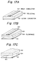
- Figs. 17A to 17C are diagrams showing a conventional high frequency transmission lines, in which Fig. 17A shows a microstrip line, Fig. 17B a suspended microstrip line, and Fig. 17C an inverted microstrip line. Those are used as high frequency signal transmission lines on circuit boards or as parts in delay lines.
- reference numeral 100 denotes an outer conductor, 102 a dielectric, 103 an inner conductor, and 104 a clearance.
- microstrip lines shown in Figs. 17A to 17C, have been used for the high frequency transmission lines.
- the microstrip line structured as shown in Fig. 17A is generally most extensively used.
- This microstrip line has an inner conductor (conductor used as a signal line) 103 provided on one side of a dielectric 102, and an outer conductor (conductor normally used as GND electrode) 101 provided on the other side (side opposite the inner conductor 103) of the dielectric 102.
- this microstrip line structured as described is widely used is because it is smaller and less expensive and easier to manufacture than other microwave circuits such as wave guide circuits when it is used in forming a flat high frequency circuit, for example.
- microstrip line mentioned above notably suffers general losses in the transmission line (e.g. radiation loss, dielectric loss, and conductor loss).
- improved products have been developed, which include the suspended microstrip line shown in Fig. 17B and the inverted microstrip line shown in Fig. 17C.
- the suspended microstrip line as depicted in Fig. 17B, has the inner conductor and dielectric suspended by a support member to provide a clearance 104 between the dielectric 102 and the outer conductor 101.
- the inverted microstrip line has the inner conductor 103 provided on one side of the dielectric 102, which side faces the outer conductor 101 and provides a clearance 104 between the dielectric 102 and the outer conductor 101 as shown in Fig. 17C.
- Figs. 18A and 18B show examples of high frequency filters
- Figs. 19A to 19C show equivalent circuits of the high frequency filter of Figs. 18A and 18B.
- reference numeral 111 denotes a substrate (dielectric), 112 and 113 ⁇ /4 type strip resonators, 114 a coupling capacitor, 115 through-holes, 116 GND electrodes (wide-area-contact grounding metals), 117 and 118 ⁇ /4 type dielectric resonators, IN input terminals, OUT output terminals, C1 to C4 capacitors, and L1 to L3 coils.
- Figs. 18A and 18B show Various types of high frequency filters. Out of them, band pass filters will be described with reference to Figs. 18A and 18B, in which Fig. 18A shows a strip line filter, and Fig. 18B shows a dielectric filter.
- two ⁇ /4 type strip resonators 112 and 113 are provided a certain distance apart from each other on one side of the substrate 111 (dielectric) 111, a coupling capacitor 114 is connected between those resonators, and a GND electrode (wide-area-contact grounding metal) 116 is formed on the other side of the substrate 111.
- a through-hole 115 is provided at the end of each of the two ⁇ /4 type strip resonators 112 and 113.
- the dielectric filter is structured as shown in Fig. 18B. More specifically, two ⁇ /4 type dielectric resonators 117 and 118 are arranged side by side and covered respectively with a GND electrode (wide-area-contact grounding metal), and a coupling capacitor 114 is placed in the middle to connect those dielectric resonators 117 and 118.
- GND electrode wide-area-contact grounding metal
- the two ⁇ /4 type dielectric resonators 117 and 118 are coaxial type dielectric resonators which each include a conductor and are covered over their circumferential surface with a GND electrode 116.
- FIG. 19A An equivalent circuit of the high frequency filter (band pass filter) as mentioned above is shown in Fig. 19A.
- the ⁇ /4 type strip resonators 112 and 113, and the ⁇ /4 type dielectric resonators 117 and 118 in Figs. 18A and 18B are equivalent to a parallel resonance circuit with L1 and C1 and a parallel resonance circuit with L2 and C2, respectively.
- the high frequency filters such as these are sometimes added with a coil or capacitors.
- Equivalent circuits of the high frequency filters with the additional coil and capacitors may be as shown in Figs. 19B and 19C, respectively (e.g., a polarized band pass filter, and a band rejection filter).
- Fig. 19B is an example in which a coil L3 is connected in parallel with the coupling capacitor 114.
- Fig. 19C is an example in which capacitors C3 and C4 are added to the circuit in Fig. 19A.
- Dielectric resonator (refer to Figs. 20A and 20B)
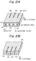
- Figs. 20A and 20B show a prior-art dielectric resonator ( ⁇ /4 type), in which Fig. 20A is a perspective view and Fig. 20B is a sectional view taken along the line X-Y.
- reference numeral 121 denotes a dielectric resonator, 122 a dielectric, 123, a through-hole, 124 a resonant conductor, and 125 a GND electrode.
- the prismatic and columnar dielectric resonators have been known. Out of these two types, a prismatic one is shown in Figs. 20A and 20B. As shown in the figures, the dielectric resonator 121 has the through-hole 123 formed in the center in the longitudinal direction of the dielectric 122. The GND electrode 125 is formed by covering the all sides of the dielectric 122, except for one of two sides having an opening of the through-hole 123 with a conductor.
- the internal circumferential surface of the through-hole 123 is covered with a resonant conductor 124, one end of which is integral with the GND electrode 125.
- the other end of the resonant conductor 124 which is not integral the GND electrode 125 is so formed as to be used for connection with an external terminal (not shown).
- the prior-art dielectric resonator has problems enumerated below.
- Dielectric filter (refer to Figs. 21A and 21B)
- Fig. 21A and 21B show a prior-art dielectric filter, in which Fig. 21A is a perspective view taken from the top side, while Fig. 21B is a perspective view taken from the reverse side.
- This dielectric filter is a kind of the band pass filter, and includes a plurality of 1/4 wavelength resonant conductors.
- the above-mentioned resonant conductors constitute resonators, respectively.
- a dielectric filter 121 comprises a dielectric 122, a plurality of through-holes 123, resonant conductors 124 covering the internal circumferential surfaces of the through-holes 123, and a GND electrode 125 covering the whole external circumferential surfaces of the dielectric 122 except for one side of the dielectric 122 (the side where there is the resonant conductors 124).
- the dielectric 122 has slots 126 formed therein. By those slots 126, the resonant conductors 124 are separated and the coupling among the resonant conductors 124 is adjusted.
- the GND electrode 125 is provided also on the internal surfaces of the slots 126. On the side where the slots 126 are provided, the resonant conductors 124 and the GND electrode 125 are connected (GND side ends of resonant conductors 124 are commonly connected with each other).
- the said plurality of resonant conductors 124 (four resonant conductors in this case) have different lengths (some resonant conductors may have the same length) so as to have different resonance frequencies with each other.
- Such dielectric filter 122 is made in a manner described below, for example. First of all, a dielectric 122 is produced with through-holes 123 and slots 126 provided by press forming. Then, all sides (including the internal surfaces of the through-holes 123) except for one side where there exist the through-holes 123 are metallized.
- the conductor formed inside the through-holes 123 is used as the resonant conductors 124, and the conductor formed on the external circumferential surface of the dielectric 122 is used as the GND electrode 125.
- the prior-art dielectric resonator has problems enumerated below.
- the line impedance of the resonator decreases, so that the Q of the resonator decreases, too.
- the resonator must be made thicker in the through-thickness direction for greater ⁇ to prevent the input impedance from decreasing.
- VCO Voltage Control Oscillator
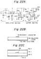
- Figs. 22A to 22C show explanatory diagrams of the prior-art example, in which Fig. 22A is a circuit example of the VCO (voltage control oscillator), Fig. 22B is an explanatory diagram of the microstrip line, and Fig. 22C is an explanatory diagram of the tri-plate type strip line.
- VCO voltage control oscillator
- Fig. 22B is an explanatory diagram of the microstrip line
- Fig. 22C is an explanatory diagram of the tri-plate type strip line.
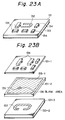
- Figs. 23A and 23B show two examples of prior-art VCO modules.
- Fig. 23A is a perspective view of first example of the VCO module
- Fig. 23B is an exploded view in perspective of second example of the VCO module.
- R11 to R18 denote resistors
- C11 to C21 denote capacitors
- L11 and L12 denote coils
- CV denotes a varactor diode (variable capacitance diode)
- SL denotes a strip line
- CT denotes a control voltage input terminal
- OUT denotes an output terminal
- Vcc denotes a power supply
- Tr1 and Tr2 denote transistors.
- Reference numerals 131 and 131-1 to 131-3 denote dielectric layers, 132 denotes a resonant conductor, 133 and 133-1 to 133-2 denote GND electrodes, 134 denotes parts (discrete parts), 135 denotes a through-hole, and 136 denotes a blank area.
- VCO Voltage Control Oscillator
- This VCO comprises an oscillator section and a buffer section, which are coupled through the coupling capacitor C17.
- the oscillator section includes the transistor Tr1, the strip line SL, the varactor diode (variable capacitance diode) CV, the capacitors C11 to C16, the resistors R11 to R14, and the coil L11.
- the buffer section includes the transistor Tr2, the capacitors C18 to C21, the resistors R15 to R18, and the coil L12.
- the oscillator When a control voltage is applied to the control voltage input terminal of the oscillator, the oscillator oscillates at a frequency corresponding to the control voltage, and supplies an output signal of the VCO from the output terminal OUT.
- strip line SL constitutes a resonator (strip line resonator), and how it is mounted on the substrate is shown by examples in Figs. 22B and 22C.
- Fig. 22B shows as an example of a microstrip line made by forming a resonant conductor 132 on the front surface of the dielectric layer 131 constituting the substrate, and forming a GND pattern on the back side thereof.
- Fig. 22C shows as an example a tri-plate type strip line which contains the resonant conductor 132 in a multi-layer substrate, and which is sandwiched by the GND patterns 133-1 and 133-2.
- Fig. 23A shows the first example of VCO module including a microstrip line formed as depicted in Fig. 22B.
- This VCO module has the resonant conductor 132 (thick film printing) formed on the front surface of the dielectric layer 131 constituting the substrate (a single substrate or a multi-layer substrate) and parts 134 (discrete parts) such as transistors and resistors mounted thereon.
- the GND pattern 133 is formed on the back surface of the above-mentioned dielectric layer 131.
- Fig. 23B shows the second example of VCO module including a strip line formed as depicted in Fig. 22C.
- This module has parts 134 (discrete parts) such as transistors and resistors mounted on the first dielectric layer 131-1 constituting a multi-layer substrate, and the GND pattern 133-1 formed on the second dielectric layer 131-2, the resonant conductor 132 on the third dielectric layer 131-3, and the GND pattern 133-2 formed on the back side of the third dielectric layer 131-3.
- the blank area 136 (an area devoid of a conductor) is provided in a part of the GND pattern 133-1, in the middle of which the through-hole electrode 135 is provided.
- the resonant conductor 132 and the parts 134 are connected through a blind through-hole (filled with a conductor) using the through-hole electrode 135 as a connection point.
- the resonant conductor is contained between the dielectric layers, it is expected that a wavelength is shortened to ⁇ / ⁇ ⁇ r ⁇ .
- the series resistance (r s ) can be decreased in proportion to the amount by which the resonant conductor is shortened, and therefore, the Q becomes high.
- the dielectric conductor is contained in the dielectric layers, it is difficult to adjust the resonator.
- the present invention has been made to solve the above problems, and has as its object to reduce in size a high frequency device by using a plurality of dielectric layers having different dielectric constants in combination, and thereby increasing the line impedance without decreasing Q.
- Q under unloaded (denoted as Qu) is defined by the following equation.
- 1 Qu 1 Qc + 1 Qd + 1 Qr (1)
- Qc denotes Q by a transmission line conductor
- Qd denotes Q by a dielectric
- Qr denotes Q by radiation.
- the wavelength shortening occurs which is expressed by the following formula and the resonant conductor length of a ⁇ /4 type resonator can be expressed by the formula ⁇ /4 ⁇ ⁇ r ⁇ .
- the resonant conductor (inner conductor) is pinched by high dielectric layers (dielectric layers with high dielectric constant) from both sides of the laminated direction, and no portion of the resonant conductor is exposed to the space as in the prior art, so that the resonant conductor length can be shortened to ⁇ /4 ⁇ ⁇ r ⁇ compared with the prior art.
- the presence of the low dielectric layers (dielectric layers with low dielectric constant) between the high dielectric layers and the GND electrode prevents the C component (capacitance component) from increasing even if the thickness of the dielectric resonator in the laminated direction is reduced. Therefore, a large line impedance Zo can be obtained.
- the wavelength shortening mentioned above permits the dielectric resonator to be shortened in the longitudinal direction.
- the series resistance component r s decreases, Qc increases, and also, Q under unloaded (Qu) increases.
- small-size high frequency devices can be produced without reducing the Q of the resonator.
- FIGs. 1A and 1B are diagrams showing a high frequency communication line according to a first embodiment of the present invention, in which Fig. 1A is a sectional view of the high frequency communication line, while Fig. 1B is an exploded view in perspective of a part (third and fourth dielectric layers) of Fig. 1A.
- reference numerals 1 to 4 denote first to fourth dielectric layers of a multi-layer substrate, respectively, 5 denotes an inner conductor, 6 and 7 denote GND electrodes, and 8 denotes blind through-holes (filled with a conductor).
- the first embodiment is a case in which a high frequency device according to the present invention is used as a high frequency transmission line in a signal communication line or a delay line.
- a multi-layer substrate is formed by laminating first to fourth dielectric layers 1 to 4.
- the first dielectric layer 1 and the fourth dielectric layer 4 are made of a material with a low dielectric constant ( ⁇ 2)
- the second dielectric layer 2 and the third dielectric layer 3 are made of a material with a high dielectric constant ( ⁇ 1, where ⁇ 1 > ⁇ 2).
- An inner conductor 5 used as a signal transmission line for propagating a high frequency signal is provided on the third dielectric (high dielectric constant) layer 3.
- An outer conductor (GND electrode) 6 for giving a ground potential (GND) is provided on the first dielectric (low dielectric constant) layer 1, and another outer conductor (GND electrode) 7 for also giving a ground potential (GND) is provided under the fourth dielectric (low dielectric constant) layer 4.
- the outer conductors 6 and 7 are connected to make them at the same potential (GND potential).
- high dielectric layers 2 and 3 are arranged on both sides of the inner conductor 5 in the laminating direction of the dielectric layers 1 to 4.
- Low dielectric layers 1 and 4 are arranged on both sides of the high dielectric layers 2 and 3, and on both sides of these low dielectric layers 1 and 4, outer conductors 6 and 7 are arranged, respectively. In this manner, a high frequency transmission line is formed.
- the high frequency communication line is formed in a tri-plate structure by having the inner conductor sandwiched by high dielectric layers, then sandwiched by low dielectric layers, and thereafter sandwiched by outer conductors.
- this high frequency transmission line is made in the same manner as by a method of manufacturing a ceramic multi-layer substrate, for example.
- a sheet with a relatively high dielectric constant is used for the second and third dielectric layers 2 and 3.
- a sheet with a relatively low dielectric constant is used for the first and fourth dielectric layers.
- the dielectric layers 1 to 4 made of those sheets are to be laminated to form a multi-layer substrate.
- the inner conductor 5 as the signal line is formed by printing a conductor paste on the third dielectric layer 3, and the outer conductors 6 and 7 (conductors for GND layer, for example) are formed on the outer surfaces of the first and fourth dielectric layers 1 and 4 by solidly printing a conductor paste (printing all over the whole surface).
- the high dielectric constant value ⁇ 1 should normally be 10 or larger, preferably 20 or larger, more preferably 30 or larger.
- the low dielectric constant value should normally be 20 or smaller, or more preferably 10 or smaller.
- dielectric materials used for the present invention dielectric materials of titanic acid family, for example, rutile family, may be used for the high dielectric constant ( ⁇ 1) material, while Al2O3, SiO2, forsterite, cordierite may be used for the low dielectric constant ( ⁇ 2) material.
- a combination of those material is selected to meet the condition ⁇ 1 > ⁇ 2. Above all, it is desirable to set a large difference between ⁇ 1 and ⁇ 2.
- the inner conductor 5 which serves as a transmission line for a high frequency signal, is formed in the longitudinal direction almost in the center of the surface of the third dielectric layer 3.
- the inner conductor 5 may have an optional width suitable for the impedance of the signal transmission line.
- this embodiment provides following effects.
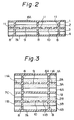
- Fig. 2 is a diagram showing a high frequency filter (in sectional view) according to a second embodiment.
- the same reference numerals as in Figs. 1A and 1B denote the same parts.
- Reference numeral 9 denotes a first resonant conductor, 10 a second resonant conductor, 11 conductors (GND electrode), and 6A and 7A GND electrodes.
- the two resonant conductors 9 and 10 (resonant conductors of the strip line resonator) corresponding in function to the inner conductor 5 mentioned above are mounted on the same dielectric layer 3, and the outer conductors 6A and 7A are used as GND electrodes, which are connected with a coupling capacitor to form a high frequency filter (band pass filter).
- the multi-layer substrate constituting the high frequency filter according to the second embodiment is formed by using the same dielectric layers as in these multi-layer substrate of the first embodiment.
- first and fourth dielectric layers 1 and 4 are formed by low dielectric layers (dielectric constant ⁇ 2), and the second and third dielectric layers 2 and 3 are formed by high dielectric layers (dielectric constant ⁇ 1, where ⁇ 1 > ⁇ 2).
- the first and second resonant conductors 9 and 10 are mounted on the third dielectric layer 3, and conductors 11 used as GND electrodes are provided a specified distance apart from each other and as if they surrounded the first and second resonant conductors 9 and 10.
- the first and second resonant conductors 9 and 10 constitute ⁇ /4 type strip resonators ( ⁇ is wavelength of high frequency signal), respectively, and they are at one end connected to the above-mentioned conductors 11.
- the GND electrodes 6A and 7A are provided on the upper side (outside surface) of the first dielectric layer 1 and on the under side (outside surface) of the fourth dielectric layer 4, and are connected through blind through-holes (filled with a conductor) 8 with the conductors 11, to be used at the same potential.
- the first and second resonant conductors 9 and 10 are connected with each other via a capacitor (not shown) contained in the multi-layer substrate.
- the capacitor and the resonant conductors constitute a strip line filter.
- Fig. 3 is a diagram showing a high frequency filter (sectional view) according to a third embodiment.
- the same reference numerals as these in Figs. 1A to 2 denote the same parts.
- reference numerals 7C, 11A, and 11B denote GND electrodes, and 1A, 2A, 3A, 4A, 1B, 2B, 3B, and 4B denote first to eighth dielectric layers.
- This third embodiment is a modification of the second embodiment.
- the first and second resonant conductors 9 and 10 are arranged in the laminating direction.
- the second, third, sixth and seventh dielectric layers 2A, 3A, 2B, and 3B are all formed of a high dielectric constant material (dielectric constant ⁇ 1), and the first, fourth, fifth, and eighth dielectric layers 1A, 4A, 1B, and 4B formed of a low dielectric constant material (dielectric constant ⁇ 2) are provided between those high dielectric layers and the GND electrodes 6A, 7C, and 7A.
- the first and second resonant conductors 9 and 10 are respectively placed between the high dielectric layers 2A and 3A, and 2B and 3B.
- the high dielectric layers are surrounded by low dielectric layers.
- the second and third embodiments offer following effects.
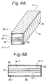
- Figs. 4A and 4B are diagrams showing a dielectric resonator according to a fourth embodiment, in which Fig. 4A is a perspective view of the dielectric resonator and Fig. 4B is a sectional view taken along the line X-Y of Fig. 4A.
- reference numeral 31 denotes a dielectric resonator, 34 a resonant conductor, 35 a GND electrode, 36-1 and 36-2 low dielectric layers, and 37-1 and 37-2 high dielectric layers.
- the fourth embodiment is a dielectric resonator constituted by using the resonant conductor 34 corresponding to the aforementioned inner conductor 5, and the peripheral GND electrode 35 as an outer conductor.
- this dielectric resonator 31 is prismatic in external appearance, and has the resonant conductor 34 placed in the center along the longitudinal direction.
- the high dielectric layers 37-1 and 37-2 are provided only around the resonant conductor 34.
- the low dielectric layers 36-1 and 36-2 are provided between the high dielectric layer 37-1 and the outside GND electrode 35 and between the high dielectric layer 37-2 and the outside GND electrode 35.
- the high dielectric layers 37-1 and 37-2 should preferably be thinner than the low dielectric layers 36-1 and 36-2.
- this dielectric resonator 31 is made by using laminating technology used for the multi-layer substrate, and therefore, does not have a through-hole present in the prior art.
- the dielectric resonator 31 is made in the manner described below, for example. First, a low dielectric layer 36-1 is formed, on which a high dielectric layer 37-1 is laminated.
- a conductor is printed to form the resonant conductor (thick film pattern) 34.
- a high dielectric layer 37-2 is laminated, so that the resonant conductor 34 is surrounded at the top, bottom, left and right sides with the high dielectric layers 37-1 and 37-2.
- the width of the resonant conductor 34 is made narrower than the high dielectric layers 37-1 and 37-2.
- a low dielectric layer 36-2 is laminated on the above-mentioned high dielectric layer 37-2, thereby making the whole laminated body prismatic.
- a GND electrode 35 is formed on all sides of the dielectric resonator except for one of two sides where the resonant conductor 34 is exposed. This GND electrode 35 is formed by printing a conductor paste, for example. At this step, the resonant conductor 34 is formed so that one end thereof contacts to the GND electrode 35, as shown in Fig. 4B.
- each of the above-mentioned low dielectric layers 36-1 and 36-2 is not limited to one layer, but may be any optional number of layers (multiple layers). Also, each of the high dielectric layers 37-1 and 37-2 may be formed in multiple layers.
- the low dielectric layer should preferably be thicker than the high dielectric layer.
- Figs. 5A and 5B are diagrams showing a dielectric resonator according to a fifth embodiment, in which Fig. 5A is a perspective view of the dielectric resonator, while Fig. 5B is a sectional view taken along the line X-Y of Fig. 5A.
- the same reference numerals as in Figs. 4A and 4B denote the same parts.
- Reference numerals 34-1 and 34-2 denote resonant conductors, and 37-1 to 37-3 denote high dielectric layers.
- the fifth embodiment was made to reduce the loss of the resonant conductor by using two resonant conductors, and its structure is shown in Figs. 5A and 5B. Also in this embodiment, the high dielectric layers are disposed only around the resonant conductors.
- the dielectric resonator 31 is made in the manner as described below, for example. First, a high dielectric layer 37-1 is laminated on a low dielectric layer 36-1, and then a resonant conductor 34-1 is formed (in thick film pattern) on the high dielectric layer 37-1. Thereafter, a high dielectric layer 37-2 is laminated thereon.
- the resonant conductor 34-2 is formed (in thick film pattern) on the high dielectric layer 37-2, and on which a high dielectric layer 37-3 is laminated. Thereafter, a low dielectric layer 36-2 is laminated on the layer 37-3. The whole laminated body is formed in a prismatic shape. Finally, a GND electrode 35 is formed on all external sides of the laminated body except for one of two sides where the resonant conductors 34-1 and 34-2 are exposed, and this GND electrode 35 is connected to one end of each of the resonant conductors 34-1 and 34-2.
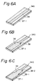
- Figs. 6A to 6F show structural examples of the resonant conductors in the above-mentioned fourth and fifth embodiments.
- the same reference numerals as in Figs. 4A to 5B denote the same parts.
- Reference numeral 34G denotes the GND terminals, and 38, 38-1 and 38-2 denote the point where the width changes.
- the resonant conductor 34 is formed as a thick film pattern on the high dielectric layer 37-1.
- the thick film pattern may be formed in various forms as shown in examples 1 to 6.
- the resonant conductor is denoted by reference numeral 34, and the high dielectric layer by 37-1.
- the above-mentioned patterning is applied to the resonant conductors 34-1 and 34-2, and the high dielectric layer 37-2 in the fifth embodiment.
- Example 1 in Fig. 6A is a thick film pattern of the resonant conductor 34 in the form of a strip with a fixed width.
- Example 2 in Fig. 6B is a thick film pattern which has a change point 38 of the width in almost the middle of the longitudinal direction of the resonant conductor 34.
- the thick film pattern width is narrow, and for the other range, the width is made wider (the width changes in two stages).
- Example 3 in Fig. 6C is a resonant conductor 34 having two width change points 38-1 and 38-2 at which the resonant conductor 34 is divided into three portions with almost equal lengths in the longitudinal direction.
- the pattern width is widest, for the range between the width change points 38-1 and 38-2, the pattern width is intermediate, and for the range from the width change point 38-2 to the GND-side end 34G, the pattern width is narrowest.
- the thick film pattern of the resonant conductor 34 is varied in three stages.
- Example 4 in Fig. 6D is a resonant conductor having the width change point 38 near the end thereof with the width wide near that end and narrow from the width change point 38 to the GND-side end 34G.
- the reason for providing the width change points is to prevent a harmful resonance in higher modes (harmonic suppress measure).
- Example 5 in Fig. 6E is a resonant conductor 34 formed by a thick film pattern having a fixed width but meandering. This meandering provides the resonant conductor with a substantially long length, so that the dielectric resonator can be made short in longitudinal length and hence, small in size.
- Example 6 in Fig. 6F is a resonant conductor 34 formed by a tapered thick film pattern. As illustrated, the thick film pattern is tapered so that the width is narrowest at the GND-side end 34G and widest at the opposite end.
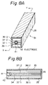
- Figs. 7A and 7B, Figs. 8A and 8B, and Figs. 9A and 9B show structural examples of the electrodes (for external terminals) in the four and fifth embodiment mentioned above.
- the same reference numerals as in Figs. 4A to 6B denote the same parts.
- Reference numerals 40, 42, and 43 denote electrodes, and 44 denotes blank areas.
- the dielectric resonator 31 shown in the fourth and fifth embodiments mentioned above need to be fitted with electrodes for external terminals, as shown in Figs. 7A and 7B, Figs. 8A and 8B, and Figs. 9A and 9B, for example.
- Fig. 7A is a perspective view of the dielectric resonator
- Fig. 7B is a sectional view taken along the line X-Y of Fig. 7A.
- Example 1 in Figs. 7A and 7B is a structural example of the dielectric resonator in which a chip-like electrode 40 is mounted almost in the center of the side devoid of the GND electrode 35, connected to the resonant conductor 34.
- This electrode 40 is used as a terminal for connection with an external circuit.
- Example 2 in Figs. 8A and 8B is a structural example of the dielectric resonator 31 in which a shallow pit (blind hole) 41 is provided almost in the center of the side without the GND electrode 35, at the internal circumference of which pit 41 an electrode 42 is formed, and the electrode 42 is connected to the resonant conductor 34.
- a shallow pit (blind hole) 41 is provided almost in the center of the side without the GND electrode 35, at the internal circumference of which pit 41 an electrode 42 is formed, and the electrode 42 is connected to the resonant conductor 34.
- the pit 41 is formed, and then, the conductor of the electrode 42 is attached.
- a convex electrode, insertable into the electrode 42 is inserted for connection with an external circuit.
- the electrode 42 serving as a female connector is connected detachably to an external electrode (male connector, in this case).
- Example 3 in Figs. 9A and 9B is a structural example made in SMD (surface mounted device) application. As illustrated, a rectangular electrode 43 is mounted at the side devoid of the GND electrode 35, and is connected with the internal resonant conductor 34.
- the electrode 43 is to have an electrode width corresponding to a length from the bottom of the low dielectric layer 36-1 to the top of the low dielectric layer 36-2.
- blank areas 44 are provided at the peripheral the electrode 43 (at the top side and bottom side).
- the fourth and fifth embodiments provide following effects.
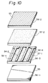
- Fig. 10 and Figs. 11A to 11B are diagrams showing a sixth embodiment, in which Fig. 10 is an exploded view in perspective of a dielectric filter, while Figs. 11A and 11B are perspective views of a dielectric filter (Fig. 11A is a view taken from the front side, and Fig. 11B is a view taken from the back side).
- reference numeral 54-1 to 54-4 denote ⁇ /4 type resonant conductors
- 55 denotes a GND electrode
- 56-1 and 56-2 denote low dielectric layers
- 57-1 and 57-2 denote high dielectric layers
- 58 denotes an input terminal
- 59 denotes an output terminal
- 60 denotes blank areas.
- the dielectric filter (band pass filter) in the sixth embodiment has four resonant conductors.
- the high dielectric layer (dielectric constant ⁇ 1) 57-1 is laminated on the low dielectric layer (dielectric constant ⁇ 2) 56-1.
- the relation ⁇ 1 > ⁇ 2 holds.
- the four resonant conductors 54-1, 54-2, 54-3, and 54-4 are arranged specified distances apart from one another on the mentioned high dielectric layer 57-1. Those resonant conductors 54-1 to 54-4 differ in length, and therefore, differ in the resonance frequency, too.
- each of the resonant conductors 54-1 to 54-4 (the ends where those conductors are wide in Fig. 10) is on the GND side, and the opposite ends thereof are on the signal input side.
- the high dielectric layer (dielectric constant ⁇ 1) 57-2 is laminated, so that the resonant conductors 54-1 to 54-4 are sandwiched by the high dielectric layers 57-1 and 57-2.
- the low dielectric layer (dielectric constant ⁇ 2) 56-2 is laminated.
- GND electrodes 55 are provided both on the upper side of the low dielectric layer 56-2 and on the under side of the low dielectric layer 56-1.
- the dielectric filter is constituted in such a structure that the resonant conductors 54-1 to 54-4 are sandwiched by the high dielectric layers 57-1 and 57-2 (on both sides of the laminated direction), and the layers 57-1 and 57-2 are further sandwiched by the low dielectric layers 56-1 and 56-2.
- the all sides of the laminated body, except for one side used as a signal input side, are covered with the GND electrode 55, and the signal input side is provided with the input terminal (IN) 58 and the output terminal (OUT) 59.
- the input terminal 58 and the output terminal 59 are made of a conductor with a length substantially equal to the thickness of the laminated body, so that part of the GND electrode 55 surrounding those terminals are cut off to form the blank areas (areas without any conductor) 60. If the dielectric filter is structured as described, the input terminal 58 and the output terminal 59 can be prevented from contacting the GND electrode 55. By providing these terminals, the dielectric filter can be made ready for SMD (Surface Mounted Device) application.
- SMD Surface Mounted Device
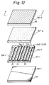
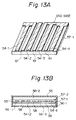
- Fig. 12 and Figs. 13A and 13B show a seventh embodiment, in which Fig. 12 is an exploded view in perspective of a dielectric filter, and Figs. 13A and 13B are structural diagrams of the dielectric filter (Fig. 13A is a partially enlarged view, and Fig. 13B a sectional view taken along the line X-Y of Fig. 13A).
- Fig. 13A is a partially enlarged view
- Fig. 13B a sectional view taken along the line X-Y of Fig. 13A.
- Reference numeral 61 denotes low dielectric parts.
- This seventh embodiment is a case in which low dielectric parts are placed between a plurality of resonant conductors so as to adjust the degree of coupling between the resonators.
- a high dielectric layer (dielectric constant ⁇ 1) 57-1 is laminated, and on this high dielectric layer 57-1, four resonant conductors 54-1, 54-2, 54-3, and 54-4 are formed.
- Low dielectric members (dielectric constant ⁇ 2) 61 are formed in respective spaces between the resonant conductors 54-1 to 54-4, by printing or sticking them in sheet form.
- a high dielectric layer (dielectric constant ⁇ 1) 57-2 is laminated, and on which in turn a low dielectric layer 56-2 (dielectric constant ⁇ 2) is laminated.
- a GND electrode 55 is provided on the under side of the low dielectric layer 56-1 and on the upper side of the low dielectric layer 56-2.
- the GND electrode 55 is also attached to the whole circumferential surface of the thus formed laminated body except for one side (the input side of the resonant conductor).
- the degree of coupling between the resonators is adjusted by varying the shape of the low dielectric parts 61 provided between each of the resonant conductors.
- step 1 to step 7 a dielectric filter is completed.
- the GND electrode as the outermost layer may be formed in the step 6.
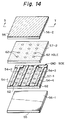
- Fig. 14 is an exploded view in perspective of a dielectric filter according to an eight embodiment.
- Figs. 15A and 15B are structural diagrams of the dielectric filter according to the eighth embodiment, in which Fig. 15A is a perspective view of a high dielectric layer, while Fig. 15B is a sectional view taken along the line S-T in Fig. 14.
- the same reference numerals as in Figs. 10 to 13B denote the same parts.
- Reference numeral 62 denotes through-holes.
- the eighth embodiment is a case in which a plurality of holes are opened in the high dielectric layers, and the holes are filled with a low dielectric substance so that the low dielectric substance lie between the resonant conductors to thereby adjust the degree of coupling between the resonators.
- a low dielectric layer 56-1, high dielectric layers 57-1 and 57-2, and a low dielectric layer 56-2 are laminated as illustrated.
- the arrangement of the dielectric layers and the structure of resonant conductors 54-1 to 54-4, and a GND electrode 55 are the same as that in the sixth embodiment.
- the through-holes are opened by punching the high dielectric layers 57-1 and 57-2, and the through-holes are filled with a low dielectric substance.
- the holes 62 opened in the high dielectric layers 57-1 and 57-2 are positioned so that they are arranged between the resonant conductors 54-1 to 54-4 when the layers are laminated.
- the dielectric constant of the low dielectric substance filled in the holes 62 is to be ⁇ 2 ( ⁇ 1 > ⁇ 2) as in the low dielectric layers 56-1 and 56-2, for example.
- step 1 to step 7 a dielectric filter is completed.
- the degree of coupling between the resonators is adjusted by the size and the number of the holes 62.
- the low dielectric parts which are formed by being filled in the holes 62 on the high dielectric layer 57-1 in Fig. 14, may be filled in the holes 62 simultaneously with forming (by printing or the like) of the low dielectric strips 61 arranged between the resonant conductors as shown in Fig. 13A.
- the sixth to eighth embodiments can be modified as described below.
- the sixth to eighth embodiments offers the following effects.
- Fig. 16 is a sectional view of the voltage control oscillator (VCO) in a ninth embodiment.
- VCO voltage control oscillator
- reference numerals 71-1L to 71-3L, and 71-6L and 71-7L denote low dielectric layers
- 71-4H and 71-5H denote high dielectric layers
- 73-1A and 73-2 denote GND electrodes
- 72 denotes resonant conductor (strip line resonator)
- 79 denotes a blank area (without conductor)
- 80 denotes side-face electrode.
- the ninth embodiment is a voltage control oscillator (VCO) formed by using a resonant conductor (strip line resonator) corresponding to the inner conductor in the first embodiment and connecting other parts thereto.
- VCO voltage control oscillator
- a resonator is mounted in the substrate on which discrete parts are mounted, and in order to obtain a thin substrate, a structure described below is used.
- a multi-layer substrate is formed by the first to seventh dielectric layers 71-1L, 71-2L, 71-3L, 71-4H, 71-5H, 71-6L, and 71-7L.
- the voltage control oscillator is composed of an oscillator section and a buffer section.
- This buffer section serves to protect the oscillator against adverse effects from voltage fluctuation and so on the output side of the VCO.
- transistors and other discrete parts are mounted on the first dielectric layer (low dielectric) 71-1L of the multi-layer substrate, while a coil and a wiring pattern are formed on the second dielectric layer (low dielectric) 71-2L (by solid printing).
- the GND pattern 73-1A is formed (by solid printing) on the whole surface, except for the blank area (area without conductor) 79, of the third dielectric layer (low dielectric layer) 71-3L.
- the resonant conductor 72 is formed (by printing a conductor paste) on the fifth dielectric layer (high dielectric layer) 71-5H.
- the GND pattern (wide-area-contact GND pattern) 73-2 is formed (in solid printing) on the seventh dielectric layer 71-7L.
- the above-mentioned patterns are extended by conductor patterns to the end of the dielectric layers, and connected to the GND electrode 80 formed on the GND side face for SMD (Surface Mounted Device) application.
- SMD Surface Mounted Device
- the GND pattern 73-1A may be constituted so as to cover the resonant conductor 72.
- the low dielectric layers 71-3L and 71-6L it is desirable to form the blank area 79 as shown in Fig. 16.
- the above-mentioned blank area 79 is made to have substantially the same shape as the resonant conductor 72 (somewhat larger than this), and formed above the resonant conductor 72.
- the GND pattern 73-1A is prevented from being present above (in the laminated direction) the resonant conductor 72.
- the GND pattern 73-1A is formed by patterning on the low dielectric layer 71-3L with the blank area 79 left as blank.
- the resonant conductor In an oscillator, the resonant conductor is used as a mere inductive element, and hence, there is no problem of radiation loss. Therefore, the resonant conductor need not be mounted in a tri-plate structure.
- One end, in the GND side, of the resonant conductor 72 is extended to the end of the fifth dielectric layer 71-5H and connected to the GND electrode 80 (not illustrated as it is in Fig. 16), while the other end is connected to a capacitor (a discrete part in this case) mounted on the surface of the substrate, for example.
- the strip line resonator is structured such that the GND pattern 73-2 is formed under the resonant conductor 72 with interposition of a dielectric layer, whereas no GND pattern is formed but only dielectric layers are formed above the resonant conductor 72. Also, this resonator is disposed at peripheral (including under side ) of a transistor of the oscillator section mounted on the surface of the substrate.
- the resonant conductor 72 of the strip line resonator is placed between the high dielectric layers 71-4H and 71-5H, thereby shortening the wavelength. Consequently, a resonator with high Q can be obtained, and the oscillator section, particularly the strip line resonator, is protected against adverse effects from the buffer section.
- the strip line resonator can be adjusted as follows.
- a trimming GND pattern (not shown) is formed on the low dielectric layer 71-1L just above a part of the strip line resonator 72, which part is not connected to the GND electrode 80, and connected to the GND electrode 73-1A. Then, the trimming GND pattern is trimmed. Since when trimming, a capacitance component between the resonant conductor 72 and the trimming GND pattern is varied, the resonance frequency of the strip line resonator can be adjusted.
- the ninth embodiment offers the following effects.
- High frequency devices can be applied to high frequency transmission lines such as a high frequency signal line or a delay line, high frequency filters, high frequency oscillators, and resonators, and other devices.
Abstract

Description
- The present invention relates to a high frequency device, such as a high frequency resonator, a high frequency filter, a high frequency oscillator, and a dielectric resonator, used in radio equipment or other communication equipments.
- Various types of high frequency devices have been conventionally used in wireless equipment including portable or cordless telephones, or other communication equipments.
- These high frequency devices include a high frequency filter, high frequency oscillator, dielectric resonator, high frequency amplifier, or duplexer.
- Hereinafter, examples of the conventional high frequency devices will be described with reference to the accompanying drawings.
- Figs. 17A to 17C are diagrams showing a conventional high frequency transmission lines, in which Fig. 17A shows a microstrip line, Fig. 17B a suspended microstrip line, and Fig. 17C an inverted microstrip line. Those are used as high frequency signal transmission lines on circuit boards or as parts in delay lines.
- In Figs. 17A to 17C, reference numeral 100 denotes an outer conductor, 102 a dielectric, 103 an inner conductor, and 104 a clearance.
- Conventionally, microstrip lines, shown in Figs. 17A to 17C, have been used for the high frequency transmission lines. Among them, the microstrip line structured as shown in Fig. 17A is generally most extensively used.
- This microstrip line has an inner conductor (conductor used as a signal line) 103 provided on one side of a dielectric 102, and an outer conductor (conductor normally used as GND electrode) 101 provided on the other side (side opposite the inner conductor 103) of the dielectric 102.
- The reason why this microstrip line structured as described is widely used is because it is smaller and less expensive and easier to manufacture than other microwave circuits such as wave guide circuits when it is used in forming a flat high frequency circuit, for example.
- However, the microstrip line mentioned above notably suffers general losses in the transmission line (e.g. radiation loss, dielectric loss, and conductor loss). In order to reduce the losses, improved products have been developed, which include the suspended microstrip line shown in Fig. 17B and the inverted microstrip line shown in Fig. 17C.
- The suspended microstrip line, as depicted in Fig. 17B, has the inner conductor and dielectric suspended by a support member to provide a
clearance 104 between the dielectric 102 and theouter conductor 101. - The inverted microstrip line has the
inner conductor 103 provided on one side of the dielectric 102, which side faces theouter conductor 101 and provides aclearance 104 between the dielectric 102 and theouter conductor 101 as shown in Fig. 17C. - The prior-art microstrip lines have problems described in the following.
- (1) In contrast to the ordinary microstrip line, the suspended microstrip line or inverted microstrip line is a transmission line with reduced loss, but it is necessary to form the inner conductor as a signal line by patterning on the dielectric and have the inner conductor overhang separated from the outer conductor which is GND conductor. Therefore, its setting is unstable and its manufacture is difficult.
- (2) The suspended microstrip line and the inverted microstrip line, for the structural reason, need to have the outer conductor (GND conductor) more than a certain extent wider than the width of the inner conductor (signal line). This makes it difficult to miniaturize the line.
- Figs. 18A and 18B show examples of high frequency filters, and Figs. 19A to 19C show equivalent circuits of the high frequency filter of Figs. 18A and 18B.
- In Figs. 18A and 18B and Figs. 19A to 19C,
reference numeral 111 denotes a substrate (dielectric), 112 and 113 λ/4 type strip resonators, 114 a coupling capacitor, 115 through-holes, 116 GND electrodes (wide-area-contact grounding metals), 117 and 118 λ/4 type dielectric resonators, IN input terminals, OUT output terminals, C1 to C4 capacitors, and L1 to L3 coils. - Various types of high frequency filters have been known. Out of them, band pass filters will be described with reference to Figs. 18A and 18B, in which Fig. 18A shows a strip line filter, and Fig. 18B shows a dielectric filter.
- As shown in Fig. 18A, two λ/4
type strip resonators coupling capacitor 114 is connected between those resonators, and a GND electrode (wide-area-contact grounding metal) 116 is formed on the other side of thesubstrate 111. At the end of each of the two λ/4type strip resonators hole 115 to connect theresonator 112 to theGND electrode 116. - The dielectric filter is structured as shown in Fig. 18B. More specifically, two λ/4 type
dielectric resonators coupling capacitor 114 is placed in the middle to connect thosedielectric resonators - The two λ/4 type
dielectric resonators GND electrode 116. - An equivalent circuit of the high frequency filter (band pass filter) as mentioned above is shown in Fig. 19A. As depicted in Fig. 19A, the λ/4
type strip resonators dielectric resonators - The high frequency filters such as these are sometimes added with a coil or capacitors. Equivalent circuits of the high frequency filters with the additional coil and capacitors may be as shown in Figs. 19B and 19C, respectively (e.g., a polarized band pass filter, and a band rejection filter).
- Fig. 19B is an example in which a coil L3 is connected in parallel with the
coupling capacitor 114. Fig. 19C is an example in which capacitors C3 and C4 are added to the circuit in Fig. 19A. - The prior-art high frequency filters as mentioned above have problems listed below.
- (1) In the case of the strip line filter as shown in Fig. 18A, the λ/4 type strip resonators used as signal line suffer a great radiation loss.
Since it is necessary to provide some distance between the λ/4 type strip resonators to prevent mutual interference, the width of the filter, above all else, has to be wide. - (2) In the case of a dielectric filter shown in Fig. 18B, the volume is large, so that a vexing problem is its occupied space in the whole volume of equipment in which it is mounted (particularly with mobile radio equipment).
- (3) The high frequency filters shown in Figs. 18A and 18B have resonators in two stages. In practice, high frequency filters are structured in many more stages, and therefore, invariably become large-sized filters. This makes it difficult to meet the general requirement for miniaturization of devices.
- (4) When the high frequency filters shown in Figs. 18A and 18B are added with a coil or capacitors as shown in Fig. 19B or 19C, the high frequency filters become large-sized filter blocks.
-
- Figs. 20A and 20B show a prior-art dielectric resonator (λ/4 type), in which Fig. 20A is a perspective view and Fig. 20B is a sectional view taken along the line X-Y.
- In Figs. 20A and 20B,
reference numeral 121 denotes a dielectric resonator, 122 a dielectric, 123, a through-hole, 124 a resonant conductor, and 125 a GND electrode. - As for the external appearance, the prismatic and columnar dielectric resonators have been known. Out of these two types, a prismatic one is shown in Figs. 20A and 20B. As shown in the figures, the
dielectric resonator 121 has the through-hole 123 formed in the center in the longitudinal direction of the dielectric 122. TheGND electrode 125 is formed by covering the all sides of the dielectric 122, except for one of two sides having an opening of the through-hole 123 with a conductor. - The internal circumferential surface of the through-
hole 123 is covered with aresonant conductor 124, one end of which is integral with theGND electrode 125. The other end of theresonant conductor 124 which is not integral theGND electrode 125 is so formed as to be used for connection with an external terminal (not shown). - The prior-art dielectric resonator has problems enumerated below.
- (1) This dielectric resonator is made in a small size by using a dielectric with high dielectric constant which causes wavelength at the resonance frequency to be shortened. However, since the resonant conductors are on one side exposed to the space (internal space of the through-holes), the resonant conductor length is not shortened to λ/4√

- (2) As the dielectric constant ε, or the material constant of the dielectric becomes large, the C component (capacitance component) of the resonator becomes large for its structural reasons. Therefore, the line impedance of the resonator decreases, so that the Q of the resonator decreases. Therefore, the prism needs to be made thicker for greater ε. Hence, this is another point which makes miniaturization difficult. Also, it is difficult to make a resonator in small size with high Q.
- Fig. 21A and 21B show a prior-art dielectric filter, in which Fig. 21A is a perspective view taken from the top side, while Fig. 21B is a perspective view taken from the reverse side.
- In those figures, the same reference numerals as in Figs. 20A and 20B denote the same components.
Reference numeral 126 denotes slots. - An example of conventional dielectric filter is shown in Figs. 21A and 21B. This dielectric filter is a kind of the band pass filter, and includes a plurality of 1/4 wavelength resonant conductors. The above-mentioned resonant conductors constitute resonators, respectively.
- As illustrated, a
dielectric filter 121 comprises a dielectric 122, a plurality of through-holes 123,resonant conductors 124 covering the internal circumferential surfaces of the through-holes 123, and aGND electrode 125 covering the whole external circumferential surfaces of the dielectric 122 except for one side of the dielectric 122 (the side where there is the resonant conductors 124). - The dielectric 122 has
slots 126 formed therein. By thoseslots 126, theresonant conductors 124 are separated and the coupling among theresonant conductors 124 is adjusted. TheGND electrode 125 is provided also on the internal surfaces of theslots 126. On the side where theslots 126 are provided, theresonant conductors 124 and theGND electrode 125 are connected (GND side ends ofresonant conductors 124 are commonly connected with each other). - The said plurality of resonant conductors 124 (four resonant conductors in this case) have different lengths (some resonant conductors may have the same length) so as to have different resonance frequencies with each other.
- Such
dielectric filter 122 is made in a manner described below, for example. First of all, a dielectric 122 is produced with through-holes 123 andslots 126 provided by press forming. Then, all sides (including the internal surfaces of the through-holes 123) except for one side where there exist the through-holes 123 are metallized. - The conductor formed inside the through-
holes 123 is used as theresonant conductors 124, and the conductor formed on the external circumferential surface of the dielectric 122 is used as theGND electrode 125. - The prior-art dielectric resonator has problems enumerated below.
- (1) The above-mentioned dielectric resonator is a dielectric filter which is made in a small size by using a dielectric having high dielectric constant as the dielectric component, causing wavelength at the resonance frequency to be shortened. However, since the resonant conductors are on one side exposed to the space (space in the through-holes), the resonant conductor length is not shortened to λ/4√

- (2) The larger the dielectric constant ε, or the material constant of the dielectric, the larger the C component (capacitance component) of the resonator becomes for structural reasons.
- Therefore, the line impedance of the resonator decreases, so that the Q of the resonator decreases, too. Hence, the resonator must be made thicker in the through-thickness direction for greater ε to prevent the input impedance from decreasing.
- Figs. 22A to 22C show explanatory diagrams of the prior-art example, in which Fig. 22A is a circuit example of the VCO (voltage control oscillator), Fig. 22B is an explanatory diagram of the microstrip line, and Fig. 22C is an explanatory diagram of the tri-plate type strip line.
- Figs. 23A and 23B show two examples of prior-art VCO modules. Fig. 23A is a perspective view of first example of the VCO module, while Fig. 23B is an exploded view in perspective of second example of the VCO module.
- In the figures, R11 to R18 denote resistors, C11 to C21 denote capacitors, L11 and L12 denote coils, CV denotes a varactor diode (variable capacitance diode), SL denotes a strip line, CT denotes a control voltage input terminal, OUT denotes an output terminal, Vcc denotes a power supply, and Tr1 and Tr2 denote transistors.
-
Reference numerals 131 and 131-1 to 131-3 denote dielectric layers, 132 denotes a resonant conductor, 133 and 133-1 to 133-2 denote GND electrodes, 134 denotes parts (discrete parts), 135 denotes a through-hole, and 136 denotes a blank area. - As an oscillator, VCO (Voltage Control Oscillator) shown in Fig. 22A, for example, has hitherto been known.
- This VCO comprises an oscillator section and a buffer section, which are coupled through the coupling capacitor C17.
- In this example, the oscillator section includes the transistor Tr1, the strip line SL, the varactor diode (variable capacitance diode) CV, the capacitors C11 to C16, the resistors R11 to R14, and the coil L11. The buffer section includes the transistor Tr2, the capacitors C18 to C21, the resistors R15 to R18, and the coil L12.
- When a control voltage is applied to the control voltage input terminal of the oscillator, the oscillator oscillates at a frequency corresponding to the control voltage, and supplies an output signal of the VCO from the output terminal OUT.
- Meanwhile, the above-mentioned strip line SL constitutes a resonator (strip line resonator), and how it is mounted on the substrate is shown by examples in Figs. 22B and 22C.
- Fig. 22B shows as an example of a microstrip line made by forming a
resonant conductor 132 on the front surface of thedielectric layer 131 constituting the substrate, and forming a GND pattern on the back side thereof. Fig. 22C shows as an example a tri-plate type strip line which contains theresonant conductor 132 in a multi-layer substrate, and which is sandwiched by the GND patterns 133-1 and 133-2. - Fig. 23A shows the first example of VCO module including a microstrip line formed as depicted in Fig. 22B. This VCO module has the resonant conductor 132 (thick film printing) formed on the front surface of the
dielectric layer 131 constituting the substrate (a single substrate or a multi-layer substrate) and parts 134 (discrete parts) such as transistors and resistors mounted thereon. The GND pattern 133 (thick film printing) is formed on the back surface of the above-mentioneddielectric layer 131. - Fig. 23B shows the second example of VCO module including a strip line formed as depicted in Fig. 22C. This module has parts 134 (discrete parts) such as transistors and resistors mounted on the first dielectric layer 131-1 constituting a multi-layer substrate, and the GND pattern 133-1 formed on the second dielectric layer 131-2, the
resonant conductor 132 on the third dielectric layer 131-3, and the GND pattern 133-2 formed on the back side of the third dielectric layer 131-3. - Further, the blank area 136 (an area devoid of a conductor) is provided in a part of the GND pattern 133-1, in the middle of which the through-
hole electrode 135 is provided. Theresonant conductor 132 and theparts 134 are connected through a blind through-hole (filled with a conductor) using the through-hole electrode 135 as a connection point. - The above-mentioned prior-art has problems enumerated below.
- (1) In the resonator (refer to Fig. 22B) in the VCO module of Fig. 23A, the structure allows the capacitance component to be made small, this the line impedance Zo (Zo∝√


Therefore, when the line impedance Zo is large as mentioned above, the Q of the transmission line can be made high.
The resonant conductor is formed in the surface of the substrate and has nothing present thereon, so that it can be easily adjusted by trimming, for example, and therefore the substrate can be made thin.
However, since a half of the resonant conductor is exposed to the air, the wavelength is not shortened to λ/√


- (2) In the resonator (refer to Fig. 22C) in the VCO module of Fig. 23B, for structural reasons the C (capacitance) component is likely to become large (the capacitance component exists between the resonant conductor and the two outer GND patterns), thus the line impedance Zo of the resonator is hard to increase and the Q tends to become low. Consequently, it is necessary to make the dielectric layers on bath sides of the resonant conductor, with the result that the VCO module becomes thick.
- On the other hand, since the resonant conductor is contained between the dielectric layers, it is expected that a wavelength is shortened to λ/√

- However, since the dielectric conductor is contained in the dielectric layers, it is difficult to adjust the resonator.
- The present invention has been made to solve the above problems, and has as its object to reduce in size a high frequency device by using a plurality of dielectric layers having different dielectric constants in combination, and thereby increasing the line impedance without decreasing Q.
- According to the present invention, it is possible to provide high frequency devices as described below.
- (1) A high frequency device comprises, on a multi-layer substrate constituted by laminating a plurality of dielectric layers (1, 2, 3, 4) with different dielectric constants (ε₁, ε₂; ε₁ > ε₂), at least an inner conductor (5) as a signal transmission line for propagating a high frequency signal, and outer conductors (6, 7) for providing a ground potential (GND), wherein, in the laminated direction of the dielectric layers, both sides of the inner conductor (5) is sandwiched by high dielectric layers (2, 3) formed of a dielectric material with a high dielectric constant ( ε₁ ), both sides of the high dielectric layers are sandwiched by low dielectric layers (1, 4) formed of a dielectric material with a low dielectric constant (ε₂), and both sides of the low dielectric layers are sandwiched by outer conductors (6, 7).
- (2) A high frequency filter comprises, a laminated body constituted by laminating at least first to fourth dielectric layers (1 to 4), first and second resonant conductors (9, 10) formed at intervals of a predetermined distance at the laminating surfaces of the second and third dielectric layers (2, 3) located in the center portion of the laminated body, GND electrodes (11) formed at intervals of a predetermined distance between the resonant conductors, and GND electrodes (6A, 7A) formed on outer surfaces of the first and fourth dielectric layers (1, 4) formed, in the laminated direction, on both sides of the dielectric layers, wherein the second and third dielectric layers (2, 3) are made of a material with a high dielectric constant (ε₁), and the first and fourth dielectric layers (1, 4) formed between the second and third dielectric layers and the outside GND electrodes (6A, 7A) made of a material with a dielectric constant (ε₂ ; ε₂ < ε₁) lower than that of the second and third dielectric layers (2, 3).
- (3) A high frequency filter comprises, a laminated body constituted by laminating at least first to eighth dielectric layers (1A to 4B), a GND electrode (6A) formed on an outer surface of the uppermost first dielectric layer (1A), first resonant conductors (9) at the laminating surfaces of the second and third dielectric layers (2A, 3A) located below the GND electrode (6A), GND electrode patterns (11A) formed at intervals of a predetermined distance between the resonant conductors (9), a GND electrode (7C) formed at the laminating surfaces of the fourth and fifth dielectric layers (4A, 1B) below the third dielectric layer, second resonant conductors (10) at the laminating surfaces of the sixth and seventh dielectric layers (2A, 3B) below the fifth dielectric layer, GND electrodes (11B) formed at intervals of a predetermined distance between the resonant conductors (10), and a GND electrode (7A) formed on an outer surface of the lowermost eighth dielectric layer (4B) below the seventh dielectric layer, wherein the second, third, sixth and seventh dielectric layers (2A, 3A, 2B, 3B) formed on both sides of the respective resonant conductors (9, 10) are made of a material with a high dielectric constant (ε₁) and the dielectric layers (1A, 4A, 1B, 4B) between the outside and central GND electrodes (6A, 7A, 7C) are made of a material with a dielectric constant (ε₂; ε₂ < ε₁) lower than that of the high dielectric layers (2A, 3A, 2B, 3B).
- (4) A dielectric resonator comprises, a laminated dielectric block constituted by laminating low dielectric layers (36-1, 36-2) and high dielectric layers (37-1 to 37-3), resonant conductors (34, 34-1, 34-2) formed inside the dielectric block, and a GND electrode (35) formed at the whole external circumferential surface of the dielectric body except for one side thereof, wherein the high dielectric layers (37-1 to 37-3) are formed on both sides, in the laminated direction, of the resonant conductors (34, 34-1, 34-2), and low dielectric layers (36-1, 36-2) are formed between the high dielectric layers and the GND electrode (35).
- (5) A dielectric filter comprises, a laminated body constituted by laminating low dielectric layers (56-1, 56-2) and high dielectric layers (57-1, 57-2) with a dielectric constant higher than that of the low dielectric layers, a plurality of resonant conductors (54-1 to 54-4) having different resonance frequencies and formed inside the laminated body, and a GND electrode (55) provided at the whole external circumferential surface of the laminated body except for one side thereof, wherein the high dielectric layers (57-1, 57-2) are formed on both sides, in the laminated direction, of the resonant conductors (54-1 to 54-4), and the low dielectric layers (56-1, 56-2) are formed between the high dielectric conductors (57-1, 57-2) and the GND electrodes (55) disposed on both sides, in the laminated direction.
- (6) A dielectric filter as above-described, wherein between the plurality of resonant conductors (54-1 to 54-4), low dielectric strips (61) having a dielectric constant lower than that of the high dielectric layers (57-1, 57-2) formed on both sides of the resonant conductors are formed, respectively.
- (7) A dielectric filter as above-described, wherein a plurality of holes (62) are formed in the high dielectric layers (57-1, 57-1) disposed on both sides of the resonant conductors at positions corresponding to the areas between the resonant conductors, and the holes (62) are filled with a dielectric having a dielectric constant lower than that of the high dielectric layers.
- (8) An oscillator module comprises, a resonant conductor (72) constituting a strip line resonator, high dielectric layers (71-4H, 71-5H) sandwiching both sides of the resonator conductor (72), low dielectric layers (71-3L, 71-6L) sandwiching both sides of the high dielectric layers, and a GND patterns (73-1A, 73-2) formed on both sides of the dielectric layers except for a certain part, wherein, in the laminated direction of the dielectric layers, the GND pattern (73-2) is formed, through the intermediary of the dielectric layers (71-5H, 71-6L), on one side (under side) of the resonant conductor (72), and dielectric layers (71-1L, 71-2L) are formed on the other side (upper side) of the resonant conductor (72) at a portion facing the resonant conductor, without forming a GND pattern.
- The above-mentioned high frequency devices have the functions and effects as described below.
- For resonators such as a dielectric resonator, generally, Q under unloaded (denoted as Qu) is defined by the following equation.

where Qc denotes Q by a transmission line conductor, Qd denotes Q by a dielectric, and Qr denotes Q by radiation. - Meanwhile, in a coaxial resonator, 1/Qr is normally disregarded, so that the equation (1) will be reduced to:

By using the series resistance component r of the transmission line conductor and the line impedance Zo of the transmission line, Qc can be expressed as follows.

Also, by using a relative dielectric constant εr' and the dielectric loss εr'', Qd can be expressed as follows.

From the equations (2), (3) and (4), it is understood that in order to increase the Q under unloaded (Qu) of the resonator, it is necessary to - (1) increase the line impedance Zo and the relative dielectric constant εr'.
- (2) decrease the series resistance component rs and the relative dielectric loss εr''.
- If the relative dielectric constant εr', above all else, is increased, naturally, the wavelength shortening occurs which is expressed by the following formula and the resonant conductor length of a λ/4 type resonator can be expressed by the formula λ/4√

- Therefore, the series resistance component rs decreases, and both Qc and Qd increase. As a result, Q under unloaded (Qu) increases, too.
- Meanwhile, according to the above-mentioned structure in the present invention, the resonant conductor (inner conductor) is pinched by high dielectric layers (dielectric layers with high dielectric constant) from both sides of the laminated direction, and no portion of the resonant conductor is exposed to the space as in the prior art, so that the resonant conductor length can be shortened to λ/4√

- In addition, the presence of the low dielectric layers (dielectric layers with low dielectric constant) between the high dielectric layers and the GND electrode prevents the C component (capacitance component) from increasing even if the thickness of the dielectric resonator in the laminated direction is reduced. Therefore, a large line impedance Zo can be obtained.
- In consequence, the wavelength shortening mentioned above permits the dielectric resonator to be shortened in the longitudinal direction. As a result, the series resistance component rs decreases, Qc increases, and also, Q under unloaded (Qu) increases.
- To be more specific, as for the effect of the structure mentioned above, small-size high frequency devices can be produced without reducing the Q of the resonator.
-
- Figs. 1A and 1B are diagrams showing a high frequency transmission line according to a first embodiment of the present invention;
- Fig. 2 is a diagram showing a high frequency filter according to a second embodiment of the present invention;
- Fig. 3 is a diagram showing a high frequency filter according to a third embodiment of the present invention;
- Figs. 4A and 4B are diagrams showing a dielectric resonator according to a fourth embodiment of the present invention;
- Figs. 5A and 5B are diagrams showing a dielectric resonator according to a fifth embodiment of the present invention;
- Figs. 6A to 6F are diagrams showing structural examples of a resonant conductor;
- Figs. 7A and 7B are diagrams showing a structural example (example 1) of an electrode;
- Figs. 8A and 8B are diagrams showing a structural example (example 2) of the electrode;
- Figs. 9A and 9B are diagrams showing a structural example (example 3) of the electrode;
- Fig. 10 is an exploded view in perspective of the dielectric filter according to the sixth embodiment of the present invention;
- Figs. 11A and 11B are perspective views of the dielectric filter according to the sixth embodiment of the present invention;
- Fig. 12 is an exploded view in perspective of the dielectric filter according to a seventh embodiment of the present invention;
- Figs. 13A and 13B are structure diagrams of the dielectric filter according to the seventh embodiment;
- Fig. 14 is an exploded view in perspective of the dielectric filter in an eighth embodiment of the present invention;
- Figs. 15A and 15B are structure diagrams of the dielectric filter according to the eighth embodiment of the present invention;
- Fig. 16 is a sectional view of a voltage control oscillator (VCO) according to a ninth embodiment of the present invention;
- Figs. 17A to 17C are diagrams showing a prior-art example 1 (high frequency transmission line);
- Figs. 18A and 18B are diagrams showing a prior-art example 2 (high frequency filter);
- Figs. 19A to 19C show equivalent circuit diagrams of the prior-art example 2;
- Figs. 20A and 20B are diagrams showing a prior-art example 3 (dielectric resonator);
- Figs. 21A and 21B are diagrams showing a prior-art example 4 (dielectric filter);
- Figs. 22A to 22C are diagrams showing a prior-art example 5 (voltage control oscillator); and
- Figs. 23A and 23B show prior-art examples of VCO module.
- Embodiments of the present invention will be now described with reference to the accompanying drawings.
- Figs. 1A and 1B are diagrams showing a high frequency communication line according to a first embodiment of the present invention, in which Fig. 1A is a sectional view of the high frequency communication line, while Fig. 1B is an exploded view in perspective of a part (third and fourth dielectric layers) of Fig. 1A.
- In these figures,
reference numerals 1 to 4 denote first to fourth dielectric layers of a multi-layer substrate, respectively, 5 denotes an inner conductor, 6 and 7 denote GND electrodes, and 8 denotes blind through-holes (filled with a conductor). - The first embodiment is a case in which a high frequency device according to the present invention is used as a high frequency transmission line in a signal communication line or a delay line.
- As shown in the figures, in this embodiment, a multi-layer substrate is formed by laminating first to fourth
dielectric layers 1 to 4. In this case, the firstdielectric layer 1 and the fourthdielectric layer 4 are made of a material with a low dielectric constant (ε₂), and thesecond dielectric layer 2 and the thirddielectric layer 3 are made of a material with a high dielectric constant (ε₁, where ε₁ > ε₂). - An
inner conductor 5 used as a signal transmission line for propagating a high frequency signal is provided on the third dielectric (high dielectric constant)layer 3. - An outer conductor (GND electrode) 6 for giving a ground potential (GND) is provided on the first dielectric (low dielectric constant)
layer 1, and another outer conductor (GND electrode) 7 for also giving a ground potential (GND) is provided under the fourth dielectric (low dielectric constant)layer 4. - Furthermore, using a blind through-holes (filled with a conductor) 8 provided through the first to fourth
dielectric layers 1 to 4, theouter conductors - According to this structure,
high dielectric layers inner conductor 5 in the laminating direction of thedielectric layers 1 to 4. Lowdielectric layers high dielectric layers dielectric layers outer conductors - In other words, the high frequency communication line is formed in a tri-plate structure by having the inner conductor sandwiched by high dielectric layers, then sandwiched by low dielectric layers, and thereafter sandwiched by outer conductors.
- As for the manufacturing method, this high frequency transmission line is made in the same manner as by a method of manufacturing a ceramic multi-layer substrate, for example. For the second and third
dielectric layers dielectric layers 1 to 4 made of those sheets are to be laminated to form a multi-layer substrate. - The
inner conductor 5 as the signal line is formed by printing a conductor paste on the thirddielectric layer 3, and theouter conductors 6 and 7 (conductors for GND layer, for example) are formed on the outer surfaces of the first and fourthdielectric layers - When the dielectric constant of the second and third
dielectric layers dielectric layers - For example, the high dielectric constant value ε₁ should normally be 10 or larger, preferably 20 or larger, more preferably 30 or larger.
- On the other hand, the low dielectric constant value should normally be 20 or smaller, or more preferably 10 or smaller.
- As for dielectric materials used for the present invention, dielectric materials of titanic acid family, for example, rutile family, may be used for the high dielectric constant (ε₁) material, while Al₂O₃, SiO₂, forsterite, cordierite may be used for the low dielectric constant (ε₂) material.
- In the present invention, a combination of those material is selected to meet the condition ε₁ > ε₂. Above all, it is desirable to set a large difference between ε₁ and ε₂.
- The
inner conductor 5, which serves as a transmission line for a high frequency signal, is formed in the longitudinal direction almost in the center of the surface of the thirddielectric layer 3. Theinner conductor 5 may have an optional width suitable for the impedance of the signal transmission line. - As described above, in addition to the aforementioned effects of the present invention, this embodiment provides following effects.
- (1) A high frequency transmission line with reduced loss can be obtained which is electrically equivalent to the conventional suspended microstrip line or to inverted microstrip line.
- (2) Since the conventional laminating technology used for manufacturing a multi-layer substrate can be utilized for manufacturing a high frequency transmission line, the manufacture of high frequency transmission lines is made easy.
- (3) The distance between the inner and outer conductors can be set easily and stably because this distance can be set by adjusting the thickness of the low dielectric layers.
- (4) If this high frequency transmission line is so structured that the inner conductor is pinched with conductors from left and right or from above and below (in the thickness direction) or pinched from left and right and from above and below, the radiation loss can be further reduced. By this transmission line, a high frequency signal can be transmitted with low loss and high efficiency.
- (5) If the above-mentioned method (4) is used, even though the line width is reduced, the radiation loss can be decreased, so that the high frequency transmission line can be made in small size.
- (6) For example, when a high frequency transmission line according to the present invention is applied to a resonator, the reduction in size does not cause Q to be decreased.
- Fig. 2 is a diagram showing a high frequency filter (in sectional view) according to a second embodiment. In Fig. 2, the same reference numerals as in Figs. 1A and 1B denote the same parts.
Reference numeral 9 denotes a first resonant conductor, 10 a second resonant conductor, 11 conductors (GND electrode), and 6A and 7A GND electrodes. - In the second embodiment, the two
resonant conductors 9 and 10 (resonant conductors of the strip line resonator) corresponding in function to theinner conductor 5 mentioned above are mounted on thesame dielectric layer 3, and theouter conductors - The multi-layer substrate constituting the high frequency filter according to the second embodiment is formed by using the same dielectric layers as in these multi-layer substrate of the first embodiment.
- More specifically, the first and fourth
dielectric layers dielectric layers - The first and second
resonant conductors dielectric layer 3, andconductors 11 used as GND electrodes are provided a specified distance apart from each other and as if they surrounded the first and secondresonant conductors - In this case, the first and second
resonant conductors conductors 11. - The
GND electrodes dielectric layer 1 and on the under side (outside surface) of the fourthdielectric layer 4, and are connected through blind through-holes (filled with a conductor) 8 with theconductors 11, to be used at the same potential. - The first and second
resonant conductors - Fig. 3 is a diagram showing a high frequency filter (sectional view) according to a third embodiment. In Fig. 3, the same reference numerals as these in Figs. 1A to 2 denote the same parts. In Fig. 3,
reference numerals - This third embodiment is a modification of the second embodiment. However, in this third embodiment, the first and second
resonant conductors - To be more specific, the second, third, sixth and seventh
dielectric layers dielectric layers GND electrodes - In this case, materials for the layers are selected to meet the condition ε₁ > ε₂. By so doing, the first and second
resonant conductors high dielectric layers - As described above, the second and third embodiments offer following effects.
- (1) Even when the high frequency filter is reduced in volume and size, the radiation loss can be decreased. Therefore, this makes it possible to produce devices using a high frequency filter in reduced size and weight.
- (2) As a high frequency filter is made in a multi-layered structure, if another element, say, a capacitor is to be added, the capacitor can be contained inside by being included when solid printing is performed. Therefore, a high frequency filter can be manufactured easily and in a reduced size.
- Figs. 4A and 4B are diagrams showing a dielectric resonator according to a fourth embodiment, in which Fig. 4A is a perspective view of the dielectric resonator and Fig. 4B is a sectional view taken along the line X-Y of Fig. 4A. In the figures,
reference numeral 31 denotes a dielectric resonator, 34 a resonant conductor, 35 a GND electrode, 36-1 and 36-2 low dielectric layers, and 37-1 and 37-2 high dielectric layers. - The fourth embodiment is a dielectric resonator constituted by using the
resonant conductor 34 corresponding to the aforementionedinner conductor 5, and theperipheral GND electrode 35 as an outer conductor. - As shown in Fig. 4A, this
dielectric resonator 31 is prismatic in external appearance, and has theresonant conductor 34 placed in the center along the longitudinal direction. The high dielectric layers 37-1 and 37-2 are provided only around theresonant conductor 34. The low dielectric layers 36-1 and 36-2 are provided between the high dielectric layer 37-1 and theoutside GND electrode 35 and between the high dielectric layer 37-2 and theoutside GND electrode 35. The high dielectric layers 37-1 and 37-2 should preferably be thinner than the low dielectric layers 36-1 and 36-2. - Unlike with the prior art, this
dielectric resonator 31 is made by using laminating technology used for the multi-layer substrate, and therefore, does not have a through-hole present in the prior art. - The
dielectric resonator 31 is made in the manner described below, for example. First, a low dielectric layer 36-1 is formed, on which a high dielectric layer 37-1 is laminated. - On the high dielectric layer 37-1, a conductor is printed to form the resonant conductor (thick film pattern) 34.
- Then, on the
resonant conductor 34, a high dielectric layer 37-2 is laminated, so that theresonant conductor 34 is surrounded at the top, bottom, left and right sides with the high dielectric layers 37-1 and 37-2. In this case, the width of theresonant conductor 34 is made narrower than the high dielectric layers 37-1 and 37-2. - Thereafter, a low dielectric layer 36-2 is laminated on the above-mentioned high dielectric layer 37-2, thereby making the whole laminated body prismatic. Finally, a
GND electrode 35 is formed on all sides of the dielectric resonator except for one of two sides where theresonant conductor 34 is exposed. ThisGND electrode 35 is formed by printing a conductor paste, for example. At this step, theresonant conductor 34 is formed so that one end thereof contacts to theGND electrode 35, as shown in Fig. 4B. - It ought to be noted that each of the above-mentioned low dielectric layers 36-1 and 36-2 is not limited to one layer, but may be any optional number of layers (multiple layers). Also, each of the high dielectric layers 37-1 and 37-2 may be formed in multiple layers.
- As for the layer thickness, the low dielectric layer should preferably be thicker than the high dielectric layer.
- Figs. 5A and 5B are diagrams showing a dielectric resonator according to a fifth embodiment, in which Fig. 5A is a perspective view of the dielectric resonator, while Fig. 5B is a sectional view taken along the line X-Y of Fig. 5A. In the figures, the same reference numerals as in Figs. 4A and 4B denote the same parts. Reference numerals 34-1 and 34-2 denote resonant conductors, and 37-1 to 37-3 denote high dielectric layers.
- The fifth embodiment was made to reduce the loss of the resonant conductor by using two resonant conductors, and its structure is shown in Figs. 5A and 5B. Also in this embodiment, the high dielectric layers are disposed only around the resonant conductors.
- The
dielectric resonator 31 is made in the manner as described below, for example. First, a high dielectric layer 37-1 is laminated on a low dielectric layer 36-1, and then a resonant conductor 34-1 is formed (in thick film pattern) on the high dielectric layer 37-1. Thereafter, a high dielectric layer 37-2 is laminated thereon. - Then, the resonant conductor 34-2 is formed (in thick film pattern) on the high dielectric layer 37-2, and on which a high dielectric layer 37-3 is laminated. Thereafter, a low dielectric layer 36-2 is laminated on the layer 37-3. The whole laminated body is formed in a prismatic shape. Finally, a
GND electrode 35 is formed on all external sides of the laminated body except for one of two sides where the resonant conductors 34-1 and 34-2 are exposed, and thisGND electrode 35 is connected to one end of each of the resonant conductors 34-1 and 34-2. - It ought to be noted that the other ends of the resonant conductors 34-1 and 34-2 which are not connected to the
GND electrode 35 are connected with terminals (electrodes) for connection with an external circuit. - Figs. 6A to 6F show structural examples of the resonant conductors in the above-mentioned fourth and fifth embodiments. In those figures, the same reference numerals as in Figs. 4A to 5B denote the same parts.
Reference numeral 34G denotes the GND terminals, and 38, 38-1 and 38-2 denote the point where the width changes. - As described above, the
resonant conductor 34 is formed as a thick film pattern on the high dielectric layer 37-1. The thick film pattern may be formed in various forms as shown in examples 1 to 6. In those figures, the resonant conductor is denoted byreference numeral 34, and the high dielectric layer by 37-1. However, the above-mentioned patterning is applied to the resonant conductors 34-1 and 34-2, and the high dielectric layer 37-2 in the fifth embodiment. - Example 1 in Fig. 6A is a thick film pattern of the
resonant conductor 34 in the form of a strip with a fixed width. - Example 2 in Fig. 6B is a thick film pattern which has a
change point 38 of the width in almost the middle of the longitudinal direction of theresonant conductor 34. For the range from thiswidth change point 38 to theGND electrode end 34G, the thick film pattern width is narrow, and for the other range, the width is made wider (the width changes in two stages). - Example 3 in Fig. 6C is a
resonant conductor 34 having two width change points 38-1 and 38-2 at which theresonant conductor 34 is divided into three portions with almost equal lengths in the longitudinal direction. As illustrated, for the range from the end of theresonant conductor 34 opposite the GND-side end to the width change point 38-1, the pattern width is widest, for the range between the width change points 38-1 and 38-2, the pattern width is intermediate, and for the range from the width change point 38-2 to the GND-side end 34G, the pattern width is narrowest. In the manner as described, the thick film pattern of theresonant conductor 34 is varied in three stages. - Example 4 in Fig. 6D is a resonant conductor having the
width change point 38 near the end thereof with the width wide near that end and narrow from thewidth change point 38 to the GND-side end 34G. - As shown in Examples 2 to 4, the reason for providing the width change points (points where the resonant conductor width varies in steps is to prevent a harmful resonance in higher modes (harmonic suppress measure).
- Example 5 in Fig. 6E is a
resonant conductor 34 formed by a thick film pattern having a fixed width but meandering. This meandering provides the resonant conductor with a substantially long length, so that the dielectric resonator can be made short in longitudinal length and hence, small in size. - Example 6 in Fig. 6F is a
resonant conductor 34 formed by a tapered thick film pattern. As illustrated, the thick film pattern is tapered so that the width is narrowest at the GND-side end 34G and widest at the opposite end. - Figs. 7A and 7B, Figs. 8A and 8B, and Figs. 9A and 9B show structural examples of the electrodes (for external terminals) in the four and fifth embodiment mentioned above. In those figures, the same reference numerals as in Figs. 4A to 6B denote the same parts.
Reference numerals - The
dielectric resonator 31 shown in the fourth and fifth embodiments mentioned above need to be fitted with electrodes for external terminals, as shown in Figs. 7A and 7B, Figs. 8A and 8B, and Figs. 9A and 9B, for example. - Hereinafter, those examples will be described with reference to Figs. 7A and 7B, Figs. 8A and 8B, and Figs. 9A and 9B. Those examples shown in these figures are structural arrangements applied to the dielectric resonator in the fourth embodiment, but can be applied similarly to the dielectric resonator in the fifth embodiment. Fig. 7A is a perspective view of the dielectric resonator, and Fig. 7B is a sectional view taken along the line X-Y of Fig. 7A.
- Example 1 in Figs. 7A and 7B is a structural example of the dielectric resonator in which a chip-
like electrode 40 is mounted almost in the center of the side devoid of theGND electrode 35, connected to theresonant conductor 34. - This
electrode 40 is used as a terminal for connection with an external circuit. - Example 2 in Figs. 8A and 8B is a structural example of the
dielectric resonator 31 in which a shallow pit (blind hole) 41 is provided almost in the center of the side without theGND electrode 35, at the internal circumference of which pit 41 anelectrode 42 is formed, and theelectrode 42 is connected to theresonant conductor 34. - In this case, for example, after the dielectric layers have been laminated, the
pit 41 is formed, and then, the conductor of theelectrode 42 is attached. Into thiselectrode 42 formed in thepit 41, a convex electrode, insertable into theelectrode 42, is inserted for connection with an external circuit. - It ought to be noted that in this case, the
electrode 42 serving as a female connector is connected detachably to an external electrode (male connector, in this case). - Example 3 in Figs. 9A and 9B is a structural example made in SMD (surface mounted device) application. As illustrated, a
rectangular electrode 43 is mounted at the side devoid of theGND electrode 35, and is connected with the internalresonant conductor 34. - In this case, intended as the side electrode in SMD application, the
electrode 43 is to have an electrode width corresponding to a length from the bottom of the low dielectric layer 36-1 to the top of the low dielectric layer 36-2. To prevent theelectrode 43 from contacting thecircumferential GND electrode 35, blank areas 44 (without a conductor) are provided at the peripheral the electrode 43 (at the top side and bottom side). - As described above, in addition to the aforementioned effects of the present invention, the fourth and fifth embodiments provide following effects.
- (1) Since the resonant conductor as a λ/4 type resonator is embedded completely in the high dielectric layers, the wavelength can be shortened to λ/4√

- (2) Since the low dielectric layers are placed between the high dielectric layers and the GND electrode, even if the thickness in the laminated direction is made thin, the C component (capacitance component) is prevented from increasing. As a result, the Q is prevented from deteriorating.
- Fig. 10 and Figs. 11A to 11B are diagrams showing a sixth embodiment, in which Fig. 10 is an exploded view in perspective of a dielectric filter, while Figs. 11A and 11B are perspective views of a dielectric filter (Fig. 11A is a view taken from the front side, and Fig. 11B is a view taken from the back side). In those figures, reference numeral 54-1 to 54-4 denote λ/4 type resonant conductors, 55 denotes a GND electrode, 56-1 and 56-2 denote low dielectric layers, 57-1 and 57-2 denote high dielectric layers, 58 denotes an input terminal, 59 denotes an output terminal, and 60 denotes blank areas.
- As seen from those figures, the dielectric filter (band pass filter) in the sixth embodiment has four resonant conductors.
- As illustrated, the high dielectric layer (dielectric constant ε₁) 57-1 is laminated on the low dielectric layer (dielectric constant ε₂) 56-1. In this case, the relation ε₁ > ε₂ holds.
- The four resonant conductors 54-1, 54-2, 54-3, and 54-4 are arranged specified distances apart from one another on the mentioned high dielectric layer 57-1. Those resonant conductors 54-1 to 54-4 differ in length, and therefore, differ in the resonance frequency, too.
- One end of each of the resonant conductors 54-1 to 54-4 (the ends where those conductors are wide in Fig. 10) is on the GND side, and the opposite ends thereof are on the signal input side.
- On the high dielectric layer 57-1 having the resonant conductors 54-1 to 54-4 mounted thereon, the high dielectric layer (dielectric constant ε₁) 57-2 is laminated, so that the resonant conductors 54-1 to 54-4 are sandwiched by the high dielectric layers 57-1 and 57-2.
- Then, on the above-mentioned high dielectric layer 57-2, the low dielectric layer (dielectric constant ε₂) 56-2 is laminated.
GND electrodes 55 are provided both on the upper side of the low dielectric layer 56-2 and on the under side of the low dielectric layer 56-1. - By executing the steps mentioned above, the dielectric filter is constituted in such a structure that the resonant conductors 54-1 to 54-4 are sandwiched by the high dielectric layers 57-1 and 57-2 (on both sides of the laminated direction), and the layers 57-1 and 57-2 are further sandwiched by the low dielectric layers 56-1 and 56-2. The all sides of the laminated body, except for one side used as a signal input side, are covered with the
GND electrode 55, and the signal input side is provided with the input terminal (IN) 58 and the output terminal (OUT) 59. - In this example, as shown in Figs. 11A and 11B, the
input terminal 58 and theoutput terminal 59 are made of a conductor with a length substantially equal to the thickness of the laminated body, so that part of theGND electrode 55 surrounding those terminals are cut off to form the blank areas (areas without any conductor) 60. If the dielectric filter is structured as described, theinput terminal 58 and theoutput terminal 59 can be prevented from contacting theGND electrode 55. By providing these terminals, the dielectric filter can be made ready for SMD (Surface Mounted Device) application. -
- Fig. 12 and Figs. 13A and 13B show a seventh embodiment, in which Fig. 12 is an exploded view in perspective of a dielectric filter, and Figs. 13A and 13B are structural diagrams of the dielectric filter (Fig. 13A is a partially enlarged view, and Fig. 13B a sectional view taken along the line X-Y of Fig. 13A). In these figures, the same reference numerals as in Fig. 10 to 11B denote the same parts.
Reference numeral 61 denotes low dielectric parts. - This seventh embodiment is a case in which low dielectric parts are placed between a plurality of resonant conductors so as to adjust the degree of coupling between the resonators.
- As illustrated, on a low dielectric layer (dielectric constant ε₂) 56-1, a high dielectric layer (dielectric constant ε₁) 57-1 is laminated, and on this high dielectric layer 57-1, four resonant conductors 54-1, 54-2, 54-3, and 54-4 are formed. Low dielectric members (dielectric constant ε₂) 61 are formed in respective spaces between the resonant conductors 54-1 to 54-4, by printing or sticking them in sheet form.
- On the high dielectric layer 57-1, a high dielectric layer (dielectric constant ε₁) 57-2 is laminated, and on which in turn a low dielectric layer 56-2 (dielectric constant ε₂) is laminated.
- A
GND electrode 55 is provided on the under side of the low dielectric layer 56-1 and on the upper side of the low dielectric layer 56-2. TheGND electrode 55 is also attached to the whole circumferential surface of the thus formed laminated body except for one side (the input side of the resonant conductor). - The degree of coupling between the resonators is adjusted by varying the shape of the low
dielectric parts 61 provided between each of the resonant conductors. - The manufacturing process of the above-mentioned dielectric filter is described below. The manufacturing process will be described briefly.
- Step 1: the dielectric parts constituting low dielectric layers 56-1 and 56-2 and high dielectric layers 57-1 and 57-2 shown in Fig. 12 are prepared.
- Step 2: resonant conductors 54-1 to 54-4 and
GND electrodes 55 are formed on the respective layers by printing. - Step 3: low
dielectric parts 61 are formed by printing on the high dielectric layer 57-1 on which the resonant conductors 54-1 to 54-4 have been formed instep 2. In this case, the lowdielectric parts 61 are formed a fixed distance separated from the resonant conductors. - Step 4: the layers which have gone through the
steps 1 to 3 are laminated with each other, and the laminated body is subjected to a heat press process. - Step 5: binder removal process is performed, and the laminated body is calcined.
- Step 6: electrodes are formed on a side face of the laminated body.
- Step 7: the electrodes are baked.
- By the
step 1 to step 7, a dielectric filter is completed. The GND electrode as the outermost layer may be formed in thestep 6. - Fig. 14 is an exploded view in perspective of a dielectric filter according to an eight embodiment. Figs. 15A and 15B are structural diagrams of the dielectric filter according to the eighth embodiment, in which Fig. 15A is a perspective view of a high dielectric layer, while Fig. 15B is a sectional view taken along the line S-T in Fig. 14. In these figures, the same reference numerals as in Figs. 10 to 13B denote the same parts.
Reference numeral 62 denotes through-holes. - The eighth embodiment is a case in which a plurality of holes are opened in the high dielectric layers, and the holes are filled with a low dielectric substance so that the low dielectric substance lie between the resonant conductors to thereby adjust the degree of coupling between the resonators.
- In this embodiment, a low dielectric layer 56-1, high dielectric layers 57-1 and 57-2, and a low dielectric layer 56-2 are laminated as illustrated. The arrangement of the dielectric layers and the structure of resonant conductors 54-1 to 54-4, and a
GND electrode 55 are the same as that in the sixth embodiment. - In the eighth embodiment, the through-holes are opened by punching the high dielectric layers 57-1 and 57-2, and the through-holes are filled with a low dielectric substance. The
holes 62 opened in the high dielectric layers 57-1 and 57-2 are positioned so that they are arranged between the resonant conductors 54-1 to 54-4 when the layers are laminated. - In this case, the dielectric constant of the low dielectric substance filled in the
holes 62 is to be ε₂ (ε₁ > ε₂) as in the low dielectric layers 56-1 and 56-2, for example. - The process of manufacturing the dielectric filter is given below. The manufacturing process will be described briefly.
- Step 1: dielectric parts for low dielectric layers 56-1 and 56-2, and high dielectric layers 57-1 and 57-2 are prepared. Through-
holes 62 are formed by punching the high dielectric layers 57-1 and 57-2. - Step 2: resonant conductors 54-1 to 54-4, and
GND electrodes 55 are formed by printing on the dielectric layers 57-1, 56-1, and 56-2, respectively. - Step 3: the
holes 62 in the high dielectric layers 57-1 and 57-2 are filled with a low dielectric substance by printing or the like. - Step 4: the layers which have undergone the
step 1 to step 3 are laminated, then subjected to a heat press process. - Step 5: binder removal and calcining process are performed.
- Step 6: electrodes are attached to the side face, and the GND electrodes may be formed on the layers 56-1 and 56-2 by this
step 6. - Step 7: the electrodes are baked.
- By the process of
step 1 to step 7, a dielectric filter is completed. In this embodiment, the degree of coupling between the resonators is adjusted by the size and the number of theholes 62. - The low dielectric parts which are formed by being filled in the
holes 62 on the high dielectric layer 57-1 in Fig. 14, may be filled in theholes 62 simultaneously with forming (by printing or the like) of the low dielectric strips 61 arranged between the resonant conductors as shown in Fig. 13A. - The sixth to eighth embodiments can be modified as described below.
- (1) The resonant conductors are not limited to four as in the above-mentioned embodiments, but may be any number except one.
- (2) The resonant conductors may be provided in multiple layers with the interposition of high dielectric layers. For example, in the above-mentioned embodiments, a high dielectric layer of the same structure as the high dielectric layer 57-1 having the resonant conductors 54-1 to 54-4 formed thereon may be laminated on the under side of the high dielectric layer 57-1. This makes it possible to reduce the loss of the resonant conductors.
- (3) The resonant conductors may be formed in the shapes shown in Figs. 6A to 6F.
- (4) In the above-mentioned embodiments, one end of each of the resonant conductors is connected to the GND electrode. To reinforce the connection with the GND electrode, a blind through-hole (filled with a conductor) may be formed in the dielectric layers, so that by using the blind through-hole conductor, the end portion of each resonant conductor is connected to the GND electrode at the bottom side or the top side of the laminated body.
- (5) In the above-mentioned embodiments, each of the low dielectric layers 56-1 and 56-2 is not limited to one layer, but may be formed in multiple layers. Also, each of the high dielectric layers 57-1 and 57-2 is not limited to one layer, but may be formed in multiple layers.
- (6) The external shape of the dielectric filter is not limited to a prismatic shape, but may be in any shape.
- As described above, in addition to the aforementioned effects of the present invention, the sixth to eighth embodiments offers the following effects.
- (1) As a plurality of resonant conductors are contained completely in the dielectric (high dielectric layers), the wavelength can be shortened to λ/4√

- (2) Since the low dielectric layer is placed between the GND electrode and the high dielectric layer, even if the thickness in the laminated direction is made thin, the C component (capacitance component) does not increase causing Q to be prevented from lowering.
- (3) Since the dielectric filter is formed by lamination of dielectric parts, the resonant conductor can be formed in any shape by printing or the like. Thus, the resonant conductors can be freely designed.
- (4) As the laminated body can be formed with reduced thickness, the time for binder removal and calcining can be shortened.
- (5) The process of metallizing the walls of the through-hole can be done away with, and the manufacturing process can be made simpler.
- Fig. 16 is a sectional view of the voltage control oscillator (VCO) in a ninth embodiment. In the figure, reference numerals 71-1L to 71-3L, and 71-6L and 71-7L denote low dielectric layers, 71-4H and 71-5H denote high dielectric layers, 73-1A and 73-2 denote GND electrodes, 72 denotes resonant conductor (strip line resonator), 79 denotes a blank area (without conductor) and 80 denotes side-face electrode.
- The ninth embodiment is a voltage control oscillator (VCO) formed by using a resonant conductor (strip line resonator) corresponding to the inner conductor in the first embodiment and connecting other parts thereto. For a VCO module, a resonator is mounted in the substrate on which discrete parts are mounted, and in order to obtain a thin substrate, a structure described below is used.
- A multi-layer substrate is formed by the first to seventh dielectric layers 71-1L, 71-2L, 71-3L, 71-4H, 71-5H, 71-6L, and 71-7L.
- The voltage control oscillator (VCO) is composed of an oscillator section and a buffer section. This buffer section serves to protect the oscillator against adverse effects from voltage fluctuation and so on the output side of the VCO. When mounting the oscillator section and the buffer section, they are arranged separately.
- As illustrated, transistors and other discrete parts are mounted on the first dielectric layer (low dielectric) 71-1L of the multi-layer substrate, while a coil and a wiring pattern are formed on the second dielectric layer (low dielectric) 71-2L (by solid printing).
- The GND pattern 73-1A is formed (by solid printing) on the whole surface, except for the blank area (area without conductor) 79, of the third dielectric layer (low dielectric layer) 71-3L. The
resonant conductor 72 is formed (by printing a conductor paste) on the fifth dielectric layer (high dielectric layer) 71-5H. - Furthermore, the GND pattern (wide-area-contact GND pattern) 73-2 is formed (in solid printing) on the seventh dielectric layer 71-7L.
- The above-mentioned patterns are extended by conductor patterns to the end of the dielectric layers, and connected to the
GND electrode 80 formed on the GND side face for SMD (Surface Mounted Device) application. - The GND pattern 73-1A may be constituted so as to cover the
resonant conductor 72. However, in order for the low dielectric layers 71-3L and 71-6L to be designed to be particularly thin (to obtain a thin substrate), it is desirable to form the blank area 79 as shown in Fig. 16. The above-mentioned blank area 79 is made to have substantially the same shape as the resonant conductor 72 (somewhat larger than this), and formed above theresonant conductor 72. In other words, when the dielectric layers are laminated, the GND pattern 73-1A is prevented from being present above (in the laminated direction) theresonant conductor 72. Namely, the GND pattern 73-1A is formed by patterning on the low dielectric layer 71-3L with the blank area 79 left as blank. - In an oscillator, the resonant conductor is used as a mere inductive element, and hence, there is no problem of radiation loss. Therefore, the resonant conductor need not be mounted in a tri-plate structure.
- One end, in the GND side, of the
resonant conductor 72 is extended to the end of the fifth dielectric layer 71-5H and connected to the GND electrode 80 (not illustrated as it is in Fig. 16), while the other end is connected to a capacitor (a discrete part in this case) mounted on the surface of the substrate, for example. - The strip line resonator is structured such that the GND pattern 73-2 is formed under the
resonant conductor 72 with interposition of a dielectric layer, whereas no GND pattern is formed but only dielectric layers are formed above theresonant conductor 72. Also, this resonator is disposed at peripheral (including under side ) of a transistor of the oscillator section mounted on the surface of the substrate. - Thus, the
resonant conductor 72 of the strip line resonator is placed between the high dielectric layers 71-4H and 71-5H, thereby shortening the wavelength. Consequently, a resonator with high Q can be obtained, and the oscillator section, particularly the strip line resonator, is protected against adverse effects from the buffer section. - In the VCO module structured as above-described, the strip line resonator can be adjusted as follows. A trimming GND pattern (not shown) is formed on the low dielectric layer 71-1L just above a part of the
strip line resonator 72, which part is not connected to theGND electrode 80, and connected to the GND electrode 73-1A. Then, the trimming GND pattern is trimmed. Since when trimming, a capacitance component between theresonant conductor 72 and the trimming GND pattern is varied, the resonance frequency of the strip line resonator can be adjusted. - The above-mentioned ninth embodiment can be modified as described below.
- (1) This embodiment can be applied not only to the VCO module but also to other oscillators.
- (2) Any of elements, such as resistors, coils, and capacitors, constituting an oscillator, can be formed by a thick film pattern.
- (3) In the ninth embodiment, no GND pattern is provided at all at a higher position of the laminated body which faces the resonant conductor. However, this invention does not exclude applications in which a part of the GND pattern slightly overlaps with the resonant conductor for reasons of pattern design or pattern displacement in the manufacturing process.
- As described above, in addition to the aforementioned effects of the present invention, the ninth embodiment offers the following effects.
- (1) When the low dielectric layers 71-3L and 71-6L are designed to have a thin thickness to reduce the thickness of the substrate, because of the absence of GND pattern above the resonant conductor, the C component can be made small. As a result, a large line impedance can be obtained causing Q of the resonator to be made high.
- (2) Since the dielectric layers are provided above and below the resonant conductor (both sides), the wavelength shortening of λ/√

- (3) Even if the dielectric layers of the substrate is made thin, the C component can be set at a small value, and therefore, the Q of the transmission line can be prevented from lowering.
- (4) Since the substrate can be made thin, time for binder removal step and baking step in calcining the substrate can be shortened, which contributes to a reduction of substrate production cost.
- (5) Even if the resonant conductor is mounted in a multilayer substrate, the resonant frequency can be adjusted easily.
- High frequency devices according to the present invention can be applied to high frequency transmission lines such as a high frequency signal line or a delay line, high frequency filters, high frequency oscillators, and resonators, and other devices.
Claims (8)
- A high frequency device comprising, on a multi-layer substrate constituted by laminating a plurality of dielectric layers (1, 2, 3, 4) with different dielectric constants (ε₁, ε₂ ; ε₁ > ε₂), at least an inner conductor (5) as a signal transmission line for propagating a high frequency signal, and outer conductors (6, 7) for providing a ground potential (GND),
wherein, in the laminated direction of the said dielectric layers, both sides of said inner conductor (5) is sandwiched by high dielectric layers (2, 3) formed of a dielectric material with a high dielectric constant (ε₁), both sides of said high dielectric layers are sandwiched by low dielectric layers (1, 4) formed of a dielectric material with a low dielectric constant (ε₂), and both sides of said low dielectric layers are sandwiched by outer conductors (6, 7). - A high frequency filter comprising, a laminated body constituted by laminating at least first to fourth dielectric layers (1 to 4), first and second resonant conductors (9, 10) formed at intervals of a predetermined distance at the laminating surfaces of the second and third dielectric layers (2, 3) located in the center portion of the laminated body, GND electrodes (11) formed at intervals of a predetermined distance between the resonant conductors, and GND electrodes (6A, 7A) formed on outer surfaces of the first and fourth dielectric layers (1, 4) formed, in the laminated direction, on both sides of the dielectric layers,
wherein said second and third dielectric layers (2, 3) are made of a material with a high dielectric constant (ε₁), and the first and fourth dielectric layers (1, 4) formed between the second and third dielectric layers and said outside GND electrodes (6A, 7A) made of a material with a dielectric constant (ε₂ ; ε₂ < ε₁) lower than that of said second and third dielectric layers (2, 3). - A high frequency filter comprising, a laminated body constituted by laminating at least first to eighth dielectric layers (1A to 4B), a GND electrode (6A) formed on an outer surface of the uppermost first dielectric layer (1A), first resonant conductors (9) at the laminating surfaces of the second and third dielectric layers (2A, 3A) located below the GND electrode (6A), GND electrode patterns (11A) formed at intervals of a predetermined distance between said resonant conductors (9), a GND electrode (7C) formed at the laminating surfaces of the fourth and fifth dielectric layers (4A, 1B) below said third dielectric layer, second resonant conductors (10) at the laminating surfaces of the sixth and seventh dielectric layers (2A, 3B) below said fifth dielectric layer, GND electrodes (11B) formed at intervals of a predetermined distance between said resonant conductors (10), and a GND electrode (7A) formed on an outer surface of the lowermost eighth dielectric layer (4B) below said seventh dielectric layer,
wherein the second, third, sixth and seventh dielectric layers (2A, 3A, 2B, 3B) formed on both sides of the respective resonant conductors (9, 10) are made of a material with a high dielectric constant (ε₁) and the dielectric layers (1A, 4A, 1B, 4B) between said outside and central GND electrodes (6A, 7A, 7C) are made of a material with a dielectric constant (ε₂; ε₂ < ε₁) lower than that of said high dielectric layers (2A, 3A, 2B, 3B). - A dielectric resonator comprising, a laminated dielectric block constituted by laminating low dielectric layers (36-1, 36-2) and high dielectric layers (31-1 to 37-3), resonant conductors (34, 34-1, 34-2) formed inside the dielectric block, and a GND electrode (35) formed at the whole external circumferential surface of the dielectric body except for one side thereof,
wherein the high dielectric layers (31-1 to 37-7) are formed on both sides, in the laminated direction, of said resonant conductors (34, 34-1, 34-2), and low dielectric layers (36-1, 36-2) are formed between said high dielectric layers and the GND electrode (35). - A dielectric filter comprising, a laminated body constituted by laminating low dielectric layers (56-1, 56-2) and high dielectric layers (57-1, 57-2) with a dielectric constant higher than that of the low dielectric layers, a plurality of resonant conductors (54-1 to 54-4) having different resonance frequencies and formed inside the laminated body, and a GND electrode (55) provided at the whole external circumferential surface of the laminated body except for one side thereof,
wherein the high dielectric layers (57-1, 57-2) are formed on both sides, in the laminated direction, of said resonant conductors (54-1 to 54-4), and the low dielectric layers (56-1, 56-2) are formed between the high dielectric conductors (57-1, 57-2) and the GND electrodes (55) disposed on both sides, in the laminated direction. - A dielectric filter according to claim 5, wherein between said plurality of resonant conductors (54-1 to 54-4), low dielectric strips (61) having a dielectric constant lower than that of the high dielectric layers (57-1, 57-2) formed on both sides of the resonant conductors are formed, respectively.
- A dielectric filter according to claim 5, wherein a plurality of holes (62) are formed in the high dielectric layers (57-1, 57-1) disposed on both sides of the resonant conductors at positions corresponding to the areas between the resonant conductors, and the holes (62) are filled with a dielectric having a dielectric constant lower than that of said high dielectric layers.
- An oscillator module comprising, a resonant conductor (72) constituting a strip line resonator, high dielectric layers (71-4H, 71-5H) sandwiching both sides of the resonator conductor (72), low dielectric layers (71-3L, 71-6L) sandwiching both sides of the high dielectric layers, and a GND patterns (73-1A, 73-2) formed on both sides of the dielectric layers except for a certain part,
wherein, in the laminated direction of said dielectric layers, said GND pattern (73-2) is formed, through the intermediary of the dielectric layers (71-5H, 71-6L), on one side (under side) of the resonant conductor (72), and dielectric layers (71-1L, 71-2L) are formed on the other side (upper side) of the resonant conductor (72) at a portion facing the resonant conductor, without forming a GND pattern.
Applications Claiming Priority (11)
| Application Number | Priority Date | Filing Date | Title |
|---|---|---|---|
| JP414388/90 | 1990-12-26 | ||
| JP2414388A JPH04223704A (en) | 1990-12-26 | 1990-12-26 | High frequency transmission line |
| JP31888/91 | 1991-01-31 | ||
| JP03031888A JP3126155B2 (en) | 1991-01-31 | 1991-01-31 | High frequency filter |
| JP29444691A JP3402369B2 (en) | 1991-11-11 | 1991-11-11 | Oscillator module |
| JP294446/91 | 1991-11-11 | ||
| JP304348/91 | 1991-11-20 | ||
| JP30434891A JPH05145308A (en) | 1991-11-20 | 1991-11-20 | Dielectric resonator |
| JP317892/91 | 1991-12-02 | ||
| JP31789291A JPH05152803A (en) | 1991-12-02 | 1991-12-02 | Dielectric filter |
| PCT/JP1991/001761 WO1992012548A1 (en) | 1990-12-26 | 1991-12-25 | High-frequency device |
Publications (3)
| Publication Number | Publication Date |
|---|---|
| EP0519085A1 true EP0519085A1 (en) | 1992-12-23 |
| EP0519085A4 EP0519085A4 (en) | 1993-05-26 |
| EP0519085B1 EP0519085B1 (en) | 1996-10-16 |
Family
ID=27521377
Family Applications (1)
| Application Number | Title | Priority Date | Filing Date |
|---|---|---|---|
| EP92901922A Expired - Lifetime EP0519085B1 (en) | 1990-12-26 | 1991-12-25 | High-frequency device |
Country Status (4)
| Country | Link |
|---|---|
| US (1) | US5406235A (en) |
| EP (1) | EP0519085B1 (en) |
| DE (1) | DE69122748T2 (en) |
| WO (1) | WO1992012548A1 (en) |
Cited By (3)
| Publication number | Priority date | Publication date | Assignee | Title |
|---|---|---|---|---|
| EP0638953A1 (en) * | 1993-08-09 | 1995-02-15 | Oki Electric Industry Co., Ltd. | LC-type dielectric filter and duplexer |
| EP0877437A1 (en) * | 1997-05-07 | 1998-11-11 | Murata Manufacturing Co., Ltd. | Strip-line resonator and variable resonator |
| WO1999063615A2 (en) * | 1998-05-29 | 1999-12-09 | Koninklijke Philips Electronics N.V. | Dielectric filter |
Families Citing this family (55)
| Publication number | Priority date | Publication date | Assignee | Title |
|---|---|---|---|---|
| US5621366A (en) * | 1994-08-15 | 1997-04-15 | Motorola, Inc. | High-Q multi-layer ceramic RF transmission line resonator |
| JPH10126307A (en) * | 1996-10-21 | 1998-05-15 | Murata Mfg Co Ltd | High-frequency composite component |
| JPH11136002A (en) * | 1997-10-30 | 1999-05-21 | Philips Japan Ltd | Dielectric filter and method for adjusting passband characteristic of dielectric filter |
| US6023205A (en) * | 1998-01-23 | 2000-02-08 | Adc Solitra, Inc. | Circuit arrangement for reducing passband ripple of a bandpass filter |
| US5978446A (en) * | 1998-02-03 | 1999-11-02 | Picker International, Inc. | Arc limiting device using the skin effect in ferro-magnetic materials |
| JP4204150B2 (en) * | 1998-10-16 | 2009-01-07 | パナソニック株式会社 | Multilayer circuit board |
| US6320468B2 (en) * | 1998-10-23 | 2001-11-20 | Raytheon Company | Method and system for suppressing oscillations in a multi-stage amplifier |
| EP1005151B1 (en) | 1998-11-24 | 2003-04-02 | Matsushita Electric Industrial Co., Ltd. | Push-push Oscillator |
| JP3492225B2 (en) | 1999-01-19 | 2004-02-03 | 松下電器産業株式会社 | Transceiver |
| US6515559B1 (en) * | 1999-07-22 | 2003-02-04 | Matsushita Electric Industrial Co., Ltd | In-band-flat-group-delay type dielectric filter and linearized amplifier using the same |
| JP2001060802A (en) * | 1999-08-19 | 2001-03-06 | Sony Corp | Circuit element substrate, semiconductor device and its manufacture |
| JP2001189605A (en) * | 1999-10-21 | 2001-07-10 | Matsushita Electric Ind Co Ltd | Ceramic laminated rf device |
| US6456172B1 (en) | 1999-10-21 | 2002-09-24 | Matsushita Electric Industrial Co., Ltd. | Multilayered ceramic RF device |
| JP2001230606A (en) | 2000-02-15 | 2001-08-24 | Matsushita Electric Ind Co Ltd | Microstrip line and microwave device using the same |
| AU2001274857A1 (en) * | 2000-05-18 | 2001-12-03 | Georgia Tech Research Corporation | High dielectric constant nano-structure polymer-ceramic composite |
| CN1543298A (en) * | 2000-06-27 | 2004-11-03 | ���µ�����ҵ��ʽ���� | Multilayer ceramic device |
| JP3711846B2 (en) * | 2000-07-27 | 2005-11-02 | 株式会社村田製作所 | High frequency module and mobile communication device using the same |
| JP2002299918A (en) * | 2001-01-29 | 2002-10-11 | Murata Mfg Co Ltd | Microstrip line, resonance element using the same, filter, high frequency circuit, electronic circuit using the sames, circuit module and communication equipment |
| US7023301B2 (en) * | 2001-05-16 | 2006-04-04 | Matsushita Electric Industrial Co., Ltd. | Laminated filter with a single shield conductor, integrated device, and communication apparatus |
| SE0200715D0 (en) * | 2001-12-14 | 2002-03-11 | Optillion Ab | Feedthrough Interconnection Assembly |
| US6583498B1 (en) | 2002-08-09 | 2003-06-24 | International Business Machine Corporation | Integrated circuit packaging with tapered striplines of constant impedance |
| WO2004079795A2 (en) * | 2003-03-04 | 2004-09-16 | Rohm And Haas Electronic Materials, L.L.C. | Coaxial waveguide microstructures and methods of formation thereof |
| EP1652264A1 (en) * | 2003-07-28 | 2006-05-03 | Philips Intellectual Property & Standards GmbH | High frequency component |
| US6881895B1 (en) * | 2003-09-30 | 2005-04-19 | National Semiconductor Corporation | Radio frequency (RF) filter within multilayered low temperature co-fired ceramic (LTCC) substrate |
| EP2048737A4 (en) * | 2006-08-02 | 2009-11-25 | Murata Manufacturing Co | Chip device |
| KR101491851B1 (en) * | 2006-12-30 | 2015-02-09 | 누보트로닉스, 엘.엘.씨 | Three-dimensional microstructures and methods of formation thereof |
| JP2008188756A (en) * | 2006-12-30 | 2008-08-21 | Rohm & Haas Electronic Materials Llc | Three-dimensional microstructure and method of formation thereof |
| CN101274734A (en) | 2006-12-30 | 2008-10-01 | 罗门哈斯电子材料有限公司 | Three-dimensional microstructures and methods of formation thereof |
| US7898356B2 (en) | 2007-03-20 | 2011-03-01 | Nuvotronics, Llc | Coaxial transmission line microstructures and methods of formation thereof |
| US7755174B2 (en) | 2007-03-20 | 2010-07-13 | Nuvotonics, LLC | Integrated electronic components and methods of formation thereof |
| WO2008133010A1 (en) * | 2007-04-12 | 2008-11-06 | Nec Corporation | Filter circuit element and electronic circuit device |
| DE102007019447B4 (en) * | 2007-04-25 | 2009-05-07 | Spinner Gmbh | High frequency device with low dielectric losses |
| JP5153246B2 (en) * | 2007-07-27 | 2013-02-27 | 京セラ株式会社 | BANDPASS FILTER, RADIO COMMUNICATION MODULE AND RADIO COMMUNICATION DEVICE USING THE SAME |
| US20090070916A1 (en) * | 2007-09-13 | 2009-03-19 | Mikhail Kassam | Personal protective garment |
| US7782237B2 (en) * | 2008-06-13 | 2010-08-24 | The Board Of Trustees Of The Leland Stanford Junior University | Semiconductor sensor circuit arrangement |
| US8659371B2 (en) * | 2009-03-03 | 2014-02-25 | Bae Systems Information And Electronic Systems Integration Inc. | Three-dimensional matrix structure for defining a coaxial transmission line channel |
| US20110123783A1 (en) | 2009-11-23 | 2011-05-26 | David Sherrer | Multilayer build processses and devices thereof |
| EP2524413B1 (en) | 2010-01-22 | 2018-12-26 | Nuvotronics LLC | Thermal management |
| US8917150B2 (en) | 2010-01-22 | 2014-12-23 | Nuvotronics, Llc | Waveguide balun having waveguide structures disposed over a ground plane and having probes located in channels |
| US8866300B1 (en) | 2011-06-05 | 2014-10-21 | Nuvotronics, Llc | Devices and methods for solder flow control in three-dimensional microstructures |
| US8814601B1 (en) | 2011-06-06 | 2014-08-26 | Nuvotronics, Llc | Batch fabricated microconnectors |
| KR101982887B1 (en) | 2011-07-13 | 2019-05-27 | 누보트로닉스, 인크. | Methods of fabricating electronic and mechanical structures |
| WO2013164926A1 (en) * | 2012-05-01 | 2013-11-07 | 株式会社村田製作所 | High frequency filter |
| US9325044B2 (en) | 2013-01-26 | 2016-04-26 | Nuvotronics, Inc. | Multi-layer digital elliptic filter and method |
| US9306254B1 (en) | 2013-03-15 | 2016-04-05 | Nuvotronics, Inc. | Substrate-free mechanical interconnection of electronic sub-systems using a spring configuration |
| US9306255B1 (en) | 2013-03-15 | 2016-04-05 | Nuvotronics, Inc. | Microstructure including microstructural waveguide elements and/or IC chips that are mechanically interconnected to each other |
| US10310009B2 (en) | 2014-01-17 | 2019-06-04 | Nuvotronics, Inc | Wafer scale test interface unit and contactors |
| WO2016047540A1 (en) * | 2014-09-26 | 2016-03-31 | 株式会社村田製作所 | Transmission line and electronic device |
| US10847469B2 (en) | 2016-04-26 | 2020-11-24 | Cubic Corporation | CTE compensation for wafer-level and chip-scale packages and assemblies |
| EP3224899A4 (en) | 2014-12-03 | 2018-08-22 | Nuvotronics, Inc. | Systems and methods for manufacturing stacked circuits and transmission lines |
| CN105226360B (en) * | 2015-08-24 | 2018-05-29 | 上海交通大学 | Substrate integrated coaxial waveguide interconnection array structure |
| US10153531B2 (en) * | 2015-09-07 | 2018-12-11 | Vayyar Imaging Ltd. | Multilayer microwave filter |
| US10939541B2 (en) * | 2017-03-31 | 2021-03-02 | Huawei Technologies Co., Ltd. | Shield structure for a low crosstalk single ended clock distribution circuit |
| US10319654B1 (en) | 2017-12-01 | 2019-06-11 | Cubic Corporation | Integrated chip scale packages |
| RU2763692C1 (en) * | 2020-11-27 | 2021-12-30 | федеральное государственное бюджетное образовательное учреждение высшего образования «Томский государственный университет систем управления и радиоэлектроники» | Microstrip line with a symmetrical conductor on top, protecting from ultrashort pulses |
Citations (4)
| Publication number | Priority date | Publication date | Assignee | Title |
|---|---|---|---|---|
| US2994050A (en) * | 1959-04-10 | 1961-07-25 | Sanders Associates Inc | High frequency transmission line |
| US3633104A (en) * | 1970-08-05 | 1972-01-04 | Hewlett Packard Co | High-stability electromagnetic resonator |
| US3740678A (en) * | 1971-03-19 | 1973-06-19 | Ibm | Strip transmission line structures |
| JPH0229303A (en) * | 1988-07-19 | 1990-01-31 | Kondo Yoko Kk | Inner mold |
Family Cites Families (16)
| Publication number | Priority date | Publication date | Assignee | Title |
|---|---|---|---|---|
| JPS50151445A (en) * | 1974-05-24 | 1975-12-05 | ||
| FR2535547B1 (en) * | 1982-10-29 | 1988-09-16 | Thomson Csf | BI-RIBBON RESONATORS AND FILTERS MADE FROM THESE RESONATORS |
| JPS61100002A (en) * | 1984-10-22 | 1986-05-19 | Matsushita Electric Ind Co Ltd | Plane type dielectric filter |
| JPS6286905A (en) * | 1985-10-14 | 1987-04-21 | Tokyo Keiki Co Ltd | Ultra high-frequency filter |
| JPS63209305A (en) * | 1987-02-26 | 1988-08-30 | Matsushita Electric Ind Co Ltd | Oscillator |
| US4922325A (en) * | 1987-10-02 | 1990-05-01 | American Telephone And Telegraph Company | Multilayer ceramic package with high frequency connections |
| US4853660A (en) * | 1988-06-30 | 1989-08-01 | Raytheon Company | Integratable microwave devices based on ferromagnetic films disposed on dielectric substrates |
| US4916582A (en) * | 1988-12-20 | 1990-04-10 | Murata Manufacturing Co., Ltd. | Electronic component and its production method |
| US4918570A (en) * | 1988-12-20 | 1990-04-17 | Murata Manufacturing Co., Ltd. | Electronic component and its production method |
| JP2740966B2 (en) * | 1989-02-28 | 1998-04-15 | 住友金属工業株式会社 | High frequency dielectric component and method of manufacturing the same |
| FR2647599B1 (en) * | 1989-05-24 | 1991-11-29 | Alcatel Espace | CIRCUIT REALIZATION STRUCTURE AND COMPONENTS APPLIED TO MICROWAVE |
| JPH03121705U (en) * | 1990-03-27 | 1991-12-12 | ||
| US5216394A (en) * | 1991-07-19 | 1993-06-01 | Uniden Corporation | Dielectric multi-line resonator including a coupling conductor line mainly inductively coupled to a resonator conductor line |
| US5160905A (en) * | 1991-07-22 | 1992-11-03 | Motorola, Inc. | High dielectric micro-trough line filter |
| US5196813A (en) * | 1991-07-23 | 1993-03-23 | Matsushita Electric Industrial Co., Ltd. | Dielectric filter having a single multilayer substrate |
| US5184095A (en) * | 1991-07-31 | 1993-02-02 | Hughes Aircraft Company | Constant impedance transition between transmission structures of different dimensions |
-
1991
- 1991-12-25 US US08/225,341 patent/US5406235A/en not_active Expired - Lifetime
- 1991-12-25 DE DE69122748T patent/DE69122748T2/en not_active Expired - Lifetime
- 1991-12-25 WO PCT/JP1991/001761 patent/WO1992012548A1/en active IP Right Grant
- 1991-12-25 EP EP92901922A patent/EP0519085B1/en not_active Expired - Lifetime
Patent Citations (4)
| Publication number | Priority date | Publication date | Assignee | Title |
|---|---|---|---|---|
| US2994050A (en) * | 1959-04-10 | 1961-07-25 | Sanders Associates Inc | High frequency transmission line |
| US3633104A (en) * | 1970-08-05 | 1972-01-04 | Hewlett Packard Co | High-stability electromagnetic resonator |
| US3740678A (en) * | 1971-03-19 | 1973-06-19 | Ibm | Strip transmission line structures |
| JPH0229303A (en) * | 1988-07-19 | 1990-01-31 | Kondo Yoko Kk | Inner mold |
Non-Patent Citations (2)
| Title |
|---|
| IEEE TRANSACTIONS ON MICROWAVE THEORY AND TECHNIQUES vol. 30, no. 5, May 1982, NEW YORK US pages 679 - 686 B.BHAT ET AL. 'Unified approach to solve a class of strip and microstrip-like trannsmission lines' * |
| See also references of WO9212548A1 * |
Cited By (5)
| Publication number | Priority date | Publication date | Assignee | Title |
|---|---|---|---|---|
| EP0638953A1 (en) * | 1993-08-09 | 1995-02-15 | Oki Electric Industry Co., Ltd. | LC-type dielectric filter and duplexer |
| US5525942A (en) * | 1993-08-09 | 1996-06-11 | Oki Electric Industry Co., Ltd. | LC-type dielectric filter and duplexer |
| EP0877437A1 (en) * | 1997-05-07 | 1998-11-11 | Murata Manufacturing Co., Ltd. | Strip-line resonator and variable resonator |
| WO1999063615A2 (en) * | 1998-05-29 | 1999-12-09 | Koninklijke Philips Electronics N.V. | Dielectric filter |
| WO1999063615A3 (en) * | 1998-05-29 | 2000-01-27 | Koninkl Philips Electronics Nv | Dielectric filter |
Also Published As
| Publication number | Publication date |
|---|---|
| DE69122748D1 (en) | 1996-11-21 |
| US5406235A (en) | 1995-04-11 |
| WO1992012548A1 (en) | 1992-07-23 |
| EP0519085B1 (en) | 1996-10-16 |
| DE69122748T2 (en) | 1997-05-07 |
| EP0519085A4 (en) | 1993-05-26 |
Similar Documents
| Publication | Publication Date | Title |
|---|---|---|
| EP0519085B1 (en) | High-frequency device | |
| US5208565A (en) | Dielectric filer having a decoupling aperture between coaxial resonators | |
| EP0552761B1 (en) | Dielectric filter and manufacturing method thereof | |
| JP2752048B2 (en) | Symmetric stripline resonator | |
| KR19990067717A (en) | Band elimination dielectric filter, dielectric duplexer and communication device using the same | |
| US7026893B2 (en) | Dielectric resonator having a multilayer structure | |
| KR20050122228A (en) | Passive component | |
| KR0148749B1 (en) | Filter and method for its manufacture | |
| US5621365A (en) | Laminated dielectric resonator and filter | |
| JPH0234001A (en) | Band stop filter | |
| JPH0741202Y2 (en) | Dielectric polar filter | |
| JP2715350B2 (en) | Dielectric filter | |
| JPH05152803A (en) | Dielectric filter | |
| WO2022210086A1 (en) | Dielectric filter and dielectric resonator | |
| WO2023079903A1 (en) | Dielectric filter | |
| JP2762332B2 (en) | Multilayer dielectric duplexer | |
| JP2710904B2 (en) | Multilayer dielectric filter | |
| JP2001111302A (en) | Low pass filter and electronic equipment using the same | |
| JP2568149B2 (en) | Dielectric filter and dielectric duplexer | |
| WO2022209122A1 (en) | Dielectric filter | |
| CN112563699B (en) | Miniaturized spiral surface-mountable band-pass filter based on multilayer PCB structure | |
| JPH05145308A (en) | Dielectric resonator | |
| JPH03254202A (en) | Dielectric resonator and filter using same | |
| JP2001237619A (en) | Laminated dielectric resonator | |
| JPH11136001A (en) | Laminated stripline filter improved in frequency characteristic |
Legal Events
| Date | Code | Title | Description |
|---|---|---|---|
| PUAI | Public reference made under article 153(3) epc to a published international application that has entered the european phase |
Free format text: ORIGINAL CODE: 0009012 |
|
| 17P | Request for examination filed |
Effective date: 19920731 |
|
| AK | Designated contracting states |
Kind code of ref document: A1 Designated state(s): DE FR GB NL |
|
| A4 | Supplementary search report drawn up and despatched |
Effective date: 19930402 |
|
| AK | Designated contracting states |
Kind code of ref document: A4 Designated state(s): DE FR GB NL |
|
| 17Q | First examination report despatched |
Effective date: 19950407 |
|
| GRAG | Despatch of communication of intention to grant |
Free format text: ORIGINAL CODE: EPIDOS AGRA |
|
| GRAH | Despatch of communication of intention to grant a patent |
Free format text: ORIGINAL CODE: EPIDOS IGRA |
|
| GRAH | Despatch of communication of intention to grant a patent |
Free format text: ORIGINAL CODE: EPIDOS IGRA |
|
| GRAA | (expected) grant |
Free format text: ORIGINAL CODE: 0009210 |
|
| AK | Designated contracting states |
Kind code of ref document: B1 Designated state(s): DE FR GB NL |
|
| REF | Corresponds to: |
Ref document number: 69122748 Country of ref document: DE Date of ref document: 19961121 |
|
| ET | Fr: translation filed | ||
| PLBE | No opposition filed within time limit |
Free format text: ORIGINAL CODE: 0009261 |
|
| STAA | Information on the status of an ep patent application or granted ep patent |
Free format text: STATUS: NO OPPOSITION FILED WITHIN TIME LIMIT |
|
| 26N | No opposition filed | ||
| REG | Reference to a national code |
Ref country code: GB Ref legal event code: IF02 |
|
| PGFP | Annual fee paid to national office [announced via postgrant information from national office to epo] |
Ref country code: NL Payment date: 20021227 Year of fee payment: 12 |
|
| PG25 | Lapsed in a contracting state [announced via postgrant information from national office to epo] |
Ref country code: NL Free format text: LAPSE BECAUSE OF NON-PAYMENT OF DUE FEES Effective date: 20040701 |
|
| NLV4 | Nl: lapsed or anulled due to non-payment of the annual fee |
Effective date: 20040701 |
|
| REG | Reference to a national code |
Ref country code: GB Ref legal event code: 746 Effective date: 20081007 |
|
| PGFP | Annual fee paid to national office [announced via postgrant information from national office to epo] |
Ref country code: GB Payment date: 20091223 Year of fee payment: 19 Ref country code: FR Payment date: 20091221 Year of fee payment: 19 |
|
| PGFP | Annual fee paid to national office [announced via postgrant information from national office to epo] |
Ref country code: DE Payment date: 20091217 Year of fee payment: 19 |
|
| GBPC | Gb: european patent ceased through non-payment of renewal fee |
Effective date: 20101225 |
|
| REG | Reference to a national code |
Ref country code: FR Ref legal event code: ST Effective date: 20110831 |
|
| PG25 | Lapsed in a contracting state [announced via postgrant information from national office to epo] |
Ref country code: FR Free format text: LAPSE BECAUSE OF NON-PAYMENT OF DUE FEES Effective date: 20110103 |
|
| REG | Reference to a national code |
Ref country code: DE Ref legal event code: R119 Ref document number: 69122748 Country of ref document: DE Effective date: 20110701 |
|
| PG25 | Lapsed in a contracting state [announced via postgrant information from national office to epo] |
Ref country code: DE Free format text: LAPSE BECAUSE OF NON-PAYMENT OF DUE FEES Effective date: 20110701 Ref country code: GB Free format text: LAPSE BECAUSE OF NON-PAYMENT OF DUE FEES Effective date: 20101225 |