EP0545602A1 - Method for forming barrier metal layers - Google Patents
Method for forming barrier metal layers Download PDFInfo
- Publication number
- EP0545602A1 EP0545602A1 EP92310724A EP92310724A EP0545602A1 EP 0545602 A1 EP0545602 A1 EP 0545602A1 EP 92310724 A EP92310724 A EP 92310724A EP 92310724 A EP92310724 A EP 92310724A EP 0545602 A1 EP0545602 A1 EP 0545602A1
- Authority
- EP
- European Patent Office
- Prior art keywords
- layer
- titanium nitride
- titanium
- oxygen
- nitride layer
- Prior art date
- Legal status (The legal status is an assumption and is not a legal conclusion. Google has not performed a legal analysis and makes no representation as to the accuracy of the status listed.)
- Withdrawn
Links
Images

Classifications
-
- H—ELECTRICITY
- H01—ELECTRIC ELEMENTS
- H01L—SEMICONDUCTOR DEVICES NOT COVERED BY CLASS H10
- H01L21/00—Processes or apparatus adapted for the manufacture or treatment of semiconductor or solid state devices or of parts thereof
- H01L21/70—Manufacture or treatment of devices consisting of a plurality of solid state components formed in or on a common substrate or of parts thereof; Manufacture of integrated circuit devices or of parts thereof
- H01L21/71—Manufacture of specific parts of devices defined in group H01L21/70
- H01L21/768—Applying interconnections to be used for carrying current between separate components within a device comprising conductors and dielectrics
- H01L21/76838—Applying interconnections to be used for carrying current between separate components within a device comprising conductors and dielectrics characterised by the formation and the after-treatment of the conductors
- H01L21/76841—Barrier, adhesion or liner layers
- H01L21/76853—Barrier, adhesion or liner layers characterized by particular after-treatment steps
- H01L21/76855—After-treatment introducing at least one additional element into the layer
- H01L21/76856—After-treatment introducing at least one additional element into the layer by treatment in plasmas or gaseous environments, e.g. nitriding a refractory metal liner
-
- H—ELECTRICITY
- H01—ELECTRIC ELEMENTS
- H01L—SEMICONDUCTOR DEVICES NOT COVERED BY CLASS H10
- H01L21/00—Processes or apparatus adapted for the manufacture or treatment of semiconductor or solid state devices or of parts thereof
- H01L21/70—Manufacture or treatment of devices consisting of a plurality of solid state components formed in or on a common substrate or of parts thereof; Manufacture of integrated circuit devices or of parts thereof
- H01L21/71—Manufacture of specific parts of devices defined in group H01L21/70
- H01L21/768—Applying interconnections to be used for carrying current between separate components within a device comprising conductors and dielectrics
- H01L21/76838—Applying interconnections to be used for carrying current between separate components within a device comprising conductors and dielectrics characterised by the formation and the after-treatment of the conductors
- H01L21/76841—Barrier, adhesion or liner layers
- H01L21/76843—Barrier, adhesion or liner layers formed in openings in a dielectric
-
- H—ELECTRICITY
- H01—ELECTRIC ELEMENTS
- H01L—SEMICONDUCTOR DEVICES NOT COVERED BY CLASS H10
- H01L21/00—Processes or apparatus adapted for the manufacture or treatment of semiconductor or solid state devices or of parts thereof
- H01L21/70—Manufacture or treatment of devices consisting of a plurality of solid state components formed in or on a common substrate or of parts thereof; Manufacture of integrated circuit devices or of parts thereof
- H01L21/71—Manufacture of specific parts of devices defined in group H01L21/70
- H01L21/768—Applying interconnections to be used for carrying current between separate components within a device comprising conductors and dielectrics
- H01L21/76838—Applying interconnections to be used for carrying current between separate components within a device comprising conductors and dielectrics characterised by the formation and the after-treatment of the conductors
- H01L21/76877—Filling of holes, grooves or trenches, e.g. vias, with conductive material
Definitions
- the present invention relates generally to the formation of integrated circuit devices, and more specifically to the formation of low resistance interlevel contact sensitive devices.
- contact resistance is between interconnect levels is important. This is especially true in small devices, in which the small areas available for interlevel contacts can result in resistances high enough to adversely impact device performance. It is also important to provide a diffusion barrier between aluminum and silicon to prevent silicon spiking, especially with the shallow junctions prevalent with high density devices. Many different techniques have been proposed and implemented to reduce contact resistances, while simultaneously minimizing interdiffusion of underlying silicon atoms and aluminum atoms from a metal interconnect structure.
- One approach is to deposit a barrier metal in the contact prior to deposition of an aluminum interconnect layer.
- a barrier metal such as titanium
- it can be silicided in order to reduce the contact resistance.
- the titanium can also be used to form a barrier layer.
- One approach which has been used in the past is to deposit titanium over the integrated circuit device after contact openings have been formed, and then anneal the titanium in a nitrogen ambient atmosphere. This causes silicidation of the titanium in the contact opening, and forms a diffusion barrier layer of titanium nitride in the upper portions of the titanium layer. Thus, portions of the titanium layer are converted to titanium nitride while other portions are simultaneously converted to titanium silicide.
- the quality of the titanium nitride barrier in preventing migration of aluminum in silicon atoms is not as good as might be desired.
- a very thin top layer of the titanium is converted to stochiometric (1:1) titanium nitride. Below this thin top layer, typically approximately 20 angstroms thick, the ratio of nitrogen to titanium is relatively low.
- the majority of the nitride layer is actually TiN x , where x typically has a value in the range 0.3 ⁇ x ⁇ 0.7 .
- providing substantially (1:1) titanium nitride for a substantial thickness of the converted nitride layer would provide improved barrier properties.
- a method for forming interlevel contacts in integrated circuits includes the formation of a titanium nitride layer prior to formation of an overlying conductive layer of a material such as polycrystalline silicon or a metal.
- CVD titanium nitride is deposited over a partially formed integrated circuit device and in a contact opening.
- the titanium nitride layer is then exposed to an atmosphere containing oxygen, so that oxygen atoms diffuse into the titanium nitride layer. This may be done in conjunction with an annealing step.
- layers of titanium and titanium nitride are sequentially sputtered onto the device.
- the nitride layer may then be exposed to various oxygen treatments, or the oxygen may be incorporated into the titanium nitride layer during the sputter deposition.
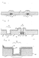
- an integrated circuit device is to be formed in a substrate 10 .
- Gate electrodes 12 are formed over the substrate 10 and spaced therefrom by gate oxide layer 14 .
- Sidewall spacers 16 are formed along side the gate electrodes 12 as known in the art.
- An interlevel insulating layer 18 is formed over the entire surface of the device.
- Interlevel insulating layer 18 can be, for example, a conformally deposited undoped oxide, a reflow glass or spin on glass, or a combination of different insulating layers. Formation of the structures described so far are conventional, and well known in the art.
- Openings 20 and 22 are formed through the interlevel insulating layer 18 . Opening 20 contacts the substrate 10 while opening 22 exposes a portion of the gate electrode 12 .
- those portions of the substrate 10 exposed in the opening 20 are silicided to form a silicided contact region 24 .
- a layer 26 of CVD nitride is then deposited over the surface of the device. This conformal layer 26 fills the sides and bottoms of the openings 20 , 22 , and provides a diffusion barrier for a metal interconnect layer (not shown) to be deposited later over the device.
- a number of process alternatives are provided for by the present invention. These are discussed in more detail in connection with Figure 4 , but generally include the introduction of oxygen into the nitride layer 26 . A small amount of oxygen diffuses into the nitride layer 26 , improving its resistance to the migration of silicon and aluminum atoms during later processing steps.
- the wafer containing the integrated circuit is placed into a sputtering machine.
- a titanium layer 28 is sputtered over the device in an argon atmosphere, preferably to a thickness of approximately 600 angstroms.
- Nitrogen is then introduced into the atmosphere of the sputtering chamber, while deposition of the titanium continues.
- This forms a titanium nitride layer 30 over the surface of the device, preferably to a thickness of approximately 1000 angstroms.
- the device is subjected to a thermal process, preferably a rapid thermal anneal, which forms a silicide region 32 below the opening 20 .
- the entire thickness of the nitride layer 30 is substantially stochiometric (1:1). This provides an improved diffusion barrier when compared with prior art techniques of converting a previously deposited titanium layer to titanium nitride. Deposition of the stochiometric nitride layer also occurs with the alternative arrangement shown in Figure 2 .
- the wafer containing the integrated circuit device is preferably exposed to an atmosphere containing oxygen after formation of either the nitride layer 26 or the nitride layer 30 .
- this can be performed in conjunction with a thermal treatment to enhance the diffusion of oxygen atoms into the nitride layer 26 , 30 .
- the nitride layer was substantially stochiometric, the resulting layer still contains approximately even proportions of titanium and nitrogen, with small amounts of oxygen.
- oxygen can actually be included in the titanium nitride layers 26 and 30 as they are formed.
- the nitrogen is introduced into the atmosphere of the sputtering chamber, small amounts of oxygen may also be introduced. This will cause small amounts of oxygen to be formed directly in the titanium nitride layer 30 , so that a later oxygen diffusion step is not required.
- it remains desirable to perform a thermal anneal of the device in order to form the silicide layer region 32 which improves contact resistance.
- FIG 4 two flow charts are shown which illustrate some of the process steps just described.
- Figure 4(a) illustrates the alternative shown in connection with Figure 3 .
- titanium is sputtered onto the device in argon 40 .
- nitrogen and oxygen are introduced into the atmosphere of the sputtering chamber 42 .
- Sputtering continues 44 , forming a nitride layer having small amounts of oxygen included therein. If desired, the oxygen may be left out when the nitrogen is introduced in step 42 , and diffused into the resulting nitride layer during the later anneal step.
- FIG. 4(b) illustrates several optional steps which can be used to introduce oxygen into the titanium nitride layer as described above.
- the titanium nitride layer is deposited 50 .
- small amounts of oxygen may be deposited with the titanium nitride layer, but this discussion will assume that this was not the case.
- the flow lines of the flow chart of Figure 4(b) may be followed in any combination.
- oxygen may be introduced into the nitride layer in a plasma environment 52 after the formation of the nitride layer 26 or 30 has been completed.
- the wafer containing the device may be moved to a separate chamber in a multichamber machine, and exposed to oxygen in such chamber 54 . Finally, the wafer may be moved to a rapid thermal processor, and subjected to an anneal in an ambient containing nitrogen with small amounts of oxygen.
- the three oxygen diffusion steps 52 , 54 , 56 may be selected and performed in any combination.
- any of them can be performed on a titanium nitride layer 26 , 30 which was formed with oxygen initially available in the ambient atmosphere during sputtering or CVD deposition.
- the oxygen plasma step 52 is typically performed after deposition is complete, and may be performed at a partial pressure of oxygen of approximately 10 ⁇ 5 torr to 10 ⁇ 2 torr , at a temperature of between 100°C and 500°C. If the wafer is moved to a separate chamber (step 54 ), the wafer may be exposed to an atmosphere of oxygen and argon at a temperature of between approximately room temperature and 500°C.
- a thermal anneal step in oxygen 56 is preferably performed in an atmosphere containing nitrogen and oxygen at a temperature in the range of approximately 450° to 750°C.
- formation of the titanium nitride layer according to the described embodiments results in an improved diffusion barrier layer. This is believed to be caused by a stuffing of the grain boundaries of the titanium nitride by oxygen and nitrogen atoms during and after the nitride layer formation. This inhibits the mobility of aluminum and silicon atoms through the nitride layer between grain boundaries.
- a thicker layer of substantially stochiometric titanium nitride is formed than in the case of prior art techniques, and an improved diffusion barrier layer results.
- This improved diffusion barrier minimizes intermingling of aluminum and silicon atoms at contact regions, preventing detrimental side affects of such intermingling as is known in the art.
Abstract
A method for forming interlevel contacts in integrated circuits includes the formation of a titanium nitride layer (26) prior to formation of an overlying conductive layer of a material such as polycrystalline silicon or a metal. In one approach, CVD titanium nitride (26) is deposited over a partially formed integrated circuit device and in a contact opening (20). The titanium nitride layer (26) is then exposed to an atmosphere containing oxygen, so that oxygen atoms diffuse into the titanium nitride layer (26). This may be done in conjunction with an annealing step. In another embodiment, layers of titanium (28) and titanium nitride (30) are sequentially sputtered onto the device. The nitride layer may then be exposed to an oxygen ambient, or the oxygen may be incorporated into the titanium nitride layer during the sputter deposition.
Description
- The present invention relates generally to the formation of integrated circuit devices, and more specifically to the formation of low resistance interlevel contact sensitive devices.
- In integrated circuit devices, contact resistance is between interconnect levels is important. This is especially true in small devices, in which the small areas available for interlevel contacts can result in resistances high enough to adversely impact device performance. It is also important to provide a diffusion barrier between aluminum and silicon to prevent silicon spiking, especially with the shallow junctions prevalent with high density devices. Many different techniques have been proposed and implemented to reduce contact resistances, while simultaneously minimizing interdiffusion of underlying silicon atoms and aluminum atoms from a metal interconnect structure.
- One approach is to deposit a barrier metal in the contact prior to deposition of an aluminum interconnect layer. When a barrier metal such as titanium is used, it can be silicided in order to reduce the contact resistance. The titanium can also be used to form a barrier layer. One approach which has been used in the past is to deposit titanium over the integrated circuit device after contact openings have been formed, and then anneal the titanium in a nitrogen ambient atmosphere. This causes silicidation of the titanium in the contact opening, and forms a diffusion barrier layer of titanium nitride in the upper portions of the titanium layer. Thus, portions of the titanium layer are converted to titanium nitride while other portions are simultaneously converted to titanium silicide.
- While this approach provides enhanced barrier performance, the quality of the titanium nitride barrier in preventing migration of aluminum in silicon atoms is not as good as might be desired. With the conversion process described above, only a very thin top layer of the titanium is converted to stochiometric (1:1) titanium nitride. Below this thin top layer, typically approximately 20 angstroms thick, the ratio of nitrogen to titanium is relatively low. Thus the majority of the nitride layer is actually TiNx, where x typically has a value in the range

- It would therefore be desirable to provide a technique for forming a titanium nitride barrier layer which has improved properties over prior art techniques. It is extremely desirable for such a technique to be compatible with current device processing techniques.
- Therefore, according to the present invention, a method for forming interlevel contacts in integrated circuits includes the formation of a titanium nitride layer prior to formation of an overlying conductive layer of a material such as polycrystalline silicon or a metal. In one approach, CVD titanium nitride is deposited over a partially formed integrated circuit device and in a contact opening. The titanium nitride layer is then exposed to an atmosphere containing oxygen, so that oxygen atoms diffuse into the titanium nitride layer. This may be done in conjunction with an annealing step. In another embodiment, layers of titanium and titanium nitride are sequentially sputtered onto the device. The nitride layer may then be exposed to various oxygen treatments, or the oxygen may be incorporated into the titanium nitride layer during the sputter deposition.
- The novel features believed characteristic of the invention are set forth in the appended claims. The invention itself however, as well as a preferred mode of use, and further objects and advantages thereof, will best be understood by reference to the following detailed description of an illustrative embodiment when read in conjunction with the accompanying drawings, wherein:
- Figures 1 - 3 illustrate sections of an integrated circuit device during formation of contacts in accordance with the present invention; and
- Figure 4 describes techniques for forming portions of the inventive method in flowchart form.
- The process steps and structures described below do not form a complete process flow for manufacturing integrated circuits. The present invention can be practiced in conjunction with integrated circuit fabrication techniques currently used in the art, and only so much of the commonly practiced process steps are included as are necessary for an understanding of the present invention. The figures representing cross-sections of portions of an integrated circuit during fabrication are not drawn to scale, but instead are drawn so as to illustrate the important features of the invention.
- Referring to Figure 1, an integrated circuit device is to be formed in a
substrate 10.Gate electrodes 12 are formed over thesubstrate 10 and spaced therefrom bygate oxide layer 14.Sidewall spacers 16 are formed along side thegate electrodes 12 as known in the art. An interlevel insulatinglayer 18 is formed over the entire surface of the device.Interlevel insulating layer 18 can be, for example, a conformally deposited undoped oxide, a reflow glass or spin on glass, or a combination of different insulating layers. Formation of the structures described so far are conventional, and well known in the art. - Referring to Figure 2 an enlarged view of the section shown in Figure 1 is illustrated.
Openings 20 and 22 are formed through the interlevel insulatinglayer 18. Opening 20 contacts thesubstrate 10 while opening 22 exposes a portion of thegate electrode 12. - In one preferred embodiment, those portions of the
substrate 10 exposed in theopening 20 are silicided to form asilicided contact region 24. Alayer 26 of CVD nitride is then deposited over the surface of the device. Thisconformal layer 26 fills the sides and bottoms of theopenings 20, 22, and provides a diffusion barrier for a metal interconnect layer (not shown) to be deposited later over the device. Once theCVD nitride 26 has been deposited, a number of process alternatives are provided for by the present invention. These are discussed in more detail in connection with Figure 4, but generally include the introduction of oxygen into thenitride layer 26. A small amount of oxygen diffuses into thenitride layer 26, improving its resistance to the migration of silicon and aluminum atoms during later processing steps. - Referring to Figure 3 an alternative nitride formation technique is shown. Once the
contact opening 20 has been formed, the wafer containing the integrated circuit is placed into a sputtering machine. A titanium layer 28 is sputtered over the device in an argon atmosphere, preferably to a thickness of approximately 600 angstroms. Nitrogen is then introduced into the atmosphere of the sputtering chamber, while deposition of the titanium continues. This forms atitanium nitride layer 30 over the surface of the device, preferably to a thickness of approximately 1000 angstroms. After formation of thenitride layer 30, the device is subjected to a thermal process, preferably a rapid thermal anneal, which forms a silicide region 32 below theopening 20. - Since nitrogen was present to react with the titanium during its deposition, the entire thickness of the
nitride layer 30 is substantially stochiometric (1:1). This provides an improved diffusion barrier when compared with prior art techniques of converting a previously deposited titanium layer to titanium nitride. Deposition of the stochiometric nitride layer also occurs with the alternative arrangement shown in Figure 2. - In both of the embodiments described in Figures 2 and 3, the wafer containing the integrated circuit device is preferably exposed to an atmosphere containing oxygen after formation of either the
nitride layer 26 or thenitride layer 30. As described above, this can be performed in conjunction with a thermal treatment to enhance the diffusion of oxygen atoms into thenitride layer - With either of the embodiments described in connection with Figures 2 and 3, oxygen can actually be included in the
titanium nitride layers titanium nitride layer 30, so that a later oxygen diffusion step is not required. With the method of Figure 3, it remains desirable to perform a thermal anneal of the device in order to form the silicide layer region 32 which improves contact resistance. - Referring to Figure 4, two flow charts are shown which illustrate some of the process steps just described. Figure 4(a) illustrates the alternative shown in connection with Figure 3. Once the opening has been formed, titanium is sputtered onto the device in argon 40. While the sputtering continues, nitrogen and oxygen are introduced into the atmosphere of the sputtering chamber 42. Sputtering continues 44, forming a nitride layer having small amounts of oxygen included therein. If desired, the oxygen may be left out when the nitrogen is introduced in step 42, and diffused into the resulting nitride layer during the later anneal step.
- Figure 4(b) illustrates several optional steps which can be used to introduce oxygen into the titanium nitride layer as described above. Initially, the titanium nitride layer is deposited 50. In any of the preferred embodiments, small amounts of oxygen may be deposited with the titanium nitride layer, but this discussion will assume that this was not the case. The flow lines of the flow chart of Figure 4(b) may be followed in any combination. Thus, oxygen may be introduced into the nitride layer in a plasma environment 52 after the formation of the
nitride layer - As illustrated in the flowchart, the three oxygen diffusion steps 52, 54, 56 may be selected and performed in any combination. In addition, any of them can be performed on a
titanium nitride layer - The oxygen plasma step 52 is typically performed after deposition is complete, and may be performed at a partial pressure of oxygen of approximately 10⁻⁵ torr to 10⁻² torr , at a temperature of between 100°C and 500°C. If the wafer is moved to a separate chamber (step 54), the wafer may be exposed to an atmosphere of oxygen and argon at a temperature of between approximately room temperature and 500°C. A thermal anneal step in
oxygen 56 is preferably performed in an atmosphere containing nitrogen and oxygen at a temperature in the range of approximately 450° to 750°C. - As will be appreciated by those skilled in the art, formation of the titanium nitride layer according to the described embodiments results in an improved diffusion barrier layer. This is believed to be caused by a stuffing of the grain boundaries of the titanium nitride by oxygen and nitrogen atoms during and after the nitride layer formation. This inhibits the mobility of aluminum and silicon atoms through the nitride layer between grain boundaries.
- As will be appreciated by those skilled in the art, the various described techniques are easily performed using standard process flows and do not require any special equipment. A thicker layer of substantially stochiometric titanium nitride is formed than in the case of prior art techniques, and an improved diffusion barrier layer results. This improved diffusion barrier minimizes intermingling of aluminum and silicon atoms at contact regions, preventing detrimental side affects of such intermingling as is known in the art.
- While the invention has been particularly shown and described with reference to a preferred embodiment, it will be understood by those skilled in the art that various changes in form and detail may be made therein without departing from the spirit and scope of the invention.
Claims (17)
- A method for forming a barrier layer on an integrated circuit device, comprising the steps of:
forming an insulating layer over the device;
forming an opening through the insulating layer to expose a portion of an underlying conducting layer;
forming a layer of titanium nitride over the insulating layer and in the opening; and
exposing the titanium nitride layer to an ambient atmosphere containing oxygen to cause oxygen molecules to diffuse into the titanium nitride layer. - The method of Claim 1, wherein the underlying conductive layer comprises a semiconductor substrate.
- The method of Claim 1, wherein said step of forming a layer of titanium nitride comprises the step of:
depositing a layer of substantially stoichiometric titanium nitride over the device. - The method of Claim 3, wherein the titanium nitride layer is formed by chemical vapor deposition.
- The method of Claim 3, wherein said depositing step comprises the steps of:
depositing a layer of titanium in a nonreactive ambient atmosphere;
introducing nitrogen into the ambient atmosphere; and
depositing titanium reacted with the nitrogen to form titanium nitride. - The method of Claim 5, wherein the titanium layer is deposited in an atmosphere containing argon.
- The method of Claim 5, wherein said introducing step further includes introducing oxygen into the ambient atmosphere.
- The method of Claim 5, further comprising the step of:
thermally annealing the device after depositing the titanium nitride, wherein titanium silicide is formed in the exposed portion of the underlying conducting layer. - The method of Claim 1, wherein said exposing step comprises the step of:
exposing the titanium nitride layer to an oxygen plasma. - The method of Claim 1, wherein said exposing step comprises the step of:
exposing the titanium nitride layer to an atmosphere containing oxygen and argon at a temperature of between 100 and 500 degrees C. - The method of Claim 1, wherein said step of forming the titanium nitride layer comprises the step of:
providing an ambient atmosphere containing oxygen; and
depositing the titanium nitride over the device, wherein oxygen atoms are included in the titanium nitride layer. - A barrier layer structure for an integrated circuit device, comprising:
an insulating layer overlying a conductive structure;
an opening through said insulating layer which exposes a portion of the underlying conductive structure;
a barrier metal layer overlying a portion of the insulating layer and said opening, said barrier metal layer containing oxygen atoms therein. - The structure of Claim 12, wherein said barrier metal layer comprises titanium nitride.
- The structure of Claim 13, wherein said barrier metal layer comprises substantially stoichiometric titanium nitride throughout its thickness.
- The structure of Claim 12, wherein said barrier metal layer comprises:
a layer of titanium in contact with said insulating layer and the underlying conductive layer; and
a layer of substantially stoichiometric titanium nitride overlying said titanium layer, said titanium nitride containing oxygen atoms diffused thereinto. - The structure of Claim 15, wherein said titanium nitride layer comprises a layer of material formed by sputtering titanium nitride over said titanium layer in an atmosphere containing oxygen.
- The structure of Claim 15, wherein said titanium nitride layer comprises a layer of material formed by sputtering titanium nitride over said titanium layer in an atmosphere not containing oxygen, followed by diffusing oxygen into said titanium nitride layer from an upper surface thereof.
Applications Claiming Priority (2)
| Application Number | Priority Date | Filing Date | Title |
|---|---|---|---|
| US80085591A | 1991-11-26 | 1991-11-26 | |
| US800855 | 1991-11-26 |
Publications (1)
| Publication Number | Publication Date |
|---|---|
| EP0545602A1 true EP0545602A1 (en) | 1993-06-09 |
Family
ID=25179552
Family Applications (1)
| Application Number | Title | Priority Date | Filing Date |
|---|---|---|---|
| EP92310724A Withdrawn EP0545602A1 (en) | 1991-11-26 | 1992-11-24 | Method for forming barrier metal layers |
Country Status (2)
| Country | Link |
|---|---|
| EP (1) | EP0545602A1 (en) |
| JP (1) | JPH05267211A (en) |
Cited By (16)
| Publication number | Priority date | Publication date | Assignee | Title |
|---|---|---|---|---|
| EP0551117A2 (en) * | 1992-01-08 | 1993-07-14 | Mitsubishi Denki Kabushiki Kaisha | Large scale integrated circuit device and thin film forming method and apparatus for the same |
| EP0680077A1 (en) * | 1994-04-29 | 1995-11-02 | STMicroelectronics, Inc. | Integrated circuit with improved contact barrier |
| GB2290166A (en) * | 1994-06-10 | 1995-12-13 | Samsung Electronics Co Ltd | Wiring structure and method of manufacture |
| GB2291264A (en) * | 1994-07-07 | 1996-01-17 | Hyundai Electronics Ind | Method for forming a metallic barrier layer |
| EP0732731A2 (en) * | 1995-03-13 | 1996-09-18 | Applied Materials, Inc. | Treatment of a titanium nitride layer to improve resistance to elevated temperatures |
| EP0747500A1 (en) * | 1995-06-07 | 1996-12-11 | Applied Materials, Inc. | Process for forming improved titanium containing barrier layers |
| EP0867941A2 (en) * | 1997-03-28 | 1998-09-30 | Applied Materials, Inc. | An interconnect structure for use in an intergrated circuit |
| US5858184A (en) * | 1995-06-07 | 1999-01-12 | Applied Materials, Inc. | Process for forming improved titanium-containing barrier layers |
| US5895266A (en) * | 1996-02-26 | 1999-04-20 | Applied Materials, Inc. | Titanium nitride barrier layers |
| US6069073A (en) * | 1997-09-18 | 2000-05-30 | Electronics And Telecommunications Research Institute | Method for forming diffusion barrier layers |
| US6155198A (en) * | 1994-11-14 | 2000-12-05 | Applied Materials, Inc. | Apparatus for constructing an oxidized film on a semiconductor wafer |
| US6291343B1 (en) | 1994-11-14 | 2001-09-18 | Applied Materials, Inc. | Plasma annealing of substrates to improve adhesion |
| US6365495B2 (en) | 1994-11-14 | 2002-04-02 | Applied Materials, Inc. | Method for performing metallo-organic chemical vapor deposition of titanium nitride at reduced temperature |
| US6475907B1 (en) * | 1999-04-20 | 2002-11-05 | Nec Corporation | Semiconductor device having a barrier metal layer and method for manufacturing the same |
| US6699530B2 (en) | 1995-07-06 | 2004-03-02 | Applied Materials, Inc. | Method for constructing a film on a semiconductor wafer |
| DE19751785B4 (en) * | 1996-11-22 | 2004-08-05 | Trikon Equipments Ltd., Newport | Process for treating a semiconductor wafer |
Families Citing this family (1)
| Publication number | Priority date | Publication date | Assignee | Title |
|---|---|---|---|---|
| KR100187669B1 (en) * | 1996-01-30 | 1999-06-01 | 김주용 | Method for forming diffusion preventing film of semiconductor device |
Citations (4)
| Publication number | Priority date | Publication date | Assignee | Title |
|---|---|---|---|---|
| JPS63164315A (en) * | 1986-12-26 | 1988-07-07 | Oki Electric Ind Co Ltd | Manufacture of semiconductor device |
| JPH0254926A (en) * | 1988-08-19 | 1990-02-23 | Seiko Epson Corp | Manufacture of semiconductor device |
| JPH02291124A (en) * | 1989-04-28 | 1990-11-30 | Fujitsu Ltd | Manufacture of semiconductor device |
| JPH03153077A (en) * | 1989-11-10 | 1991-07-01 | Seiko Epson Corp | Semiconductor device |
-
1992
- 1992-11-24 EP EP92310724A patent/EP0545602A1/en not_active Withdrawn
- 1992-11-25 JP JP31536292A patent/JPH05267211A/en active Pending
Patent Citations (4)
| Publication number | Priority date | Publication date | Assignee | Title |
|---|---|---|---|---|
| JPS63164315A (en) * | 1986-12-26 | 1988-07-07 | Oki Electric Ind Co Ltd | Manufacture of semiconductor device |
| JPH0254926A (en) * | 1988-08-19 | 1990-02-23 | Seiko Epson Corp | Manufacture of semiconductor device |
| JPH02291124A (en) * | 1989-04-28 | 1990-11-30 | Fujitsu Ltd | Manufacture of semiconductor device |
| JPH03153077A (en) * | 1989-11-10 | 1991-07-01 | Seiko Epson Corp | Semiconductor device |
Non-Patent Citations (4)
| Title |
|---|
| PATENT ABSTRACTS OF JAPAN vol. 012, no. 425 (E-681)10 November 1988 & JP-A-63 164 315 * |
| PATENT ABSTRACTS OF JAPAN vol. 014, no. 222 (E-0926)10 May 1990 & JP-A-02 054 926 ( SEIKO EPSON CORP. ) 23 February 1990 * |
| PATENT ABSTRACTS OF JAPAN vol. 015, no. 070 (E-1035)19 February 1991 & JP-A-02 291 124 ( FUJITSU LTD ) 30 November 1990 * |
| PATENT ABSTRACTS OF JAPAN vol. 015, no. 383 (E-1116)27 September 1991 & JP-A-03 153 077 ( SEIKO EPSON CORP ) 1 July 1991 * |
Cited By (30)
| Publication number | Priority date | Publication date | Assignee | Title |
|---|---|---|---|---|
| EP0551117A3 (en) * | 1992-01-08 | 1995-06-07 | Mitsubishi Electric Corp | |
| EP0551117A2 (en) * | 1992-01-08 | 1993-07-14 | Mitsubishi Denki Kabushiki Kaisha | Large scale integrated circuit device and thin film forming method and apparatus for the same |
| EP0680077A1 (en) * | 1994-04-29 | 1995-11-02 | STMicroelectronics, Inc. | Integrated circuit with improved contact barrier |
| US5514908A (en) * | 1994-04-29 | 1996-05-07 | Sgs-Thomson Microelectronics, Inc. | Integrated circuit with a titanium nitride contact barrier having oxygen stuffed grain boundaries |
| US6191033B1 (en) | 1994-04-29 | 2001-02-20 | Stmicroelectronics, Inc. | Method of fabricating an integrated circuit with improved contact barrier |
| US5652464A (en) * | 1994-04-29 | 1997-07-29 | Sgs-Thomson Microelectronics, Inc. | Integrated circuit with a titanium nitride contact barrier having oxygen stuffed grain boundaries |
| US6291344B1 (en) * | 1994-04-29 | 2001-09-18 | Stmicroelectronics, Inc. | Integrated circuit with improved contact barrier |
| GB2290166B (en) * | 1994-06-10 | 1998-09-09 | Samsung Electronics Co Ltd | Manufacturing method for a wiring structure of a semiconductor device |
| GB2290166A (en) * | 1994-06-10 | 1995-12-13 | Samsung Electronics Co Ltd | Wiring structure and method of manufacture |
| US5998870A (en) * | 1994-06-10 | 1999-12-07 | Samsung Electronics Co., Ltd. | Wiring structure of semiconductor device and method for manufacturing the same |
| GB2291264A (en) * | 1994-07-07 | 1996-01-17 | Hyundai Electronics Ind | Method for forming a metallic barrier layer |
| GB2291264B (en) * | 1994-07-07 | 1998-07-29 | Hyundai Electronics Ind | Method for forming a metallic barrier layer in semiconductor device and device made by the method |
| US6365495B2 (en) | 1994-11-14 | 2002-04-02 | Applied Materials, Inc. | Method for performing metallo-organic chemical vapor deposition of titanium nitride at reduced temperature |
| US6291343B1 (en) | 1994-11-14 | 2001-09-18 | Applied Materials, Inc. | Plasma annealing of substrates to improve adhesion |
| US6155198A (en) * | 1994-11-14 | 2000-12-05 | Applied Materials, Inc. | Apparatus for constructing an oxidized film on a semiconductor wafer |
| EP0732731A3 (en) * | 1995-03-13 | 1997-10-08 | Applied Materials Inc | Treatment of a titanium nitride layer to improve resistance to elevated temperatures |
| US5943600A (en) * | 1995-03-13 | 1999-08-24 | Applied Materials, Inc. | Treatment of a titanium nitride layer to improve resistance to elevated temperatures |
| EP0732731A2 (en) * | 1995-03-13 | 1996-09-18 | Applied Materials, Inc. | Treatment of a titanium nitride layer to improve resistance to elevated temperatures |
| EP0747500A1 (en) * | 1995-06-07 | 1996-12-11 | Applied Materials, Inc. | Process for forming improved titanium containing barrier layers |
| US6007684A (en) * | 1995-06-07 | 1999-12-28 | Applied Materials, Inc. | Process for forming improved titanium-containing barrier layers |
| US5972178A (en) * | 1995-06-07 | 1999-10-26 | Applied Materials, Inc. | Continuous process for forming improved titanium nitride barrier layers |
| US5858184A (en) * | 1995-06-07 | 1999-01-12 | Applied Materials, Inc. | Process for forming improved titanium-containing barrier layers |
| US6699530B2 (en) | 1995-07-06 | 2004-03-02 | Applied Materials, Inc. | Method for constructing a film on a semiconductor wafer |
| US6238803B1 (en) | 1996-02-26 | 2001-05-29 | Applied Materials, Inc. | Titanium nitride barrier layers |
| US5895266A (en) * | 1996-02-26 | 1999-04-20 | Applied Materials, Inc. | Titanium nitride barrier layers |
| DE19751785B4 (en) * | 1996-11-22 | 2004-08-05 | Trikon Equipments Ltd., Newport | Process for treating a semiconductor wafer |
| EP0867941A3 (en) * | 1997-03-28 | 2000-04-05 | Applied Materials, Inc. | An interconnect structure for use in an intergrated circuit |
| EP0867941A2 (en) * | 1997-03-28 | 1998-09-30 | Applied Materials, Inc. | An interconnect structure for use in an intergrated circuit |
| US6069073A (en) * | 1997-09-18 | 2000-05-30 | Electronics And Telecommunications Research Institute | Method for forming diffusion barrier layers |
| US6475907B1 (en) * | 1999-04-20 | 2002-11-05 | Nec Corporation | Semiconductor device having a barrier metal layer and method for manufacturing the same |
Also Published As
| Publication number | Publication date |
|---|---|
| JPH05267211A (en) | 1993-10-15 |
Similar Documents
| Publication | Publication Date | Title |
|---|---|---|
| US7443032B2 (en) | Memory device with chemical vapor deposition of titanium for titanium silicide contacts | |
| EP0545602A1 (en) | Method for forming barrier metal layers | |
| JP3132750B2 (en) | Multilayer structure, semiconductor structure, capacitor of semiconductor device, method of preventing oxidation of silicon structure, and method of preventing diffusion of dopant | |
| US4920073A (en) | Selective silicidation process using a titanium nitride protective layer | |
| US6770571B2 (en) | Barrier in gate stack for improved gate dielectric integrity | |
| US6410427B1 (en) | Metal silicidation methods and methods for using same | |
| US6524953B1 (en) | Asymmetric, double-sided self-aligned silicide and method of forming the same | |
| US5907784A (en) | Method of making multi-layer gate structure with different stoichiometry silicide layers | |
| US5677244A (en) | Method of alloying an interconnect structure with copper | |
| JPH08191054A (en) | Semiconductor device and manufacture thereof | |
| CA2043172C (en) | Method and structure for interconnecting different polysilicon zones on semi-conductor substrates for integrated circuits | |
| JP3213909B2 (en) | Resistor and method of manufacturing the same | |
| JPH08264448A (en) | Preparation of formation of titanium silicide of minute titanium nitridation film and minute titanium nitridation film thin film and semiconductor element using it | |
| US5421974A (en) | Integrated circuit having silicide-nitride based multi-layer metallization | |
| US20060202283A1 (en) | Metal silicide adhesion layer for contact structures | |
| US6433434B1 (en) | Apparatus having a titanium alloy layer | |
| US6403458B2 (en) | Method for fabricating local interconnect structure for integrated circuit devices, source structures | |
| KR100209931B1 (en) | Silicide making method for semiconductor device | |
| US20020175413A1 (en) | Method for utilizing tungsten barrier in contacts to silicide and structure produced therby | |
| US20010019159A1 (en) | Local interconnect structure for integrated circuit devices, source structure for the same, and method for fabricating the same | |
| JPH0748495B2 (en) | Method for manufacturing semiconductor device | |
| Yoo et al. | Peeling-free tungsten polycide process and its application in DRAM fabrication | |
| JPH0513366A (en) | Method of wiring for contact | |
| JPH04318925A (en) | Transistor and manufacture thereof | |
| KR20030050846A (en) | Method for forming metal line of semiconductor |
Legal Events
| Date | Code | Title | Description |
|---|---|---|---|
| PUAI | Public reference made under article 153(3) epc to a published international application that has entered the european phase |
Free format text: ORIGINAL CODE: 0009012 |
|
| AK | Designated contracting states |
Kind code of ref document: A1 Designated state(s): DE FR GB IT |
|
| STAA | Information on the status of an ep patent application or granted ep patent |
Free format text: STATUS: THE APPLICATION IS DEEMED TO BE WITHDRAWN |
|
| 18D | Application deemed to be withdrawn |
Effective date: 19940221 |