EP0547836B1 - Optical packet switch - Google Patents
Optical packet switch Download PDFInfo
- Publication number
- EP0547836B1 EP0547836B1 EP92311260A EP92311260A EP0547836B1 EP 0547836 B1 EP0547836 B1 EP 0547836B1 EP 92311260 A EP92311260 A EP 92311260A EP 92311260 A EP92311260 A EP 92311260A EP 0547836 B1 EP0547836 B1 EP 0547836B1
- Authority
- EP
- European Patent Office
- Prior art keywords
- optical
- data packets
- inputs
- packet
- optical data
- Prior art date
- Legal status (The legal status is an assumption and is not a legal conclusion. Google has not performed a legal analysis and makes no representation as to the accuracy of the status listed.)
- Expired - Lifetime
Links
Images


Classifications
-
- H—ELECTRICITY
- H04—ELECTRIC COMMUNICATION TECHNIQUE
- H04Q—SELECTING
- H04Q11/00—Selecting arrangements for multiplex systems
- H04Q11/0001—Selecting arrangements for multiplex systems using optical switching
-
- H—ELECTRICITY
- H04—ELECTRIC COMMUNICATION TECHNIQUE
- H04Q—SELECTING
- H04Q11/00—Selecting arrangements for multiplex systems
- H04Q11/0001—Selecting arrangements for multiplex systems using optical switching
- H04Q11/0062—Network aspects
- H04Q11/0066—Provisions for optical burst or packet networks
Landscapes
- Engineering & Computer Science (AREA)
- Computer Networks & Wireless Communication (AREA)
- Optical Communication System (AREA)
- Data Exchanges In Wide-Area Networks (AREA)
Description
- This invention relates to optical packet switches and, more particularly, to optical packet switches which switch data packets in the optical domain.
- Packet switches are designed to avoid collisions of the packets of data that are being switched. Collisions of data packets occur within a switch when two data packets arrive at the inputs to the switch at the same time and are destined for the same switch output. While the switching mechanism can switch one packet to the appropriate output, the other data packet cannot be accommodated by the switching mechanism. The second data packet consequently is blocked from reaching its destination. As a result, the second data packet is destroyed and data are lost.
- Optical packet switches are switches which switch data packets in the optical domain. Data packets remain as optical signals throughout the entire switching process. Optical packet switches, like other packet switches, are designed to avoid data packet collisions.
- Chlamtac et al., "QUADRO-Stars: High Performance Optical WDM Star Networks", IEEE Global Telecommunications Conference, 2-5 December 1991, pages 1224-1229, describes a wavelength division multiplexing (WDM) system in which signals generated by tunable lasers at transmitting stations are input to a switching hub. The switching hub receives signals at multiple inputs and switches the signals to multiple outputs using conventional WDM techniques. Attached to each output of the hub is a receiver that receives signals at a predetermined wavelength. Each receiver includes optical delay lines, which are used as buffers.
- Tamir et al., "High Performance Multi-Queue Buffers for VLSI Communication Switches", 15th Annual International Symposium on Computer Architecture, 30 May-June 1988, pages 343-354, discloses small n x n switches for multistage interconnection networks used in multiprocessors as well as in the communication coprocessors used in multi-computers. This switch uses a dynamically allocated multi-queue buffer to provide handling and forwarding of variable length packets in non-FIFO order.
- Obara, "Distributed ATM Cross-Connect Switch Architecture Using Schedule Control", Electronics and Communications in Japan, Part I-Communications, Vol. 74, No. 1, January 1991, pages 55-64, discloses a scheduling control method which dynamically assigns cell transmission time. The scheduling method aligns the cell for input to the switch. After the switching stage, the cell is then stored in a buffer.
- Tsukada et al., "Ultra Fast Photonic ATM Switch Based on Time-Division Broadcast-and-Select Network", IEEE Global Telecommunications Conference, 2-5 December 1991, pages 1230-1234, discloses a hardware implementation and design for an ultrafast photonic ATM (ULPHA) switch. The ULPHA switch has high throughput from using ultrafast optical pulses for cell signals in order to avoid cell contentions through optical output buffers. The optical output buffers, in the form of delay lines, are located on the output side of the switch.
- One common technique for avoiding packet collisions in an optical packet switch is to switch contending data packets into optical recirculation storage devices such as recirculating loops. An optical recirculating loop stores an optical data packet by confining the data packet in a loop of optical fiber until such time as it is desirable to extract the data packet from the loop. The stored data packets can be retrieved at a convenient time, such as when a contention no longer exists within the switch. In this way, a packet that otherwise would be destroyed is stored in the recirculating loop.
- Recirculation storage devices, however, are prohibitively expensive to use. For example, recirculating loops require complex switching and control circuitry to function properly. Moreover, each recirculating loop must be provided with means for optically amplifying the recirculating data packet to compensate for losses resulting from recirculation and switching. Optical amplification adds expense and complexity to the system. It therefore would be desirable to provide an optical switch which switches data in the optical domain, but which does not rely on recirculation storage devices.
- Optical recirculation storage devices are eliminated from an optical switch while simultaneously achieving improved non- blocking performance of the switch by providing a feed-forward packet delay arrangement in which data packets are staggered in time so as to avoid collisions of data packets at the switch output.
- The optical switch preferably includes two non-blocking stages which are coupled by optical delay lines of progressively larger feed-forward delays. The non-blocking stages include a scheduling stage and a switching stage. Data packets are irretrievably inserted into the delay lines by the scheduling stage. The delay lines stagger in time the arrival of the data packets at the switching stage. Data packets are staggered to resolve contentions between packets and thereby avoid packet collisions in the switching stage of the optical switch. Packets are switched to the appropriate destination by the switching stage. Data packets remain in the optical domain throughout the switching operation.
- The above and other advantages of the invention will be apparent upon consideration of the following detailed description taken in conjunction with the accompanying drawings in which like reference numbers refer to like parts throughout and in which:
- FIG. 1 is a block diagram of a portion of an optical transmission system which includes the optical packet switch of the present invention;
- FIG. 2 is a functional block diagram of the optical packet switch of FIG. 1;
- FIG. 3 is a block diagram of the architecture of the switch of FIG. 1;
- FIG. 4 is a graph of the probability of blockage for different availability of delay lines;
- FIG. 5 is a block diagram of a Benes network suitable for use in the scheduling and switching stages of FIG. 3;
- FIG. 6 is a schematic diagram of the detector circuit of FIG. 3;
- FIG. 7 is a schematic diagram of the control circuitry of FIG. 3; and
- FIG. 8 is a block diagram of an illustrative embodiment of a synchronization circuit for use in the optical packet switch of FIG. 3.
-
- Optical packet switching is accomplished in the optical domain accordance with the principles of the present invention by providing an all-optical switch which staggers in time contending data packets so as to avoid collisions. An exemplary embodiment of such a switch includes a scheduling stage which couples optical data packets to feed-forward optical delay lines of progressively larger delay so as to avoid packet collisions and a switching stage for completing the switching operation. Data packets enter the scheduling stage and are output via optical delay lines to the switching stage. The scheduling stage irretrievably switches (i.e., "schedules") the data packets that arrive at the switch into the delay lines in such a way that no two data packets arriving at the switching stage in a given time slot are destined for the same switch output. Collisions are avoided by resolving contentions between data packets (i.e., two packets destined for the same switch output at the same time) before the data packets arrive at the switching stage. Contentions are resolved by delaying (i.e., staggering in time) prospective colliding packets by at least one time slot. In this manner, data packets remain in the optical domain throughout the switching operation without the use of recirculation devices.
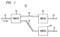
- FIG. 1 shows an illustrative application of the optical packet switch of the present invention. A portion of a
transmission system 10 is shown having several segments ofoptical fiber cable 12 coupled to each other via theoptical packet switches 14 constructed in accordance with the principles of the present invention. Eachcable 12 includes several optical fibers (not shown). Optical data packets are transmitted through cables 12 (in the direction indicated by the arrow). Data packets enteroptical packet switches 14 and are switched to the appropriate destination fiber in the appropriate cable at the output of eachswitch 14. - The operation of optical packet switch 4 will now be described with reference to FIG. 2.
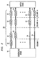
Optical packet switch 14 includes ascheduling stage 16 and a switchingstage 18.Stages Scheduling stage 16 outputs data packets received from an optical fiber (such ascable 12 of FIG. 1) to appropriate ones ofoptical delay lines 20. Eachbox 22 represents a one-packet delay, that is, a time delay sufficient to transfer one packet of data betweenscheduling stage 16 and switchingstage 18. As used herein, a one-packet delay equals one "time slot." The columns indicated on FIG. 2 represent a single time slot. For purposes of explanation herein, data packets that will reach switchingstage 18 in the same time slot are described as being within the same column. - Each
delay line 20 typically introduces a specific amount of delay in the transfer of data from schedulingstage 16 to switchingstage 18. Generally, the delay lines introduce different amounts of delay, however several lines may introduce the same amount of delay. For example, afirst delay line 24 introduces a one-packet delay (illustrated by a single box 22) betweenscheduling stage 16 and switchingstage 18. Asecond delay line 26 introduces a two-packet delay, as illustrated by twoboxes 22. Similarly, a straight-through path (not shown) could be provided betweenscheduling stage 16 and switchingstage 18. The variation in delay betweenlines scheduling stage 16 to stagger in time two data packets destined for the same switch output that reachswitch 14 at the same time. Thus,scheduling stage 16 can cause the data packets to reach switchingstage 18 at different times.Scheduling stage 16 ensures that no two packets in a time slot are destined for the same output.Scheduling stage 16 can thereby prevent collisions of those packets at switchingstage 18, and thus prevent data loss. -
Delay lines 20 are feed-forward and preferably deterministic in nature. Althoughdelay lines 20 are described as delay devices, one skilled in the art will appreciate that not all of the delay lines must be pure delay.Scheduling stage 16 irretrievably inserts data packets into one ofdelay lines 20. A data packet output by schedulingstage 16 to one ofdelay lines 20 will arrive at switchingstage 18 after a predetermined interval of time. In this manner, the optical switch of the present invention avoids the expense and complexity of recirculating loop technology. - Collisions of optical data packets are avoided at switching
stage 18 by staggering data packets in time such that within a given time slot each data packet presented to switchingstage 18 is routed to a different output of the switching stage. This is a direct consequence of the operation ofscheduling stage 16.Scheduling stage 16 receives data packets arriving atswitch 14 and inserts the data packets into delay lines of different delay such that when the data packets exit the delay lines at switchingstage 18, no more than one packet is destined for any given output in the same time slot. For example, two packets that arrive atswitch 14 in the same time slot and destined for the same switch output will be inserted into delay lines of different delay. The delay lines are of such delay that one of the packets will traverse the delay line in which it was inserted andclear switching stage 18 before the other packet has traversed its delay line. - One exemplary method for routing data packets arriving at
switch 14 in a given time slot to different switch outputs utilizes a sequential scanning technique, as described below. The term "scanning" refers to the process by which the incoming data packets are assigned priority for switching purposes. The inputs toscheduling stage 16 are sequentially scanned beginning with the lowest numbered input. For each input packet,scheduling stage 16 attempts to insert the packet in thedelay line 20 having the least amount of delay. In doing so, schedulingstage 16 ensures that no previous packet was inserted in the delay line in this time slot.Scheduling stage 16 also ensures that no other packet to the same destination (i.e., to the same output of switching stage 18) exists in the column (e.g., column m) in which the packet is to be inserted. The technique described above gives a higher priority to lower numbered inputs. Thus, the lower numbered inputs will have the smallest probability of blockage. Blockage is defined as the inability to accommodate a packet in any of the delay lines. - Other scanning techniques could be implemented for scheduling data packets on
delay lines 20 so as to assign different priorities to the inputs ofoptical switch 14. Implementation of these techniques would be apparent to one of ordinary skill in the art in view of this disclosure. Examples of two alternative scanning techniques are a random scanning technique and an output-based priority scanning technique. The random scanning technique assigns the same priority to each input ofoptical switch 14. Inputs toscheduling stage 12 are scanned randomly, beginning with an arbitrary input. The output-based priority technique assigns higher priority (and therefore lower probability of blockage) to packets destined to predetermined outputs ofswitch 14. This technique could be used, for example, to assign higher priority to data packets carrying information to specific geographical areas. As with the sequential scanning technique, schedulingstage 16 attempts to insert data packets obtained from the scanned inputs into the delay line having the smallest delay. - FIG. 3 shows an illustrative architecture for
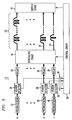
optical packet switch 14. As described above,optical switch 14 includesscheduling stage 16 and switchingstage 18, both coupled byoptical delay lines 20. Switching control typically is performed electronically byelement 30, but optical implementations of the switching control also are within the scope of the invention. In a preferred embodiment,optical packet switch 14 also includes aheader detector 28,control circuit 30, preprocessingcircuitry 32, andconstant delay lines 38. Each of these elements is discussed in detail below in relation to FIG. 6. -
Scheduling stage 16 is an n x m switching module having n inputs and m outputs. Switchingstage 18 is an m x n switching module having m inputs and n outputs.Optical switch 14 typically includes m delay lines. - One performance criterion to be considered for
optical packet switch 14 is the probability of blockage, discussed above. Probability of blockage refers to the probability that a randomly chosen data packet cannot be scheduled on any ofoptical delay lines 20, and consequently is lost. Switch performance increases as the probability of blockage decreases. Probability of blockage can be decreased by increasing the number ofdelay lines 20. FIG. 4 shows the decreasing probability of blockage (Pr(loss)) as a function of input line utilization p, in a switch having 16 inputs, as the number of delay lines m varies from m = 16 to m = 32. Input line utilization is the probability that a delay line contains a data packet in a given time slot. FIG. 4 shows the probability of blockage expressed in log notation as log[Pr(loss)]. -
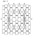
Scheduling stage 16 and switchingstage 18 may be implemented as rearrangeably non-blocking networks. Rearrangeably non-blocking networks have the property that any permutation of the inputs to the network can be achieved at the outputs of the network without blocking (i.e., losing) data. The switching network used to constructscheduling stage 16 and switchingstage 18 may be implemented in a variety of ways. In an exemplary embodiment of the invention, the switching networks ofstages - FIG. 5 illustrates an 8 x 8 Benes network. Benes networks have the property that they permit any of
inputs 31 to be connected to any ofoutputs 33 without blocking provided that no two inputs are to be connected to the same output and thatconnections 35 within the switching fabric can be rearranged. Optical Benes networks suitable for use with the present invention can be constructed as disclosed by Watson et aL, "A Low-Voltage 8 x 8 Ti:LiNbO3 Switch With a Dilated-Benes Architecture," Journal of Lightwave Technology, Vol. 8, No. 5, May 1990, pp. 794-801. - Although the switching networks of
stages -
Optical delay lines 20 typically may be implemented using a single optical fiber for each delay line. Variations in delay from one delay line to the next are achieved by providing optical fibers of increasing length. Assuming all data packet are approximately the same size (i.e., time duration), a one-packet delay line is provided using an optical fiber of predetermined length (the appropriate length of which is readily determinable by one of ordinary skill in the art). Multiple-packet delay lines are implemented by providing optical fibers of a length which is an appropriate multiple of the length of a one-packet delay line. For example, if a one-packet delay is provided by a fiber 1000 meters in length, a two-packet delay line is constructed by providing a fiber 2000 meters in length. Althoughdelay lines 20 typically introduce different amounts of delay, several ofdelay lines 20 may introduce substantially the same predetermined delay. - As discussed with reference to FIG. 3, the data path of
optical packet switch 14 is fully optical, but control within the switch typically is performed electronically. A portion of each optical datapacket entering switch 14 is control information. The control information includes, for example, the destination address of the data packet. This control information is extracted from the optical data packets by aheader detector 28. Each ofheader detectors 28 converts the control information of data packets on its respective input line (see FIG. 3) from the optical domain into the electrical domain.Header detector 28 then routes the converted information (now an electrical signal) to controlcircuit 30 for processing. -
Header detector 28, shown in FIG. 6, includes asplitter 34 and anoptical detector 36.Splitter 34 receives optical data packets from preprocessingcircuitry 32.Splitter 34 splits the optical energy of the incoming data packet into two optical components in a predetermined ratio.Splitter 34 outputs one component α (for use as control information) tooptical detector 36.Splitter 34 outputs a second component 1 - α (for use as data signal) toscheduling stage 16. As shown in FIG. 3, a constantoptical delay line 38 is disposed in series betweensplitter 34 andscheduling stage 16 to introduce a time delay in the passage of the optical data betweenheader detector 28 andscheduling stage 16. The time delay permits the control information to be converted into an electrical signal byoptical detector 36 and to be operated upon by control circuit 30 (e.g., setting the scheduling stage module) before the optical data reachesscheduling stage 16. Splitters suitable for use in accordance with the principles of the invention are commercially- available, for example, from Coming Fibers, Inc. or Gould, Inc. -
Optical detector 36 converts optical signals received fromsplitter 34 into electrical signals. The electrical signals drivecontrol circuit 30. Each ofoptical detectors 36 transmits electrical signals to controlcircuit 30 via a respective one oflines 39. In an illustrative embodiment,optical detector 36 is a low speed detector configured to implement a field coding scheme as disclosed in commonly-owned, co-pending U.S. patent application Serial No. 07/630,145, filed December 19, 1990. The field coding scheme permitsoptical detector 36 to process data at a rate substantially slower than the optical data rate of the transmission system because only the control or header information is processed therein. Detectors suitable for use in accordance with the principles of the invention are commercially available from American Telephone & Telegraph, Inc. -
Control circuit 30 performs three key functions.Control circuit 30 first determines thedelay line 20 to which each data packet arriving atswitch 14 will be connected.Control circuit 30 then sets switches withinscheduling stage 16 to couple the incoming data packet with the appropriate delay line. At the appropriate time,control circuit 30 also sets switches within switchingstage 18 to implement the required switching operation to route the data packet to its desired destination.Control circuit 30 preferably is implemented in hardware because of the high speed required to perform the scheduling operation. - An exemplary embodiment of
control circuit 30 is shown in FIG. 7. The circuit of FIG. 7 is used whenswitch 14 operates in a synchronous mode, with all data packets arriving synchronously atscheduling stage 16. Whilecontrol circuit 30 is described for synchronous switch operation, it is only for illustrative purposes to understand the invention and not for purposes of limitation. In other embodiments,control circuit 30 could control packet scheduling and switching for asynchronous switch operation. In view of the description herein, suitable control circuitry for asynchronous switch operation is deemed apparent to one of ordinary skill in the art. -
Control circuit 30 includes ascanning circuit 37 andseveral stages Control circuit 30 includes a separate stage which corresponds to each column of FIG. 2. However, for discussion purposes, only stages 40, 41, and 42 are shown and described. -
Scanning circuit 37 receives information from each ofheader detectors 28. This information specifies the output (destination) address of each data packet arriving atoptical switch 14.Scanning circuit 37 outputs the output addresses according to scanning techniques such as the techniques discussed above (e.g., sequential or random scanning) to stage 40 for processing. One skilled in the art will readily appreciate that a variety of circuits could be used to implementscanning circuit 37. -
Stage 40 includes alatch 44, aregister 46, andcombinational logic 48.Latch 44 stores output address data received from scanningcircuit 37.Register 46 stores a vector containing the output addresses of all data packets in column m of FIG. 2. The contents oflatch 44 and register 46 are compared incombinational logic 48. The operation ofstage 40 is described below. -
Control circuit 30 includes two system clocks: the clockslot and the clockline. clockslot ticks once every time slot while the clockline ticks at least (n + m) times for every clockslot tick, where n is the number of switch inputs and m is the number ofavailable delay lines 20. The number of delay lines preferably equals or exceeds the number of switch inputs. At every tick of the clockslot a new set of up to n data packets arrive atoptical switch 14.Scanning circuit 37 loads the output address of a single arriving packet intolatch 44 ofcontrol circuit 30 with every tick of the clockline. During the tick of the clockline, the packet destination address is checked against the content ofregister 46. If the contents oflatch 44 indicate a packet destination address already present in register 46 (i.e., two packets are contending for the same switch output in the time slot that corresponds to stage 40), the output ofcombinational logic 48 has a logical value of one. The contents oflatch 44 are then loaded intolatch 50 ofstage 41. If the contents oflatch 44 do not indicate a packet destination address already present in register 46 (i.e., no other packet has been previously scheduled for the same switch output in that time slot), the logical OR of the contents oflatch 44 and register 46 is stored inregister 46. In this way, the data packet described by the contents oflatch 44 is "scheduled" in stage 40 (i.e., it is scheduled in the time slot of column m).Latch 50 is not loaded in this case. - This process continues for all packets arriving within a given time slot. Output addresses of subsequent data packets are loaded sequentially from the scanning circuit into
latch 44. The operation is repeated for each data packet. - Operations performed by
stage 40 are repeated instages stages 41 and 42 (not shown). For example, the contents oflatch 50 are then compared with the contents ofregister 52 ofstage 41. If the contents oflatch 50 indicate a packet destination address already present (i.e., scheduled) inregister 52, the output ofcombinational logic circuitry 54 causes the contents oflatch 50 to be stored inlatch 56 of the next stage. This process is continued until all incoming packets in a given time slot have been analyzed. - Each occurrence of clockslot (corresponding to a new time slot) causes the contents of a given register to be loaded into the next lowest register (i.e., the contents of
register 52 are transferred to register 46, and so on). The contents ofregister 46 can be over-written because the occurrence of a new clockslot indicates that the data packets previously in column m (stage 40) have passed throughdelay lines 20 and have been switched by switchingstage 18.Registers 58 is reset. - In addition to the circuitry described above,
optical packet switch 14 typically may include preprocessingcircuitry 32. Preprocessingcircuitry 32 may include, for example, commercially-available polarization controllers (not shown) for properly polarizing light before the light entersscheduling stage 16. As another example, preprocessingcircuitry 32 may include optical amplifiers (also not shown), which may be desirable in certain instances. For example, if the optical data packets must pass through several switches, some type of optical amplification may be desirable. - Preprocessing
circuitry 32 also may include a synchronization circuit for properly aligning (i.e., synchronizing) the arrival of data packets atscheduling stage 16, for synchronous switch operation. FIG. 8 shows one illustrative embodiment of asuitable synchronization circuit 58.Synchronization circuit 58 includes apacket detector 60,optical switches optical delay lines 70, and acontrol element 72.Optical switches optical delay lines 70. Suitable optical switches are commercially available, for example, from American Telephone & Telegraph, Inc.Optical delay lines 70 are fiber lines of sufficient length to introduce a 0.25 packet delay. -
Synchronization circuit 58 operates as follows. Optical data packets enterpacket detector 60.Packet detector 60 passes most of the optical energy of an entering data packet to switch 62.Packet detector 60 converts the remaining portion of the optical energy into an electrical signal. (In a preferred embodiment, the function ofpacket detector 60 is combined with that ofheader detector 28.) The electrical signal is sent to controlelement 72 vialine 74.Control element 72 determines the delay required to synchronize the incoming packet, and setsswitches Switch 68 outputs the data packet to header detector 28 (see FIG. 3). - It will be understood that the foregoing is merely illustrative of the principles of the invention and not for purposes of limitation. Various modifications can be made by those skilled in the art without departing from the invention. For example, the scheduling technique and control
circuit 30 may be modified to maintain the sequence of data packets arriving atswitch 14. A pointer (or several pointers) is provided to keep track of the packets destined for each output ofswitch 14. The pointer ensures that each data packet destined for a predetermined switch output is placed on a delay line of longer delay than are packets destined for the same output which arrived at the switch earlier in time. Thus, if a packet arrived atswitch 14 for output j and was scheduled on delay line da, a second packet arriving for output j can be scheduled only on delay line db, where db is of longer delay than da.
Claims (16)
- An optical packet switch (14) having a plurality of inputs for receiving optical data packets and a plurality of outputs, comprising:CHARACTERIZED BY:switching means (18) for switching in an optical domain a plurality of optical data packets received at the plurality of inputs to selected ones of the plurality of outputs of the optical packet switch (14);detecting means (28,30) for detecting contentions between ones of the plurality of optical data packets for an output of the optical packet switch (14); andoptical delay line means (16,20,30) for staggering in time, in a feed-forward manner, the plurality of optical data packets so that only one packet is received at the switching means (18) at one time.
- The apparatus of claim 1, wherein the optical delay line means (20) comprises:a plurality of feed-forward optical delay lines (22), at least two of the plurality of optical delay lines (22) being of different delay; andselecting means (30) for selecting ones of the plurality of optical delay lines (22) for transmitting predetermined optical data packets to the switching means (18) so that optical data packets contending for an output of the optical packet switch (14) arrive at the switching means (18) staggered in time.
- The apparatus of claim 2, wherein the selecting means (30) comprises:a switching module (16) having a plurality of switch elements for coupling the plurality of inputs of the optical packet switch (14) with ones of the plurality of optical delay lines;determining means (30) for determining through which of the plurality of optical delay lines (22) each of the optical data packets received at the plurality of inputs shall be transmitted; andsetting means (30) for setting the plurality of switch elements so as to couple ones of the plurality of inputs with ones of the plurality of optical delay lines, the setting means (30) being responsive to the determining means (30).
- The apparatus of claim 1, wherein the detecting means (28) comprises extracting means (34) for extracting from an optical data packet information identifying a predetermined one of a plurality of outputs to which the optical data packet is to be switched.
- The apparatus of claim 2, further comprising coupling means (30) for coupling predetermined ones of the plurality of inputs to selected ones of the plurality of optical delay lines (22) to delay in time arrival of predetermined ones of the optical data packets at the switching means (18) so that contentions between the predetermined optical data packets for ones of the plurality of outputs are resolved, the coupling means (30) being responsive to the detecting means (28).
- The apparatus of claim 5, further comprising synchronizing means (58) for synchronizing arrival of the optical data packets at the plurality of inputs, the synchronizing means (58) being coupled to the plurality of the inputs.
- The apparatus of claim 5, wherein the coupling means (30) comprises:a switching module (16) having a plurality of switches for coupling ones of the plurality of inputs with ones of the plurality of optical delay lines (22);determining means (30) for determining through which of the plurality of optical delay lines (22) the optical data packets received at the plurality of inputs shall be transmitted; andsetting means (30) for setting the plurality of switches so as to couple ones of the plurality of inputs with ones of the plurality of optical delay lines (22), the setting means (30) being responsive to the determining means (30).
- The apparatus of claim 7, wherein the switching means (18) and the switching module (16) comprise a switching fabric network selected from among the group consisting of Benes, Clos, Banyan, Omega, and Shuffle networks.
- The apparatus of claim 7, wherein the determining means (30) further comprises preserving means (30) for preserving packet order of the optical data packets received at the plurality of inputs.
- The apparatus of claim 5, wherein the detecting means (28) comprises extracting means (28) for extracting from an optical data packet information identifying the predetermined one of the plurality of outputs to which the optical data packet is to be switched, the extracting means being coupled to the determining means to provide said information to the determining means.
- The apparatus of claim 7, wherein the determining means (30) operates in a synchronous mode.
- The apparatus of claim 7, wherein the determining means (30) operates in an asynchronous mode.
- A method for switching optical packets within an optical packet switch (14) having a plurality of inputs for receiving optical data packets and a plurality of outputs, comprising the steps of:CHARACTERIZED BY:switching in an optical domain the plurality of optical data packets;detecting contentions between at least two optical data packets destined for the same output of the optical packet switch (14); andcoupling predetermined ones of the plurality of inputs to selected ones of a plurality of optical delay lines (22) of progressively larger feed-forward delay so as to delay in time arrival of predetermined ones of the optical data packets to a switching means so that only one packet is received at a switching means at one time.
- The method of claim 13, further comprising the step of synchronizing arrival of the optical data packets at the plurality of inputs.
- The method of claim 13, wherein the coupling step comprises:determining through which of the plurality of optical delay lines (22) each of the optical data packets received at the plurality of inputs shall be transmitted; andsetting, in response to the determining step, a plurality of switches (18) to couple predetermined ones of the plurality of inputs with predetermined ones of the plurality of optical delay lines (22).
- The method of claim 13, further comprising the step of preserving packet order of the optical data packets received at the plurality of inputs.
Applications Claiming Priority (2)
| Application Number | Priority Date | Filing Date | Title |
|---|---|---|---|
| US807915 | 1985-12-11 | ||
| US80791591A | 1991-12-16 | 1991-12-16 |
Publications (3)
| Publication Number | Publication Date |
|---|---|
| EP0547836A2 EP0547836A2 (en) | 1993-06-23 |
| EP0547836A3 EP0547836A3 (en) | 1994-05-18 |
| EP0547836B1 true EP0547836B1 (en) | 2001-12-19 |
Family
ID=25197421
Family Applications (1)
| Application Number | Title | Priority Date | Filing Date |
|---|---|---|---|
| EP92311260A Expired - Lifetime EP0547836B1 (en) | 1991-12-16 | 1992-12-10 | Optical packet switch |
Country Status (4)
| Country | Link |
|---|---|
| US (1) | US5469284A (en) |
| EP (1) | EP0547836B1 (en) |
| JP (1) | JP2953894B2 (en) |
| DE (1) | DE69232305T2 (en) |
Families Citing this family (49)
| Publication number | Priority date | Publication date | Assignee | Title |
|---|---|---|---|---|
| CA2190859C (en) * | 1994-05-23 | 2002-01-15 | David Cotter | Optical telecommunications network |
| FR2726726A1 (en) * | 1994-11-04 | 1996-05-10 | Guillemot Christian | SWITCH SYSTEM FOR OPTICAL PACKETS |
| GB2300086B (en) * | 1995-04-18 | 1999-08-04 | Northern Telecom Ltd | Switching arrangement |
| US5668653A (en) * | 1995-07-19 | 1997-09-16 | The United States Of America As Represented By The Secretary Of The Navy | High-speed switch for fast routing of data packets |
| EP0790750B1 (en) * | 1996-02-16 | 2005-05-25 | Alcatel | Optical switch with synchronisation |
| KR100233103B1 (en) | 1997-05-27 | 1999-12-01 | 윤종용 | Apparatus and method for optical switch having circulating structure |
| US6486983B1 (en) * | 1999-12-30 | 2002-11-26 | Nortel Networks Limited | Agile optical-core distributed packet switch |
| US6934471B1 (en) * | 1999-06-03 | 2005-08-23 | Avici Systems, Inc. | Photonic switch using time-slot interchange |
| US6810211B1 (en) | 1999-09-08 | 2004-10-26 | Alcatel | Preferred WDM packet-switched router architecture and method for generating same |
| US6721315B1 (en) * | 1999-09-30 | 2004-04-13 | Alcatel | Control architecture in optical burst-switched networks |
| US6819870B1 (en) | 1999-11-02 | 2004-11-16 | Alcatel | All-optical networking optical fiber line delay buffering apparatus and method |
| JP3374174B2 (en) * | 1999-12-15 | 2003-02-04 | 独立行政法人通信総合研究所 | Packet routing method for photonic network and packet router for photonic network |
| US6671256B1 (en) | 2000-02-03 | 2003-12-30 | Alcatel | Data channel reservation in optical burst-switched networks |
| US6426831B1 (en) | 2000-02-29 | 2002-07-30 | Massachusetts Institute Of Technology | EIT based optical switch/wavelength converter |
| US6763192B1 (en) | 2000-03-03 | 2004-07-13 | Alcatel | Integration of all-optical crossconnect functionality in an optical packet switching apparatus |
| US6570694B1 (en) | 2000-03-03 | 2003-05-27 | Alcatel | System and method for low-jitter asynchronous optical regeneration using wavelength sampling |
| EP1162862A2 (en) * | 2000-06-08 | 2001-12-12 | Alcatel | Optical IP switching router architecture |
| US6728212B1 (en) | 2000-06-23 | 2004-04-27 | Alcatel | Asymmetric void filling scheduler with bandwidth grabbing |
| US6690891B1 (en) * | 2000-10-04 | 2004-02-10 | Alcatel | Method for synchronizing optical signals, an optical synchronizing devices and an optical network node therefor |
| US6804255B1 (en) | 2000-10-12 | 2004-10-12 | Alcatel | Hardware implementation of channel scheduling algorithms for optical routers with FDL buffers |
| US6665495B1 (en) * | 2000-10-27 | 2003-12-16 | Yotta Networks, Inc. | Non-blocking, scalable optical router architecture and method for routing optical traffic |
| US20030128987A1 (en) * | 2000-11-08 | 2003-07-10 | Yaron Mayer | System and method for improving the efficiency of routers on the internet and/or cellular networks an/or other networks and alleviating bottlenecks and overloads on the network |
| WO2003060624A2 (en) * | 2001-12-28 | 2003-07-24 | Yaron Mayer | System and method for improving network router efficiency and alleviating network bottlenecks and overloads |
| WO2002039208A2 (en) * | 2000-11-08 | 2002-05-16 | Yaron Mayer | System and method for improving network router efficiency and alleviating network bottlenecks and overloads |
| US6987732B2 (en) * | 2000-12-15 | 2006-01-17 | Tellabs San Jose, Inc. | Apparatus and methods for scheduling packets in a broadband data stream |
| US20020118421A1 (en) * | 2000-12-22 | 2002-08-29 | Yijun Xiong | Channel scheduling in optical routers |
| US7145704B1 (en) | 2003-11-25 | 2006-12-05 | Cheetah Omni, Llc | Optical logic gate based optical router |
| US20020150238A1 (en) * | 2001-02-15 | 2002-10-17 | Mark Peting | Benes fabric for bit level permutations |
| US7426210B1 (en) | 2001-04-03 | 2008-09-16 | Yt Networks Capital, Llc | Port-to-port, non-blocking, scalable optical router architecture and method for routing optical traffic |
| US7190900B1 (en) * | 2001-07-20 | 2007-03-13 | Lighthouse Capital Partners Iv, Lp | System and method for implementing dynamic scheduling of data in a non-blocking all-optical switching network |
| US7106697B1 (en) * | 2001-07-20 | 2006-09-12 | Lighthouse Capital Partners, Iv, Lp | Method for dynamically computing a switching schedule |
| US7218637B1 (en) | 2001-07-20 | 2007-05-15 | Yotta Networks, Llc | System for switching data using dynamic scheduling |
| JP4009946B2 (en) * | 2003-01-16 | 2007-11-21 | 横河電機株式会社 | Optical path control device |
| TWI239156B (en) * | 2003-09-18 | 2005-09-01 | Ind Tech Res Inst | Multi-wavelength optical packet switch system with shared output buffer |
| CN100428660C (en) * | 2004-01-14 | 2008-10-22 | 电子科技大学 | Optical burst exchange node with internal acceleration |
| WO2005081436A1 (en) * | 2004-02-25 | 2005-09-01 | Siemens Aktiengesellschaft | Method and arrangement for combining time-division multiplex signals |
| US20060171386A1 (en) * | 2004-09-01 | 2006-08-03 | Interactic Holdings, Llc | Means and apparatus for a scaleable congestion free switching system with intelligent control III |
| US7512339B2 (en) | 2004-11-30 | 2009-03-31 | Yokogawa Electric Corporation | Optical packet processing apparatus |
| JP4678290B2 (en) * | 2004-11-30 | 2011-04-27 | 横河電機株式会社 | Optical packet processing device |
| KR100675838B1 (en) * | 2004-12-20 | 2007-01-29 | 한국전자통신연구원 | Frame sequence preservation and traffic allocation apparatus and method in multi-channel link and multi-channel transmitter using the same |
| KR100715523B1 (en) * | 2006-02-13 | 2007-05-07 | 한국정보통신대학교 산학협력단 | Apparatus for data burst transmission in optical burst switching networks and a method thereof |
| US7881617B2 (en) * | 2006-02-24 | 2011-02-01 | Cisco Technology, Inc. | Buffering schemes for optical packet processing |
| US7835649B2 (en) * | 2006-02-24 | 2010-11-16 | Cisco Technology, Inc. | Optical data synchronization scheme |
| US8032258B2 (en) * | 2007-12-04 | 2011-10-04 | Ludwig Lester F | Multi-channel chemical transport bus for microfluidic and other applications |
| FR2963999A1 (en) * | 2010-08-19 | 2012-02-24 | France Telecom | METHOD FOR SWITCHING AN OPTICAL DATA STREAM, COMPUTER PROGRAM PRODUCT, STORAGE MEDIUM AND CORRESPONDING NODE. |
| JP2012165267A (en) * | 2011-02-08 | 2012-08-30 | Fujitsu Telecom Networks Ltd | Optical packet switching system and optical packet switching device |
| JP5597591B2 (en) * | 2011-05-12 | 2014-10-01 | 日本電信電話株式会社 | Optical transmission apparatus and optical transmission method |
| CN106464380B (en) * | 2014-04-18 | 2019-09-20 | 华为技术有限公司 | Interconnection system, device and data transmission method |
| US9910470B2 (en) * | 2015-12-16 | 2018-03-06 | Intel Corporation | Controlling telemetry data communication in a processor |
Family Cites Families (16)
| Publication number | Priority date | Publication date | Assignee | Title |
|---|---|---|---|---|
| US3064936A (en) * | 1960-03-21 | 1962-11-20 | Hanau Engineering Company Inc | Solenoid operated valve |
| US3849604A (en) * | 1973-09-28 | 1974-11-19 | Bell Telephone Labor Inc | Time-slot interchanger for time division multiplex system utilizing organ arrays of optical fibers |
| US3838278A (en) * | 1973-09-28 | 1974-09-24 | Bell Telephone Labor Inc | Optical switching network utilizing organ arrays of optical fibers |
| DE3034640A1 (en) * | 1980-09-13 | 1982-05-06 | Philips Patentverwaltung Gmbh, 2000 Hamburg | ARRANGEMENT FOR RECOGNIZING A BINARY WORD |
| JPS6090443A (en) * | 1983-10-24 | 1985-05-21 | Fujikura Ltd | Optical pulse train forming device |
| US4677618A (en) * | 1985-04-04 | 1987-06-30 | International Business Machines Corporation | Method and apparatus for deskewing WDM data transmitted through a dispersive medium |
| JP2595025B2 (en) * | 1988-03-18 | 1997-03-26 | 株式会社日立製作所 | High-speed packet switching equipment using space division type switches |
| JPH01238341A (en) * | 1988-03-18 | 1989-09-22 | Nec Corp | High speed optical bus |
| JPH01256846A (en) * | 1988-04-07 | 1989-10-13 | Nec Corp | Optical packet line concentration and optical packet exchange |
| JPH025663A (en) * | 1988-06-23 | 1990-01-10 | Nec Corp | Optical packet exchange |
| DE68916231T2 (en) * | 1989-03-23 | 1995-02-02 | Ibm | Method and device for multiple access with distributed queues in a communication system. |
| US5122892A (en) * | 1989-05-08 | 1992-06-16 | At&T Bell Laboratories | Space-division switching network having reduced functionality nodes |
| US5065394A (en) * | 1989-08-03 | 1991-11-12 | Pacific Bell | Packet routing switch |
| US5115428A (en) * | 1989-09-05 | 1992-05-19 | The University Of Colorado Foundation, Inc. | Serial array time-slot interchangers |
| US5157654A (en) * | 1990-12-18 | 1992-10-20 | Bell Communications Research, Inc. | Technique for resolving output port contention in a high speed packet switch |
| JP3103181B2 (en) * | 1992-01-07 | 2000-10-23 | 株式会社荏原製作所 | Fast atom beam source |
-
1992
- 1992-12-10 EP EP92311260A patent/EP0547836B1/en not_active Expired - Lifetime
- 1992-12-10 DE DE69232305T patent/DE69232305T2/en not_active Expired - Fee Related
- 1992-12-11 JP JP35242892A patent/JP2953894B2/en not_active Expired - Fee Related
-
1993
- 1993-05-05 US US08/058,999 patent/US5469284A/en not_active Expired - Lifetime
Also Published As
| Publication number | Publication date |
|---|---|
| DE69232305T2 (en) | 2002-07-25 |
| JP2953894B2 (en) | 1999-09-27 |
| EP0547836A2 (en) | 1993-06-23 |
| DE69232305D1 (en) | 2002-01-31 |
| JPH0685844A (en) | 1994-03-25 |
| US5469284A (en) | 1995-11-21 |
| EP0547836A3 (en) | 1994-05-18 |
Similar Documents
| Publication | Publication Date | Title |
|---|---|---|
| EP0547836B1 (en) | Optical packet switch | |
| EP0634854B1 (en) | Controlled-feedback packet switching system | |
| EP0590877B1 (en) | Multistage optical packet distribution network with bypass | |
| US5734486A (en) | Optical packet switching system | |
| EP0590865B1 (en) | Multistage growable optical packet switching arrangement with bypass | |
| US5311345A (en) | Free space optical, growable packet switching arrangement | |
| EP0794683B1 (en) | Optical ATM self-routing switching system with optical copy network | |
| Spring et al. | Photonic 2x2 packet switch with input buffers | |
| US4879712A (en) | Communications switch | |
| CA2022503C (en) | Fast packet and frequency switch | |
| US20060104281A1 (en) | Packet routing | |
| RU2121230C1 (en) | Optical switching device for connecting optical data locations | |
| EP0622004B1 (en) | Optical processing in asynchronous transfer mode network | |
| JPH04838A (en) | Buffer control system | |
| JP2578946B2 (en) | Optical ATM switching system | |
| Chlamtac et al. | Optimal 2/spl times/1 multi-stage optical packet multiplexer | |
| JP3695853B2 (en) | Optical buffer device | |
| JP3461674B2 (en) | Optical packet concentrator | |
| JPH0729390A (en) | Optical buffer memory | |
| Haas | Comparison of feedforward and feedback configurations of the staggering switch architecture | |
| Chlamtac et al. | Toward optical packet-switched network architectures | |
| Su et al. | Self-Routing Optical Switch Using Ring Topology | |
| JPH06164628A (en) | Optical atm switch | |
| Prucnal | Optically-processed Self-Routing for 1D and 2D Photonic Switching Architectures | |
| EP0987916A1 (en) | Method and apparatus for policing of optical ATM cells |
Legal Events
| Date | Code | Title | Description |
|---|---|---|---|
| PUAI | Public reference made under article 153(3) epc to a published international application that has entered the european phase |
Free format text: ORIGINAL CODE: 0009012 |
|
| AK | Designated contracting states |
Kind code of ref document: A2 Designated state(s): DE GB SE |
|
| PUAL | Search report despatched |
Free format text: ORIGINAL CODE: 0009013 |
|
| AK | Designated contracting states |
Kind code of ref document: A3 Designated state(s): DE GB SE |
|
| RAP3 | Party data changed (applicant data changed or rights of an application transferred) |
Owner name: AT&T CORP. |
|
| 17P | Request for examination filed |
Effective date: 19941103 |
|
| RIN1 | Information on inventor provided before grant (corrected) |
Inventor name: HAAS, ZYGMUNT |
|
| 17Q | First examination report despatched |
Effective date: 19970625 |
|
| GRAG | Despatch of communication of intention to grant |
Free format text: ORIGINAL CODE: EPIDOS AGRA |
|
| GRAG | Despatch of communication of intention to grant |
Free format text: ORIGINAL CODE: EPIDOS AGRA |
|
| GRAH | Despatch of communication of intention to grant a patent |
Free format text: ORIGINAL CODE: EPIDOS IGRA |
|
| GRAH | Despatch of communication of intention to grant a patent |
Free format text: ORIGINAL CODE: EPIDOS IGRA |
|
| GRAA | (expected) grant |
Free format text: ORIGINAL CODE: 0009210 |
|
| AK | Designated contracting states |
Kind code of ref document: B1 Designated state(s): DE GB SE |
|
| REG | Reference to a national code |
Ref country code: GB Ref legal event code: IF02 |
|
| REF | Corresponds to: |
Ref document number: 69232305 Country of ref document: DE Date of ref document: 20020131 |
|
| PGFP | Annual fee paid to national office [announced via postgrant information from national office to epo] |
Ref country code: SE Payment date: 20020923 Year of fee payment: 11 |
|
| PLBE | No opposition filed within time limit |
Free format text: ORIGINAL CODE: 0009261 |
|
| STAA | Information on the status of an ep patent application or granted ep patent |
Free format text: STATUS: NO OPPOSITION FILED WITHIN TIME LIMIT |
|
| PGFP | Annual fee paid to national office [announced via postgrant information from national office to epo] |
Ref country code: DE Payment date: 20021205 Year of fee payment: 11 |
|
| 26N | No opposition filed | ||
| PG25 | Lapsed in a contracting state [announced via postgrant information from national office to epo] |
Ref country code: SE Free format text: LAPSE BECAUSE OF NON-PAYMENT OF DUE FEES Effective date: 20031211 |
|
| PG25 | Lapsed in a contracting state [announced via postgrant information from national office to epo] |
Ref country code: DE Free format text: LAPSE BECAUSE OF NON-PAYMENT OF DUE FEES Effective date: 20040701 |
|
| EUG | Se: european patent has lapsed | ||
| PGFP | Annual fee paid to national office [announced via postgrant information from national office to epo] |
Ref country code: GB Payment date: 20071218 Year of fee payment: 16 |
|
| GBPC | Gb: european patent ceased through non-payment of renewal fee |
Effective date: 20081210 |
|
| PG25 | Lapsed in a contracting state [announced via postgrant information from national office to epo] |
Ref country code: GB Free format text: LAPSE BECAUSE OF NON-PAYMENT OF DUE FEES Effective date: 20081210 |