EP0549313A2 - N-bit wide parallel rotation algorithm - Google Patents
N-bit wide parallel rotation algorithm Download PDFInfo
- Publication number
- EP0549313A2 EP0549313A2 EP92311668A EP92311668A EP0549313A2 EP 0549313 A2 EP0549313 A2 EP 0549313A2 EP 92311668 A EP92311668 A EP 92311668A EP 92311668 A EP92311668 A EP 92311668A EP 0549313 A2 EP0549313 A2 EP 0549313A2
- Authority
- EP
- European Patent Office
- Prior art keywords
- bits
- shifter
- buffer means
- image
- word
- Prior art date
- Legal status (The legal status is an assumption and is not a legal conclusion. Google has not performed a legal analysis and makes no representation as to the accuracy of the status listed.)
- Granted
Links
- 239000000872 buffer Substances 0.000 claims abstract description 59
- 230000015654 memory Effects 0.000 abstract description 14
- 238000006243 chemical reaction Methods 0.000 abstract 1
- 238000000034 method Methods 0.000 description 11
- 101100328887 Caenorhabditis elegans col-34 gene Proteins 0.000 description 6
- 238000010586 diagram Methods 0.000 description 3
- 102100031584 Cell division cycle-associated 7-like protein Human genes 0.000 description 1
- 101000777638 Homo sapiens Cell division cycle-associated 7-like protein Proteins 0.000 description 1
- 238000012986 modification Methods 0.000 description 1
- 230000004048 modification Effects 0.000 description 1
Images


Classifications
-
- G—PHYSICS
- G06—COMPUTING; CALCULATING OR COUNTING
- G06T—IMAGE DATA PROCESSING OR GENERATION, IN GENERAL
- G06T3/00—Geometric image transformation in the plane of the image
- G06T3/60—Rotation of a whole image or part thereof
Definitions
- This invention is in the field of digital image data handling, and more specifically is a method of rotating an image by any whole number multiple of ninety degrees.
- Some inventions handle this requirement by the provision of a specially designed memory into which image data words can be written in one direction and read out in an orthogonal direction.
- special purpose memories are expensive, and tend to have a small capacity.
- This prior method can be explained as the rotation of the bits within each 4 by 4 bit block and the rotation of the blocks of the whole image.
- the first word is loaded into the first line of a 4 by 4 bit buffer.
- the next word is circularly rotated one bit and loaded into the second line of the buffer.
- the third word is circularly shifted two bits and loaded into the third line of the buffer and the fourth line is circularly shifted three bits and loaded into the fourth line of the buffer.
- a horizontal line in the original image is still a horizontal line in the buffer, but a vertrical line in the original is now a diagonal line in the buffer.
- any bit in each device is addressable independently of the other devices, and a bit in one word in the buffer can be loaded into any of the four words of memory. Therefore if the bits in the buffer are addressed along diagonal lines parallel to the diagonal line in the buffer and loaded into single words of the memory, the diagonal line in the buffer will become a horizontal line at the output. Thus, the original vertical line is now horizontal. Continuing with addressing the bits along diagonal lines, a horizontal line in the buffer will become a diagonal line at the output. The output four words, prior to storage in memory, are shifted to line up the diagonal bits into a vertical line. Since this line started as a horizontal line, it can be seen that the 4 by 4 bit block has now been completely rotated 90 degrees. To rotate the blocks within the image, a simple addressing algorithm provides that the blocks read out of the block buffer are read into the correct area of a page buffer.
- the above-described method relies on the idea that any one, but only one, bit from each of 4 memory devices can be accessed at one time. Therefore, if four vertical bits in a line are stored in one device, those four bits can never be output all at the same time, and a rotation that requires those bits to be formed into a horizontal line is impossible. However, if the vertical line is converted into a diagonal line (and the horizontal line is left horizontal) then each bit of each line resides in a different device, and the diagonal line, which originally was vertical, can be read out as a horizontal line.
- the above-described method relies on a memory implemented from "by 1" devices, since, as described above, each bit in each device must be independently addressable.
- modern memory devices also include “by 4" devices, which means that every access outputs four bits in parallel, none of which are individually addressable: All four bits must come from the same address. What is required is a method that will perform this rotation in a memory implemented from such "by 4" devices.
- the present invention provides a circuit for rotating an x scanline by y bit image grouped into m-bit words according to claim 1 of the appended claims.
- the process of rotating the image starts with the reception of the image arriving on a data bus.
- An example would be an image that is 256 scanlines by 256 bits coming in, one 16 bit word at a time, on a 16 bit data bus.
- the scanlines are numbered 0, 1, 2, 3, etc.
- the page buffer is fully loaded, the original bottom horizontal edge of the image will still be horizontal in the page buffer, but all vertical lines of the image will now be groups of diagonal lines in the page buffer, one pixel of each vertical line in each horizontal group of 4 bits.
- the bits are read out four 4-bit groups at a time, reordered, shifted again by whole number multiples of 4 bits, and loaded into a 4 scanline band buffer.
- the original vertical lines are still diagonal at this point but are now arranged so that 4 pixels from each original vertical line are in each horizontal group of 4 bits.
- the bits can be read out four 4-bit groups at a time to convert the diagonal lines to horizontal lines. At this point the original vertical lines are horizontal, and the original horizontal lines are diagonal.
- the final step is to do final shifts by whole number multiples of 4 bits to bring the diagonal lines to vertical, and the image is completely rotated. This process will now be discussed in more detail with reference to the following drawings.
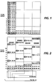
- the image is 16 x 16 bits, and only some of the bits are labelled.
- the labelled bits are line F (in hexadecimal notation) bits 0 to 3, which is written as F L 0, 1, 2, 3 and in the bottom line the labelled bits are line 0, bits 0 to F, written as 0 L 0-F.
- the source of these scanlines is not important, they may be coming from a raster input scanner, a memory, etc.
- the pixels at the left edge of the image are enclosed in circles and the top and bottom lines are enclosed in squares to aid in visualizing the data flow.
- the object of the first operation is to convert the vertical lines of the original image into diagonal lines. This is done by first loading each scanline received into a shifter and shifting each scanline to the right by a number of bits equal to 4 times the scanline number mod 4. Thus, scanline 0 is shifted 0 bits, scanline 1 is shifted 4 bits, scanline 2 is shifted 8 bits, scanline 3 is shifted 12 bits and scanline 4 is shifted 0 bits again. The result is stored into a page buffer implemented from four RAMs, each 4 bits wide, as shown in Fig 2.
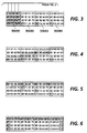
- the next step is to read out from the page buffer along the indicated diagonal.
- the first 16 bit output word is 00, 01, 02, 03, 10, 11, 12, 13, 20, 21, 22, 23, 30, 31, 32, 33. This is reordered by a network of connecting lines that lead to the next shifter. For clarity, only the first four of 16 connecting lines is shown.
- the result is the shifter being loaded by the pattern shown in Fig 3.
- the shifter then shifts to the right by 4 bits times the word number mod 4, and stores the result in the band buffer, resulting in the pattern shown in Fig 4.
- the first 16 bit word read out is 00, 10, 20, 30, 40, 50, 60, 70, 80, 90, A0, B0, C0, D0, E0, F0.
- the shifter the top word is shifted to the left 0 bits, the second word is shifted 4 bits, the third word is shifted 8 bits and the bottom word is shifted 12 bits.
- the result as shown in Fig 6 is output as words of the fully rotated image.
- the scanlines must be stored into the page buffer as shown in Fig 7.
- Each of the sixteen 16-bit words of scanline 0, 0 L 0-F through 0 L FF are circularly shifted 0 bits and loaded into the first 16 addresses as shown.
- the words of each successive scanline up through scanline 7F (hexadecimal for scanline 127) are each circularly shifted 4 bits times the scanline number mod 4, and stored, as shown.
- the result is a fully loaded page buffer, the equivalent of Fig 2.
- the image data bits have to be read out of the page buffer, implemented from RAMs 1, 2, 3 and 4, reordered, shifted and loaded into the four scanline band buffer implemented from the four 4-bit wide RAMs 1', 2', 3'and 4'.
- the first 16 bits of data read from the page buffer RAMs are: 0 L 0, 1, 2, 3 from RAM 1 1 L 0, 1, 2, 3 from RAM 2 2 L 0, 1, 2, 3 from RAM 3 3 L 0, 1, 2, 3 from RAM 4.
- bits will be reordered, shifted 0 bits and stored in the band buffer as follows: 0, 1, 2, 3 L 0 to RAM 1' 0, 1, 2, 3 L 1 to RAM 2' 0, 1, 2, 3 L 2 to RAM 3' 0, 1, 2, 3 L 3 to RAM 4'
- the second 16 bits of data read from the page buffer RAMs are: 4 L 0, 1, 2, 3 from RAM 1 5 L 0, 1, 2, 3 from RAM 2 6 L 0, 1, 2, 3 from RAM 3 7 L 0, 1,2,3 from RAM4
- the data From the band buffer the data will be read out with the proper addressing.
- the first 16 bit word to be read out is: 0, 1, 2, 3 L 0 from RAM 1' 4, 5, 6, 7 L 0 from RAM2' 8, 9, A, B L 0 from RAM3' C, D, E, F L 0 from RAM4'
- the second word to be read out is: 10, 11, 12, 13 L 0 from RAM 1' 14, 15, 16, 17 L 0 from RAM 2' 18, 19, 1A, 1B L 0 from RAM 3' 1C, 1D, 1E, 1F L 0 from RAM 4'
- Fig 9 shows the actual pieces of hardware required for this operation.
- the minimum number of circuit elements required are three shifters, one band buffer and one page buffer.
- two band buffers can be used concurrently, one being loaded while the other is outputing data to the next element.
- This circuit can be used in a number of ways. For example, to rotate an image, it is the designer's choice whether the data flow is upward, into the page buffer first, or downward, into the band buffer first. To get rotations of 90 and 270 degrees, and their mirror images, shifts can be right or left so that diagonals can be formed that proceed upward in either the right or left directions and the store and read cycles can proceed from the bottom or the top of the buffers.
Abstract
Description
- This invention is in the field of digital image data handling, and more specifically is a method of rotating an image by any whole number multiple of ninety degrees.
- It is frequently necessary to rotate an image by 90 or 270 degrees, or to form the mirror image of these. The obvious way to do this is to write an image into a memory in one direction and read it out in the orthogonal direction. For example, sixteen words, each of sixteen bits, could be written into a memory, and then sixteen words could be read out, the first output word containing the first bit of each input word, the second output word containing the second bit of each input word, etc. This is a time consuming process when done in software.
- Some inventions handle this requirement by the provision of a specially designed memory into which image data words can be written in one direction and read out in an orthogonal direction. However, such special purpose memories are expensive, and tend to have a small capacity.
- A method and circuit for producing these rotations at high speed without the necessity of special memory hardware is described in US-A-5,111,192 entitled "Method To Rotate A
Bitmap Image 90 Degrees", andSerial Number 07/721,797, "Parallel Rotation Algorithm", which are incorporated by reference herein. In its simplest form, this prior invention can be described with reference to a 4 by 4 bit block of binary pixels in memory arranged as four horizontal words of four bits each, which must be rotated 90 degrees. - This prior method can be explained as the rotation of the bits within each 4 by 4 bit block and the rotation of the blocks of the whole image. First, the first word is loaded into the first line of a 4 by 4 bit buffer. The next word is circularly rotated one bit and loaded into the second line of the buffer. The third word is circularly shifted two bits and loaded into the third line of the buffer and the fourth line is circularly shifted three bits and loaded into the fourth line of the buffer. At this point a horizontal line in the original image is still a horizontal line in the buffer, but a vertrical line in the original is now a diagonal line in the buffer.
- Since the buffer is implemented from "by 1" devices, any bit in each device is addressable independently of the other devices, and a bit in one word in the buffer can be loaded into any of the four words of memory. Therefore if the bits in the buffer are addressed along diagonal lines parallel to the diagonal line in the buffer and loaded into single words of the memory, the diagonal line in the buffer will become a horizontal line at the output. Thus, the original vertical line is now horizontal. Continuing with addressing the bits along diagonal lines, a horizontal line in the buffer will become a diagonal line at the output. The output four words, prior to storage in memory, are shifted to line up the diagonal bits into a vertical line. Since this line started as a horizontal line, it can be seen that the 4 by 4 bit block has now been completely rotated 90 degrees. To rotate the blocks within the image, a simple addressing algorithm provides that the blocks read out of the block buffer are read into the correct area of a page buffer.
- The above-described method relies on the idea that any one, but only one, bit from each of 4 memory devices can be accessed at one time. Therefore, if four vertical bits in a line are stored in one device, those four bits can never be output all at the same time, and a rotation that requires those bits to be formed into a horizontal line is impossible. However, if the vertical line is converted into a diagonal line (and the horizontal line is left horizontal) then each bit of each line resides in a different device, and the diagonal line, which originally was vertical, can be read out as a horizontal line.
- The above-described method relies on a memory implemented from "by 1" devices, since, as described above, each bit in each device must be independently addressable. However, modern memory devices also include "by 4" devices, which means that every access outputs four bits in parallel, none of which are individually addressable: All four bits must come from the same address. What is required is a method that will perform this rotation in a memory implemented from such "by 4" devices. The present invention provides a circuit for rotating an x scanline by y bit image grouped into m-bit words according to
claim 1 of the appended claims. - The process of rotating the image starts with the reception of the image arriving on a data bus. An example would be an image that is 256 scanlines by 256 bits coming in, one 16 bit word at a time, on a 16 bit data bus. The scanlines are numbered 0, 1, 2, 3, etc. As each word is received, it is shifted in one direction by 4 bits times the
scanline number mod 4, and stored into a page buffer. When the page buffer is fully loaded, the original bottom horizontal edge of the image will still be horizontal in the page buffer, but all vertical lines of the image will now be groups of diagonal lines in the page buffer, one pixel of each vertical line in each horizontal group of 4 bits. - Next, the bits are read out four 4-bit groups at a time, reordered, shifted again by whole number multiples of 4 bits, and loaded into a 4 scanline band buffer. The original vertical lines are still diagonal at this point but are now arranged so that 4 pixels from each original vertical line are in each horizontal group of 4 bits.
- Now, the bits can be read out four 4-bit groups at a time to convert the diagonal lines to horizontal lines. At this point the original vertical lines are horizontal, and the original horizontal lines are diagonal. The final step is to do final shifts by whole number multiples of 4 bits to bring the diagonal lines to vertical, and the image is completely rotated. This process will now be discussed in more detail with reference to the following drawings.
- Embodiments of the present invention will now be described, by way of example, with reference to the accompanying drawings, in which:
- Fig 1 is a diagram of the original simple image;
- Fig 2 is the simple image after the first shift;
- Fig 3 is the simple image data after reordering;
- Fig 4 is the simple image data in the band buffer after the second shift;
- Fig 5 is is the simple image data after it is addressed and output from the band buffer;
- Fig 6 is the fully rotated simple image after the third shift;
- Fig 7 is a larger image as it would be stored in the page buffer;
- Fig 8 is a larger image as it would be arranged in the band buffer;
- Fig 9 is an overall diagram of the circuit; and
- Fig 10 is a diagram of the format of a typical original image.
- The original image is shown in Fig 1. In this simple example, the image is 16 x 16 bits, and only some of the bits are labelled. For example, at the top of the image, the labelled bits are line F (in hexadecimal notation)
bits 0 to 3, which is written asF L line 0,bits 0 to F, written as 0 L 0-F. The source of these scanlines is not important, they may be coming from a raster input scanner, a memory, etc. The pixels at the left edge of the image are enclosed in circles and the top and bottom lines are enclosed in squares to aid in visualizing the data flow. - The object of the first operation is to convert the vertical lines of the original image into diagonal lines. This is done by first loading each scanline received into a shifter and shifting each scanline to the right by a number of bits equal to 4 times the
scanline number mod 4. Thus,scanline 0 is shifted 0 bits,scanline 1 is shifted 4 bits,scanline 2 is shifted 8 bits,scanline 3 is shifted 12 bits andscanline 4 is shifted 0 bits again. The result is stored into a page buffer implemented from four RAMs, each 4 bits wide, as shown in Fig 2. - The next step is to read out from the page buffer along the indicated diagonal. For example, the first 16 bit output word is 00, 01, 02, 03, 10, 11, 12, 13, 20, 21, 22, 23, 30, 31, 32, 33. This is reordered by a network of connecting lines that lead to the next shifter. For clarity, only the first four of 16 connecting lines is shown. The result is the shifter being loaded by the pattern shown in Fig 3. The shifter then shifts to the right by 4 bits times the
word number mod 4, and stores the result in the band buffer, resulting in the pattern shown in Fig 4. - From this second pattern diagonals are again read out and loaded into a shifter as shown in Fig 5. For example, the first 16 bit word read out is 00, 10, 20, 30, 40, 50, 60, 70, 80, 90, A0, B0, C0, D0, E0, F0. In the shifter the top word is shifted to the left 0 bits, the second word is shifted 4 bits, the third word is shifted 8 bits and the bottom word is shifted 12 bits. The result as shown in Fig 6 is output as words of the fully rotated image.
- The example described above is of the rotation of an image that is 16 by 16 bits. However, this method can be scaled up to operate on images of any size. An example of an image that is 128 scanlines by 256 bits follows. The original image is shown in Fig 10.
- First, the scanlines must be stored into the page buffer as shown in Fig 7. Each of the sixteen 16-bit words of
scanline 0, 0 L 0-F through 0 L FF, are circularly shifted 0 bits and loaded into the first 16 addresses as shown. The words of each successive scanline up through scanline 7F (hexadecimal for scanline 127) are each circularly shifted 4 bits times thescanline number mod 4, and stored, as shown. The result is a fully loaded page buffer, the equivalent of Fig 2. - Next, the image data bits have to be read out of the page buffer, implemented from
RAMs
0L RAM 1
1L RAM 2
2L RAM 3
3L RAM 4. - These bits will be reordered, shifted 0 bits and stored in the band buffer as follows:
0, 1, 2, 3L 0 to RAM 1'
0, 1, 2, 3L 1 to RAM 2'
0, 1, 2, 3L 2 to RAM 3'
0, 1, 2, 3L 3 to RAM 4' - The second 16 bits of data read from the page buffer RAMs are:
4L RAM 1
5L RAM 2
6L RAM 3
7L - These bits will be reordered, shifted 4 bits and stored in the band buffer as follows:
4, 5, 6, 7L 3 to RAM 1'
4, 5, 6, 7L 0 to RAM 2'
4, 5, 6, 7L 1 to RAM 3'
4, 5, 6, 7L 2 to RAM 4' - The resultant arrangement of data in the band buffer is shown in Fig 8.
- From the band buffer the data will be read out with the proper addressing. For example, the first 16 bit word to be read out is:
0, 1, 2, 3L 0 from RAM 1'
4, 5, 6, 7L 0 from RAM2'
8, 9, A,B L 0 from RAM3'
C, D, E,F L 0 from RAM4' - The second word to be read out is:
10, 11, 12, 13L 0 from RAM 1'
14, 15, 16, 17L 0 from RAM 2'
18, 19, 1A,1B L 0 from RAM 3'
1C, 1D, 1E,1F L 0 from RAM 4' - These words are then circularly shifted by the appropriate amounts (zero bits for this first scanline) to produce the final output image.
- Fig 9 shows the actual pieces of hardware required for this operation. When arranged in pipeline form, as shown, the minimum number of circuit elements required are three shifters, one band buffer and one page buffer. To speed up the throughput, two band buffers can be used concurrently, one being loaded while the other is outputing data to the next element.
- This circuit can be used in a number of ways. For example, to rotate an image, it is the designer's choice whether the data flow is upward, into the page buffer first, or downward, into the band buffer first. To get rotations of 90 and 270 degrees, and their mirror images, shifts can be right or left so that diagonals can be formed that proceed upward in either the right or left directions and the store and read cycles can proceed from the bottom or the top of the buffers.
- While the invention has been described with reference to a specific embodiment, it will be understood by those skilled in the art that various changes may be made and equivalents may be substituted for elements thereof without departing from the true spirit and scope of the invention. In addition, many modifications may be made without departing from the essential teachings of the invention.
Claims (5)
- A circuit for rotating an x scanline by y bit image grouped into m-bit words comprising:
a first shifter for circularly shifting each word by n bits times the scanline number mod n, where n is a fraction of m,
a page buffer means implemented from n-bit wide memory devices for storing the words shifted by said first shifter,
a system of connecting lines for reordering the output bits of said page buffer means,
a second shifter for receiving and circularly shifting each word received from said connecting lines by n bits times the second shifter word number mod n,
band buffer means implemented from n bit wide memory devices for storing the output of said second shifter, and
a third shifter for receiving and circularly shifting each word received from said band buffer means by n bits times the third shifter scanline number mod n, the result being the fully rotated image. - A circuit for rotating an x scanline by y bit image grouped into 16 bit words comprising:
a first shifter for circularly shifting said each word by n bits times the scanline number, mod n,
band buffer means implemented from n bit wide memory devices for storing the result of said shifting of said first shifter,
a second shifter for receiving and circularly shifting each word received from said band buffer means by n bits times the second shifter word number, mod n,
a system of connecting lines for reordering the output bits of said second shifter,
page buffer means implemented from n bit wide memory devices for storing the output of said connecting lines, and
a third shifter for reading out the image data from said page buffer means and for circularly shifting each word received from said page buffer means by n bits times the third shifter scanline number, mod n, the result being the fully rotated image. - The circuit of Claim 1 or 2 wherein said band buffer means comprises two band buffers in parallel, adapted so that one can be loading data while the other is outputting data.
- The circuit of Claim 1, 2 or 3 wherein said page buffer means comprises two page buffers in parallel, adapted so that one can be loading data while the other is outputting data.
- The circuit of Claim 2 wherein said page buffer means comprises two page buffers in parallel, adapted so that one can be loading data while the other is outputting data.
Applications Claiming Priority (2)
| Application Number | Priority Date | Filing Date | Title |
|---|---|---|---|
| US811865 | 1991-12-23 | ||
| US07/811,865 US5365601A (en) | 1991-12-23 | 1991-12-23 | N-bit wide parallel rotation algorithm |
Publications (3)
| Publication Number | Publication Date |
|---|---|
| EP0549313A2 true EP0549313A2 (en) | 1993-06-30 |
| EP0549313A3 EP0549313A3 (en) | 1993-10-20 |
| EP0549313B1 EP0549313B1 (en) | 1998-05-06 |
Family
ID=25207811
Family Applications (1)
| Application Number | Title | Priority Date | Filing Date |
|---|---|---|---|
| EP92311668A Expired - Lifetime EP0549313B1 (en) | 1991-12-23 | 1992-12-21 | N-bit wide parallel rotation algorithm |
Country Status (4)
| Country | Link |
|---|---|
| US (1) | US5365601A (en) |
| EP (1) | EP0549313B1 (en) |
| JP (1) | JP3074229B2 (en) |
| DE (1) | DE69225390T2 (en) |
Cited By (2)
| Publication number | Priority date | Publication date | Assignee | Title |
|---|---|---|---|---|
| EP0996089A1 (en) * | 1997-01-29 | 2000-04-26 | Nec Corporation | Method and apparatus for rotating image data |
| WO2004057560A1 (en) | 2002-12-20 | 2004-07-08 | Koninklijke Philips Electronics N.V. | Apparatus for re-ordering video data for displays using two transpose steps and storage of intermediate partially re-ordered video data |
Families Citing this family (11)
| Publication number | Priority date | Publication date | Assignee | Title |
|---|---|---|---|---|
| US5450604A (en) * | 1992-12-18 | 1995-09-12 | Xerox Corporation | Data rotation using parallel to serial units that receive data from memory units and rotation buffer that provides rotated data to memory units |
| JP2723056B2 (en) * | 1994-09-29 | 1998-03-09 | 日本電気株式会社 | Data converter |
| US5670982A (en) * | 1995-02-08 | 1997-09-23 | International Business Machines Corporation | System for fast 90-degree rotation of bi-level images |
| US5668980A (en) * | 1995-07-31 | 1997-09-16 | Advanced Micro Devices, Inc. | System for performing rotation of pixel matrices |
| US5870581A (en) * | 1996-12-20 | 1999-02-09 | Oak Technology, Inc. | Method and apparatus for performing concurrent write operations to a single-write-input register file and an accumulator register |
| US5946222A (en) * | 1996-12-20 | 1999-08-31 | Oak Technology, Inc. | Method and apparatus for performing a masked byte addition operation |
| US6223181B1 (en) | 1997-07-31 | 2001-04-24 | Oak Technology, Inc. | Memory conserving and compression technique-compatible image rotation system |
| JP2001069351A (en) * | 1999-08-26 | 2001-03-16 | Matsushita Electric Ind Co Ltd | Picture processor |
| JP5411478B2 (en) * | 2008-10-03 | 2014-02-12 | 古野電気株式会社 | Radar equipment |
| KR101348354B1 (en) * | 2012-05-30 | 2014-01-08 | 주식회사 디에이아이오 | Method of reading page data of nand flash memory device |
| US10365966B1 (en) * | 2014-03-25 | 2019-07-30 | Marvell lnternational Ltd. | Methods and systems for wordline based encoding and decoding in NAND flash |
Citations (3)
| Publication number | Priority date | Publication date | Assignee | Title |
|---|---|---|---|---|
| US4806920A (en) * | 1986-03-28 | 1989-02-21 | Nec Corporation | Device for producing an output image while giving an original image a rotation of 90, 180, or 270 |
| GB2210760A (en) * | 1987-10-05 | 1989-06-14 | Int Computers Ltd | Image rotation circuit |
| EP0433645A2 (en) * | 1989-12-20 | 1991-06-26 | Xerox Corporation | Method to rotate a bitmap image 90 degrees |
Family Cites Families (9)
| Publication number | Priority date | Publication date | Assignee | Title |
|---|---|---|---|---|
| US4271476A (en) * | 1979-07-17 | 1981-06-02 | International Business Machines Corporation | Method and apparatus for rotating the scan format of digital images |
| JPS58159184A (en) * | 1982-03-17 | 1983-09-21 | Nec Corp | Picture turning device |
| US4658430A (en) * | 1984-12-27 | 1987-04-14 | International Business Machines Corp. | System for rotating binary images |
| US4703515A (en) * | 1985-08-26 | 1987-10-27 | Xerox Corporation | Image rotation |
| CA1252902A (en) * | 1985-10-31 | 1989-04-18 | David R. Pruett | Method for rotating a binary image |
| US4797852A (en) * | 1986-02-03 | 1989-01-10 | Intel Corporation | Block shifter for graphics processor |
| DE3713627A1 (en) * | 1986-04-23 | 1987-10-29 | Casio Computer Co Ltd | IMAGE STORAGE CIRCUIT, IN PARTICULAR FOR USE IN ROTATING IMAGE DATA |
| JPH0773920B2 (en) * | 1986-11-17 | 1995-08-09 | 日本電気株式会社 | n × n bit dot matrix 90 ° rotation circuit |
| US5124692A (en) * | 1990-04-13 | 1992-06-23 | Eastman Kodak Company | Method and apparatus for providing rotation of digital image data |
-
1991
- 1991-12-23 US US07/811,865 patent/US5365601A/en not_active Expired - Fee Related
-
1992
- 1992-12-14 JP JP04353514A patent/JP3074229B2/en not_active Expired - Fee Related
- 1992-12-21 EP EP92311668A patent/EP0549313B1/en not_active Expired - Lifetime
- 1992-12-21 DE DE69225390T patent/DE69225390T2/en not_active Expired - Fee Related
Patent Citations (3)
| Publication number | Priority date | Publication date | Assignee | Title |
|---|---|---|---|---|
| US4806920A (en) * | 1986-03-28 | 1989-02-21 | Nec Corporation | Device for producing an output image while giving an original image a rotation of 90, 180, or 270 |
| GB2210760A (en) * | 1987-10-05 | 1989-06-14 | Int Computers Ltd | Image rotation circuit |
| EP0433645A2 (en) * | 1989-12-20 | 1991-06-26 | Xerox Corporation | Method to rotate a bitmap image 90 degrees |
Cited By (2)
| Publication number | Priority date | Publication date | Assignee | Title |
|---|---|---|---|---|
| EP0996089A1 (en) * | 1997-01-29 | 2000-04-26 | Nec Corporation | Method and apparatus for rotating image data |
| WO2004057560A1 (en) | 2002-12-20 | 2004-07-08 | Koninklijke Philips Electronics N.V. | Apparatus for re-ordering video data for displays using two transpose steps and storage of intermediate partially re-ordered video data |
Also Published As
| Publication number | Publication date |
|---|---|
| US5365601A (en) | 1994-11-15 |
| JP3074229B2 (en) | 2000-08-07 |
| EP0549313A3 (en) | 1993-10-20 |
| DE69225390D1 (en) | 1998-06-10 |
| EP0549313B1 (en) | 1998-05-06 |
| DE69225390T2 (en) | 1998-10-08 |
| JPH05282437A (en) | 1993-10-29 |
Similar Documents
| Publication | Publication Date | Title |
|---|---|---|
| US4052699A (en) | High speed real time image transformation | |
| US5111192A (en) | Method to rotate a bitmap image 90 degrees | |
| EP0549313B1 (en) | N-bit wide parallel rotation algorithm | |
| US4929085A (en) | Image data rotation processing method and apparatus therefor | |
| US4627020A (en) | Method for rotating a binary image | |
| EP0221418A2 (en) | Improved method for rotating a binary image | |
| EP0147701B1 (en) | Image rotation method | |
| US5889893A (en) | Method and apparatus for the fast rotation of an image | |
| US5361339A (en) | Circuit for fast page mode addressing of a RAM with multiplexed row and column address lines | |
| JP3166447B2 (en) | Image processing apparatus and image processing method | |
| US5613018A (en) | Page buffer rotator | |
| US4916746A (en) | Image rotation circuit | |
| EP0549309B1 (en) | Address reduction scheme implementing rotation algorithm | |
| EP0549316A2 (en) | Page buffer rotator | |
| US5193203A (en) | System for rearranging sequential data words from an initial order to an arrival order in a predetermined order | |
| JPH028335B2 (en) | ||
| JP2753349B2 (en) | Arbitrary angle rotation image data input / output method, input / output circuit thereof, and electronic file device using the same | |
| JPH061449B2 (en) | Image memory for image editing | |
| JPH028336B2 (en) | ||
| JPS6125192B2 (en) | ||
| JPS58219663A (en) | Picture rotation system | |
| GB2210760A (en) | Image rotation circuit | |
| JP3185278B2 (en) | Orthogonal memory | |
| JPH07122899B2 (en) | High speed rotation circuit | |
| JPS63118886A (en) | Converter for digital image |
Legal Events
| Date | Code | Title | Description |
|---|---|---|---|
| PUAI | Public reference made under article 153(3) epc to a published international application that has entered the european phase |
Free format text: ORIGINAL CODE: 0009012 |
|
| AK | Designated contracting states |
Kind code of ref document: A2 Designated state(s): DE FR GB |
|
| PUAL | Search report despatched |
Free format text: ORIGINAL CODE: 0009013 |
|
| AK | Designated contracting states |
Kind code of ref document: A3 Designated state(s): DE FR GB |
|
| 17P | Request for examination filed |
Effective date: 19940412 |
|
| GRAG | Despatch of communication of intention to grant |
Free format text: ORIGINAL CODE: EPIDOS AGRA |
|
| 17Q | First examination report despatched |
Effective date: 19970711 |
|
| GRAG | Despatch of communication of intention to grant |
Free format text: ORIGINAL CODE: EPIDOS AGRA |
|
| GRAH | Despatch of communication of intention to grant a patent |
Free format text: ORIGINAL CODE: EPIDOS IGRA |
|
| GRAH | Despatch of communication of intention to grant a patent |
Free format text: ORIGINAL CODE: EPIDOS IGRA |
|
| GRAA | (expected) grant |
Free format text: ORIGINAL CODE: 0009210 |
|
| AK | Designated contracting states |
Kind code of ref document: B1 Designated state(s): DE FR GB |
|
| REF | Corresponds to: |
Ref document number: 69225390 Country of ref document: DE Date of ref document: 19980610 |
|
| ET | Fr: translation filed | ||
| PLBE | No opposition filed within time limit |
Free format text: ORIGINAL CODE: 0009261 |
|
| STAA | Information on the status of an ep patent application or granted ep patent |
Free format text: STATUS: NO OPPOSITION FILED WITHIN TIME LIMIT |
|
| 26N | No opposition filed | ||
| REG | Reference to a national code |
Ref country code: GB Ref legal event code: IF02 |
|
| PGFP | Annual fee paid to national office [announced via postgrant information from national office to epo] |
Ref country code: GB Payment date: 20041215 Year of fee payment: 13 |
|
| PGFP | Annual fee paid to national office [announced via postgrant information from national office to epo] |
Ref country code: DE Payment date: 20041216 Year of fee payment: 13 |
|
| PGFP | Annual fee paid to national office [announced via postgrant information from national office to epo] |
Ref country code: FR Payment date: 20050825 Year of fee payment: 14 |
|
| PG25 | Lapsed in a contracting state [announced via postgrant information from national office to epo] |
Ref country code: GB Free format text: LAPSE BECAUSE OF NON-PAYMENT OF DUE FEES Effective date: 20051221 |
|
| PG25 | Lapsed in a contracting state [announced via postgrant information from national office to epo] |
Ref country code: DE Free format text: LAPSE BECAUSE OF NON-PAYMENT OF DUE FEES Effective date: 20060701 |
|
| GBPC | Gb: european patent ceased through non-payment of renewal fee |
Effective date: 20051221 |
|
| REG | Reference to a national code |
Ref country code: FR Ref legal event code: ST Effective date: 20070831 |
|
| PG25 | Lapsed in a contracting state [announced via postgrant information from national office to epo] |
Ref country code: FR Free format text: LAPSE BECAUSE OF NON-PAYMENT OF DUE FEES Effective date: 20070102 |