EP0558339B1 - Charge pump circuit - Google Patents
Charge pump circuit Download PDFInfo
- Publication number
- EP0558339B1 EP0558339B1 EP93301466A EP93301466A EP0558339B1 EP 0558339 B1 EP0558339 B1 EP 0558339B1 EP 93301466 A EP93301466 A EP 93301466A EP 93301466 A EP93301466 A EP 93301466A EP 0558339 B1 EP0558339 B1 EP 0558339B1
- Authority
- EP
- European Patent Office
- Prior art keywords
- capacitor
- electrodes
- voltage
- switches
- charge pump
- Prior art date
- Legal status (The legal status is an assumption and is not a legal conclusion. Google has not performed a legal analysis and makes no representation as to the accuracy of the status listed.)
- Expired - Lifetime
Links
Images

Classifications
-
- H—ELECTRICITY
- H02—GENERATION; CONVERSION OR DISTRIBUTION OF ELECTRIC POWER
- H02M—APPARATUS FOR CONVERSION BETWEEN AC AND AC, BETWEEN AC AND DC, OR BETWEEN DC AND DC, AND FOR USE WITH MAINS OR SIMILAR POWER SUPPLY SYSTEMS; CONVERSION OF DC OR AC INPUT POWER INTO SURGE OUTPUT POWER; CONTROL OR REGULATION THEREOF
- H02M3/00—Conversion of dc power input into dc power output
- H02M3/02—Conversion of dc power input into dc power output without intermediate conversion into ac
- H02M3/04—Conversion of dc power input into dc power output without intermediate conversion into ac by static converters
- H02M3/06—Conversion of dc power input into dc power output without intermediate conversion into ac by static converters using resistors or capacitors, e.g. potential divider
- H02M3/07—Conversion of dc power input into dc power output without intermediate conversion into ac by static converters using resistors or capacitors, e.g. potential divider using capacitors charged and discharged alternately by semiconductor devices with control electrode, e.g. charge pumps
Definitions
- This invention concerns a type of charge pump circuit for boosting the voltage used by a capacitor. More specifically, this invention concerns a type of charge pump circuit appropriate for use in the power source portion within the chip of a semiconductor integrated circuit (referred to as IC hereinafter).
- IC semiconductor integrated circuit
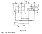
- Figure 10 shows the configuration of a voltage conversion circuit using a conventional charge pump circuit.
- the charge pump circuit comprises capacitors c1, c3, switches s1, s2, s3, s4, oscillator 100 and inverter 102.
- switches s1, s2, s3, s4, switches s1, s3 are set ON/OFF simultaneously by pulse signal pa from oscillator 100 as the switching control signal, while switches s2, s4 are set ON/OFF simultaneously by pulse signal pb from inverter 102.
- pulse signal pa output from oscillator 100 and pulse signal pb output from inverter 102 are opposite in phase, when s1, s3 are turned ON, s2, s4 are turned OFF, and when s1, s3 are turned OFF, s2, s4 are turned ON.
- capacitor c1 is charged to voltage V CC by a power source with an output voltage of V CC through switches s1, s3. Then, as switches s1, s3 are turned OFF and switches s2, s4 are turned ON, capacitor c3 is charged to V CC by the voltage on capacitor c1 through switches s2, s4. As power source voltage V CC is applied to one electrode of capacitor c3, capacitor c3 is charged to V CC , and its electrode on the + side is boosted to a potential of 2V CC . In this way, as the two groups of switches s1,s2, s3,s4 are repeatedly turned ON/OFF alternately and complementarily, a doubled voltage 2V CC , twice the power source voltage V CC , is obtained at output terminal 104.
- Capacitors c2, c4 and switches s5, s6, s7, s8 set in the latter section of the voltage conversion circuit form a polarity inverter for inverting the polarity of voltage 2V CC at output terminal 104.
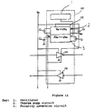
- Figure 11 shows the circuit configuration of a conventional line driver/receiver IC 110 as an example of the method used when the aforementioned voltage conversion circuit is utilized.
- voltage conversion circuit 112 is used to obtain the operating voltage of line driver 114 according to code EIA-232-D by means of a single power source voltage V CC .
- the output voltage V O of the line driver is in the range of +5 V ⁇ V O ⁇ +15 V, -5 V > V O > -15 V.
- +5 V single power source voltage V CC is only supplied as the operation voltage to line receiver 116.
- the power source voltage is changed from 5 V to 3.3 V.
- the line driver/receiver IC 110 shown in Figure 11 since the power source voltage V CC is input as a voltage of 3.3 the line driver output voltages V DD , V SS obtained from voltage conversion circuit 112 are at most +6.6 V and -6.6 V, respectively. This voltage level, however, fails to provide a sufficient margin for the EIA-232-D code.
- the only way to solve this problem is to use the voltage conversion circuit shown in Figure 10 in which another stage of the charge pump circuit is added to form a 2-stage type charge pump circuit.
- the numbers of parts of capacitors c1, c3 and switches sl, s2, s4 are doubled to 4 and 8, respectively.
- capacitors cl, c3 are parts annexed to line driver/receiver IC 110. Consequently, as the number of capacitors is doubled, not only is the reliability of operation degraded, it also becomes difficult to form a small-sized lightweight circuit substrate. Also, as the number of switches sl, s2, s4 is doubled, the IC design becomes more complex, and the cost increases.
- US-A-4 302 804 on which the preambles of claims 1 and 2 are based, shows a charge boost circuit that uses a switching controller in the form of a 4-position sequential counter which operates in a cycle requiring four phases.
- the purpose of this invention is to solve the aforementioned problems of the conventional methods by providing a type of charge pump circuit characterized by the fact that the voltage can be boosted by a factor of 4 or 8 by means of a simple circuit configuration.
- This invention provides a method of operating a charge pump circuit comprising the steps of: coupling a first electrode of a first capacitor via first rectifying means to a first voltage source for providing a prescribed voltage and coupling the second electrode to a reference potential via a first switching means and to said first voltage source via a second switching means; coupling a first electrode of a second capacitor via a second rectifying means to said first electrode of said first capacitor, and coupling the second electrode of said second capacitor via a third switching means to said reference potential and via a fourth switching means to said first electrode of said first capacitor; characterized by generating switching control signals which alternately set said first and second switching means ON/OFF with a prescribed period and which alternately set said third and fourth switching ON/OFF within each period of the prescribed period, and in that the switching frequency of said first and second switching means is half the switching frequency of said third and fourth switching means.
- the invention also provides a charge pump circuit comprising: an input terminal for receiving an input voltage from a power voltage source; a first capacitor having first and second electrodes of opposite polarities, said first capacitor being connected via one of said first and second electrodes to said input terminal; a first rectifying means interposed in the connection between said one of said first and second electrodes of said first capacitor and said input terminal; said first capacitor being connected via the other of said first and second electrodes to said input terminal and to a predetermined reference potential; a first switch interposed in the connection between the other of said first and second electrodes of said first capacitor and said input terminal; a second switch interposed in the connection between the other of said first and second electrodes of said first capacitor and the predetermined reference potential; a second capacitor having first and second electrodes of opposite polarities, said second capacitor being connected via one of said first and second electrodes thereof to said one of said first and second electrodes of said first capacitor; a second rectifying means interposed in the connection between said one of said first and second electrodes of said second capacitor and said one of said
- the first switching means When the first switching means is ON and the second switching means is OFF, the first capacitor is charged to a level between the voltage of the power source and the reference potential via the first rectifying means and the first switch. Then, when the first switching means is turned OFF and the second switching means is turned ON, the other electrode of the first capacitor has its potential clamped; hence, the voltage of one electrode of the first capacitor is boosted to a voltage level equal to the sum of the power source voltage and the charging voltage, and this voltage level can be maintained for a prescribed period.
- the fourth switching means is turned OFF and the third switching means is turned ON; in this case, [the second capacitor] is charged to a voltage between the voltage of the first capacitor and the reference potential via the second rectifying means and the third switch. Then, when the fourth switching means is turned ON and the third switching means is turned OFF, the other electrode of the second capacitor is clamped to the voltage of one electrode of the first capacitor via the fourth switching means, and the voltage obtained on one electrode of the second capacitor is equal to the sum of the charging voltage of the first capacitor and the charging voltage of the second capacitor connected in series.
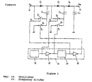
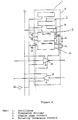
- Figure 1 shows the basic circuit configuration of the charge pump circuit in an embodiment of this invention.
- a prescribed power source voltage V CC is input to input terminal 10
- an output voltage V DD quadrupled power source voltage V CC , 4V CC , is output from output terminal 12.
- the + side electrode is connected via diode D1 to input terminal 10, and the - side electrode is connected via switch S1 to input terminal 10 and via switch S2 to ground potential.
- the anode is connected to the input terminal and the cathode is between input terminal 10 and first capacitor C1 in an appropriate direction to ensure connection to the + side electrode of capacitor C1.
- the two switches S1, S2 are analog switches made of transistor switches; they are turned ON/OFF alternately upon receiving pulse signals PA, PB of opposite phase from switch control circuit 14.
- the + side electrode is connected to the + side electrode of capacitor C1 via diode D2, and the - side electrode is connected via switch S3 to the + side electrode of capacitor C1 and via switch S4 to ground potential.
- the anode is connected to the + side electrode of capacitor C1, and the cathode is inserted between capacitor C1 and capacitor C2 in an appropriate direction to ensure connection to the + side electrode of capacitor C2.
- two switches S3, S4 are analog switches made of transistor switches; they are turned ON/OFF alternately upon receiving pulse signals PC, PD of opposite phase from switch control circuit 14.
- the + side electrode is connected via diode D0 to + side electrode of capacitor C0 and output terminal 12.
- the - side electrode is grounded.
- the anode is connected to the + side electrode of capacitor C2
- the cathode is between capacitor C2 and capacitor C0 in an appropriate direction to ensure connection to the + side electrode of capacitor C0.
- Switch control circuit 14 comprises oscillator 16, inverter 18, frequency divider 20, and inverter 22, which are connected in series.
- the pulse signal with a prescribed frequency output from oscillator 16 has its phase inverted by inverter 18; then, the frequency is divided to 1/2 by frequency divider 20, followed by inversion of phase by means of inverter 22.
- the output pulse of oscillator 16, the output pulse of inverter 18, the output pulse of inverter 18, the output pulse of frequency divider 20, and the output pulse of inverter 22, obtained in this switch control circuit 14 are sent as switch control signals PC, PD, PA, PB to the control terminals of switches S3, S4, S1, and S2, respectively.
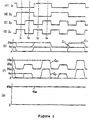
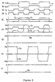
- A, B, C, D show the timing of ON/OFF switching of switches S1, S2, S3, S4, respectively;
- E shows the waveforms of the potential C1+ on the + side electrode of capacitor C1 and the potential C1- on the - side electrode;
- F shows the waveforms of the potential C2+ on the + side electrode of capacitor C2 and the potential C2- on the - side electrode;
- G shows the voltage waveform of output voltage V DD obtained from output terminal 104.
- capacitor C1 is charged to voltage V CC , a voltage between the power source voltage and ground potential, through input terminal 10, diode D1, and switch S2. Consequently, the potential on the + side electrode of capacitor C1 becomes V CC , while the potential of the - side electrode becomes zero.
- capacitor C2 is not charged, and is kept at charging voltage 2V CC .
- the - side electrode of capacitor C2 is connected to ground potential via switch S4; hence, the potential of the + side electrode of capacitor C2 becomes 2V CC .
- capacitors C1, C2 are kept at charging voltages of V CC and 2V CC , respectively, and the + side electrode of capacitor C1 is connected to the - side electrode of capacitor C2 via switch S3. In this way, the potentials of the - side electrode and the + side electrode of capacitor C2 become V CC and 3V CC , respectively.
- the power source voltage V CC is boosted four times, and the quadrupled voltage 4V CC can be obtained periodically.
- voltage 4V CC which is four times the power source voltage V CC , can be output as an almost steady dc voltage V DD .
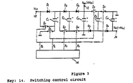
- FIG. 3 shows the circuit configuration of the voltage conversion circuit in an embodiment.
- a polarity inversion circuit is added to the charge pump circuit shown in Figure 1. Consequently, from the output terminal of the charge pump circuit (first output terminal 12), a quadrupled power source voltage V CC 4V CC is output as output voltage V DD , while from the output terminal of the polarity inversion circuit (the second output terminal 24), a negative quadrupled power source voltage V CC -4V CC is output as output voltage V SS .
- the polarity inversion circuit comprises a conventional circuit configuration including capacitors C3, C4, switches S5, S6, diode D3, D4. Switches S5, S6 are turned ON/OFF alternately by using the same switch control signals PA, PB as for switches S1, S2.
- FIG. 5 shows the operation timing or voltage waveforms at the various portions in the voltage conversion circuit.
- A-G show the operation timing or voltage waveforms of the various portions in the charge pump circuit.
- A, B, H, I show the operation timing or voltage waveforms of the various portions in the polarity inversion circuit.
- capacitor C3 is charged to 4V CC by charging voltage 4V CC of output capacitor C0 via switch S5 and diode D3; when switch S5 is OFF and switch S6 is ON, capacitor C4 is charged to 4V CC by the charging voltage 4V CC of capacitor C3 via switch S6 and diode D4. Since the + side electrode of capacitor C4 is connected to ground potential, a negative voltage -4V CC is obtained on the - side electrode of capacitor C4, and this negative voltage -4V CC is output as output voltage V SS from output terminal 24.
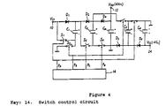
- Figure 4 shows a modified example of the voltage conversion circuit shown by Figure 3.
- the input terminal of the polarity inversion circuit that is, the + side electrode of capacitor C3
- the + side electrode of capacitor C3 is not connected to the + side electrode of output capacitor C0 or output terminal 12; instead, it is connected to the + side electrode of capacitor C2 of the charge pump circuit.
- capacitor C3 since the charging voltage of capacitor C2 is sent to capacitor C3 without going through diode D3, capacitor C3 can be charged effectively, and hence capacitor C4 can be charged effectively without any drop in voltage caused by diode D3.
- FIG. 6 shows an example of the configuration of the line driver/receiver IC using the voltage conversion circuit in this example.
- voltage conversion circuit 32 has the circuit configuration shown in Figure 3 or 4; a positive voltage V DD , 4V CC four times the power source voltage V CC , and negative voltage V SS , -4V CC are output as the operating voltages of line driver 34. Consequently, in this line driver/receiver IC 30, even when the power source voltage V CC is, for example, 3.3 V, it is still able to obtain operating voltages of +13.2 V and -13.2 V by means of voltage conversion circuit 32. Consequently, within a sufficient margin, the standards of EIA-232-D can be met.
- capacitors C0, C1-C4 are annexed to the outside of line driver/receive IC 30.
- the current in line driver/receiver IC 30 is cut off to reduce the power consumption.
- a shutdown signal SD is sent to the various portions within line driver/receiver IC 30.
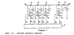
- FIG. 7 shows an embodiment of the circuit configuration of a multistage type charge pump circuit.
- N is an arbitrary positive integer
- a boosting circuit comprising capacitor C1, diode D1, switch SiA, and switch SiB are connected in cascade, and at output terminal 40, a voltage 2 N V CC , which is 2 N times power source voltage V CC .
- switches SiA and SiB are turned ON/OFF alternately by means of switching pulses PiA and PiB of opposite phase from switch control circuit 42.
- the relation between switching pulses PiA, PiB and Pi + 1A, Pi + 1B is that the former PiA, PiB are the 1/2 frequency-divided pulses of the latter Pi + 1A, Pi + 1B.
- one unit of the charge pump circuit comprises a continuous, an arbitrary pair of booster circuits.
- the output voltage of any given charge pump circuit is four times the output voltage of the charge pump circuit of the former stage.
- the input voltage of the charge pump circuit of this invention is not limited to the voltage of the power source; any voltage with a prescribed steady or periodic level by be used as well. Consequently, according to this invention, the power source voltage can be supplied from any circuit that can provide a prescribed steady or periodic voltage.
- FIG 8 shows an embodiment of the circuit configuration of a charge pump circuit used for doubling the negative power source voltage.
- This charge pump circuit has a configuration of the same components as the circuit shown in Figure 1.
- diodes D0, D1, D2 are reversed, compared to those shown in Figure 1; that is, the cathode is connected to the input side, and the anode is connected to the anode side.
- the polarity of the electrodes of capacitors C1, C2, C0 is inverted.
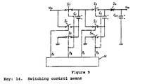
- FIG. 9 shows an embodiment of a charge pump circuit in accordance with this invention in which switches S7, S8 are used instead of diodes D1, D2 as the rectifying means.
- switches S7, S8 may be transistor switches, which are turned ON only during the period when capacitors C1, C2 are charged, since the switches are turned ON/OFF together with switches S2, S4 by means of switching pulses PB, PD.
- the ground potential was set as the reference potential.
- any constant voltage may be used as the reference potential.
Description
respectively. However, as shown in Figure 11, capacitors cl, c3 are parts annexed to line driver/
characterized by generating switching control signals which alternately set said first and second switching means ON/OFF with a prescribed period and which alternately set said third and fourth switching ON/OFF within each period of the prescribed period, and in that the switching frequency of said first and second switching means is half the switching frequency of said third and fourth switching means.
Claims (9)
- A method of operating a charge pump circuit comprising the steps of:characterized by generating switching control signals (PA, PB, PC, PD) which alternately sets said first and second switching means ON/OFF with a prescribed period and which alternately sets said third and fourth switching means ON/OFF within each period of the prescribed period, and in that the switching frequency of said first and second switching means is half the switching frequency of said third and fourth switching means.coupling a first electrode (+) of a first capacitor (C1) via first rectifying means (D1) to a first voltage source (Vcc) for providing a prescribed voltage and coupling the second electrode (-) to a reference potential (GND) via a first switching means (S2) and to said first voltage source via a second switching means (S1);coupling a first electrode (+) of a second capacitor (C2) via a second rectifying means (D2) to said first electrode (+)of said first capacitor (C1), and coupling the second electrode (-) of said second capacitor (C2) via a third switching means (S4) to said reference potential (GND) and via a fourth switching means (S3) to said first electrode (+) of said first capacitor (C1);
- A charge pump circuit comprising:an input terminal (10) for receiving an input voltage from a power voltage source (Vcc);a first capacitor (C1) having first (+) and second (-) electrodes of opposite polarities, said first capacitor being connected via one of said first and second electrodes to said input terminal;a first rectifying means (D1) interposed in the connection between said one of said first (+) and second (-) electrodes of said first capacitor (C1) and said input terminal (10);said first capacitor being connected via the other of said first and second electrodes to said input terminal and to a predetermined reference potential (GND);a first switch interposed (S1) in the connection between the other of said first and second electrodes of said first capacitor and said input terminal;a second switch (S2) interposed in the connection between the other of said first and second electrodes of said first capacitor and the predetermined reference potential (GND);a second capacitor (C2) having first (+) and second (-) electrodes of opposite polarities, said second capacitor being connected via one of said first and second electrodes thereof to said one of said first (+) and second (-) electrodes of said first capacitor (C1);a second rectifying means (D2) interposed in the connection between said one of said first and second electrodes of said second capacitor (C2) and said one of said first and second electrodes of said first capacitor (C1);said second capacitor (C2) being connected via the other of said first and second electrodes thereof to said one electrode of said first and second electrodes of said first capacitor (C1) and to the predetermined reference potential (GND);a third switch (S3) interposed in the connection between the other of said first and second electrodes of said second capacitor and said one electrode of said first and second electrodes of said first capacitor;a fourth switch (S4) interposed in the connection between the other of said first and second electrodes of said second capacitor and the predetermined reference potential (GND), and an outlet terminal (12) connected to the anode of said second diode defining said second rectifying means for producing an output voltage as a power source voltage of significantly boosted magnitude over the input voltage received at said input terminal, characterized by switching control means (14) operably associated with each of said switches for alternately setting said first and second switches ON/OFF within a prescribed time period and alternately setting said third and fourth switches ON/OFF within each period of the prescribed time period and with a switching frequency of said first and second switches being half the switching frequency of said third and fourth switches.
- The charge pump circuit of claim 2 characterized in thatsaid first and second rectifying means respectively comprises first and second rectifying switches operably connected to said switching control means for operation in common with said second and fourth switches in assuming an ON/OFF state in unison with said second and fourth switches respectively and said output terminal is connected to said second rectifying switch.
- The charge pump circuit of claim 2 or 3 characterized in that said switches comprise transistor switches.
- The charge pump circuit of any preceding claim characterized by an output capacitor having first and second electrodes of opposite polarities, said output capacitor being connected via one of said first and second electrodes to said one of said first and second electrodes of said second capacitor and to said output terminal; andan output rectifying means interposed in the connection between said one of said first and second electrodes of said output capacitor and said one of said first and second electrodes of said second capacitor, said output rectifying means comprising a diode having a cathode connected to said one of said first and second electrodes of said second capacitor and an anode connected to said output terminal;said first, second and output rectifying means being connected in series to said output terminal and cooperating to produce a steady-state D.C. voltage of negative potential as the output voltage at said output terminal.
- The charge pump circuit of any preceding claim, characterized in that the switching control means comprises an oscillator.
- The charge pump circuit of claim 6, characterized in that the switching control means further comprises a frequency divider.
- The charge pump circuit of claim 6 or claim 7, characterized in that the switching control means further comprises at least one inverter.
- The charge pump circuit of any preceding claim characterized by additional first and second capacitors connected in parallel to said first and second capacitors to form a chain of N capacitors, where N is greater than 2.
Applications Claiming Priority (2)
| Application Number | Priority Date | Filing Date | Title |
|---|---|---|---|
| JP4076188A JPH05244766A (en) | 1992-02-27 | 1992-02-27 | Charging pump circuit |
| JP76188/92 | 1992-02-27 |
Publications (3)
| Publication Number | Publication Date |
|---|---|
| EP0558339A2 EP0558339A2 (en) | 1993-09-01 |
| EP0558339A3 EP0558339A3 (en) | 1994-04-13 |
| EP0558339B1 true EP0558339B1 (en) | 1998-08-05 |
Family
ID=13598158
Family Applications (1)
| Application Number | Title | Priority Date | Filing Date |
|---|---|---|---|
| EP93301466A Expired - Lifetime EP0558339B1 (en) | 1992-02-27 | 1993-02-26 | Charge pump circuit |
Country Status (4)
| Country | Link |
|---|---|
| US (1) | US5635776A (en) |
| EP (1) | EP0558339B1 (en) |
| JP (1) | JPH05244766A (en) |
| DE (1) | DE69320080T2 (en) |
Families Citing this family (56)
| Publication number | Priority date | Publication date | Assignee | Title |
|---|---|---|---|---|
| US5414669A (en) * | 1993-09-10 | 1995-05-09 | Intel Corporation | Method and apparatus for programming and erasing flash EEPROM memory arrays utilizing a charge pump circuit |
| IT1275104B (en) * | 1994-12-28 | 1997-07-30 | Texas Instruments Italia Spa | "PERFECTED ON-CHIP VOLTAGE MULTIPLIER FOR SEMICONDUCTOR MEMORIES" |
| DE69518826T2 (en) * | 1995-04-14 | 2001-02-22 | St Microelectronics Srl | Voltage step-up circuit for generating an approximately constant voltage level |
| EP0743755A1 (en) * | 1995-05-04 | 1996-11-20 | Siemens Aktiengesellschaft | Integrated circuit |
| US5753841A (en) * | 1995-08-17 | 1998-05-19 | Advanced Micro Devices, Inc. | PC audio system with wavetable cache |
| US6218882B1 (en) * | 1995-12-23 | 2001-04-17 | Nec Corporation | Diode circuit for clamping the signals on a transmission line to a predetermined potential |
| US5808883A (en) * | 1996-02-15 | 1998-09-15 | Harris Corporation | DC-to-DC converter having charge pump and associated methods |
| US5757632A (en) * | 1996-02-29 | 1998-05-26 | Sanyo Electric Co., Ltd. | Switched capacitance voltage multiplier |
| JPH09312968A (en) * | 1996-05-22 | 1997-12-02 | Nec Corp | Charge pump circuit |
| FR2752318B1 (en) * | 1996-08-06 | 1998-09-04 | Inside Technologies | INTEGRATED CIRCUIT WITH NON-CONTACT OPERATION, COMPRISING A LOAD PUMP |
| US6093982A (en) * | 1996-11-15 | 2000-07-25 | Kroll; Mark W. | High voltage output array switching system |
| US5768116A (en) * | 1997-01-27 | 1998-06-16 | Honeywell Inc. | Bi-directional DC/DC voltage converter |
| FR2761214B1 (en) * | 1997-03-19 | 1999-05-21 | Sgs Thomson Microelectronics | CHARGE PUMP TYPE VOLTAGE LIFTING CIRCUIT WITH CONTROLLED NUMBER OF STAGES |
| US6157821A (en) * | 1997-10-23 | 2000-12-05 | Ericsson Inc. | Voltage step up for a low voltage frequency synthesizer architecture |
| KR100605296B1 (en) * | 1998-05-20 | 2006-07-28 | 코닌클리즈케 필립스 일렉트로닉스 엔.브이. | Cascade of voltage multipliers |
| US6021056A (en) * | 1998-12-14 | 2000-02-01 | The Whitaker Corporation | Inverting charge pump |
| US6272029B1 (en) | 1999-02-05 | 2001-08-07 | United Microelectronics Corporation | Dynamic regulation scheme for high speed charge pumps |
| JP2000236657A (en) * | 1999-02-15 | 2000-08-29 | Nec Kyushu Ltd | Booster circuit |
| DE19910015B4 (en) * | 1999-03-08 | 2005-06-30 | Siemens Ag | Method and apparatus for extending the buffer time of a clock circuit |
| US6188274B1 (en) | 1999-06-04 | 2001-02-13 | Sharp Laboratories Of America, Inc. | Bootstrap capacitor power supply for low voltage mobile communications power amplifier |
| US6249446B1 (en) | 2000-08-23 | 2001-06-19 | Intersil Americas Inc. | Cascadable, high efficiency charge pump circuit and related methods |
| DE10045693A1 (en) * | 2000-09-15 | 2002-04-04 | Infineon Technologies Ag | Charge pump circuit |
| DE10050496B4 (en) * | 2000-10-11 | 2015-04-02 | Texas Instruments Deutschland Gmbh | DC converter |
| KR100353538B1 (en) * | 2000-10-24 | 2002-09-27 | 주식회사 하이닉스반도체 | Voltage generator control circuit of semiconductor device |
| US6275395B1 (en) | 2000-12-21 | 2001-08-14 | Micrel, Incorporated | Accelerated turn-off of MOS transistors by bootstrapping |
| US6486728B2 (en) | 2001-03-16 | 2002-11-26 | Matrix Semiconductor, Inc. | Multi-stage charge pump |
| DE10227375A1 (en) | 2002-06-20 | 2004-01-15 | Infineon Technologies Ag | Input voltage increasing method for integrated circuit uses charge pump for pre-charging capacitor and for converting its stored charge to be transferred to output capacitor |
| US6756772B2 (en) | 2002-07-08 | 2004-06-29 | Cogency Semiconductor Inc. | Dual-output direct current voltage converter |
| US6674317B1 (en) | 2002-09-18 | 2004-01-06 | Taiwan Semiconductor Manufacturing Company | Output stage of a charge pump circuit providing relatively stable output voltage without voltage degradation |
| US6738273B2 (en) * | 2002-10-09 | 2004-05-18 | Intersil Americas Inc. | Charge pump drive signal recovery circuit |
| US6985024B2 (en) * | 2003-08-21 | 2006-01-10 | Analog Devices, Inc. | Voltage multiplier |
| TWI250719B (en) * | 2004-04-02 | 2006-03-01 | Au Optronics Corp | DC-DC converter |
| US20050281058A1 (en) * | 2004-06-21 | 2005-12-22 | Issa Batarseh | Dynamic optimization of efficiency using dead time and FET drive control |
| US7855904B2 (en) * | 2005-03-17 | 2010-12-21 | Los Alamos National Security, Llc | Apparatus for producing voltage and current pulses |
| KR100605587B1 (en) | 2005-03-31 | 2006-07-28 | 주식회사 하이닉스반도체 | Semiconductor memory device for internally controlling strength of output-driver |
| KR100716661B1 (en) * | 2005-03-31 | 2007-05-09 | 주식회사 하이닉스반도체 | Voltage booster circuit |
| US7466572B1 (en) * | 2006-04-10 | 2008-12-16 | Marvell International Ltd. | Three phase voltage tripler |
| US8213197B1 (en) * | 2006-09-05 | 2012-07-03 | Marvell International Ltd. | Switching capacitor power supply |
| JP5092924B2 (en) * | 2008-06-19 | 2012-12-05 | 株式会社デンソー | Booster circuit |
| US8897073B2 (en) | 2012-09-14 | 2014-11-25 | Freescale Semiconductor, Inc. | NVM with charge pump and method therefor |
| JP2015211102A (en) * | 2014-04-25 | 2015-11-24 | 株式会社東芝 | Electronic device |
| DE102014210898A1 (en) * | 2014-06-06 | 2015-12-17 | Siemens Aktiengesellschaft | Circuit for a vehicle, in particular a rail vehicle |
| AU2015355241B2 (en) | 2014-12-01 | 2019-10-24 | Pulse Biosciences, Inc. | Nanoelectroablation control and vaccination |
| US9917507B2 (en) | 2015-05-28 | 2018-03-13 | Sandisk Technologies Llc | Dynamic clock period modulation scheme for variable charge pump load currents |
| US9647536B2 (en) | 2015-07-28 | 2017-05-09 | Sandisk Technologies Llc | High voltage generation using low voltage devices |
| US9520776B1 (en) | 2015-09-18 | 2016-12-13 | Sandisk Technologies Llc | Selective body bias for charge pump transfer switches |
| US10548665B2 (en) * | 2016-02-29 | 2020-02-04 | Pulse Biosciences, Inc. | High-voltage analog circuit pulser with feedback control |
| US10874451B2 (en) * | 2016-02-29 | 2020-12-29 | Pulse Biosciences, Inc. | High-voltage analog circuit pulser and pulse generator discharge circuit |
| US10252050B2 (en) | 2016-05-16 | 2019-04-09 | Pulse Biosciences, Inc. | Pulse applicator |
| US10543357B2 (en) | 2016-09-19 | 2020-01-28 | Pulse Biosciences, Inc. | High voltage connectors for pulse generators |
| WO2018151854A1 (en) * | 2017-02-16 | 2018-08-23 | Wispry, Inc. | Charge pump systems, devices, and methods |
| US10946193B2 (en) | 2017-02-28 | 2021-03-16 | Pulse Biosciences, Inc. | Pulse generator with independent panel triggering |
| US10857347B2 (en) | 2017-09-19 | 2020-12-08 | Pulse Biosciences, Inc. | Treatment instrument and high-voltage connectors for robotic surgical system |
| US11571569B2 (en) | 2019-02-15 | 2023-02-07 | Pulse Biosciences, Inc. | High-voltage catheters for sub-microsecond pulsing |
| US11356016B1 (en) * | 2021-03-11 | 2022-06-07 | Infineon Technologies Ag | Multi-stage charge pump circuit |
| US11502619B1 (en) * | 2021-07-30 | 2022-11-15 | Texas Instruments Incorporated | Hybrid multi-level inverter and charge pump |
Family Cites Families (9)
| Publication number | Priority date | Publication date | Assignee | Title |
|---|---|---|---|---|
| US4302804A (en) * | 1979-09-04 | 1981-11-24 | Burroughs Corporation | DC Voltage multiplier using phase-sequenced CMOS switches |
| JPS57110076A (en) * | 1980-12-25 | 1982-07-08 | Mitsubishi Electric Corp | Booster circuit |
| US4451743A (en) * | 1980-12-29 | 1984-05-29 | Citizen Watch Company Limited | DC-to-DC Voltage converter |
| US4812961A (en) * | 1987-05-15 | 1989-03-14 | Linear Technology, Inc. | Charge pump circuitry having low saturation voltage and current-limited switch |
| US4769753A (en) * | 1987-07-02 | 1988-09-06 | Minnesota Mining And Manufacturing Company | Compensated exponential voltage multiplier for electroluminescent displays |
| NL8702734A (en) * | 1987-11-17 | 1989-06-16 | Philips Nv | VOLTAGE MULTIPLICATING CIRCUIT AND rectifying element. |
| US4807104A (en) * | 1988-04-15 | 1989-02-21 | Motorola, Inc. | Voltage multiplying and inverting charge pump |
| JPH04222455A (en) * | 1990-12-20 | 1992-08-12 | Nec Corp | Interface circuit |
| US5237209A (en) * | 1992-03-02 | 1993-08-17 | Analog Devices, Inc. | Bipolar voltage doubler circuit |
-
1992
- 1992-02-27 JP JP4076188A patent/JPH05244766A/en active Pending
-
1993
- 1993-02-26 EP EP93301466A patent/EP0558339B1/en not_active Expired - Lifetime
- 1993-02-26 DE DE69320080T patent/DE69320080T2/en not_active Expired - Fee Related
-
1995
- 1995-03-24 US US08/410,646 patent/US5635776A/en not_active Expired - Lifetime
Also Published As
| Publication number | Publication date |
|---|---|
| DE69320080T2 (en) | 1998-12-10 |
| DE69320080D1 (en) | 1998-09-10 |
| JPH05244766A (en) | 1993-09-21 |
| US5635776A (en) | 1997-06-03 |
| EP0558339A2 (en) | 1993-09-01 |
| EP0558339A3 (en) | 1994-04-13 |
Similar Documents
| Publication | Publication Date | Title |
|---|---|---|
| EP0558339B1 (en) | Charge pump circuit | |
| US5262934A (en) | Bipolar voltage doubler circuit | |
| EP0822478B1 (en) | Voltage converting circuit and multiphase clock generating circuit for driving the same | |
| US7135910B2 (en) | Charge pump with fibonacci number multiplication | |
| US6960955B2 (en) | Charge pump-type booster circuit | |
| US5581455A (en) | Capacitive charge pump, BiCMOS circuit for low supply voltage and method therefor | |
| EP0292148B1 (en) | Charge pump circuitry having low saturation voltage and current-limited switch | |
| US5668703A (en) | Boost converter for driving a capacitive load | |
| US5237209A (en) | Bipolar voltage doubler circuit | |
| US5463283A (en) | Drive circuit for electroluminescent lamp | |
| US4016476A (en) | Booster circuits | |
| US8665255B2 (en) | Power supply circuit and display device including the same | |
| US7071765B2 (en) | Boost clock generation circuit and semiconductor device | |
| US20050012542A1 (en) | Power supply | |
| EP0793333A1 (en) | Charge pump | |
| JP3148070B2 (en) | Voltage conversion circuit | |
| US6605985B2 (en) | High-efficiency power charge pump supplying high DC output currents | |
| US7295198B2 (en) | Voltage booster circuit, power supply circuit, and liquid crystal driver | |
| US11594959B1 (en) | Switched capacitor circuit with passive charge recycling | |
| JP2001004976A (en) | Liquid crystal driving voltage generating circuit | |
| JPH09127912A (en) | Dc boost converter driving capacitive load | |
| US6376934B1 (en) | Voltage waveform generator | |
| JP2002354822A (en) | Switching regulator | |
| JP3345683B2 (en) | Boost circuit | |
| KR100699818B1 (en) | The voltage converter and booster circuit |
Legal Events
| Date | Code | Title | Description |
|---|---|---|---|
| PUAI | Public reference made under article 153(3) epc to a published international application that has entered the european phase |
Free format text: ORIGINAL CODE: 0009012 |
|
| AK | Designated contracting states |
Kind code of ref document: A2 Designated state(s): DE FR GB IT NL |
|
| PUAL | Search report despatched |
Free format text: ORIGINAL CODE: 0009013 |
|
| AK | Designated contracting states |
Kind code of ref document: A3 Designated state(s): DE FR GB IT NL |
|
| 17P | Request for examination filed |
Effective date: 19941010 |
|
| 17Q | First examination report despatched |
Effective date: 19960703 |
|
| GRAG | Despatch of communication of intention to grant |
Free format text: ORIGINAL CODE: EPIDOS AGRA |
|
| GRAG | Despatch of communication of intention to grant |
Free format text: ORIGINAL CODE: EPIDOS AGRA |
|
| GRAH | Despatch of communication of intention to grant a patent |
Free format text: ORIGINAL CODE: EPIDOS IGRA |
|
| GRAH | Despatch of communication of intention to grant a patent |
Free format text: ORIGINAL CODE: EPIDOS IGRA |
|
| GRAA | (expected) grant |
Free format text: ORIGINAL CODE: 0009210 |
|
| ITF | It: translation for a ep patent filed |
Owner name: BARZANO' E ZANARDO ROMA S.P.A. |
|
| AK | Designated contracting states |
Kind code of ref document: B1 Designated state(s): DE FR GB IT NL |
|
| PG25 | Lapsed in a contracting state [announced via postgrant information from national office to epo] |
Ref country code: NL Free format text: LAPSE BECAUSE OF FAILURE TO SUBMIT A TRANSLATION OF THE DESCRIPTION OR TO PAY THE FEE WITHIN THE PRESCRIBED TIME-LIMIT Effective date: 19980805 |
|
| REF | Corresponds to: |
Ref document number: 69320080 Country of ref document: DE Date of ref document: 19980910 |
|
| ET | Fr: translation filed | ||
| NLV1 | Nl: lapsed or annulled due to failure to fulfill the requirements of art. 29p and 29m of the patents act | ||
| PLBE | No opposition filed within time limit |
Free format text: ORIGINAL CODE: 0009261 |
|
| STAA | Information on the status of an ep patent application or granted ep patent |
Free format text: STATUS: NO OPPOSITION FILED WITHIN TIME LIMIT |
|
| 26N | No opposition filed | ||
| REG | Reference to a national code |
Ref country code: GB Ref legal event code: IF02 |
|
| PGFP | Annual fee paid to national office [announced via postgrant information from national office to epo] |
Ref country code: IT Payment date: 20070628 Year of fee payment: 15 |
|
| PGFP | Annual fee paid to national office [announced via postgrant information from national office to epo] |
Ref country code: DE Payment date: 20090227 Year of fee payment: 17 |
|
| PGFP | Annual fee paid to national office [announced via postgrant information from national office to epo] |
Ref country code: GB Payment date: 20090106 Year of fee payment: 17 |
|
| PG25 | Lapsed in a contracting state [announced via postgrant information from national office to epo] |
Ref country code: IT Free format text: LAPSE BECAUSE OF NON-PAYMENT OF DUE FEES Effective date: 20080226 |
|
| PGFP | Annual fee paid to national office [announced via postgrant information from national office to epo] |
Ref country code: FR Payment date: 20090206 Year of fee payment: 17 |
|
| GBPC | Gb: european patent ceased through non-payment of renewal fee |
Effective date: 20100226 |
|
| REG | Reference to a national code |
Ref country code: FR Ref legal event code: ST Effective date: 20101029 |
|
| PG25 | Lapsed in a contracting state [announced via postgrant information from national office to epo] |
Ref country code: FR Free format text: LAPSE BECAUSE OF NON-PAYMENT OF DUE FEES Effective date: 20100301 |
|
| PG25 | Lapsed in a contracting state [announced via postgrant information from national office to epo] |
Ref country code: DE Free format text: LAPSE BECAUSE OF NON-PAYMENT OF DUE FEES Effective date: 20100901 |
|
| PG25 | Lapsed in a contracting state [announced via postgrant information from national office to epo] |
Ref country code: GB Free format text: LAPSE BECAUSE OF NON-PAYMENT OF DUE FEES Effective date: 20100226 |