EP0558770A1 - A hot pluggable electrical circuit - Google Patents
A hot pluggable electrical circuit Download PDFInfo
- Publication number
- EP0558770A1 EP0558770A1 EP92103504A EP92103504A EP0558770A1 EP 0558770 A1 EP0558770 A1 EP 0558770A1 EP 92103504 A EP92103504 A EP 92103504A EP 92103504 A EP92103504 A EP 92103504A EP 0558770 A1 EP0558770 A1 EP 0558770A1
- Authority
- EP
- European Patent Office
- Prior art keywords
- electrical circuit
- port
- signal
- voltage
- net
- Prior art date
- Legal status (The legal status is an assumption and is not a legal conclusion. Google has not performed a legal analysis and makes no representation as to the accuracy of the status listed.)
- Withdrawn
Links
Images
Classifications
-
- G—PHYSICS
- G06—COMPUTING; CALCULATING OR COUNTING
- G06F—ELECTRIC DIGITAL DATA PROCESSING
- G06F13/00—Interconnection of, or transfer of information or other signals between, memories, input/output devices or central processing units
- G06F13/38—Information transfer, e.g. on bus
- G06F13/40—Bus structure
- G06F13/4063—Device-to-bus coupling
- G06F13/4068—Electrical coupling
- G06F13/4081—Live connection to bus, e.g. hot-plugging
-
- H—ELECTRICITY
- H01—ELECTRIC ELEMENTS
- H01R—ELECTRICALLY-CONDUCTIVE CONNECTIONS; STRUCTURAL ASSOCIATIONS OF A PLURALITY OF MUTUALLY-INSULATED ELECTRICAL CONNECTING ELEMENTS; COUPLING DEVICES; CURRENT COLLECTORS
- H01R12/00—Structural associations of a plurality of mutually-insulated electrical connecting elements, specially adapted for printed circuits, e.g. printed circuit boards [PCB], flat or ribbon cables, or like generally planar structures, e.g. terminal strips, terminal blocks; Coupling devices specially adapted for printed circuits, flat or ribbon cables, or like generally planar structures; Terminals specially adapted for contact with, or insertion into, printed circuits, flat or ribbon cables, or like generally planar structures
- H01R12/70—Coupling devices
- H01R12/71—Coupling devices for rigid printing circuits or like structures
- H01R12/72—Coupling devices for rigid printing circuits or like structures coupling with the edge of the rigid printed circuits or like structures
- H01R12/721—Coupling devices for rigid printing circuits or like structures coupling with the edge of the rigid printed circuits or like structures cooperating directly with the edge of the rigid printed circuits
Definitions
- the invention concerns a hot pluggable electrical circuit and in particular a method for hot plugging of an electrical circuit into a separate non-quiesced signal net, such as an active digital or analog bus.
- a method and apparatus for controlled removal and insertion of circuit modules which are interconnected by a bus is known from US-A-4 835 737.
- the operation of the bus is inhibited during the period that a module is being inserted into a connector connected to the bus and the bus is reactivated after the module has been inserted.
- a switch on the module is operated to provide an inhibit signal via the associated connector to a control circuit which inhibits operation of the bus.
- the switch is operated to a second state in which the inhibit signal to the control circuit is reactivated.
- the control circuit again enables the bus to perform normal operations.
- Hot plugging provides both power and data transfer interconnections without causing interruption of ongoing data transfers on the bus.
- Hot plugging is found in fault tolerant systems which normally include device or field replaceable unit redundancy coupled through operational comparison and checking logic to ensure correct operation, see e.g. US-A-4 453 215, US-A-4 486 826, US-A-4 597 084 and US-A-4 654 857.
- a fault is detected an indication of the failing device is provided to service personnel.
- the failing device is then simply removed from the bus and a replacement device connected.
- the removal of the failing device and the replacement of a new device are performed without regard to ongoing bus activity.
- Both the bus architecture and the control device electronics must be carefully designed to achieve this "hot plugging" capability.
- One approach allowed insertion to momentarily impact the bus, but relied on bus error recovery to absorb the transient and maintain system operation, as in US-A-4 453 215. Other designs survive the insertion transients to the point where signal switching was not adversely affected.
- a circuitry for allowing a data cartridge to be hot plugged into an operating terminal without disrupting terminal operation.
- Other circuits are included in this circuitry to isolate the cartridge connector from the address, data and control busses to which it is logically connected.
- the buffer circuits are interposed between the cartridge connector and the busses to avoid bus noise. The buffer is kept in a high impedance state unless the presence of a cartridge has been indicated by an interrupt signal provided directly to the micro processor.
- the active system signal voltage may be high, low, or in transition between these two states. No knowledge of the exact voltage level to be encountered is possible in an active system. Thus connection of a board to an analog or digital bus can occur when the system signals are in any of the states noted above.
- a board in a system typically has a connection interface, some amount of printed circuit board wiring, and eventually a module I/O pin to connect a logic module to the printed circuit board.
- the connector and the printed circuit board etch wiring located above the power plane layers of the board in essence create a capacitor between the printed circuit board etch wiring and ground.
- a module I/O pin also presents some capacitance to ground, and may contain impedances to the supply voltage and to ground as well. Therefore insertion of an electrical circuit, such as a printed circuit board into a non-quiesced signal net instantaneously connects a capacitor load between the signal net and ground.
- the impedance of a capacitor is initially zero when a voltage is first applied to it. Over time as the capacitor accumulates charge, its impedance increases. In the fully charged state, the capacitor presents a very high impedance, in some cases almost infinite. Typically the electrical circuit being plugged has the capacitive load in an uncharged state.
- the fundamental behavior of the capacitor is the reason for the transients seen while inserting electrical circuits into non-quiesced signal nets. So the transient impact of insertion to the active signal net is lessened the lower the switching net voltage, since insertion instantaneously connects the capacitive short circuit to ground. It is observed that the effect is much worse the higher the switching net voltage is. So there is a significant electrical transient in cases where the net voltage is high or in either transition between the high and low states. This transient has to be absorbed or managed by whatever driver devices are actively switching the active system net.
- the present invention has significant benefits in minimizing the electrical transients resulting from insertion of an electrical circuit into a non-quiesced signal net.
- the inventive solution proposes the addition of a preconditioning network to the electrical circuit to be hot plugged to precondition the electrical circuit by partially precharging the input capacitance of the electrical circuit being introduced into a live system. If a first port of a first signal net belonging to the inventive hot pluggable electrical circuit is to be plugged into a second port of a separate non-quiesced second signal net, such as a digital or analog bus, the voltage of said second port can vary between a first and a second limiting value. In order to precondition said first signal net prior to hot plugging, the preconditioning network of the inventive electrical circuit precharges an input capacitance of the first port to be hot plugged to a predefined voltage between said first and said second limiting value.
- Preferably said predefined voltage is set to approximately the arithmetic mean of said first and said second limiting value. However though in some cases it is advantageous to set the predefined voltage to a level below or above the arithmetic mean.
- the predefined voltage can be chosen in consideration of the driver output characteristics of the port into which the electrical circuit is to be hot plugged. If the driver output characteristic is symmetric, the driver can remove as easily charge from the input capacitance of the first port during hot plug as the driver can add charge thereto. In this case the predefined voltage is advantageously set to the arithmetic means of the first and second limiting value.
- the input capacitance which is precharged comprises the cumulative parasitic input capacitance of the first port.
- the port of the inventive hot pluggable electrical circuit which is to be plugged into a port of a separate non-quiesced second signal net comprises at least two terminals, such as ground and a signal line.
- One embodiment of the present invention entails a design of a voltage divider circuit to precharge the parasitic capacitance of the signal net which is to be hot plugged.
- the voltage divider comprises a first impedance to a stable positive power supply voltage and a second impedance to a stable negative power supply voltage.
- the stable positive and negative power supply voltages can be established by making power and ground connections first during board insertion.
- the active signal net is connected later by using some staggered connection means. The relative delay between the two connections can be optimized for applications as needed. Powering up the electrical circuit to be hot plugged before engaging signal nets also assures that electrostatic discharge effects are safely grounded before logic nets are connected. Thereby stable power supply voltages can also be guaranteed before engagement of the signal nets.
- the inventive concept has benefits in minimizing the electrical transients resulting from hot plugging of an electrical circuit into a non-quiesced signal net, such as insertion of a printed circuit board into a non-quiesced analog or digital bus system.
- the concept minimizes the impact of transient effects on a non-quiesced system by addressing the root causes of electrical insertion transients.
- the inventive concept addresses the root causes of electrical insertion transients by minimizing and managing the transient load on the driver of the port of the active system in which the electrical circuit is to be hot plugged.
- the transient load on the driver depends on the initial charge and voltage of the input capacitance of the port of the electrical circuit to be hot plugged. If the voltage of the input capacitance equals the actual driver voltage of the active system in which the port is to be plugged no transient load occurs. If the voltage of the port is at its maximum limiting value - e.g. logic high in a digital system - and the voltage of the input capacitance is zero, a maximum transient load will occur, since in this case the initial impedance of the capacitive load is near zero.
- the voltage of the port is at its minimum limiting value (e.g. logic low) and the voltage of the input capacitance is at its maximum limiting value (e.g. logic high).
- the driver also has to draw a strong current during hot plug, since the capacitance is to be discharged.
- the problem of electrical transients is helped by precharging the input capacitance to a value between the maximum limiting value of the driver output and its minimum limiting value.
- the arithmetic mean of the maximum and minimum limiting values would be an optimal value for the predefined voltage to which the input capacitance is precharged.
- Setting the predefined voltage to the arithmetic mean limits the maximum differential voltage which can occur between the port of the electrical circuit which is to be hot plugged and the corresponding port in the non-quiesced system to half the signal voltage's amplitude.
- the transient load thereby is significantly reduced, since even in the worst case (the voltage of the port of the active system being at either of its limiting values) the differential voltage is only half the signal voltage's amplitude.
- the driver of the port of the active system may have an asymmetric output impedance, so that it can more easily add charge into the input capacitance than remove charge from it or vice versa. In this case it is advantageous to deviate from the theoretical optimal value and to set the predefined voltage to a level below or above the arithmetic mean. Also, the selection of the driver technology (e.g., certain types of CMOS) may dictate a voltage level above or below the arithmetic mean to satisfy electrical interfacing requirements according to the restrictions of specification requirements of DC-voltage levels.
- the invention has value both alone and when used to complement earlier transient management methods, such as methods concerning the management of transients occurring when power or signal connections are hot plugged, the dissipation of electrostatic charges or the dissipation of charge during unplugging.
- the invention provides an economical solution that adapts existing busses to hot plug, since the bus system itself need not necessarily be changed in order to implement the invention. Therefore whether hot pluggable electrical circuits according to the teaching of the invention or circuits not being pluggable are used in an existing bus system merely depends on the customer's choice of design. Further the invention is particularly valuable in a multimedia environment, since multimedia applications demand the frequent exchange of different feature adapters, such as audio jacks or printer port adapters. This can be done on line while processing without powering down the main processing system.
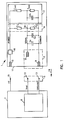
- the only figure shows the connector of an active system 7 having terminals 15, 13, 12 for a stable positive power supply voltage +V, a stable negative power supply voltage (ground) and for a signal voltage V net of the signal net 6 of the active system 7.
- the electrical circuit 1 to be hot plugged is disposed on a printed circuit board and comprises a connection interface 8, 9, 10 for establishing contacts with the terminals 12, 13, 15 of the connector of the active system 7 and the signal line, the common line, and the power line, respectively.
- the power line is connected to an optional unit 16 which generates internal power for the electrical circuit 1 from the externally provided supply voltage +V for those cases in which the internal voltage levels are different than those provided by the active system 7.
- the connection interface 8, 9, 10 comprises staggered connection means.
- the staggered connection means include recessed edge connectors for insertion into the respective terminals of the connector of the active system.
- the connector 8 for the signal line to the signal voltage V net of the active system is recessed from the edge 11 of the board, so that the connections between the common line of the hot pluggable electrical circuit and the ground line of the active system 7 via terminals 9 and 13, as well as the connection between the power line and the stable positive power supply voltage +V via terminals 10 and 15 are made prior to the connection of the signal line to the signal voltage V net of said second signal net via terminals 8 and 12.
- Staggered connection means of this kind are known per se for example from US-A-3 993 935. However, there can be applied any type of connection means which assures that power connections are made prior to signal connection during hot plug.
- the electrical circuit further comprises a signal net, preferably comprising a logic module 2 which is connected via a module I/O pin to the signal line.
- the printed circuit board has several parasitic capacitances: The parasitic capacitance of the connection interface C c , the parasitic capacitance of the printed circuit board edge wiring C e and the parasitic capacitance of the module and its I/O pin C m .
- the total board capacitive load is the sum of all the parasitic capacitances, since they are in parallel.
- the preconditioning network 4 of the inventive hot pluggable electrical circuit shown in the figure comprises two preconditioning impedances Z1 and Z2.
- the impedance Z1 is provided between the power line and the signal line and the impedance Z2 is provided between the signal line and the common line.
- the input impedances Z m1 , Z m2 of the module 2 between the power and signal line and the signal and common line, respectively, are shown in the drawing.
- the impedances Z1, Z m1 and Z2, Z m2 constitute a voltage divider serving to generate a predefined voltage V n to precharge the circuit 1 prior to hot plugging.
- the impedances Z1 and Z2 are connected in parallel to the impedances Z m1 and Z m2 of the module 2.
- the impedances Z m1 and Z m2 normally cannot be changed since Z m1 and Z m2 are fixed circuit parameters of the module 2. These parameters are often given by module manufacturers.
- the impedances Z1 and Z2 are chosen to obtain the desired predefined voltage V n .
- Z1 and Z2 can therefore have a wide variety of values.
- the inventive hot pluggable electrical circuit may comprise additional first ports to be plugged into additional second ports in the active system. If the electrical circuit is to be hot plugged e.g. into an active parallel 64 bit data bus system, there are 64 first ports having 64 signal lines in the electrical circuit.
- the electrical circuit preferably comprises additional impedances to couple the signal lines of the additional first ports to the predefined voltage V n , e.g. by interconnecting the respective signal lines and the voltage V n of the preconditioning network 4 by the additional impedances.
- the resulting impedances of the additional impedances connected to the first and second impedances Z1 and Z2 preferably are large in comparison to an output impedance of said second ports, so that signal transmission will not be significantly influenced by the preconditioning network.
- a drawback of this design is that the signal lines of the first ports are coupled via the additional impedances. It may be required, for example, that a preconditioning network be added to each electrical circuit of every port to be hot plugged, depending on the potential for and the consequence of signal disturbances occurring during hot plug operations.
- the capacitors C c , C e and C m as well as the impedances Z m1 and Z m2 shown in the drawing are merely representations of the equivalent physical circuit of the hot pluggable electrical circuit.
- a first port 3 of a signal net of the electrical circuit is to be preconditioned by the preconditioning network prior to hot plugging into a second port 5 of the active system 7. If the electrical circuit is approached 14 to the connector of the active system, power and ground connections are made first due to the staggered connection interface 8, 9, 10 of the board. Thereby the voltage divider of the preconditioning network precharges the parasitic input capacitance of the first port to a predefined voltage V n , whereby said predefined voltage is preferably set to the arithmetic mean of the limiting values of the signal voltage of the active system. However, other voltages are possible in order to minimize transient effects on the active system.
- the circuit components Z1, Z2 of the preconditioning network as well as the voltage V n can be chosen as follows in order to minimize transient currents and voltages during hot plug.
- the electrical properties of the signal net 6 also depend on the number of electrical circuits, such as feature cards, which are already inserted into the signal net 6.
- the impact of hot plugging an additional electrical circuit into a second port of the signal net 6 can vary in different configurations of the signal net 6. If the signal net 6 comprises for example just one feature card which is already inserted into the signal net, the impact of a hot plugging operation is, generally speaking, more severe than in other configurations where more than one feature card is already inserted in the signal net 6. In the case that the signal net comprises a large number of feature cards the impact of hot plugging is also critical due to the additional load which has to be driven by the active system.
- analog model corresponds to the behavior of the physical circuits in a static operational mode where no hot plugging occurs. If the analog model is sufficiently correlated with the physical reality in the static operational mode it is possible to simulate hot plugging or with other words the dynamic operational mode. For establishing the analog model it is sometimes necessary to readjust the circuit representation of the analog model iteratively, so that it sufficiently corresponds to the actual physical circuit characteristics.
- the invention By partially charging the parasitic capacitances to the predefined voltage V n before the instant of connection of the signal line, these capacitances are no longer short circuits to ground.
- V n By setting the voltage V n to the middle of the switching voltage region of the active system, or somewhat above or below this region, the invention minimizes insertion transient effects on the signal net of the active system. Thereby it is possible to manage the causes of the transient effects.
- the slot may be designed in such a way that either the effect of the insertion speed or the insertion speed itself is reduced.
- the slot design may include staggered connection pin lengths, slot latches, or mechanical means which control the amount of friction during insertion of the electrical circuit to reduce the speed of insertion.
- Another problem is the management of electrostatic discharge during insertion and the removal of residual charges in the electrical circuit capacitances. If the electrical circuit is housed by a mechanical package which is conductive, this can serve for this purpose. The mechanical package usually slides in a conductive guide during insertion of the electrical circuit into the slot. If this guide is connected to the ground of the mechanical assembly, electrostatic charges are thereby removed without causing any damage.
- the design of the mechanical package is important in that it can prevent, for example, short circuiting with other hot pluggable electrical circuits which could result in system malfunctions.
- the design is also important in satisfying operator safety requirements.
- a DC/DC regulator 16 in the figure, can serve to control the inrush current so that overloading is prevented and the electrical circuit is nevertheless powered up at an acceptably quick rate. Such a regulator can also serve to limit the impact of a short circuit in the electrical circuit due to the galvanic isolation of the electrical circuit from the active system. Thus no excessive current is drawn from the electrical circuit if a short circuit should occur.
- a DC/DC regulator also allows an external power source to be attached to the active system such as an external power supply or battery backup unit. This also serves to isolate faults and thus prevent system failure.
- inventive concept can be beneficially applied to both analog and digital systems.
- digital systems the digital switching behavior of the system during board insertion and removal is preserved.
- analog systems the signal distortion of the analog bus is minimized during hot plug by applying the inventive concept.
- the simple impedances Z1 and Z2 in the figure describing the preferred embodiment, may be replaced by more complex circuitry which can also serve to add or subtract charge for the signal net which is being precharged.
- a more complex circuitry may comprise active components such as transistors and/or passive components such as impedances and/or diodes.
- Such networks may or may not operate in response to control signals derived from a staggered or sequential connection means. They may be included within the logic module attached to the signal net 2 or remain as a separate preconditioning network 4 as shown in the figure. These networks can also be designed to generate a predefined precharge voltage V n in accordance with the teaching of this invention.
Abstract
The invention is related to hot plugging of an electrical circuit (1) into a separate non-quiesced signal net (6) in an active system (7), such as a digital or analog bus. The inventive solution proposes the addition of a preconditioning network (4) to precondition the electrical circuit (1) to be hot plugged by partially precharging the parasitic input capacitances (Cc, Ce, Cm) of the electrical circuit (1) before hot plugging. The precharging of the parasitic input capacitances serves to minimize transient effects on the active system (7).
Description
- The invention concerns a hot pluggable electrical circuit and in particular a method for hot plugging of an electrical circuit into a separate non-quiesced signal net, such as an active digital or analog bus.
- Various apparatus and methods for the rapid interconnection of electrical circuits, such as peripheral device interfaces or control circuits to computer busses, are known in the art. In a method to minimize the impact of plugging into a digital bus, the normal procedure has been to disable the bus so that new devices would not disrupt data flow on the bus.
- A method and apparatus for controlled removal and insertion of circuit modules which are interconnected by a bus is known from US-A-4 835 737. According to the teaching of this document, the operation of the bus is inhibited during the period that a module is being inserted into a connector connected to the bus and the bus is reactivated after the module has been inserted. When a module is to be inserted in an associated connector, a switch on the module is operated to provide an inhibit signal via the associated connector to a control circuit which inhibits operation of the bus. Upon full insertion of the module in the associated connector, the switch is operated to a second state in which the inhibit signal to the control circuit is reactivated. As a consequence, the control circuit again enables the bus to perform normal operations. However quiescing of the bus during the insertion period has serious disadvantages other than performance problems, since there is no graceful way to manage peripherals or I/O during the quiesce interruption. Also, since parts of a digital system are asynchronous with respect to each other, logical or sequential operation errors are possible. A digital or analog system is interrupted for many cycles because the mechanical insertion of a board is a relatively slow and imprecise event. Therefore communication or peripheral flow control problems could result in overruns or underruns. As the speed of information transfers increases with the advance of technology, the impact of quiescing the bus during hot plugging becomes more and more severe.
- In contrast the hot plugging concept provides both power and data transfer interconnections without causing interruption of ongoing data transfers on the bus. Hot plugging is found in fault tolerant systems which normally include device or field replaceable unit redundancy coupled through operational comparison and checking logic to ensure correct operation, see e.g. US-A-4 453 215, US-A-4 486 826, US-A-4 597 084 and US-A-4 654 857. When a fault is detected an indication of the failing device is provided to service personnel. The failing device is then simply removed from the bus and a replacement device connected. The removal of the failing device and the replacement of a new device are performed without regard to ongoing bus activity. Both the bus architecture and the control device electronics must be carefully designed to achieve this "hot plugging" capability. One approach allowed insertion to momentarily impact the bus, but relied on bus error recovery to absorb the transient and maintain system operation, as in US-A-4 453 215. Other designs survive the insertion transients to the point where signal switching was not adversely affected.
- From IBM Technical Disclosure Bulletin, Volume 29, No. 7, December 1986, page 2877, a circuitry is known for allowing a data cartridge to be hot plugged into an operating terminal without disrupting terminal operation. Other circuits are included in this circuitry to isolate the cartridge connector from the address, data and control busses to which it is logically connected. The buffer circuits are interposed between the cartridge connector and the busses to avoid bus noise. The buffer is kept in a high impedance state unless the presence of a cartridge has been indicated by an interrupt signal provided directly to the micro processor.
- Other known prior art approaches (US-A-4 750 177 and US-A-4 866 604) required split resistive terminations on the system to terminate the bus and allow faster switching. This was placed on the common printed circuit board that houses the board connectors. It also served to ensure system voltage levels without any system boards present. High current sink drivers/receivers were required, and special layout considerations and limitations were required for this concept to work. The system used overpowered drivers/ receivers in conjunction with the split terminations to "harden" the digital system so that it could withstand the insertion transients. Another known prior art design sought to minimize the impact and terminate the digital net by using a series resistor on the board to be inserted. The value must be carefully chosen to allow hot plug while not effecting the switching characteristics. The main disadvantages are signal delay and the loss of signal voltage across the resistor. These systems had to be carefully designed from the beginning so that hot plugging could work reliably. This becomes increasingly difficult as the bus cycle times decrease and logic speeds increase. In this environment it becomes much more challenging to design a system that can sustain processing and support hot plug. Therefore existing digital or analog systems could not easily be adapted for hot plugging.
- It is therefore an object of the present invention to provide an improved hot pluggable circuit.
- This and other objects are advantageously solved by applying the features laid down in the independent claims. Advantageous embodiments of the present invention are set out in the dependent claims.
- When an electrical circuit such as a printed circuit board is inserted live into a signal net of an analog or digital system, the active system signal voltage may be high, low, or in transition between these two states. No knowledge of the exact voltage level to be encountered is possible in an active system. Thus connection of a board to an analog or digital bus can occur when the system signals are in any of the states noted above.
- A board in a system typically has a connection interface, some amount of printed circuit board wiring, and eventually a module I/O pin to connect a logic module to the printed circuit board. The connector and the printed circuit board etch wiring located above the power plane layers of the board in essence create a capacitor between the printed circuit board etch wiring and ground. A module I/O pin also presents some capacitance to ground, and may contain impedances to the supply voltage and to ground as well. Therefore insertion of an electrical circuit, such as a printed circuit board into a non-quiesced signal net instantaneously connects a capacitor load between the signal net and ground.
- The impedance of a capacitor is initially zero when a voltage is first applied to it. Over time as the capacitor accumulates charge, its impedance increases. In the fully charged state, the capacitor presents a very high impedance, in some cases almost infinite. Typically the electrical circuit being plugged has the capacitive load in an uncharged state. The fundamental behavior of the capacitor is the reason for the transients seen while inserting electrical circuits into non-quiesced signal nets. So the transient impact of insertion to the active signal net is lessened the lower the switching net voltage, since insertion instantaneously connects the capacitive short circuit to ground. It is observed that the effect is much worse the higher the switching net voltage is. So there is a significant electrical transient in cases where the net voltage is high or in either transition between the high and low states. This transient has to be absorbed or managed by whatever driver devices are actively switching the active system net.
- The present invention has significant benefits in minimizing the electrical transients resulting from insertion of an electrical circuit into a non-quiesced signal net.
- The inventive solution proposes the addition of a preconditioning network to the electrical circuit to be hot plugged to precondition the electrical circuit by partially precharging the input capacitance of the electrical circuit being introduced into a live system. If a first port of a first signal net belonging to the inventive hot pluggable electrical circuit is to be plugged into a second port of a separate non-quiesced second signal net, such as a digital or analog bus, the voltage of said second port can vary between a first and a second limiting value. In order to precondition said first signal net prior to hot plugging, the preconditioning network of the inventive electrical circuit precharges an input capacitance of the first port to be hot plugged to a predefined voltage between said first and said second limiting value. Preferably said predefined voltage is set to approximately the arithmetic mean of said first and said second limiting value. However though in some cases it is advantageous to set the predefined voltage to a level below or above the arithmetic mean. The predefined voltage can be chosen in consideration of the driver output characteristics of the port into which the electrical circuit is to be hot plugged. If the driver output characteristic is symmetric, the driver can remove as easily charge from the input capacitance of the first port during hot plug as the driver can add charge thereto. In this case the predefined voltage is advantageously set to the arithmetic means of the first and second limiting value. If the driver output characteristic is asymmetric, the situation is different: For a driver which can more easily add charge than remove charge, a predefined voltage below the arithmetic mean is advantageous. In the opposite case - a driver which can more easily remove charge than add charge - a predefined voltage above the arithmetic mean is advantageous. The input capacitance which is precharged comprises the cumulative parasitic input capacitance of the first port. According to a preferred embodiment of the invention the port of the inventive hot pluggable electrical circuit which is to be plugged into a port of a separate non-quiesced second signal net comprises at least two terminals, such as ground and a signal line.
- One embodiment of the present invention entails a design of a voltage divider circuit to precharge the parasitic capacitance of the signal net which is to be hot plugged. The voltage divider comprises a first impedance to a stable positive power supply voltage and a second impedance to a stable negative power supply voltage. The stable positive and negative power supply voltages can be established by making power and ground connections first during board insertion. The active signal net is connected later by using some staggered connection means. The relative delay between the two connections can be optimized for applications as needed. Powering up the electrical circuit to be hot plugged before engaging signal nets also assures that electrostatic discharge effects are safely grounded before logic nets are connected. Thereby stable power supply voltages can also be guaranteed before engagement of the signal nets. This eliminates the latch up exposure if CMOS logic is used on the inserted board, especially since nets can be precharged to the voltage desired. By connecting signal nets last, there is no need to use drivers or receivers that power on or off glitch free to maintain signal integrity. If power supply voltages are provided to the electrical circuit before signal nets are connected, the drivers or receivers of the electrical circuit which is to be hot plugged are already powered up, when the signal nets of the electrical circuit finally are connected. This is advantageous in that a randomly floating output during powering up of the electrical circuit cannot disturb the non-quiesced second signal net. Moreover, this is advantageous in that a correct power on reset can be applied to the electrical circuit before the connection of the signal nets is established.
- The inventive concept has benefits in minimizing the electrical transients resulting from hot plugging of an electrical circuit into a non-quiesced signal net, such as insertion of a printed circuit board into a non-quiesced analog or digital bus system. The concept minimizes the impact of transient effects on a non-quiesced system by addressing the root causes of electrical insertion transients.
- The inventive concept addresses the root causes of electrical insertion transients by minimizing and managing the transient load on the driver of the port of the active system in which the electrical circuit is to be hot plugged. The transient load on the driver depends on the initial charge and voltage of the input capacitance of the port of the electrical circuit to be hot plugged. If the voltage of the input capacitance equals the actual driver voltage of the active system in which the port is to be plugged no transient load occurs. If the voltage of the port is at its maximum limiting value - e.g. logic high in a digital system - and the voltage of the input capacitance is zero, a maximum transient load will occur, since in this case the initial impedance of the capacitive load is near zero. In the opposite case the voltage of the port is at its minimum limiting value (e.g. logic low) and the voltage of the input capacitance is at its maximum limiting value (e.g. logic high). Thus, in this case the driver also has to draw a strong current during hot plug, since the capacitance is to be discharged. According to the inventive concept the problem of electrical transients is helped by precharging the input capacitance to a value between the maximum limiting value of the driver output and its minimum limiting value.
- In theory the arithmetic mean of the maximum and minimum limiting values would be an optimal value for the predefined voltage to which the input capacitance is precharged. Setting the predefined voltage to the arithmetic mean limits the maximum differential voltage which can occur between the port of the electrical circuit which is to be hot plugged and the corresponding port in the non-quiesced system to half the signal voltage's amplitude. Thus the transient load thereby is significantly reduced, since even in the worst case (the voltage of the port of the active system being at either of its limiting values) the differential voltage is only half the signal voltage's amplitude.
- In practice however, the driver of the port of the active system may have an asymmetric output impedance, so that it can more easily add charge into the input capacitance than remove charge from it or vice versa. In this case it is advantageous to deviate from the theoretical optimal value and to set the predefined voltage to a level below or above the arithmetic mean. Also, the selection of the driver technology (e.g., certain types of CMOS) may dictate a voltage level above or below the arithmetic mean to satisfy electrical interfacing requirements according to the restrictions of specification requirements of DC-voltage levels.
- The invention has value both alone and when used to complement earlier transient management methods, such as methods concerning the management of transients occurring when power or signal connections are hot plugged, the dissipation of electrostatic charges or the dissipation of charge during unplugging. The invention provides an economical solution that adapts existing busses to hot plug, since the bus system itself need not necessarily be changed in order to implement the invention. Therefore whether hot pluggable electrical circuits according to the teaching of the invention or circuits not being pluggable are used in an existing bus system merely depends on the customer's choice of design. Further the invention is particularly valuable in a multimedia environment, since multimedia applications demand the frequent exchange of different feature adapters, such as audio jacks or printer port adapters. This can be done on line while processing without powering down the main processing system.
- An advantageous embodiment of the invention is subsequently described in connection with the drawing in which the only figure is a schematic diagram of an inventive hot pluggable electrical circuit and the signal net in which the circuit is to be hot plugged.
- The only figure shows the connector of an active system 7 having
terminals signal net 6 of the active system 7. Theelectrical circuit 1 to be hot plugged is disposed on a printed circuit board and comprises aconnection interface terminals optional unit 16 which generates internal power for theelectrical circuit 1 from the externally provided supply voltage +V for those cases in which the internal voltage levels are different than those provided by the active system 7. Theconnection interface connector 8 for the signal line to the signal voltage Vnet of the active system is recessed from theedge 11 of the board, so that the connections between the common line of the hot pluggable electrical circuit and the ground line of the active system 7 viaterminals terminals terminals 8 and 12. Staggered connection means of this kind are known per se for example from US-A-3 993 935. However, there can be applied any type of connection means which assures that power connections are made prior to signal connection during hot plug. - The electrical circuit further comprises a signal net, preferably comprising a
logic module 2 which is connected via a module I/O pin to the signal line. Thus, the printed circuit board has several parasitic capacitances: The parasitic capacitance of the connection interface Cc, the parasitic capacitance of the printed circuit board edge wiring Ce and the parasitic capacitance of the module and its I/O pin Cm. The total board capacitive load is the sum of all the parasitic capacitances, since they are in parallel. - The preconditioning network 4 of the inventive hot pluggable electrical circuit shown in the figure comprises two preconditioning impedances Z₁ and Z₂. The impedance Z₁ is provided between the power line and the signal line and the impedance Z₂ is provided between the signal line and the common line. Further the input impedances Zm1, Zm2 of the
module 2 between the power and signal line and the signal and common line, respectively, are shown in the drawing. The impedances Z₁, Zm1 and Z₂, Zm2 constitute a voltage divider serving to generate a predefined voltage Vn to precharge thecircuit 1 prior to hot plugging. In this preferred embodiment the impedances Z₁ and Z₂ are connected in parallel to the impedances Zm1 and Zm2 of themodule 2. The impedances Zm1 and Zm2 normally cannot be changed since Zm1 and Zm2 are fixed circuit parameters of themodule 2. These parameters are often given by module manufacturers. Thus in this case the impedances Z₁ and Z₂ are chosen to obtain the desired predefined voltage Vn. Depending on the values of Zm1 and Zm2, Z₁ and Z₂ can therefore have a wide variety of values. It is however advantageous to choose the values of Z₁ and Z₂ so that the resulting impedances of Z₁ connected in parallel to Zm1 and Z₂ connected in parallel to Zm2 are large in comparison to the output impedance of the port of the active system in which the circuit is to be plugged in. In some cases it is also possible to leave out Z₁ and/or Z₂ or in other words to make them infinitely large, if the values of Zm1 and/or Zm2 already contribute to the desired predefined voltage which is to be generated by the preconditioning network. In order to prevent short circuiting of the impedance Z₁ and/or Z₂, the logic module should be in a high impedance mode during hot plug. - When the connection of the signal line and the signal voltage is established sometimes bouncing of the corresponding contacts occurs. Therefore it is advantageous to choose Z₁ and Z₂ in consideration of the average time interval of bouncing being normally in the range of several milliseconds. If the values of Z₁ and Z₂ are chosen so that the RC-time constants of the preconditioning network are significantly smaller than the average time interval of bouncing, the correct predefined preconditioning voltage Vn is generated before the contacts are finally established, despite the bouncing of the contacts.
- The inventive hot pluggable electrical circuit may comprise additional first ports to be plugged into additional second ports in the active system. If the electrical circuit is to be hot plugged e.g. into an active parallel 64 bit data bus system, there are 64 first ports having 64 signal lines in the electrical circuit. In this case the electrical circuit preferably comprises additional impedances to couple the signal lines of the additional first ports to the predefined voltage Vn, e.g. by interconnecting the respective signal lines and the voltage Vn of the preconditioning network 4 by the additional impedances. The resulting impedances of the additional impedances connected to the first and second impedances Z₁ and Z₂ preferably are large in comparison to an output impedance of said second ports, so that signal transmission will not be significantly influenced by the preconditioning network. However, a drawback of this design is that the signal lines of the first ports are coupled via the additional impedances. It may be required, for example, that a preconditioning network be added to each electrical circuit of every port to be hot plugged, depending on the potential for and the consequence of signal disturbances occurring during hot plug operations.
- The capacitors Cc, Ce and Cm as well as the impedances Zm1 and Zm2 shown in the drawing are merely representations of the equivalent physical circuit of the hot pluggable electrical circuit.
- In operation a first port 3 of a signal net of the electrical circuit is to be preconditioned by the preconditioning network prior to hot plugging into a second port 5 of the active system 7. If the electrical circuit is approached 14 to the connector of the active system, power and ground connections are made first due to the
staggered connection interface - First, an analog model of the
signal net 6 in the active system 7 and of theelectrical circuit 2 to be hot plugged will be established. Second, representations of the circuit components of the preconditioning network will be introduced into said analog model. Finally, this model serves to choose the optimal circuit components of said preconditioning network, so that transients on said active signal nets are minimized after hot plugging of the first port 3 into the second port 5. - It can be helpful to establish several analog models of the
signal net 6 corresponding to different possible configurations of thesignal net 6. In general the electrical properties of thesignal net 6 also depend on the number of electrical circuits, such as feature cards, which are already inserted into thesignal net 6. The impact of hot plugging an additional electrical circuit into a second port of thesignal net 6 can vary in different configurations of thesignal net 6. If thesignal net 6 comprises for example just one feature card which is already inserted into the signal net, the impact of a hot plugging operation is, generally speaking, more severe than in other configurations where more than one feature card is already inserted in thesignal net 6. In the case that the signal net comprises a large number of feature cards the impact of hot plugging is also critical due to the additional load which has to be driven by the active system. Thus it is advantageous to select the circuit components of said preconditioning network in consideration of those worst case configurations of thesignal net 6. As a result of this analog modelling it may also be necessary to modify the selection of drivers and/or receivers of thesignal net 6 or theelectrical circuit 2 to be hot plugged. Further the parasitic input capacitance of a printed circuit board carrying theelectrical circuit 2 may be adjusted according to the results of the analog modelling by adjusting the capacitance between the copper wiring and the ground plane of the printed circuit board. - In order to establish a correct analog model of the
signal net 6 it is best to assure that the analog model corresponds to the behavior of the physical circuits in a static operational mode where no hot plugging occurs. If the analog model is sufficiently correlated with the physical reality in the static operational mode it is possible to simulate hot plugging or with other words the dynamic operational mode. For establishing the analog model it is sometimes necessary to readjust the circuit representation of the analog model iteratively, so that it sufficiently corresponds to the actual physical circuit characteristics. - Having established an analog model of the
signal net 6 in the active system for different system configurations, it is also possible to deduce design rules forelectrical circuits 2 to be hot plugged into the active system. This greatly facilitates the design of hot pluggableelectrical circuits 2 since the analog modelling has not to be repeated for every circuit design of new hot pluggableelectrical circuits 2 for usage in the active system 7. - By partially charging the parasitic capacitances to the predefined voltage Vn before the instant of connection of the signal line, these capacitances are no longer short circuits to ground. By setting the voltage Vn to the middle of the switching voltage region of the active system, or somewhat above or below this region, the invention minimizes insertion transient effects on the signal net of the active system. Thereby it is possible to manage the causes of the transient effects.
- When the electrical circuit is hot plugged there has to be a minimum time difference between contacting of the
power supply terminals terminals 8 and 12. This is to assure that the input capacitance can be precharged to the predefined voltage Vn prior to contacting of the signal terminals. A stable and valid voltage input level is also required by the precharging circuit prior to the signal nets of the ports being engaged. If the operator inserts the hot pluggable electrical circuit too quickly into the active system, it is possible, that the voltage Vn is not reached prior to hot plugging. This problem can be solved, if the mechanical design of the slot in which the electrical circuit is inserted guarantees a minimum insertion time sufficient to allow the voltage Vn to be reached. The slot may be designed in such a way that either the effect of the insertion speed or the insertion speed itself is reduced. For example, the slot design may include staggered connection pin lengths, slot latches, or mechanical means which control the amount of friction during insertion of the electrical circuit to reduce the speed of insertion. - Another problem is the management of electrostatic discharge during insertion and the removal of residual charges in the electrical circuit capacitances. If the electrical circuit is housed by a mechanical package which is conductive, this can serve for this purpose. The mechanical package usually slides in a conductive guide during insertion of the electrical circuit into the slot. If this guide is connected to the ground of the mechanical assembly, electrostatic charges are thereby removed without causing any damage.
- In order to prevent arcing during removal of the electrical circuit from the active system, it is advantageous to provide a predetermined impedance path between the electrical circuit and its conductive package which is in conductive contact with the guide. This serves to dissipate the residual charges in the electrical circuit's capacitances. A sufficiently low impedance path can be provided to prevent arcing.
- The design of the mechanical package is important in that it can prevent, for example, short circuiting with other hot pluggable electrical circuits which could result in system malfunctions. The design is also important in satisfying operator safety requirements.
- Further it may be necessary to limit the inrush current into the electrical circuit during hot plugging to prevent overloading of the entire active system. A DC/DC regulator, 16 in the figure, can serve to control the inrush current so that overloading is prevented and the electrical circuit is nevertheless powered up at an acceptably quick rate. Such a regulator can also serve to limit the impact of a short circuit in the electrical circuit due to the galvanic isolation of the electrical circuit from the active system. Thus no excessive current is drawn from the electrical circuit if a short circuit should occur. A DC/DC regulator also allows an external power source to be attached to the active system such as an external power supply or battery backup unit. This also serves to isolate faults and thus prevent system failure.
- It is to be understood that the inventive concept can be beneficially applied to both analog and digital systems. In digital systems the digital switching behavior of the system during board insertion and removal is preserved. In analog systems the signal distortion of the analog bus is minimized during hot plug by applying the inventive concept.
- It will be understood by those skilled in the art that the simple impedances Z₁ and Z₂, in the figure describing the preferred embodiment, may be replaced by more complex circuitry which can also serve to add or subtract charge for the signal net which is being precharged. A more complex circuitry may comprise active components such as transistors and/or passive components such as impedances and/or diodes. Such networks may or may not operate in response to control signals derived from a staggered or sequential connection means. They may be included within the logic module attached to the
signal net 2 or remain as a separate preconditioning network 4 as shown in the figure. These networks can also be designed to generate a predefined precharge voltage Vn in accordance with the teaching of this invention.
Claims (10)
- A hot pluggable electrical circuit (1) comprising:
a first signal net (2) having a first port (3), and
a preconditioning network (4) adapted to precondition said first signal net prior to plugging of said first port into a second port (5) of a separate non-quiesced second signal net (6), such as a digital or analog bus, the signal voltage (Vnet) of said second port varying between a first and a second limiting value, whereby said preconditioning network charges an input capacitance of said first port, preferably the parasitic input capacitances (Cc, Ce, Cm) of said first port, to a predefined voltage (Vn) between said first and said second limiting value prior to said plugging, whereby said predefined voltage is preferably set to approximately the arithmetic mean of said first and second limiting value. - The hot pluggable electrical circuit according to claim 1, wherein said first port comprises a common line (common) for connection of said circuit with a stable negative power supply, such as ground, and a signal line (signal) for connection of said circuit with the signal voltage (Vnet) of the second signal net, and said circuit further comprises a power line (power) for connection of said circuit with a positive power supply voltage (+V), whereby said power line preferably comprises a voltage regulator, such as DC/DC regulator.
- The hot pluggable electrical circuit according to claim 1 or 2, wherein said preconditioning network comprises a precharge network, such as a voltage divider, having a first impedance (Z₁) provided between said power line and said signal line and a second impedance (Z₂) provided between said signal line and said common line.
- The hot pluggable electrical circuit according to any one of the preceding claims, wherein said electrical circuit is disposed on a printed circuit board or on an adapter, and said electrical circuit further comprises a connection interface (8, 9, 10) for plugging said first port into said second port.
- The hot pluggable electrical circuit according to claim 4, wherein said connection interface is adapted to connect said electrical circuit with said positive and negative power supply voltages prior to said plugging of said first signal net, said connection interface preferably comprising staggered connection means, such as a recessed connector (8) for the signal line.
- The hot pluggable electrical circuit according to any one of the preceding claims, wherein the resulting impedance of said first impedance (Z₁) connected in parallel to a third impedance (Zm1) of said signal net (2) and the resulting impedance of said second impedance (Z₂) connected in parallel to a fourth impedance (Zm2) of said signal net (2) are large in comparison to the output impedance of said second port.
- The hot pluggable electrical circuit according to any one of the preceding claims, wherein said first signal net comprises additional first ports (3) and said second signal net comprises additional second ports (5) and wherein said circuit comprises additional preconditioning networks, so that each of said additional first ports requiring preconditioning has a preconditioning network assigned thereto.
- The hot pluggable electrical circuit according to any one of the preceding claims, wherein said second non-quiesced signal net is a digital or analog bus.
- A design method for a preconditioning network in an electrical circuit according to any one of the preceding claims, comprising the steps of:a) establishing an analog model of said first and said second signal net,b) introducing a representation of circuit components of said preconditioning network into said analog model;c) choosing by means of said model said circuit components of said preconditioning network, so that transients on said second signal net are minimized after hot plugging of said first signal net.
- A method for hot plugging a first electrical circuit into a second electrical circuit said first electrical circuit comprising a first signal net having a first port, said second electrical circuit comprising a second non-quiesced signal net, such as a digital or analog bus, having a second port, the voltage of said second port varying between a first and a second limiting value, said method comprising the steps of:a) coupling said first electrical circuit to a power supply of said second electrical circuit;b) charging an input capacitance of said first port, preferably the parasitic input capacitances of said first port, to a predefined voltage, whereby said predefined voltage is set to a value between said first and second limiting value, preferably to approximately the arithmetic mean of said first and second limiting value;c) plugging said first port into said second port.
Priority Applications (3)
| Application Number | Priority Date | Filing Date | Title |
|---|---|---|---|
| EP92103504A EP0558770A1 (en) | 1992-02-29 | 1992-02-29 | A hot pluggable electrical circuit |
| JP4344773A JPH0756618B2 (en) | 1992-02-29 | 1992-12-24 | Electrical circuit that can be connected while power is on |
| US08/003,074 US5432916A (en) | 1992-02-29 | 1993-01-11 | Precharge for non-disruptive bus live insertion |
Applications Claiming Priority (1)
| Application Number | Priority Date | Filing Date | Title |
|---|---|---|---|
| EP92103504A EP0558770A1 (en) | 1992-02-29 | 1992-02-29 | A hot pluggable electrical circuit |
Publications (1)
| Publication Number | Publication Date |
|---|---|
| EP0558770A1 true EP0558770A1 (en) | 1993-09-08 |
Family
ID=8209386
Family Applications (1)
| Application Number | Title | Priority Date | Filing Date |
|---|---|---|---|
| EP92103504A Withdrawn EP0558770A1 (en) | 1992-02-29 | 1992-02-29 | A hot pluggable electrical circuit |
Country Status (3)
| Country | Link |
|---|---|
| US (1) | US5432916A (en) |
| EP (1) | EP0558770A1 (en) |
| JP (1) | JPH0756618B2 (en) |
Cited By (5)
| Publication number | Priority date | Publication date | Assignee | Title |
|---|---|---|---|---|
| DE19610557A1 (en) * | 1996-03-18 | 1997-09-25 | Siemens Ag | Connection method and bus connection for connecting a module of a programmable logic controller to a bus |
| EP0798647A1 (en) * | 1996-03-25 | 1997-10-01 | Siemens Nixdorf Informationssysteme AG | Arrangement for connecting a device to a power line system |
| US5764926A (en) * | 1994-04-21 | 1998-06-09 | Hitachi, Ltd. | Supressing in rush current from a power supply during live wire insertion and removal of a circuit board |
| US6721160B2 (en) * | 2000-10-24 | 2004-04-13 | Abb Patent Gmbh | System for dissipating electrostatic charges |
| NL1028039C2 (en) * | 2004-01-16 | 2006-05-09 | Hewlett Packard Development Co | Bus insertion and removal system. |
Families Citing this family (38)
| Publication number | Priority date | Publication date | Assignee | Title |
|---|---|---|---|---|
| US5515515A (en) * | 1993-02-18 | 1996-05-07 | Ast Research, Inc. | Live data storage array system having individually removable, and self-configuring data storage units |
| US5511171A (en) * | 1993-02-26 | 1996-04-23 | 3Com Corporation | Apparatus for live bus insertion of add-on devices |
| JPH07287628A (en) * | 1994-04-18 | 1995-10-31 | Fujitsu Ltd | Activated inserting and extracting device of drive |
| USRE39052E1 (en) | 1995-03-07 | 2006-03-28 | Tao Logic Systems Llc | System and method for expansion of a computer |
| AU707588B2 (en) | 1995-03-07 | 1999-07-15 | Mobility Electronics, Inc. | System and method for expansion of a computer |
| US5831351A (en) * | 1995-06-09 | 1998-11-03 | Dell Usa L.P. | Method and apparatus for self shutdown of a battery-backed circuit card |
| US5758101A (en) * | 1995-07-14 | 1998-05-26 | Alliance Peripheral Systems, Inc. | Method and apparatus for connecting and disconnecting peripheral devices to a powered bus |
| JPH09147545A (en) * | 1995-09-19 | 1997-06-06 | Ricoh Co Ltd | Memory card and information processing device |
| US5941965A (en) * | 1996-05-16 | 1999-08-24 | Electronics Accessory Specialists International, Inc. | Universal docking station |
| US5881251A (en) * | 1996-10-10 | 1999-03-09 | Bay Networks, Inc. | Hot swap control circuit |
| US5964855A (en) * | 1997-04-07 | 1999-10-12 | International Business Machines Corporation | Method and system for enabling nondisruptive live insertion and removal of feature cards in a computer system |
| US5973419A (en) * | 1997-09-23 | 1999-10-26 | International Business Machines Corporation | Circuit and method of operation to control in-rush current and maintain power supply voltage to peripheral devices in an information system |
| US5886431A (en) * | 1997-09-23 | 1999-03-23 | International Business Machines Corporation | Circuit and method of operation to control in-rush current from a power supply to peripheral devices in an information system |
| US6067594A (en) * | 1997-09-26 | 2000-05-23 | Rambus, Inc. | High frequency bus system |
| US6157974A (en) * | 1997-12-23 | 2000-12-05 | Lsi Logic Corporation | Hot plugging system which precharging data signal pins to the reference voltage that was generated from voltage detected on the operating mode signal conductor in the bus |
| US6105091A (en) * | 1998-05-01 | 2000-08-15 | International Business Machines Corporation | Connector with integrated bus and power isolation switches |
| US7734852B1 (en) | 1998-08-06 | 2010-06-08 | Ahern Frank W | Modular computer system |
| US6415346B1 (en) | 1999-03-18 | 2002-07-02 | International Business Machines Corporation | Pre-charging logic cards for hot insertion |
| US7010629B1 (en) * | 1999-12-22 | 2006-03-07 | Intel Corporation | Apparatus and method for coupling to a memory module |
| US6594719B1 (en) * | 2000-04-19 | 2003-07-15 | Mobility Electronics Inc. | Extended cardbus/pc card controller with split-bridge ™technology |
| WO2003005493A1 (en) * | 2001-05-14 | 2003-01-16 | Thomson Licensing S.A. | Apparatus for a quick release safety connector assembly |
| FR2830164B1 (en) * | 2001-09-26 | 2005-08-05 | Bull Sa | HOT INSERTION OF AN ELECTRONIC CARD IN A SYSTEM |
| US6924963B2 (en) * | 2002-02-14 | 2005-08-02 | Intersil Americas Inc. | ESD protection network utilizing precharge bus lines |
| AU2003295748A1 (en) | 2002-11-18 | 2004-06-15 | Robert B. Chaffee | Inflatable device |
| US6882137B1 (en) * | 2002-12-05 | 2005-04-19 | Landis+Gyr, Inc. | Enhanced fault protection in electricity meter |
| US6952351B1 (en) | 2003-01-14 | 2005-10-04 | Cisco Technology, Inc. | Systems and methods for installing a circuit board assembly utilizing an insertion delay latch |
| US7260749B2 (en) * | 2003-01-22 | 2007-08-21 | Red Hat, Inc. | Hot plug interfaces and failure handling |
| US20060162779A1 (en) * | 2004-10-08 | 2006-07-27 | Chaffee Robert B | Methods and apparatus for controlling air in inflatable devices |
| US7746608B2 (en) * | 2005-11-02 | 2010-06-29 | Texas Instruments Incorporated | Methodology to guard ESD protection circuits against precharge effects |
| US7573156B2 (en) * | 2005-12-22 | 2009-08-11 | American Power Conversion Corporation | Apparatus for and method of connecting a power source to a device |
| WO2007115316A2 (en) | 2006-04-04 | 2007-10-11 | Chaffee Robert B | Method and apparatus for monitoring and controlling pressure in an inflatable device |
| KR100839047B1 (en) * | 2006-09-15 | 2008-06-17 | 이진식 | Apparatus and method for control of industrial multi washing machine |
| AU2009223281B2 (en) | 2008-03-13 | 2015-04-16 | Robert B. Chaffee | Method and apparatus for monitoring and controlling pressure in an inflatable device |
| US7611386B1 (en) * | 2008-06-12 | 2009-11-03 | Hon Hai Precision Ind. Co., Ltd | Electrical connector with power contacts designed to handle instantaneous inrush current |
| JP5293816B2 (en) * | 2009-06-17 | 2013-09-18 | 富士通オプティカルコンポーネンツ株式会社 | Circuit module |
| TWI505576B (en) * | 2012-03-16 | 2015-10-21 | Quanta Comp Inc | Electronic device and electrical connector combination |
| CN103327656B (en) * | 2013-06-26 | 2016-11-16 | 惠州Tcl移动通信有限公司 | Communication module and portable terminal |
| US9875830B1 (en) * | 2017-03-03 | 2018-01-23 | Diversified Technology Group, Inc | Modular, exchangeable surge protection system |
Citations (2)
| Publication number | Priority date | Publication date | Assignee | Title |
|---|---|---|---|---|
| US4079440A (en) * | 1977-01-19 | 1978-03-14 | Hitachi, Ltd. | Printed circuit board capable of being inserted and withdrawn on on-line status |
| EP0241905A2 (en) * | 1986-04-14 | 1987-10-21 | Siemens Nixdorf Informationssysteme Aktiengesellschaft | Circuit board for on-line insertion in computer system |
Family Cites Families (14)
| Publication number | Priority date | Publication date | Assignee | Title |
|---|---|---|---|---|
| US3818319A (en) * | 1973-03-14 | 1974-06-18 | Mobil Oil Corp | Regulator turn-on overshoot elimination |
| JPS5395521A (en) * | 1977-02-02 | 1978-08-21 | Hitachi Ltd | Printed circuit board capable for live line connection and removal |
| US4574332A (en) * | 1983-06-29 | 1986-03-04 | Calabro Anthony Denis | Cage apparatus for printed circuit boards and method for preventing sharp spikes in the signal applied to said printed circuit boards |
| US4835737A (en) * | 1986-07-21 | 1989-05-30 | American Telephone And Telegraph Company, At&T Bell Laboratories | Method and apparatus for controlled removal and insertion of circuit modules |
| JPH01253995A (en) * | 1988-04-04 | 1989-10-11 | Hitachi Ltd | Inserting method for hot-wire of electronic circuit board |
| IT1217801B (en) * | 1988-06-08 | 1990-03-30 | Honeywell Rull Italia S P A | APPARATUS FOR REMOVAL / HOT INSERTION ON A UNIT CONNECTION BUS, WITH NON-REMOVABLE MAGNETIC RECORDING SUPPORT |
| US4999787A (en) * | 1988-07-15 | 1991-03-12 | Bull Hn Information Systems Inc. | Hot extraction and insertion of logic boards in an on-line communication system |
| US5210855A (en) * | 1989-06-09 | 1993-05-11 | International Business Machines Corporation | System for computer peripheral bus for allowing hot extraction on insertion without disrupting adjacent devices |
| US5099187A (en) * | 1990-03-21 | 1992-03-24 | California Institute Of Technology | Power connect safety and connection interlock |
| US5142435A (en) * | 1990-06-04 | 1992-08-25 | Caterpillar Industrial Inc. | Filter capacitor precharge apparatus |
| EP0490010A1 (en) * | 1990-12-07 | 1992-06-17 | International Business Machines Corporation | Hot-plugging circuit for the interconnection of cards to boards |
| US5268592A (en) * | 1991-02-26 | 1993-12-07 | International Business Machines Corporation | Sequential connector |
| US5317697A (en) * | 1991-07-31 | 1994-05-31 | Synernetics Inc. | Method and apparatus for live insertion and removal of electronic sub-assemblies |
| US5277615A (en) * | 1992-09-24 | 1994-01-11 | Compaq Computer Corporation | Apparatus for removably supporting a plurality of hot plug-connected hard disk drives |
-
1992
- 1992-02-29 EP EP92103504A patent/EP0558770A1/en not_active Withdrawn
- 1992-12-24 JP JP4344773A patent/JPH0756618B2/en not_active Expired - Fee Related
-
1993
- 1993-01-11 US US08/003,074 patent/US5432916A/en not_active Expired - Lifetime
Patent Citations (2)
| Publication number | Priority date | Publication date | Assignee | Title |
|---|---|---|---|---|
| US4079440A (en) * | 1977-01-19 | 1978-03-14 | Hitachi, Ltd. | Printed circuit board capable of being inserted and withdrawn on on-line status |
| EP0241905A2 (en) * | 1986-04-14 | 1987-10-21 | Siemens Nixdorf Informationssysteme Aktiengesellschaft | Circuit board for on-line insertion in computer system |
Cited By (6)
| Publication number | Priority date | Publication date | Assignee | Title |
|---|---|---|---|---|
| US5764926A (en) * | 1994-04-21 | 1998-06-09 | Hitachi, Ltd. | Supressing in rush current from a power supply during live wire insertion and removal of a circuit board |
| CN1107893C (en) * | 1994-04-21 | 2003-05-07 | 株式会社日立制作所 | Circuit board for live wire insertion |
| DE19610557A1 (en) * | 1996-03-18 | 1997-09-25 | Siemens Ag | Connection method and bus connection for connecting a module of a programmable logic controller to a bus |
| EP0798647A1 (en) * | 1996-03-25 | 1997-10-01 | Siemens Nixdorf Informationssysteme AG | Arrangement for connecting a device to a power line system |
| US6721160B2 (en) * | 2000-10-24 | 2004-04-13 | Abb Patent Gmbh | System for dissipating electrostatic charges |
| NL1028039C2 (en) * | 2004-01-16 | 2006-05-09 | Hewlett Packard Development Co | Bus insertion and removal system. |
Also Published As
| Publication number | Publication date |
|---|---|
| US5432916A (en) | 1995-07-11 |
| JPH05289788A (en) | 1993-11-05 |
| JPH0756618B2 (en) | 1995-06-14 |
Similar Documents
| Publication | Publication Date | Title |
|---|---|---|
| US5432916A (en) | Precharge for non-disruptive bus live insertion | |
| US5210855A (en) | System for computer peripheral bus for allowing hot extraction on insertion without disrupting adjacent devices | |
| US5384492A (en) | Protective system for insertion/extraction of PC boards in a powered-up environment | |
| US5809256A (en) | Soft power switching for hot installation and removal of circuit boards in a computer system | |
| US6421259B1 (en) | Modular DC distribution system for providing flexible power conversion scalability within a power backplane between an AC source and low voltage DC outputs | |
| US5272584A (en) | Hot-plugging circuit for the interconnection of cards to boards | |
| US6101076A (en) | Electromagnetic safety enhancement circuit for universal serial bus systems | |
| US5758102A (en) | Soft switching circuit for use on backplane | |
| KR100373994B1 (en) | Hot plug control of mp based computer system | |
| US5898844A (en) | Data processing system including a hot-plug circuit for receiving high-power adaptor cards | |
| EP0402055A2 (en) | Method and apparatus for a rapid interconnection to a computer bus | |
| US6950896B2 (en) | Hot swap compact PCI power supply | |
| JP2937385B2 (en) | Computer bus structure with module | |
| US6438639B1 (en) | Computer system bus network providing concurrent communication and connection transition of peripheral devices | |
| US6715019B1 (en) | Bus reset management by a primary controller card of multiple controller cards | |
| US20040070908A1 (en) | Overcurrent protection of input/output devices in a data processing system | |
| US6289407B1 (en) | Input/output device for connection and disconnection of active lines | |
| US6728811B2 (en) | Input/output device for connection and disconnection of active lines | |
| JPH0950333A (en) | Hot-line loading and unloading circuit | |
| NL1028039C2 (en) | Bus insertion and removal system. | |
| KR20020092232A (en) | Fault tolerant bus for highly available storage enclosure | |
| EP1000399B1 (en) | Method and apparatus for terminating a bus at a device interface | |
| US7307456B2 (en) | Automatic status assignment logic circuit apparatus for bay devices | |
| US7068073B2 (en) | Circuit for switching one or more HVD transceivers | |
| JP2002032151A (en) | Power feed system dealing with hot swap |
Legal Events
| Date | Code | Title | Description |
|---|---|---|---|
| PUAI | Public reference made under article 153(3) epc to a published international application that has entered the european phase |
Free format text: ORIGINAL CODE: 0009012 |
|
| AK | Designated contracting states |
Kind code of ref document: A1 Designated state(s): DE FR GB |
|
| 17P | Request for examination filed |
Effective date: 19931221 |
|
| 17Q | First examination report despatched |
Effective date: 19961219 |
|
| STAA | Information on the status of an ep patent application or granted ep patent |
Free format text: STATUS: THE APPLICATION IS DEEMED TO BE WITHDRAWN |
|
| 18D | Application deemed to be withdrawn |
Effective date: 19980220 |