EP0561131A2 - Module level electronic redundancy - Google Patents
Module level electronic redundancy Download PDFInfo
- Publication number
- EP0561131A2 EP0561131A2 EP93101449A EP93101449A EP0561131A2 EP 0561131 A2 EP0561131 A2 EP 0561131A2 EP 93101449 A EP93101449 A EP 93101449A EP 93101449 A EP93101449 A EP 93101449A EP 0561131 A2 EP0561131 A2 EP 0561131A2
- Authority
- EP
- European Patent Office
- Prior art keywords
- address
- fuses
- word line
- faulty
- abist
- Prior art date
- Legal status (The legal status is an assumption and is not a legal conclusion. Google has not performed a legal analysis and makes no representation as to the accuracy of the status listed.)
- Withdrawn
Links
Images


Classifications
-
- G—PHYSICS
- G11—INFORMATION STORAGE
- G11C—STATIC STORES
- G11C29/00—Checking stores for correct operation ; Subsequent repair; Testing stores during standby or offline operation
- G11C29/70—Masking faults in memories by using spares or by reconfiguring
- G11C29/72—Masking faults in memories by using spares or by reconfiguring with optimized replacement algorithms
-
- G—PHYSICS
- G11—INFORMATION STORAGE
- G11C—STATIC STORES
- G11C29/00—Checking stores for correct operation ; Subsequent repair; Testing stores during standby or offline operation
- G11C29/04—Detection or location of defective memory elements, e.g. cell constructio details, timing of test signals
- G11C29/08—Functional testing, e.g. testing during refresh, power-on self testing [POST] or distributed testing
- G11C29/12—Built-in arrangements for testing, e.g. built-in self testing [BIST] or interconnection details
- G11C29/44—Indication or identification of errors, e.g. for repair
-
- G—PHYSICS
- G11—INFORMATION STORAGE
- G11C—STATIC STORES
- G11C29/00—Checking stores for correct operation ; Subsequent repair; Testing stores during standby or offline operation
- G11C29/70—Masking faults in memories by using spares or by reconfiguring
- G11C29/78—Masking faults in memories by using spares or by reconfiguring using programmable devices
Definitions
- This invention relates to an array built in self test (ABIST) system which provides for memory testing and replacement of failed elements in an array after module assembly.
- ABIST array built in self test
- Redundancy techniques have generally used laser beams to blow fuses formed on a substrate at wafer levels. In this manner redundant elements are used to replace failing elements. Thereafter the wafer is diced into chips and the chips are mounted in a module. After completion of the module burn-in takes place. Any elements that fail burn-in are discarded or undergo disassembly of the module and expensive repairs.
- a chip that integrates various kinds of circuits including logic circuits having memory arrays embedded therein poses special problems for circuit designers/testers who desire adequate testability of the embedded arrays since such chips have fewer input/output pins available to the circuit testers than is available in a chip having a stand alone memory.
- 3601 and 3602 entitled “Semiconductor Memory Redundancy at Module Level” by B. F. Fitzgerald and D. R. Whittaker, disclose the use of non-volatile cells for storing failing addresses semi-permanently.
- a further ABIST system is disclosed in U.S. patent application entitled “Built-In Self Test for Integrated Circuits” and having Serial No. 07/576646, filed on August 30, 1990, by E. L. Hedberg et al., wherein one dimensional failed address registers are used to store word addresses of defective cells of a memory array, i.e., redundant lines are provided which extend in only one direction parallel to the word lines of the array.
- It is an object of this invention is to provide an improved array built in self testing system on a semiconductor chip wherein testing and replacement of faulty elements in an array occurs after the chip on which the array has been formed has been packaged in a module.
- an improved array built in self test system is provided on a semiconductor chip which includes means for storing an address of a faulty element of an array, an electrical fuse having a first end thereof coupled to a first terminal of a supply voltage and means responsive to an enabling signal and to the address stored in the storing means for selectively coupling a second end of the fuse to a second terminal of the supply voltage to switch input signals representative of the address of the faulty element to signals representative of a redundant line.
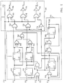
- Fig. 1 of the drawings there is illustrated primarily in block form an array built in self test (ABIST) system of the present invention which shows the main functional elements of the system formed on a semiconductor chip 10, which may be made of silicon.
- the chip 10 includes a memory array 12 having a plurality of horizontally arranged word lines W0, W1, W2, W3, W4, W5 and Wm and a plurality of vertically arranged bit lines B0, B1, B2, B3 and Bn, and a horizontally arranged redundant word line R disposed adjacent to the word line W0.
- the number of word lines may be equal to 256, thus m being equal to 255, and the number of bit lines may be equal to 128, thus n being equal to 127.
- Each of the word lines W0 to Wm and the bit lines B0 to Bn includes a plurality of memory cells located at the intersections of the word lines W0 to Wm and B0 to Bn, identified in Fig. 1 by dots 14. As will be explained hereinbelow, these cells are tested by the ABIST system of the present invention and unacceptable or failed cells are identified as to address locations in the array and replaced by a redundant line. An unacceptable or failed cell is identified in the array 12 of Fig. 1 by an X, with the remaining cells 14 being useful or good cells.
- a good memory cell is a cell which is capable of carrying out its intended data storage function without error, while a faulty memory cell does not function as intended, causing data error.
- the word lines W0 to Wm, the bit lines B0 to Bn and the redundant line R include known driver and sense amplifier circuits for writing information into and reading information out of the cells 14, and that the array 12 may be either a a static random access memory (SRAM) or a dynamic random access memory (DRAM).
- SRAM static random access memory
- DRAM dynamic random access memory
- self test circuits interface with the array 12 through a multiplexer or MUX 16, which generally includes a receiver, under the control of a signal from a test/no-test terminal, multiplexing between address, control and data inputs 18 and test inputs 20, 22 and 24, with signals provided to the address, control and data inputs 18 generally being provided from sources off the chip 10, or from prior logic circuits on chip.
- a test or system control circuit 26 is provided to control a data pattern generator 28 and an address counter 30 which generate the test data and address data, respectively, for the self testing of the memory array 12 through the multiplexer 16.
- test data is written into the memory cells 14 of the array 12 located on the chip 10 and then read out to a data compression unit 32, as is known, where it is compared with the test data written into the cells 14 from the data pattern generator 28. As is also known, the results of the comparison are reduced to a single pass/fail, fault/no fault or master fail signal. These results are applied to a failed address register 34 which may include one or more latches, preferably of the shift register (SRL) type, and which also receives word addresses of the cells 14 of the array 12.
- SRL shift register
- the system control circuit 26 provides per address read/write commands to the array 12, controls address stepping, influences data pattern generation to the array 12 and to the data compression circuit 32 and controls result logging in the failed address register 34.
- expected data from the data pattern generator 28 is applied to the data compression circuit 32 for data output evaluation. This exercise continues until a maximum address flag is issued by the address counter 30 to the system control circuit 26 for providing a new test sequence.
- Three operational phases are pipelined in the ABIST system to sufficiently test any address cell in the array 12. During a first phase, array input data is being set up for the next phase which includes applying the data and address signals to the inputs 20, 22 and 24 of the multiplexer 16.
- the actual data is read out of the array 12, compared in the data compression circuit 32 and the pass/fail or master fail signal provided to the fail address register 34.
- the pass/fail or master fail signal is used to log in or store a word address of a failed cell of the array 12, such as the address of the failed cell of the array 12 indicated at the intersection of word line W1 and the bit line B1, in the fail address register 34.
- an electrical fuse blow interface circuit 36 is activated in response to binary address signals from the failed address register 34 and a fuse blow enabling signal from a terminal FB.
- the terminal FB is a pad or pin on the chip 10 to which the enabling signal is applied from an off chip source after all tests of the array are completed.
- Redundancy fuse circuits 38 including a plurality of fuses, coupled to the outputs of the electrical fuse blow interface circuits 36, are selectively blown depending upon the binary address signals stored in the failed address register 34.
- Outputs from the redundancy fuse circuits 38 are coupled to a suitable address decoder 40 of any known type so as to switch the input address of the defective word line to the redundant word line R. Accordingly, it can be seen that by using only one pad or pin FB on the chip 10, the memory array can be tested and a redundant word line can be substituted for a defective word line even after the chip 10 has been encapsulated or packaged in module form. Thus, it should be noted that modules that fail after burn-in, which is a significant number, can be repaired and fully used by the practice of the present invention.
- Fig. 2 is a circuit diagram in accordance with the teachings of this invention which illustrates in more detail the fail address register 34 and the electrical fuse blow interface circuit 36 shown in Fig. 1 of the drawings.
- the fail address register 34 of Fig. 2 indicated within dashed lines, includes a first latch 42 having a true output T and a data input D connected to an address terminal R0, and a second latch 44 having a clock input cl, a true output T and a data input D connected to an address terminal R1.
- a first AND circuit 46 has a first input connected to a clock terminal CL, which provides clock pulses for the shift register latches (SRL) used in the system of the present invention, and a second input connected to a load result terminal LR, which has a high voltage applied thereto during the testing operation in response to the signals applied to the test/no test terminal indicated in Fig. 1 of the drawings.
- Clock inputs cl in latches 42 and 44 are connected directly to the clock terminal CL.
- a second AND circuit 48 has a first input connected to an output of the first AND circuit 46.
- a third latch 50 has a clock input cl connected to an output of the second AND circuit 48, a data input D connected to the true output T of the first latch 42 and a true output T
- a fourth latch 52 has a clock input cl connected to the output of the second AND circuit 48, a data input connected to the true output T of the second latch 44 and a true output T.
- a first EXCLUSIVE-OR circuit 54 has a first input connected to the true output T of the third latch 50 and a second input connected to the true output T of the first latch 42
- a second EXCLUSIVE-OR circuit 56 has a first input connected to the true output T of the fourth latch 52 and a second input connected to the true output T of the second latch 44.
- a first OR circuit 58 has a first input connected to an output of the second EXCLUSIVE-OR circuit 56 and a second input connected to an output of the first EXCLUSIVE-OR circuit 54.
- a second OR circuit 60 has a first input connected to a pass/fail or master fail terminal FA which is coupled to the output of the data compression circuit 32 shown in Fig. 1 of the drawings.
- a fifth latch 62 has a data input D connected to an output of the second OR circuit 60, a clock input cl connected to the output of the first AND circuit 46, a true output T connected to a second input of the second OR circuit 60 and a complement output C connected to a second input of the second AND circuit 48.
- a third AND circuit 64 has a first input connected to an output of the first OR circuit 58, a second input connected to the true output T of the fifth latch 62 and a third input connected to the master fail terminal FA.
- a third OR circuit 66 has first input connected to an output of the third AND circuit 64, and a sixth latch 68 has a data input D connected to an output of the third OR circuit 66, a clock input cl connected to the output of the first AND circuit 46 and a true output T connected to a second input of the third OR circuit 66 and to an overflow terminal DF.
- the electrical fuse blow interface circuit 36 shown in Fig. 1 of the drawings is illustrated in more detail within the dashed lines 36 in Fig. 2.
- the electrical fuse blow interface circuit 36 includes a first NAND circuit 70 having a first input connected to the true output T of the third latch 50 and a second input connected to the true output of the fifth latch 62, and a second NAND circuit 72 having a first input connected to the true output T of the fourth latch 52 and a second input connected to the true output of the fifth latch 62.
- a first inverter 74 also has an input connected to the true output T of the fifth latch 62.
- a fourth OR circuit 76 has a first input connected to the fuse blow enable signal terminal FB, also shown in Fig.
- a fifth OR circuit 78 has a first input connected to the fuse blow enable signal terminal FB and a second input connected to an output of the first NAND circuit 70 and a sixth OR circuit 80 has a first input connected to the fuse blow enable signal terminal FB and a second input connected to the output of the second NAND circuit 72.
- the electrical fuse blow interface circuit 36 also includes a second inverter 82 having an input connected to an output of the fourth OR circuit 76, a third inverter 84 having an input connected to an output of the fifth OR circuit 78 and a fourth inverter 86 having an input connected to an output of the sixth OR circuit 80.
- a second inverter 82 having an input connected to an output of the fourth OR circuit 76
- a third inverter 84 having an input connected to an output of the fifth OR circuit 78
- a fourth inverter 86 having an input connected to an output of the sixth OR circuit 80.
- the combination of the OR circuits 76, 78 and 80 and the inverters 82, 84 and 86 may be simplified by forming NOR circuits.
- the respective PRGM, PRG0, PRG1 outputs of the inverters 82, 84, 86 are used in conjunction with the FB signal to program the fuse elements.
- the invention utilizes electrically "blowable” fuses.
- any electrically blowable element could be used.
- the element should "blow” by application of a voltage of four volts and a current on the order of 1 mA. This is because substantially higher voltages on-chip will induce dielectric breakdown, latchup, and other deleterious FET failure mechanisms.
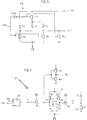
- the programmable fuse element FE utilized in the present invention is shown in Fig. 3 and comprises a polysilicion line F1 having three discrete parts F1a, F1b and F1c coupled to a supply voltage source V dd , and output terminal T and a fuse blow voltage source FB by a plurality of switching transistors Q Fa , Q Fc receives a control signal PRGI at their respective gate electrodes, and transistors Q Fb and Q Fd receive the inverse of PRGI through inverter I FE .
- each of the resistors F1a through F1c is formed from an unsilicided polysilicon conductor strip and have equal resistances.
- each of the resistors has an individual resistance of about 670 ohms.
- the dopant of the unsilicided polysilicon conductor is phosphorous, boron or arsenic.
- transistors Q Fa , Q Fb and Q Fc are off while transistor Q Fd is on. It will be appreciated that in this first condition, resistors F1a, F1b and F1c are connected in series between V dd and terminal T. Q Fd advantageously is turned on to limit current through resistors F1a - F1c to less than the threshold current needed to "blow" the resistors. It will be apparent that, when resistors F1a - F1c provide sufficient series resistance to significantly limit the current through the series connected resistors, the transistor Q Fd can be omitted, allowing transistors Q Fc to control current during both sensing and programming.
- control signals are applied to turn on transistors Q Fa - A Fc , thus coupling resistors F1a - F1c in parallel and producing a current greater than the threshold current in each of the resistors F1a - F1c.
- the resistance of a polysilicon conductor having Na, Nd dopant concentrations greater than 1020/cm3, when subject to a current density J of at least 1.0 x 10⁶ A/cm2 over a period of about 0.5 ⁇ sec, will exhibit a resistance decrease up to about 50 percent due to dopant redistribution.
- the resistance change is non-volatile and non-destructive unless the conductor is again subjected to a current density greater than J or a period of time longer than 0.5 ⁇ sec.
- a threshold current I TH of 1.05 mA would provide the required value of J.
- the threshold current I TH would be at least 5.0 mA, thus requiring an applied voltage of at least 10 V. It will be appreciated that the required voltage is too high to be applied to the entire chip.
- Resistors F1a - F1c when coupled in parallel by transistors Q Fa - Q Fc , permit the required current density to be achieved with a significantly lower applied voltage. In the example where 10 V is applied to produce the required threshold current I TH , an equivalent current density advantageously can be achieved in parallel resistors F1a - F1c with an applied voltage of about 4 V, instead of the previously required 10 V.
- the programmable fuse element FE of Fig. 3 is used as part of a programmable fuse circuit FC shown in Fig. 4 which comprises a plurality of transistors Q L1 through Q L4 operatively connected to form a sensing latch 2 having nodes N1 and N2, and elements FE and F2 operatively coupled to nodes N1 and N2, respectively, via corresponding ones of transistors Q P1 and Q P2 .
- F2 can be a single polysilicon element having the equivalent series resistance equivalent to the three portions F1a, F1b, F1c of F1 prior to fuse blow.
- Sensing latch 2 advantageously amplifies the voltage difference between nodes T and N upon activation of the pass transistors QP1 and QP2 as well as the pulldown of the set node by FB.
- the final state of sensing latch 2 is indicative of the fuse element having the higher resistance.
- One of the nodes N1 and N2 is connected to an output terminal F out via an inverter formed from a pair of transistors Q b1 and Q b2 , which buffer the sensing latch 2 output.
- a signal at F out is equal to voltage V dd when the resistance of F1 is greater than the resistance of F2, while the signal at F out is equal to ground potential GND when the resistance values of F1 and F2 are reversed.
- the redundancy fuse circuits FC indicated in Fig. 4 of the drawings are utilized as the programmable elements FCM, FC0, FC1 as illustrated in Fig. 5 within the dashed lines 38.
- FCM programmable elements
- FC0 programmable elements
- FC1 programmable elements
- FB When FB is lowered, any one of the fuse circuits that have their respective PGR signal high will be programmed, as previously described with reference to FIGS. 3-5.
- the address decoder 40 may be of a known type. However, in order to more clearly disclose the present invention a portion of the circuit diagram of the address decoder 40 is illustrated in Fig. 5 within the dashed lines 40.
- the decoder 40 includes an inverter 120 having an input connected to the output Fout0 of FC0, and an inverter 122 having an input connected to the output Fout1 of FC1.
- a NOR circuit 124 has a first input connected to the output FoutM of FCM and a second input connected to an output Fout0 of FC0.
- a first passgate 126, a second passgate 128, a third passgate 130 and a fourth passgate 132 each include an N-channel field effect transistor connected in parallel with a P-channel field effect transistor.
- the first passgate 126 includes an N-channel transistor 134 and a P-channel transistor 136 connected at a first end to an address terminal W0C
- the second passgate 128 includes an N-channel transistor 138 and a P-channel transistor 140 connected at a first end to an address terminal W0T
- the third passgate 130 includes an N-channel transistor 142 and a P-channel transistor 144 connected at a first end to an address terminal W1C
- the fourth passgate 132 includes an N-channel transistor 146 and a P-channel transistor 148 connected to an address terminal W1T.
- a control electrode of the N-channel transistor 134 is connected to an output of the inverter 120, a control electrode of the P-channel transistor 136 is connected to the Fout0 output, the control electrode of the N-channel transistor 138 is coupled to an output of the NOR circuit 124 through a inverter 150, the control electrode of the P-channel transistor 140 is connected directly to the output of the NOR circuit 124, the control electrode of the N-channel transistor 142 and the control electrode of the P-channel transistor 148 are connected to an output of the tenth inverter 122 and the control electrode of the P-channel transistor 144 and the control electrode of the N-channel transistor 146 are connected to the Fout1 output.
- Transistors 152, 154 and 156 are connected in parallel between a common output terminal F and ground, with a control electrode of the transistor 152 being connected to a second end of the passgate 126, a control electrode of the transistor 154 being connected to a second end of the passgate 128 and a control electrode of the transistor 156 being connected to a second end of each of the passgates 130 and 132.
- a transistor 158 is connected between the control electrode of the transistor 152 and ground with a control electrode connected to the Fout0 output, and a transistor 160 is connected between the control electrode of the transistor 154 and ground with a control electrode connected to the output of the NOR circuit 124.
- Transistors 162 and 164 are connected in parallel between the voltage supply source VH and the common output terminal F, with a control electrode of the transistor 162 being connected to a reset terminal RS and a control electrode of the transistor 164 being connected to ground.
- Each of the transistors 152 through 160 is an N-channel field effect transistor, with the transistors 162 and 164 being P-channel field effect transistors.
- Fig. 1 In the operation of the ABIST system of the present invention it can be seen from Fig. 1 that during test the addresses and particularly the word addresses are applied to the failed address register 34 with the data compression circuit 32 applying a pass/fail or master fail signal to the failed address register 34.
- Fig. 2 of the drawings wherein the word addresses are applied to the terminals R0 and R1 and the pass/fail or master fail signal is applied to the terminal FA.
- the word addresses from the terminals R0 and R1 are applied to the data input D of the latches 42 and 44, respectively, which effectively form a first register, and then are applied from the true output T of the latches 42 and 44 to the data input terminal D of the latches 50 and 52, which form a second register. If a given address is not identified by the master fail signal, e.g., a binary 1 representing a fail and a binary 0 a pass, at the terminal FA as having a failed cell, the address is clocked through the latches 50 and 52, which are preferably of the shift register (SRL) type, from the true outputs T to the first inputs of the EXCLUSIVE-OR circuits 54 and 56.
- SRL shift register
- a subsequent word address which is located in the latches 42 and 44 is simultaneously applied to the second inputs of the EXCLUSIVE-OR circuits 54 and 56. It can be seen that if any of the binary digits of the two addresses differ, a binary 1 or a high voltage of, e.g., 3.6 volts will appear at the output of at least one of the EXCLUSIVE-OR circuits.
- the binary 1 signal is then passed through the OR circuit 58 and applied to the AND circuit 64. However, if there is no indication at the master fail terminal FA that the word line of this word address has a faulty cell, the binary 1 signal does not pass through the AND circuit 64 which also has an input connected to the master terminal FA.
- a binary 1 or high voltage appears simultaneously at the terminal FA.
- This high voltage passes through the OR circuit 60 to the data input D of the latch 62. Since the latches, including latch 62 are initially set, by, e.g., a known Level-Sensitive Scan Design (LSSD) technique, so that the true outputs are low and the complement outputs are high, the high voltage applied to the data input D of the latch 62 causes the true output to go high and the complement output to go low.
- LSSD Level-Sensitive Scan Design
- a low voltage e.g., 0 volts
- the fuse blow enable signal terminal FB which is applied to the electrical fuse blow interface circuit 36, as seen in some detail in Fig. 2 of the drawings.
- the high voltage at the true output T of the latch 62 is applied to each of the second inputs of the NAND circuits 70 and 72 of the electrical fuse blow interface circuit 36 and that the first input of the NAND circuits 70 and 72 are connected to the true output T of the latches 50 and 52, respectively, in which the address of the faulty word line W1 is stored.
- a binary 0 of the word address stored in the latches produces a high voltage at the output of the NAND circuit 72.
- a binary 1 or high voltage at the true output of one of the latches e.g., latch 50, provides a low voltage at the output of the NAND circuit 70 resulting in a high voltage at the PGR0 output.
- the electrical fuse blow interface circuit 36 also has a high voltage applied to the input of the inverter 74 from the true output T of the latch 62 providing a low voltage at the second input of the OR circuit 76, along with the low voltage provided to the first input of the OR circuit 76 from the fuse blow enabling signal terminal FB, resulting in a high voltage at the PGRM output.
- Fig. 3 of the drawings it can be seen that with the PGR1 input at 1 and FB low, all three elements F1a, F1b, F1c are connected directly to the voltage supply source Vdd or VH and designed to blow with the full supply voltage applied across it, the fuse elements blow to set output T at a high voltage.
- the Fout0 and FoutM outputs will be permanently maintained at 0 volts.
- the fuse elements F1a, F1b, F1c will not change, such that node N1 will set low and Fout1 will be permanently set at a high voltage.
- the passgate 130 of the address decoder 40 With Fout1 at a high voltage, the passgate 130 of the address decoder 40 is turned on, whereas the passgate 132 is turned off.
- Applied to the terminals W1T and W1C are true and complement address signals produced by a receiver disposed in the MUX 16 and fed to the address decoder 40 through address lines in a well known manner. If the true address is high and the complement is low the transistor 156 will not turn on. With the terminal U0 at a low voltage, the passgate 126 is turned off. With the terminal UM low, along with a low voltage at the terminal U0, passgate 128 is turned on.
- the terminal F is discharged to ground indicating that the array 12 does not need redundancy substitution for this address.
- the fuse links in the circuits of the present invention are either open or closed, thus effectively storing binary digits of 1 or 0.
- redundant word line Although only one redundant word line was illustrated in the figures of the drawings, it should be understood that two or more redundant lines may be use in accordance with the teachings of this invention by providing additional registers for storing the faulty addresses along with appropriate additional latches to hold the faulty addresses in these additional registers. Furthermore, two or more memory arrays or subarrays each having one or more redundant lines on a single chip may utilize the teachings of this invention by providing a sufficient number of registers and holding latches along with appropriate array selection logic circuits.
- the fail address register 34 in Fig. 2 Illustrated in the drawings, in, e.g., the fail address register 34 in Fig. 2, are only two terminals R0 and R1 for receiving the binary bits of the word line addresses. It should be understood, however, that additional address terminals, e.g., a total of eight, depending on the number of word lines used in the array, indicated by a series of dots, may be provided with corresponding latches and logic circuits coupled thereto. In a typical currently used memory array, 256 word lines and 128 bit lines are used which would require word addresses with eight binary digits applied in parallel to eight address terminals in the fail address register 34.
- an ABIST system is used to identify and store faulty array lines and then to substitute a redundant line for the identified faulty array line by merely toggling the voltage at one pad or pin on the semiconductor chip carrying the memory array. Since the substitution of the redundant line for the faulty array line requires only a change in voltage at one pad or pin of the chip, array testing and redundancy may be carried out after burn-in or even in the field after the chip has been packaged in module form. Since burn-in often uncovers a weak or faulty cell in an array, the use of this invention, employing an electronic redundancy technique, can dramatically increase the yield of a high performance product having a memory array embedded therein. In some products it has been found that 50 to 60% of the burn-in fails could be repaired by using the teachings of the present invention.
Abstract
A redundancy system formed on a semiconductor chip is provided which includes circuits for testing a memory array to locate a faulty element therein, a register for storing an address of the faulty element and electrical fuses blown in response to binary digits of the address stored in the register upon application of an enable signal from a single input to the semiconductor chip. The enable signal passes through logic circuits on the chip such that the fuses cannot be programmed or blown unless the enable signal is present. An address decoder coupled to outputs from the fuses substitutes a redundant element for the faulty element.
Description
- This invention relates to an array built in self test (ABIST) system which provides for memory testing and replacement of failed elements in an array after module assembly.
- Replacement of failed elements or lines in a memory array formed on a chip or substrate by the use of redundant elements or lines provided on the chip or substrate has been known. Redundancy techniques have generally used laser beams to blow fuses formed on a substrate at wafer levels. In this manner redundant elements are used to replace failing elements. Thereafter the wafer is diced into chips and the chips are mounted in a module. After completion of the module burn-in takes place. Any elements that fail burn-in are discarded or undergo disassembly of the module and expensive repairs.
- A chip that integrates various kinds of circuits including logic circuits having memory arrays embedded therein poses special problems for circuit designers/testers who desire adequate testability of the embedded arrays since such chips have fewer input/output pins available to the circuit testers than is available in a chip having a stand alone memory.
- To lower the cost of making memories by reducing testing expenses and improving memory yields, systems have been disclosed which are self testing and self repairing. One such system, sometimes known as an array built in self test (ABIST) system, is taught in U.S. Patent No. 4,939,694, issued on July 30, 1990, which uses substitute address tables and error correction code (ECC) techniques for correcting errors found in the memory cell. Another ABIST system, disclosed in European Patent No. 0 242 854, published on October 28, 1987, replaces defective memory cells of a semiconductor memory with spare memory cells using an associative memory. U.S. Patent No. 3,755,791, issued on August 28, 1973, filed by L. M. Arzubi, and IBM Technical Disclosure Bulletin, Vol. 23, No. 8, pp. 3601 and 3602, entitled "Semiconductor Memory Redundancy at Module Level" by B. F. Fitzgerald and D. R. Whittaker, disclose the use of non-volatile cells for storing failing addresses semi-permanently. A further ABIST system is disclosed in U.S. patent application entitled "Built-In Self Test for Integrated Circuits" and having Serial No. 07/576646, filed on August 30, 1990, by E. L. Hedberg et al., wherein one dimensional failed address registers are used to store word addresses of defective cells of a memory array, i.e., redundant lines are provided which extend in only one direction parallel to the word lines of the array. U.S. patent application entitled "Method and Apparatus for Real Time Two Dimensional Redundancy Allocation" filed on October 16, 1991, by E. L. Hedberg and G. S. Koch, having Serial No. 07/777,877, discloses an ABIST system wherein two dimensional redundant lines are directly allocated in real time during final manufacturing testing to increase semiconductor chip yields. U.S. patent application entitled "Low Voltage Programmable Storage Element", filed on April 30, 1991, having Serial No. 07/693,463, discloses programmable redundancy wherein resistance decreases in a programmable antifuse circuit are sensed.
- It is an object of this invention is to provide an improved array built in self testing system on a semiconductor chip wherein testing and replacement of faulty elements in an array occurs after the chip on which the array has been formed has been packaged in a module.
- In accordance with the teachings of this invention, an improved array built in self test system is provided on a semiconductor chip which includes means for storing an address of a faulty element of an array, an electrical fuse having a first end thereof coupled to a first terminal of a supply voltage and means responsive to an enabling signal and to the address stored in the storing means for selectively coupling a second end of the fuse to a second terminal of the supply voltage to switch input signals representative of the address of the faulty element to signals representative of a redundant line.
- The foregoing and other objects, features and advantages of the invention will be apparent from the following more particular description of the preferred embodiments of the invention, as illustrated in the accompanying drawings.
-
- Fig. 1
- is primarily a block diagram of an array built in test (ABIST) system of the present invention,
- Fig. 2
- is a circuit diagram illustrating in more detail failed address register and electrical fuse blow circuits indicated in the ABIST system shown in Fig. 1 of the drawings,
- Fig. 3
- is a circuit diagram of a fuse element FE of the invention,
- Fig. 4
- is a circuit diagram of the fuse circuit FC of the invention, which utilizes element FE of Fig. 3, and
- Fig. 5
- is a circuit diagram illustrating in more detail redundancy fuse circuits and some of the circuits of the address decoder indicated in the ABIST system shown in Fig. 1 of the drawings.
- Referring to Fig. 1 of the drawings in more detail, there is illustrated primarily in block form an array built in self test (ABIST) system of the present invention which shows the main functional elements of the system formed on a
semiconductor chip 10, which may be made of silicon. Thechip 10 includes amemory array 12 having a plurality of horizontally arranged word lines W0, W1, W2, W3, W4, W5 and Wm and a plurality of vertically arranged bit lines B0, B1, B2, B3 and Bn, and a horizontally arranged redundant word line R disposed adjacent to the word line W0. If desired, the number of word lines may be equal to 256, thus m being equal to 255, and the number of bit lines may be equal to 128, thus n being equal to 127. Also, more than one redundant line may be provided on thechip 10. Each of the word lines W0 to Wm and the bit lines B0 to Bn includes a plurality of memory cells located at the intersections of the word lines W0 to Wm and B0 to Bn, identified in Fig. 1 bydots 14. As will be explained hereinbelow, these cells are tested by the ABIST system of the present invention and unacceptable or failed cells are identified as to address locations in the array and replaced by a redundant line. An unacceptable or failed cell is identified in thearray 12 of Fig. 1 by an X, with theremaining cells 14 being useful or good cells. A good memory cell is a cell which is capable of carrying out its intended data storage function without error, while a faulty memory cell does not function as intended, causing data error. It should be understood that the word lines W0 to Wm, the bit lines B0 to Bn and the redundant line R include known driver and sense amplifier circuits for writing information into and reading information out of thecells 14, and that thearray 12 may be either a a static random access memory (SRAM) or a dynamic random access memory (DRAM). - As indicated in Fig. 1 of the drawings, self test circuits interface with the
array 12 through a multiplexer orMUX 16, which generally includes a receiver, under the control of a signal from a test/no-test terminal, multiplexing between address, control anddata inputs 18 andtest inputs data inputs 18 generally being provided from sources off thechip 10, or from prior logic circuits on chip. A test orsystem control circuit 26 is provided to control adata pattern generator 28 and anaddress counter 30 which generate the test data and address data, respectively, for the self testing of thememory array 12 through themultiplexer 16. The test data is written into thememory cells 14 of thearray 12 located on thechip 10 and then read out to adata compression unit 32, as is known, where it is compared with the test data written into thecells 14 from thedata pattern generator 28. As is also known, the results of the comparison are reduced to a single pass/fail, fault/no fault or master fail signal. These results are applied to a failedaddress register 34 which may include one or more latches, preferably of the shift register (SRL) type, and which also receives word addresses of thecells 14 of thearray 12. - The
system control circuit 26 provides per address read/write commands to thearray 12, controls address stepping, influences data pattern generation to thearray 12 and to thedata compression circuit 32 and controls result logging in the failedaddress register 34. During a read operation, expected data from thedata pattern generator 28 is applied to thedata compression circuit 32 for data output evaluation. This exercise continues until a maximum address flag is issued by theaddress counter 30 to thesystem control circuit 26 for providing a new test sequence. Three operational phases are pipelined in the ABIST system to sufficiently test any address cell in thearray 12. During a first phase, array input data is being set up for the next phase which includes applying the data and address signals to theinputs multiplexer 16. Then during the next phase, the actual data is read out of thearray 12, compared in thedata compression circuit 32 and the pass/fail or master fail signal provided to thefail address register 34. During the last phase, the pass/fail or master fail signal is used to log in or store a word address of a failed cell of thearray 12, such as the address of the failed cell of thearray 12 indicated at the intersection of word line W1 and the bit line B1, in thefail address register 34. - After the array has been fully tested and a word address has been stored in the failed
address register 34, indicating the presence of a faulty cell in thearray 12, an electrical fuseblow interface circuit 36 is activated in response to binary address signals from the failedaddress register 34 and a fuse blow enabling signal from a terminal FB. The terminal FB is a pad or pin on thechip 10 to which the enabling signal is applied from an off chip source after all tests of the array are completed.Redundancy fuse circuits 38 including a plurality of fuses, coupled to the outputs of the electrical fuseblow interface circuits 36, are selectively blown depending upon the binary address signals stored in the failedaddress register 34. Outputs from theredundancy fuse circuits 38 are coupled to asuitable address decoder 40 of any known type so as to switch the input address of the defective word line to the redundant word line R. Accordingly, it can be seen that by using only one pad or pin FB on thechip 10, the memory array can be tested and a redundant word line can be substituted for a defective word line even after thechip 10 has been encapsulated or packaged in module form. Thus, it should be noted that modules that fail after burn-in, which is a significant number, can be repaired and fully used by the practice of the present invention. - Fig. 2 is a circuit diagram in accordance with the teachings of this invention which illustrates in more detail the
fail address register 34 and the electrical fuseblow interface circuit 36 shown in Fig. 1 of the drawings. The fail address register 34 of Fig. 2, indicated within dashed lines, includes afirst latch 42 having a true output T and a data input D connected to an address terminal R0, and asecond latch 44 having a clock input cl, a true output T and a data input D connected to an address terminal R1. A first ANDcircuit 46 has a first input connected to a clock terminal CL, which provides clock pulses for the shift register latches (SRL) used in the system of the present invention, and a second input connected to a load result terminal LR, which has a high voltage applied thereto during the testing operation in response to the signals applied to the test/no test terminal indicated in Fig. 1 of the drawings. Clock inputs cl inlatches circuit 48 has a first input connected to an output of the first ANDcircuit 46. Athird latch 50 has a clock input cl connected to an output of the second ANDcircuit 48, a data input D connected to the true output T of thefirst latch 42 and a true output T, and afourth latch 52 has a clock input cl connected to the output of the second ANDcircuit 48, a data input connected to the true output T of thesecond latch 44 and a true output T. A first EXCLUSIVE-OR circuit 54 has a first input connected to the true output T of thethird latch 50 and a second input connected to the true output T of thefirst latch 42, and a second EXCLUSIVE-OR circuit 56 has a first input connected to the true output T of thefourth latch 52 and a second input connected to the true output T of thesecond latch 44. A first ORcircuit 58 has a first input connected to an output of the second EXCLUSIVE-OR circuit 56 and a second input connected to an output of the first EXCLUSIVE-OR circuit 54. - A second OR
circuit 60 has a first input connected to a pass/fail or master fail terminal FA which is coupled to the output of thedata compression circuit 32 shown in Fig. 1 of the drawings. Afifth latch 62 has a data input D connected to an output of the second ORcircuit 60, a clock input cl connected to the output of the first ANDcircuit 46, a true output T connected to a second input of the second ORcircuit 60 and a complement output C connected to a second input of the second ANDcircuit 48. A third ANDcircuit 64 has a first input connected to an output of the first ORcircuit 58, a second input connected to the true output T of thefifth latch 62 and a third input connected to the master fail terminal FA. A third ORcircuit 66 has first input connected to an output of the third ANDcircuit 64, and asixth latch 68 has a data input D connected to an output of the third ORcircuit 66, a clock input cl connected to the output of the first ANDcircuit 46 and a true output T connected to a second input of the third ORcircuit 66 and to an overflow terminal DF. - The electrical fuse
blow interface circuit 36 shown in Fig. 1 of the drawings is illustrated in more detail within the dashedlines 36 in Fig. 2. The electrical fuseblow interface circuit 36 includes afirst NAND circuit 70 having a first input connected to the true output T of thethird latch 50 and a second input connected to the true output of thefifth latch 62, and asecond NAND circuit 72 having a first input connected to the true output T of thefourth latch 52 and a second input connected to the true output of thefifth latch 62. Afirst inverter 74 also has an input connected to the true output T of thefifth latch 62. A fourth ORcircuit 76 has a first input connected to the fuse blow enable signal terminal FB, also shown in Fig. 1 of the drawings, and a second input connected to an output of thefirst inverter 74, a fifth ORcircuit 78 has a first input connected to the fuse blow enable signal terminal FB and a second input connected to an output of thefirst NAND circuit 70 and a sixth ORcircuit 80 has a first input connected to the fuse blow enable signal terminal FB and a second input connected to the output of thesecond NAND circuit 72. - The electrical fuse
blow interface circuit 36 also includes asecond inverter 82 having an input connected to an output of the fourth ORcircuit 76, athird inverter 84 having an input connected to an output of the fifth ORcircuit 78 and afourth inverter 86 having an input connected to an output of the sixth ORcircuit 80. Of course, as is known, if desired, the combination of theOR circuits inverters inverters - As stated previously, the invention utilizes electrically "blowable" fuses. As a practical matter any electrically blowable element could be used. In the invention, the element should "blow" by application of a voltage of four volts and a current on the order of 1 mA. This is because substantially higher voltages on-chip will induce dielectric breakdown, latchup, and other deleterious FET failure mechanisms. In the invention it is preferred to use an unsolicited, doped polysilicon line as a fuse element. Upon application of a given current density, the poly line exhibits a discrete decrease in resistance. See an article by Kato et al, "A Physical Mechanism of Current-Induced Resistance Decrease in Heavily Doped Polysilicon Resistors," IEEE Transactions on Electron Devices, Vol. ED-29, No. 8, August 1982 pp. 1156-61. This phenomena has been used previously to construct an electrically blowable fuse element. See US Patent Application S.N. 07/693,463 by W. Abadeer et al, entitled "Low Voltage Programmable Storage Element," the teachings of which are incorporated herein by reference. The invention utilizes a modified version of the fuse disclosed in the Abadeer et al. patent application. These modifications will be described in more detail below.
- The programmable fuse element FE utilized in the present invention is shown in Fig. 3 and comprises a polysilicion line F1 having three discrete parts F1a, F1b and F1c coupled to a supply voltage source Vdd, and output terminal T and a fuse blow voltage source FB by a plurality of switching transistors QFa, QFc receives a control signal PRGI at their respective gate electrodes, and transistors QFb and QFd receive the inverse of PRGI through inverter IFE. Preferably, each of the resistors F1a through F1c is formed from an unsilicided polysilicon conductor strip and have equal resistances. For example, when the total series resistance of the programmable antifuse circuit F1 is 2000 ohms, each of the resistors has an individual resistance of about 670 ohms. Preferably, the dopant of the unsilicided polysilicon conductor is phosphorous, boron or arsenic.
- When sensing the programming state of the resistors Fla-Flc, transistors QFa, QFb and QFc are off while transistor QFd is on. It will be appreciated that in this first condition, resistors F1a, F1b and F1c are connected in series between Vdd and terminal T. QFd advantageously is turned on to limit current through resistors F1a - F1c to less than the threshold current needed to "blow" the resistors. It will be apparent that, when resistors F1a - F1c provide sufficient series resistance to significantly limit the current through the series connected resistors, the transistor QFd can be omitted, allowing transistors QFc to control current during both sensing and programming. During programming of antifuse F1, control signals are applied to turn on transistors QFa - AFc, thus coupling resistors F1a - F1c in parallel and producing a current greater than the threshold current in each of the resistors F1a - F1c.
- As disclosed in the Kato et al. reference, discussed above, the resistance of a polysilicon conductor having Na, Nd dopant concentrations greater than 10²⁰/cm³, when subject to a current density J of at least 1.0 x 10⁶ A/cm² over a period of about 0.5 µsec, will exhibit a resistance decrease up to about 50 percent due to dopant redistribution. The resistance change is non-volatile and non-destructive unless the conductor is again subjected to a current density greater than J or a period of time longer than 0.5 µsec. Assuming the polysilicon conductor has cross section dimensions of 0.3 x 10⁻⁴ cm and 0.35 x 10⁻⁴ cm, in an exemplary case, a threshold current ITH of 1.05 mA would provide the required value of J. In another exemplary case, where the series resistance of F1 is 2000 ohms and fuse element cross section is 350 nanometers by 600 nanometers, the threshold current ITH would be at least 5.0 mA, thus requiring an applied voltage of at least 10 V. It will be appreciated that the required voltage is too high to be applied to the entire chip. Resistors F1a - F1c, when coupled in parallel by transistors QFa - QFc, permit the required current density to be achieved with a significantly lower applied voltage. In the example where 10 V is applied to produce the required threshold current ITH, an equivalent current density advantageously can be achieved in parallel resistors F1a - F1c with an applied voltage of about 4 V, instead of the previously required 10 V.
- The programmable fuse element FE of Fig. 3 is used as part of a programmable fuse circuit FC shown in Fig. 4 which comprises a plurality of transistors QL1 through QL4 operatively connected to form a sensing latch 2 having nodes N1 and N2, and elements FE and F2 operatively coupled to nodes N1 and N2, respectively, via corresponding ones of transistors QP1 and QP2. F2 can be a single polysilicon element having the equivalent series resistance equivalent to the three portions F1a, F1b, F1c of F1 prior to fuse blow. Transistor QFd in Fig. 3 draws the same current through F1a-F1c as does device Qs2 through F2, to convert a resistance difference between F1 and F2 into a voltage difference between node T (output of FE) and node N. Sensing latch 2 advantageously amplifies the voltage difference between nodes T and N upon activation of the pass transistors QP1 and QP2 as well as the pulldown of the set node by FB. Preferably, the final state of sensing latch 2 is indicative of the fuse element having the higher resistance. One of the nodes N1 and N2 is connected to an output terminal Fout via an inverter formed from a pair of transistors Qb1 and Qb2, which buffer the sensing latch 2 output. For the programmable storage element FE shown in Fig. 3, a signal at Fout is equal to voltage Vdd when the resistance of F1 is greater than the resistance of F2, while the signal at Fout is equal to ground potential GND when the resistance values of F1 and F2 are reversed.
- The redundancy fuse circuits FC indicated in Fig. 4 of the drawings are utilized as the programmable elements FCM, FC0, FC1 as illustrated in Fig. 5 within the dashed lines 38. When FB is lowered, any one of the fuse circuits that have their respective PGR signal high will be programmed, as previously described with reference to FIGS. 3-5.
- As set forth hereinabove in connection with the description of the block diagram in Fig. 1, the
address decoder 40 may be of a known type. However, in order to more clearly disclose the present invention a portion of the circuit diagram of theaddress decoder 40 is illustrated in Fig. 5 within the dashed lines 40. Thedecoder 40 includes aninverter 120 having an input connected to the output Fout0 of FC0, and aninverter 122 having an input connected to the output Fout1 of FC1. A NORcircuit 124 has a first input connected to the output FoutM of FCM and a second input connected to an output Fout0 of FC0. Afirst passgate 126, asecond passgate 128, athird passgate 130 and afourth passgate 132 each include an N-channel field effect transistor connected in parallel with a P-channel field effect transistor. Thefirst passgate 126 includes an N-channel transistor 134 and a P-channel transistor 136 connected at a first end to an address terminal W0C, thesecond passgate 128 includes an N-channel transistor 138 and a P-channel transistor 140 connected at a first end to an address terminal W0T, thethird passgate 130 includes an N-channel transistor 142 and a P-channel transistor 144 connected at a first end to an address terminal W1C and thefourth passgate 132 includes an N-channel transistor 146 and a P-channel transistor 148 connected to an address terminal W1T. A control electrode of the N-channel transistor 134 is connected to an output of theinverter 120, a control electrode of the P-channel transistor 136 is connected to the Fout0 output, the control electrode of the N-channel transistor 138 is coupled to an output of the NORcircuit 124 through ainverter 150, the control electrode of the P-channel transistor 140 is connected directly to the output of the NORcircuit 124, the control electrode of the N-channel transistor 142 and the control electrode of the P-channel transistor 148 are connected to an output of thetenth inverter 122 and the control electrode of the P-channel transistor 144 and the control electrode of the N-channel transistor 146 are connected to the Fout1 output.Transistors transistor 152 being connected to a second end of thepassgate 126, a control electrode of thetransistor 154 being connected to a second end of thepassgate 128 and a control electrode of thetransistor 156 being connected to a second end of each of thepassgates transistor 158 is connected between the control electrode of thetransistor 152 and ground with a control electrode connected to the Fout0 output, and atransistor 160 is connected between the control electrode of thetransistor 154 and ground with a control electrode connected to the output of the NORcircuit 124.Transistors transistor 162 being connected to a reset terminal RS and a control electrode of thetransistor 164 being connected to ground. Each of thetransistors 152 through 160 is an N-channel field effect transistor, with thetransistors - In the operation of the ABIST system of the present invention it can be seen from Fig. 1 that during test the addresses and particularly the word addresses are applied to the failed address register 34 with the
data compression circuit 32 applying a pass/fail or master fail signal to the failedaddress register 34. This can be seen in more detail by referring to Fig. 2 of the drawings wherein the word addresses are applied to the terminals R0 and R1 and the pass/fail or master fail signal is applied to the terminal FA. The word addresses from the terminals R0 and R1 are applied to the data input D of thelatches latches latches latches OR circuits latches OR circuits OR circuit 58 and applied to the ANDcircuit 64. However, if there is no indication at the master fail terminal FA that the word line of this word address has a faulty cell, the binary 1 signal does not pass through the ANDcircuit 64 which also has an input connected to the master terminal FA. - When the word address of a faulty cell, such as cell W1,B1 in the word line W1 of the
array 12, indicated in Fig. 1 of the drawings, is being applied to thelatches OR circuit 60 to the data input D of thelatch 62. Since the latches, includinglatch 62 are initially set, by, e.g., a known Level-Sensitive Scan Design (LSSD) technique, so that the true outputs are low and the complement outputs are high, the high voltage applied to the data input D of thelatch 62 causes the true output to go high and the complement output to go low. With the complement output C of thelatch 62 being low, clock pulses from the clock terminal CL can no longer pass through the ANDcircuit 48 to thelatches latches - If the word address of a second faulty cell which does not have the same word address as that of the first faulty cell W1,B1 is applied to the data inputs D of the
latches OR circuits circuit 64 through theOR circuit 58. Since the voltage at the true output of thelatch 62 is high and since the voltage at the master fail terminal is now high, a high voltage will appear at the output of the ANDcircuit 64 to cause the true output T of thelatch 68 to go high, indicating at the overflow terminal DF that thearray 12 has too many word lines with faulty cells to be repaired, since in this embodiment of the invention only one redundant word line R has been provided. - If after the testing procedure has been completed and only one faulty word line, W1, has been identified, a low voltage, e.g., 0 volts, is provided at the fuse blow enable signal terminal FB which is applied to the electrical fuse
blow interface circuit 36, as seen in some detail in Fig. 2 of the drawings. It should be noted that the high voltage at the true output T of thelatch 62 is applied to each of the second inputs of theNAND circuits blow interface circuit 36 and that the first input of theNAND circuits latches latch 52, produces a high voltage at the output of theNAND circuit 72. With a high voltage at the output of theNAND circuit 72, a low voltage is provided at the PRG1 output. Likewise it can be seen that a binary 1 or high voltage at the true output of one of the latches, e.g., latch 50, provides a low voltage at the output of theNAND circuit 70 resulting in a high voltage at the PGR0 output. - The electrical fuse
blow interface circuit 36 also has a high voltage applied to the input of theinverter 74 from the true output T of thelatch 62 providing a low voltage at the second input of theOR circuit 76, along with the low voltage provided to the first input of theOR circuit 76 from the fuse blow enabling signal terminal FB, resulting in a high voltage at the PGRM output. - Turning to Fig. 3 of the drawings, it can be seen that with the PGR1 input at 1 and FB low, all three elements F1a, F1b, F1c are connected directly to the voltage supply source Vdd or VH and designed to blow with the full supply voltage applied across it, the fuse elements blow to set output T at a high voltage. This causes the latch 2 of Fig. 4 to set node N1 high (the pass devices QP1, QP2 as well as the set node being activated by FB), causing Fout to go low. Thus, in Fig. 5, with PGR0 and PGRM high, the Fout0 and FoutM outputs will be permanently maintained at 0 volts. For FC1, with PRG1 low the fuse elements F1a, F1b, F1c will not change, such that node N1 will set low and Fout1 will be permanently set at a high voltage.
- With Fout1 at a high voltage, the
passgate 130 of theaddress decoder 40 is turned on, whereas thepassgate 132 is turned off. Applied to the terminals W1T and W1C are true and complement address signals produced by a receiver disposed in theMUX 16 and fed to theaddress decoder 40 through address lines in a well known manner. If the true address is high and the complement is low thetransistor 156 will not turn on. With the terminal U0 at a low voltage, thepassgate 126 is turned off. With the terminal UM low, along with a low voltage at the terminal U0,passgate 128 is turned on. Accordingly, it can be seen that if there is a match between the addresses and the fuses, i.e., if the fuse is not blown and the corresponding true address is high or if the fuse is blown and the corresponding true address is low, none of thetransistors transistor 164 merely acts as a bleeder resistor to prevent discharge of the terminal F until at least one of thetransistors address decoder 40 substitutes the redundant word line R for the defective word line W1 in a known manner. If any one of thetransistors array 12 does not need redundancy substitution for this address. It should be noted that the fuse links in the circuits of the present invention are either open or closed, thus effectively storing binary digits of 1 or 0. - Although only one redundant word line was illustrated in the figures of the drawings, it should be understood that two or more redundant lines may be use in accordance with the teachings of this invention by providing additional registers for storing the faulty addresses along with appropriate additional latches to hold the faulty addresses in these additional registers. Furthermore, two or more memory arrays or subarrays each having one or more redundant lines on a single chip may utilize the teachings of this invention by providing a sufficient number of registers and holding latches along with appropriate array selection logic circuits.
- Illustrated in the drawings, in, e.g., the
fail address register 34 in Fig. 2, are only two terminals R0 and R1 for receiving the binary bits of the word line addresses. It should be understood, however, that additional address terminals, e.g., a total of eight, depending on the number of word lines used in the array, indicated by a series of dots, may be provided with corresponding latches and logic circuits coupled thereto. In a typical currently used memory array, 256 word lines and 128 bit lines are used which would require word addresses with eight binary digits applied in parallel to eight address terminals in thefail address register 34. - Accordingly, it can be seen that in accordance with the teachings of this invention, an ABIST system is used to identify and store faulty array lines and then to substitute a redundant line for the identified faulty array line by merely toggling the voltage at one pad or pin on the semiconductor chip carrying the memory array. Since the substitution of the redundant line for the faulty array line requires only a change in voltage at one pad or pin of the chip, array testing and redundancy may be carried out after burn-in or even in the field after the chip has been packaged in module form. Since burn-in often uncovers a weak or faulty cell in an array, the use of this invention, employing an electronic redundancy technique, can dramatically increase the yield of a high performance product having a memory array embedded therein. In some products it has been found that 50 to 60% of the burn-in fails could be repaired by using the teachings of the present invention.
- While the invention has been particularly shown and described with reference to preferred embodiments thereof, it will be understood by those skilled in the art that various changes in form and details may be made therein without departing from the spirit and scope of the invention.
Claims (23)
- An array built in self test (ABIST) system formed on a semiconductor chip comprising
a memory array including a plurality of word lines, one of which is faulty, and a redundant word line,
means for identifying said faulty word line,
means for storing an address of said faulty word line,
a plurality of fuses,
interface circuit means coupling said address storing to said plurality of fuses,
enabling signal means coupled to said interface circuit means for blowing selected one or more of said plurality of fuses depending upon the address of said faulty word line stored in said storing means, and
switching means coupled to outputs of said interface circuit means for replacing said faulty word line with said redundant word line. - An array built in self test (ABIST) system as set forth in claim 1 wherein said enabling signal means includes a terminal on said semiconductor chip having an enabling signal applied thereto.
- An array built in self test (ABIST) system as set forth in claim 2 wherein said terminal is a pad disposed on said semiconductor chip.
- An array built in self test (ABIST) system as set forth in claim 3 wherein said enabling signal means further includes a master fail signal derived from said identifying means.
- An array built in self test (ABIST) system as set forth in claim 1 wherein each of the fuses of said plurality of fuses is made of doped polysilicon.
- An array built in self test (ABIST) system as set forth in claim 4 further including a voltage supply source connected to a first end of each of the fuses of said plurality of fuses, and a second end of said plurality of fuses being connected to outputs of said interface circuit means.
- An array built in self test (ABIST) system as set forth in claim 6 wherein a second end of one of said plurality of fuses is coupled to said identifying means.
- An array built in self test (ABIST) system as set forth in claim 1 wherein said switching means includes an address decoder.
- An array built in self test (ABIST) system formed on a semiconductor chip and having a power supply source of a given voltage comprising
a memory array including a plurality of word lines, one of which is faulty, and a redundant word line,
means for identifying said faulty word line,
means for storing a multi-bit address of said faulty word line,
a plurality of fuses, each being selectively coupled to said power supply source,
interface circuit means coupling respective ones of the bits of said multi-bit address to respective ones of said plurality of fuses,
enabling signal means coupled to said interface circuit means for connecting selected ones of said plurality of fuses to said power supply source depending upon the address of said faulty word line stored in said address storing means, and
switching means coupled to outputs of said interface circuit means for replacing said faulty word line with said redundant word line. - An array built in self test (ABIST) system as set forth in claim 9 wherein said enabling signal means includes a terminal on said semiconductor chip having an enabling signal applied thereto.
- An array built in self test (ABIST) system as set forth in claim 10 wherein said terminal is a pin disposed on said semiconductor chip.
- An array built in self test (ABIST) system as set forth in claim 11 wherein said enabling signal means further includes a master fail signal derived from said identifying means.
- An array built in self test (ABIST) system as set forth in claim 12 wherein said switching means includes an address decoder.
- An array built in self test (ABIST) system formed on a semiconductor chip having a pad disposed thereon comprising
a memory array including a plurality of word lines, one of which is a faulty word line, and a redundant word line,
data compression means for providing a signal to identify said faulty word line,
failed address register means responsive to said signal for storing an address of said faulty word line,
electrical fuse blow interface means responsive to said signal applied to said pad,
redundancy fuse circuit means including a plurality of fuses coupled to outputs of said electrical fuse blow interface means for blowing selected fuses of said plurality of fuses depending upon the address of said faulty word line, and
address decoder means coupled to said redundancy fuse circuit means for substituting said redundant word line for said faulty word line. - An array built in self test (ABIST) system as set forth in claim 14 wherein each of said fuses is made of doped polysilicon.
- A system formed on a semiconductor chip comprising
an electrical terminal disposed on said chip having a fuse blow enabling signal applied thereto,
a memory array including a plurality of word lines having a faulty word line and a redundant word line,
means for providing a control signal to identify said faulty word line,
means responsive to said control signal for storing an address of said faulty word line,
a plurality of fuses,
interface circuit means responsive to said control signal and to said fuse blow enable signal coupling said address storing means to said plurality of fuses for blowing selected one or more of said plurality of fuses depending upon the address of said faulty word line, and
switching means coupled to outputs of said interface circuit means for replacing said faulty word line with said redundant word line. - A system as set forth in claim 16 wherein said terminal is a conductive pad.
- A system as set forth in claim 16 wherein said means for storing includes a register and said switching means includes an address decoder.
- In a memory device mounted on a substrate including a plurality of lines of first memory cells, each line having a discrete x-bit address, a fault detection and recovery apparatus comprising
at least one line of second spare memory cells,
first means for temporarily storing an x-bit address of at least one of said plurality of lines of first memory cells determined to be faulty,
fuse means for permanently storing said x-bit address of said at least one of said plurality of lines of first memory cells so that said at least one line of second spare memory cells is substituted for said at least one of said plurality of first memory cells, and
third means responding to an enable signal for programming said fuse means to permanently store said x-bit address from said first means, said third means preventing said fuse means from being programmed in the absence of said enable signal. - In a memory device mounted on a substrate as set forth in claim 19 wherein said fuse means includes a plurality of fuses each having a first end connected to a voltage supply source and said third means is coupled to a second end to a second end of the fuses of said plurality of fuses.
- An array built in self test (ABIST) system formed on a semiconductor chip packaged within a module comprising
an array having a faulty element therein and a redundant element,
means for storing an address signal of said faulty element,
an electrical fuse having a first end thereof connected to a first terminal of a voltage supply source,
a terminal disposed on said semiconductor chip having an enabling signal applied thereto, and
means responsive to said enabling signal and to the address signal for selectively coupling a second end of said electrical fuse to a second terminal of said voltage supply source to switch signals representative of the address of said faulty element to said redundant element. - An array built in self test (ABIST) system as set forth in claim 10
wherein said identifying means includes an output having a master fail signal thereon and
wherein said interface circuit means includes at least one NAND circuit having first and second inputs and an output and an OR circuit having first and second inputs and an output, the first input of said NAND circuit being connected to said storing means, the second input of said NAND circuit being coupled to the output of said identifying means, the first input of said OR circuit being connected to the terminal of said enabling signal means, the second input of said OR circuit being connected to the output of said NAND circuit and the output of said OR circuit being coupled to the second end of said plurality of fuses. - An array built in self address (ABIST) system as set forth in claim 22 wherein said interface circuit means further includes an inverter having an input and an output disposed between the output of said OR circuit and the second end of said plurality of fuses and an N-channel field effect transistor having a control electrode connected between the terminal of said enabling signal means and the second end of said plurality of fuses, the input of said inverter being connected to the output of said OR circuit and the output of said inverter being connected to the control electrode of said transistor.
Applications Claiming Priority (2)
| Application Number | Priority Date | Filing Date | Title |
|---|---|---|---|
| US852587 | 1992-03-17 | ||
| US07/852,587 US5313424A (en) | 1992-03-17 | 1992-03-17 | Module level electronic redundancy |
Publications (1)
| Publication Number | Publication Date |
|---|---|
| EP0561131A2 true EP0561131A2 (en) | 1993-09-22 |
Family
ID=25313722
Family Applications (1)
| Application Number | Title | Priority Date | Filing Date |
|---|---|---|---|
| EP93101449A Withdrawn EP0561131A2 (en) | 1992-03-17 | 1993-01-29 | Module level electronic redundancy |
Country Status (3)
| Country | Link |
|---|---|
| US (1) | US5313424A (en) |
| EP (1) | EP0561131A2 (en) |
| JP (1) | JPH0684393A (en) |
Cited By (5)
| Publication number | Priority date | Publication date | Assignee | Title |
|---|---|---|---|---|
| FR2764096A1 (en) * | 1997-05-30 | 1998-12-04 | Sgs Thomson Microelectronics | Testing of memory circuit having redundant elements |
| EP1058192A2 (en) * | 1999-06-03 | 2000-12-06 | Kabushiki Kaisha Toshiba | EEPROM with redundancy |
| WO2002033707A2 (en) * | 2000-10-19 | 2002-04-25 | Infineon Technologies North America Corp. | Area efficient method for programming electrical fuses |
| US6825682B2 (en) | 2000-04-05 | 2004-11-30 | Infineon Technologies Ag | Test configuration for the functional testing of a semiconductor chip |
| DE10250875B4 (en) * | 2001-11-05 | 2014-09-25 | Infineon Technologies Ag | Apparatus and method for configuring an embedded memory integrated circuit |
Families Citing this family (83)
| Publication number | Priority date | Publication date | Assignee | Title |
|---|---|---|---|---|
| JP3346827B2 (en) * | 1993-05-25 | 2002-11-18 | 三菱電機株式会社 | Synchronous semiconductor memory device |
| EP0632468A1 (en) * | 1993-06-30 | 1995-01-04 | International Business Machines Corporation | Fast data compression circuit for semiconductor memory chips including an abist structure |
| US5502333A (en) * | 1994-03-30 | 1996-03-26 | International Business Machines Corporation | Semiconductor stack structures and fabrication/sparing methods utilizing programmable spare circuit |
| JPH0877797A (en) * | 1994-09-01 | 1996-03-22 | Fujitsu Ltd | Semiconductor memory |
| JP3301874B2 (en) * | 1994-12-19 | 2002-07-15 | 松下電器産業株式会社 | Semiconductor device and inspection method thereof |
| US5838620A (en) * | 1995-04-05 | 1998-11-17 | Micron Technology, Inc. | Circuit for cancelling and replacing redundant elements |
| US5661732A (en) * | 1995-05-31 | 1997-08-26 | International Business Machines Corporation | Programmable ABIST microprocessor for testing arrays with two logical views |
| US5659551A (en) * | 1995-05-31 | 1997-08-19 | International Business Machines Corporation | Programmable computer system element with built-in self test method and apparatus for repair during power-on |
| US5812468A (en) * | 1995-11-28 | 1998-09-22 | Micron Technology, Inc. | Programmable device for redundant element cancel in a memory |
| US5631868A (en) * | 1995-11-28 | 1997-05-20 | International Business Machines Corporation | Method and apparatus for testing redundant word and bit lines in a memory array |
| JP3865828B2 (en) | 1995-11-28 | 2007-01-10 | 株式会社ルネサステクノロジ | Semiconductor memory device |
| US5724282A (en) * | 1996-09-06 | 1998-03-03 | Micron Technology, Inc. | System and method for an antifuse bank |
| US5841712A (en) * | 1996-09-30 | 1998-11-24 | Advanced Micro Devices, Inc. | Dual comparator circuit and method for selecting between normal and redundant decode logic in a semiconductor memory device |
| US5912579A (en) * | 1997-02-06 | 1999-06-15 | Zagar; Paul S. | Circuit for cancelling and replacing redundant elements |
| JP3447512B2 (en) * | 1997-04-24 | 2003-09-16 | シャープ株式会社 | Test method for semiconductor integrated circuit with built-in memory |
| US5996097A (en) * | 1997-04-28 | 1999-11-30 | International Business Machines Corporation | Testing logic associated with numerous memory cells in the word or bit dimension in parallel |
| US5774472A (en) * | 1997-05-30 | 1998-06-30 | Mitsubishi Denki Kabushiki Kaisha | Semiconductor memory device capable of realizing stable test mode operation |
| US6055611A (en) * | 1997-07-09 | 2000-04-25 | Micron Technology, Inc. | Method and apparatus for enabling redundant memory |
| US6011733A (en) * | 1998-02-26 | 2000-01-04 | Lucent Technologies Inc. | Adaptive addressable circuit redundancy method and apparatus |
| US5970013A (en) * | 1998-02-26 | 1999-10-19 | Lucent Technologies Inc. | Adaptive addressable circuit redundancy method and apparatus with broadcast write |
| US6073258A (en) * | 1998-02-27 | 2000-06-06 | International Business Machines Corporation | Method and device for performing two dimensional redundancy calculations on embedded memories avoiding fail data collection |
| US6008523A (en) * | 1998-08-26 | 1999-12-28 | Siemens Aktiengesellschaft | Electrical fuses with tight pitches and method of fabrication in semiconductors |
| DE19843470B4 (en) | 1998-09-22 | 2005-03-10 | Infineon Technologies Ag | Integrated memory with self-repair function |
| US6233184B1 (en) | 1998-11-13 | 2001-05-15 | International Business Machines Corporation | Structures for wafer level test and burn-in |
| JP3797810B2 (en) | 1998-11-30 | 2006-07-19 | 松下電器産業株式会社 | Semiconductor device |
| US6651202B1 (en) * | 1999-01-26 | 2003-11-18 | Lsi Logic Corporation | Built-in self repair circuitry utilizing permanent record of defects |
| US6314540B1 (en) | 1999-04-12 | 2001-11-06 | International Business Machines Corporation | Partitioned pseudo-random logic test for improved manufacturability of semiconductor chips |
| DE19917336C2 (en) * | 1999-04-16 | 2002-07-11 | Infineon Technologies Ag | Circuit arrangement for the burn-in test of a semiconductor device |
| DE19921868C2 (en) | 1999-05-11 | 2001-03-15 | Siemens Ag | Circuit arrangement for checking the states of a memory device |
| US6327685B1 (en) | 1999-05-12 | 2001-12-04 | International Business Machines Corporation | Logic built-in self test |
| DE19924153B4 (en) | 1999-05-26 | 2006-02-09 | Infineon Technologies Ag | Circuit arrangement for repair of a semiconductor memory |
| US6438672B1 (en) | 1999-06-03 | 2002-08-20 | Agere Systems Guardian Corp. | Memory aliasing method and apparatus |
| US6543015B1 (en) * | 1999-06-21 | 2003-04-01 | Etron Technology, Inc. | Efficient data compression circuit for memory testing |
| US6735729B1 (en) * | 1999-08-18 | 2004-05-11 | Micron Technology, Inc | Compression circuit for testing a memory device |
| JP3701160B2 (en) * | 1999-12-24 | 2005-09-28 | シャープ株式会社 | Nonvolatile semiconductor memory device having redundancy function |
| US6574763B1 (en) | 1999-12-28 | 2003-06-03 | International Business Machines Corporation | Method and apparatus for semiconductor integrated circuit testing and burn-in |
| US6436585B1 (en) | 2000-02-25 | 2002-08-20 | International Business Machines Corporation | Method of using optical proximity effects to create electrically blown fuses with sub-critical dimension neck downs |
| US6201750B1 (en) | 2000-06-21 | 2001-03-13 | International Business Machines Corporation | Scannable fuse latches |
| JP3821637B2 (en) | 2000-08-24 | 2006-09-13 | 株式会社東芝 | Semiconductor integrated circuit device |
| US6304488B1 (en) | 2000-08-25 | 2001-10-16 | Micron Technology, Inc. | Current limiting negative switch circuit |
| US6829737B1 (en) * | 2000-08-30 | 2004-12-07 | Micron Technology, Inc. | Method and system for storing device test information on a semiconductor device using on-device logic for determination of test results |
| JP3680725B2 (en) * | 2000-10-26 | 2005-08-10 | 松下電器産業株式会社 | Semiconductor memory device |
| DE10063684A1 (en) | 2000-12-20 | 2002-07-18 | Infineon Technologies Ag | Circuit arrangement for controlling a programmable connection |
| DE10063683A1 (en) * | 2000-12-20 | 2002-03-14 | Infineon Technologies Ag | Circuit with programmable connection has evaluation circuit receiving demand and actual signals, outputting signal to indicate deviation between demand and actual measurement states |
| DE10063686A1 (en) * | 2000-12-20 | 2002-07-18 | Infineon Technologies Ag | Circuit arrangement for increasing the level, in particular for controlling a programmable connection |
| DE10063685A1 (en) * | 2000-12-20 | 2002-07-18 | Infineon Technologies Ag | Circuit arrangement for controlling a programmable connection |
| DE10063627B4 (en) * | 2000-12-20 | 2016-03-31 | Polaris Innovations Ltd. | Integrated circuit with a data processing unit and a buffer |
| US7087975B2 (en) * | 2000-12-28 | 2006-08-08 | Infineon Technologies Ag | Area efficient stacking of antifuses in semiconductor device |
| DE10119142B4 (en) * | 2001-04-19 | 2008-08-28 | Qimonda Ag | Semiconductor device with a device for repairing faulty addresses |
| JP4217388B2 (en) * | 2001-06-26 | 2009-01-28 | 株式会社東芝 | Semiconductor chip and semiconductor module |
| DE10146931B4 (en) * | 2001-09-24 | 2007-12-06 | Qimonda Ag | Method and arrangement for replacing faulty memory cells in data processing devices |
| JP2003233999A (en) * | 2002-02-07 | 2003-08-22 | Hitachi Ltd | Semiconductor integrated circuit and method for manufacturing semiconductor integrated circuit |
| US6717869B2 (en) * | 2002-04-25 | 2004-04-06 | D.S.P. Group Ltd. | Integrated circuit having redundant, self-organized architecture for improving yield |
| US6943575B2 (en) * | 2002-07-29 | 2005-09-13 | Micron Technology, Inc. | Method, circuit and system for determining burn-in reliability from wafer level burn-in |
| EP1394559A1 (en) * | 2002-08-27 | 2004-03-03 | Siemens Aktiengesellschaft | Method and apparatus for wire fault detection and correction |
| US20040123181A1 (en) * | 2002-12-20 | 2004-06-24 | Moon Nathan I. | Self-repair of memory arrays using preallocated redundancy (PAR) architecture |
| DE10302456A1 (en) * | 2003-01-23 | 2004-07-29 | Robert Bosch Gmbh | Computer device for safety-critical applications has at least a processor unit and memory unit with both units situated on the same chip surface |
| US20050066226A1 (en) * | 2003-09-23 | 2005-03-24 | Adams R. Dean | Redundant memory self-test |
| US7225374B2 (en) * | 2003-12-04 | 2007-05-29 | International Business Machines Corporation | ABIST-assisted detection of scan chain defects |
| US7395469B2 (en) * | 2004-04-08 | 2008-07-01 | International Business Machines Corporation | Method for implementing deterministic based broken scan chain diagnostics |
| US7203873B1 (en) | 2004-06-04 | 2007-04-10 | Magma Design Automation, Inc. | Asynchronous control of memory self test |
| US7401106B2 (en) * | 2004-08-19 | 2008-07-15 | Hewlett-Packard Development Company, L.P. | Maximum change data pattern |
| US7257745B2 (en) * | 2005-01-31 | 2007-08-14 | International Business Machines Corporation | Array self repair using built-in self test techniques |
| US7437626B2 (en) * | 2005-02-11 | 2008-10-14 | International Business Machines Corporation | Efficient method of test and soft repair of SRAM with redundancy |
| JP2006268971A (en) * | 2005-03-24 | 2006-10-05 | Elpida Memory Inc | Semiconductor memory device and its test method |
| JP2006331571A (en) | 2005-05-27 | 2006-12-07 | Matsushita Electric Ind Co Ltd | Semiconductor device |
| US7395470B2 (en) * | 2005-06-09 | 2008-07-01 | International Business Machines Corporation | Method, apparatus, and computer program product for diagnosing a scan chain failure employing fuses coupled to the scan chain |
| JP2007066380A (en) | 2005-08-30 | 2007-03-15 | Elpida Memory Inc | Redundant circuit and semiconductor device equipped with it |
| KR100660899B1 (en) * | 2005-12-15 | 2006-12-26 | 삼성전자주식회사 | Fuse circuit capable of eliminating leakage current path in fuse circuit |
| JP2007323726A (en) * | 2006-05-31 | 2007-12-13 | Matsushita Electric Ind Co Ltd | Semiconductor device |
| US7648519B2 (en) * | 2006-09-13 | 2010-01-19 | Cambridge Endoscopic Devices, Inc. | Surgical instrument |
| US20080181035A1 (en) * | 2007-01-26 | 2008-07-31 | Atsushi Kawasumi | Method and system for a dynamically repairable memory |
| US20090154270A1 (en) * | 2007-12-18 | 2009-06-18 | Barth Jr John E | Failing address register and compare logic for multi-pass repair of memory arrays |
| US8132131B2 (en) * | 2007-12-18 | 2012-03-06 | International Business Machines Corporation | Design structure including failing address register and compare logic for multi-pass repair of memory arrays |
| US7930601B2 (en) * | 2008-02-22 | 2011-04-19 | International Business Machines Corporation | AC ABIST diagnostic method, apparatus and program product |
| US7702975B2 (en) * | 2008-04-08 | 2010-04-20 | International Business Machines Corporation | Integration of LBIST into array BISR flow |
| US7768847B2 (en) | 2008-04-09 | 2010-08-03 | Rambus Inc. | Programmable memory repair scheme |
| KR101131557B1 (en) * | 2010-04-30 | 2012-04-04 | 주식회사 하이닉스반도체 | Repairing circuit and method of semiconductor memory apparatus |
| US9087613B2 (en) * | 2012-02-29 | 2015-07-21 | Samsung Electronics Co., Ltd. | Device and method for repairing memory cell and memory system including the device |
| TWI602181B (en) * | 2012-02-29 | 2017-10-11 | 三星電子股份有限公司 | Memory system and method for operating test device to transmit fail address to memory device |
| US9953725B2 (en) | 2012-02-29 | 2018-04-24 | Samsung Electronics Co., Ltd. | Semiconductor memory devices and methods of operating the same |
| JP6874045B2 (en) | 2019-03-19 | 2021-05-19 | 公益財団法人電磁材料研究所 | Force sensor |
| US10998081B1 (en) * | 2020-02-14 | 2021-05-04 | Winbond Electronics Corp. | Memory storage device having automatic error repair mechanism and method thereof |
Family Cites Families (9)
| Publication number | Priority date | Publication date | Assignee | Title |
|---|---|---|---|---|
| US3560764A (en) * | 1967-05-25 | 1971-02-02 | Ibm | Pulse-powered data storage cell |
| NL149927B (en) * | 1968-02-19 | 1976-06-15 | Philips Nv | WORD ORGANIZED MEMORY. |
| US3755791A (en) * | 1972-06-01 | 1973-08-28 | Ibm | Memory system with temporary or permanent substitution of cells for defective cells |
| JPS58175195A (en) * | 1982-04-05 | 1983-10-14 | Toshiba Corp | Semiconductor memory |
| JPS59113595A (en) * | 1982-12-20 | 1984-06-30 | Mitsubishi Electric Corp | Program circuit device of redundant circuit |
| US4939694A (en) * | 1986-11-03 | 1990-07-03 | Hewlett-Packard Company | Defect tolerant self-testing self-repairing memory system |
| JPS6462899A (en) * | 1987-09-01 | 1989-03-09 | Nec Corp | Semiconductor integrated memory |
| JPH01155597A (en) * | 1987-12-14 | 1989-06-19 | Hitachi Ltd | Semiconductor memory device |
| JPH03116497A (en) * | 1989-09-28 | 1991-05-17 | Matsushita Electron Corp | Semiconductor memory device |
-
1992
- 1992-03-17 US US07/852,587 patent/US5313424A/en not_active Expired - Lifetime
-
1993
- 1993-01-04 JP JP5000102A patent/JPH0684393A/en active Pending
- 1993-01-29 EP EP93101449A patent/EP0561131A2/en not_active Withdrawn
Cited By (9)
| Publication number | Priority date | Publication date | Assignee | Title |
|---|---|---|---|---|
| FR2764096A1 (en) * | 1997-05-30 | 1998-12-04 | Sgs Thomson Microelectronics | Testing of memory circuit having redundant elements |
| EP1058192A2 (en) * | 1999-06-03 | 2000-12-06 | Kabushiki Kaisha Toshiba | EEPROM with redundancy |
| EP1058192A3 (en) * | 1999-06-03 | 2001-01-10 | Kabushiki Kaisha Toshiba | EEPROM with redundancy |
| US6320800B1 (en) | 1999-06-03 | 2001-11-20 | Kabushiki Kaisha Toshiba | Semiconductor memory and nonvolatile semiconductor memory having redundant circuitry for replacing defective memory cell |
| US6532181B2 (en) | 1999-06-03 | 2003-03-11 | Kabushiki Kaisha Toshiba | Semiconductor memory device having redundant circuitry for replacing defective memory cell |
| US6825682B2 (en) | 2000-04-05 | 2004-11-30 | Infineon Technologies Ag | Test configuration for the functional testing of a semiconductor chip |
| WO2002033707A2 (en) * | 2000-10-19 | 2002-04-25 | Infineon Technologies North America Corp. | Area efficient method for programming electrical fuses |
| WO2002033707A3 (en) * | 2000-10-19 | 2003-04-24 | Infineon Technologies Corp | Area efficient method for programming electrical fuses |
| DE10250875B4 (en) * | 2001-11-05 | 2014-09-25 | Infineon Technologies Ag | Apparatus and method for configuring an embedded memory integrated circuit |
Also Published As
| Publication number | Publication date |
|---|---|
| US5313424A (en) | 1994-05-17 |
| JPH0684393A (en) | 1994-03-25 |
Similar Documents
| Publication | Publication Date | Title |
|---|---|---|
| US5313424A (en) | Module level electronic redundancy | |
| US5859804A (en) | Method and apparatus for real time two dimensional redundancy allocation | |
| KR100559022B1 (en) | Circuit and method for test and repair | |
| US5761213A (en) | Method and apparatus to determine erroneous value in memory cells using data compression | |
| EP0034070B1 (en) | Fault tolerant memory system | |
| US7251756B2 (en) | Method and apparatus for increasing fuse programming yield through preferred use of duplicate data | |
| US6940765B2 (en) | Repair apparatus and method for semiconductor memory device to be selectively programmed for wafer-level test or post package test | |
| US7478301B2 (en) | Partial good integrated circuit and method of testing same | |
| US5910921A (en) | Self-test of a memory device | |
| EP0615251B1 (en) | Semiconductor memory with built-in parallel bit test mode | |
| US7490274B2 (en) | Method and apparatus for masking known fails during memory tests readouts | |
| US7895028B2 (en) | Structure for increasing fuse programming yield | |
| US7298658B2 (en) | Semiconductor memory device using row redundancy and I/O redundancy scheme based on a preset order and a defect order | |
| EP0632380A1 (en) | A circuit allowing a two-pass fuse blow to memory chips combining abist and redundancy capabilities | |
| US4586170A (en) | Semiconductor memory redundant element identification circuit | |
| US6208570B1 (en) | Redundancy test method for a semiconductor memory | |
| US20090059682A1 (en) | Semiconductor memory device having antifuse circuitry | |
| US6731561B2 (en) | Semiconductor memory and method of testing semiconductor memory | |
| US6507524B1 (en) | Integrated circuit memory having column redundancy | |
| US6366508B1 (en) | Integrated circuit memory having column redundancy with no timing penalty | |
| US7274610B2 (en) | Semiconductor memory device | |
| US6886117B2 (en) | Field repairable embedded memory in system-on-a-chip | |
| US6373770B1 (en) | Integrated circuit memory devices with configurable block decoder circuits | |
| US6813200B2 (en) | Circuit configuration for reading out a programmable link | |
| JPH05267607A (en) | Self-reparable logic lsi |
Legal Events
| Date | Code | Title | Description |
|---|---|---|---|
| PUAI | Public reference made under article 153(3) epc to a published international application that has entered the european phase |
Free format text: ORIGINAL CODE: 0009012 |
|
| AK | Designated contracting states |
Kind code of ref document: A2 Designated state(s): DE FR GB |
|
| 17P | Request for examination filed |
Effective date: 19931227 |
|
| STAA | Information on the status of an ep patent application or granted ep patent |
Free format text: STATUS: THE APPLICATION HAS BEEN WITHDRAWN |
|
| 18W | Application withdrawn |
Withdrawal date: 19960716 |