EP0562725A2 - Adaptor element for modifying electrical connections to an electrical component - Google Patents
Adaptor element for modifying electrical connections to an electrical component Download PDFInfo
- Publication number
- EP0562725A2 EP0562725A2 EP93301514A EP93301514A EP0562725A2 EP 0562725 A2 EP0562725 A2 EP 0562725A2 EP 93301514 A EP93301514 A EP 93301514A EP 93301514 A EP93301514 A EP 93301514A EP 0562725 A2 EP0562725 A2 EP 0562725A2
- Authority
- EP
- European Patent Office
- Prior art keywords
- type
- contact
- electrical component
- adaptor element
- pads
- Prior art date
- Legal status (The legal status is an assumption and is not a legal conclusion. Google has not performed a legal analysis and makes no representation as to the accuracy of the status listed.)
- Withdrawn
Links
- 239000003351 stiffener Substances 0.000 claims description 4
- 239000000758 substrate Substances 0.000 description 28
- 229910052751 metal Inorganic materials 0.000 description 12
- 238000000034 method Methods 0.000 description 12
- 238000005516 engineering process Methods 0.000 description 10
- 239000002184 metal Substances 0.000 description 10
- 238000004806 packaging method and process Methods 0.000 description 10
- 238000005304 joining Methods 0.000 description 9
- 229910000679 solder Inorganic materials 0.000 description 8
- 239000000463 material Substances 0.000 description 7
- 239000004020 conductor Substances 0.000 description 5
- 238000004519 manufacturing process Methods 0.000 description 5
- PXHVJJICTQNCMI-UHFFFAOYSA-N Nickel Chemical compound [Ni] PXHVJJICTQNCMI-UHFFFAOYSA-N 0.000 description 4
- 229920000642 polymer Polymers 0.000 description 4
- 239000011888 foil Substances 0.000 description 3
- 150000002739 metals Chemical class 0.000 description 3
- 238000007747 plating Methods 0.000 description 3
- RYGMFSIKBFXOCR-UHFFFAOYSA-N Copper Chemical compound [Cu] RYGMFSIKBFXOCR-UHFFFAOYSA-N 0.000 description 2
- 239000004642 Polyimide Substances 0.000 description 2
- 230000015572 biosynthetic process Effects 0.000 description 2
- 229910052802 copper Inorganic materials 0.000 description 2
- 239000010949 copper Substances 0.000 description 2
- 238000005530 etching Methods 0.000 description 2
- PCHJSUWPFVWCPO-UHFFFAOYSA-N gold Chemical compound [Au] PCHJSUWPFVWCPO-UHFFFAOYSA-N 0.000 description 2
- 229910052737 gold Inorganic materials 0.000 description 2
- 239000010931 gold Substances 0.000 description 2
- 229910052759 nickel Inorganic materials 0.000 description 2
- 229920001721 polyimide Polymers 0.000 description 2
- 238000003466 welding Methods 0.000 description 2
- 239000004593 Epoxy Substances 0.000 description 1
- ATJFFYVFTNAWJD-UHFFFAOYSA-N Tin Chemical compound [Sn] ATJFFYVFTNAWJD-UHFFFAOYSA-N 0.000 description 1
- 238000004026 adhesive bonding Methods 0.000 description 1
- 230000000712 assembly Effects 0.000 description 1
- 238000000429 assembly Methods 0.000 description 1
- 230000005540 biological transmission Effects 0.000 description 1
- 239000000969 carrier Substances 0.000 description 1
- 239000003518 caustics Substances 0.000 description 1
- 238000003486 chemical etching Methods 0.000 description 1
- 238000005520 cutting process Methods 0.000 description 1
- 238000005553 drilling Methods 0.000 description 1
- 238000004070 electrodeposition Methods 0.000 description 1
- 230000002708 enhancing effect Effects 0.000 description 1
- 229920005570 flexible polymer Polymers 0.000 description 1
- 238000003475 lamination Methods 0.000 description 1
- 238000000608 laser ablation Methods 0.000 description 1
- 229920006254 polymer film Polymers 0.000 description 1
- 238000004080 punching Methods 0.000 description 1
- 230000001105 regulatory effect Effects 0.000 description 1
- 238000004544 sputter deposition Methods 0.000 description 1
- 230000003068 static effect Effects 0.000 description 1
- 238000005406 washing Methods 0.000 description 1
Images


Classifications
-
- H—ELECTRICITY
- H01—ELECTRIC ELEMENTS
- H01L—SEMICONDUCTOR DEVICES NOT COVERED BY CLASS H10
- H01L24/00—Arrangements for connecting or disconnecting semiconductor or solid-state bodies; Methods or apparatus related thereto
- H01L24/73—Means for bonding being of different types provided for in two or more of groups H01L24/10, H01L24/18, H01L24/26, H01L24/34, H01L24/42, H01L24/50, H01L24/63, H01L24/71
-
- H—ELECTRICITY
- H01—ELECTRIC ELEMENTS
- H01L—SEMICONDUCTOR DEVICES NOT COVERED BY CLASS H10
- H01L23/00—Details of semiconductor or other solid state devices
- H01L23/48—Arrangements for conducting electric current to or from the solid state body in operation, e.g. leads, terminal arrangements ; Selection of materials therefor
- H01L23/488—Arrangements for conducting electric current to or from the solid state body in operation, e.g. leads, terminal arrangements ; Selection of materials therefor consisting of soldered or bonded constructions
- H01L23/498—Leads, i.e. metallisations or lead-frames on insulating substrates, e.g. chip carriers
- H01L23/4985—Flexible insulating substrates
-
- H—ELECTRICITY
- H01—ELECTRIC ELEMENTS
- H01L—SEMICONDUCTOR DEVICES NOT COVERED BY CLASS H10
- H01L2224/00—Indexing scheme for arrangements for connecting or disconnecting semiconductor or solid-state bodies and methods related thereto as covered by H01L24/00
- H01L2224/01—Means for bonding being attached to, or being formed on, the surface to be connected, e.g. chip-to-package, die-attach, "first-level" interconnects; Manufacturing methods related thereto
- H01L2224/02—Bonding areas; Manufacturing methods related thereto
- H01L2224/04—Structure, shape, material or disposition of the bonding areas prior to the connecting process
- H01L2224/05—Structure, shape, material or disposition of the bonding areas prior to the connecting process of an individual bonding area
- H01L2224/0554—External layer
- H01L2224/0555—Shape
- H01L2224/05552—Shape in top view
- H01L2224/05553—Shape in top view being rectangular
-
- H—ELECTRICITY
- H01—ELECTRIC ELEMENTS
- H01L—SEMICONDUCTOR DEVICES NOT COVERED BY CLASS H10
- H01L2224/00—Indexing scheme for arrangements for connecting or disconnecting semiconductor or solid-state bodies and methods related thereto as covered by H01L24/00
- H01L2224/01—Means for bonding being attached to, or being formed on, the surface to be connected, e.g. chip-to-package, die-attach, "first-level" interconnects; Manufacturing methods related thereto
- H01L2224/02—Bonding areas; Manufacturing methods related thereto
- H01L2224/04—Structure, shape, material or disposition of the bonding areas prior to the connecting process
- H01L2224/05—Structure, shape, material or disposition of the bonding areas prior to the connecting process of an individual bonding area
- H01L2224/0554—External layer
- H01L2224/0555—Shape
- H01L2224/05552—Shape in top view
- H01L2224/05554—Shape in top view being square
-
- H—ELECTRICITY
- H01—ELECTRIC ELEMENTS
- H01L—SEMICONDUCTOR DEVICES NOT COVERED BY CLASS H10
- H01L2224/00—Indexing scheme for arrangements for connecting or disconnecting semiconductor or solid-state bodies and methods related thereto as covered by H01L24/00
- H01L2224/01—Means for bonding being attached to, or being formed on, the surface to be connected, e.g. chip-to-package, die-attach, "first-level" interconnects; Manufacturing methods related thereto
- H01L2224/42—Wire connectors; Manufacturing methods related thereto
- H01L2224/47—Structure, shape, material or disposition of the wire connectors after the connecting process
- H01L2224/48—Structure, shape, material or disposition of the wire connectors after the connecting process of an individual wire connector
- H01L2224/4805—Shape
- H01L2224/4809—Loop shape
- H01L2224/48091—Arched
-
- H—ELECTRICITY
- H01—ELECTRIC ELEMENTS
- H01L—SEMICONDUCTOR DEVICES NOT COVERED BY CLASS H10
- H01L2224/00—Indexing scheme for arrangements for connecting or disconnecting semiconductor or solid-state bodies and methods related thereto as covered by H01L24/00
- H01L2224/01—Means for bonding being attached to, or being formed on, the surface to be connected, e.g. chip-to-package, die-attach, "first-level" interconnects; Manufacturing methods related thereto
- H01L2224/42—Wire connectors; Manufacturing methods related thereto
- H01L2224/47—Structure, shape, material or disposition of the wire connectors after the connecting process
- H01L2224/48—Structure, shape, material or disposition of the wire connectors after the connecting process of an individual wire connector
- H01L2224/481—Disposition
- H01L2224/48151—Connecting between a semiconductor or solid-state body and an item not being a semiconductor or solid-state body, e.g. chip-to-substrate, chip-to-passive
- H01L2224/48221—Connecting between a semiconductor or solid-state body and an item not being a semiconductor or solid-state body, e.g. chip-to-substrate, chip-to-passive the body and the item being stacked
- H01L2224/48225—Connecting between a semiconductor or solid-state body and an item not being a semiconductor or solid-state body, e.g. chip-to-substrate, chip-to-passive the body and the item being stacked the item being non-metallic, e.g. insulating substrate with or without metallisation
- H01L2224/4824—Connecting between the body and an opposite side of the item with respect to the body
-
- H—ELECTRICITY
- H01—ELECTRIC ELEMENTS
- H01L—SEMICONDUCTOR DEVICES NOT COVERED BY CLASS H10
- H01L2224/00—Indexing scheme for arrangements for connecting or disconnecting semiconductor or solid-state bodies and methods related thereto as covered by H01L24/00
- H01L2224/73—Means for bonding being of different types provided for in two or more of groups H01L2224/10, H01L2224/18, H01L2224/26, H01L2224/34, H01L2224/42, H01L2224/50, H01L2224/63, H01L2224/71
- H01L2224/732—Location after the connecting process
- H01L2224/73201—Location after the connecting process on the same surface
- H01L2224/73215—Layer and wire connectors
-
- H—ELECTRICITY
- H01—ELECTRIC ELEMENTS
- H01L—SEMICONDUCTOR DEVICES NOT COVERED BY CLASS H10
- H01L24/00—Arrangements for connecting or disconnecting semiconductor or solid-state bodies; Methods or apparatus related thereto
- H01L24/01—Means for bonding being attached to, or being formed on, the surface to be connected, e.g. chip-to-package, die-attach, "first-level" interconnects; Manufacturing methods related thereto
- H01L24/42—Wire connectors; Manufacturing methods related thereto
- H01L24/47—Structure, shape, material or disposition of the wire connectors after the connecting process
- H01L24/48—Structure, shape, material or disposition of the wire connectors after the connecting process of an individual wire connector
-
- H—ELECTRICITY
- H01—ELECTRIC ELEMENTS
- H01L—SEMICONDUCTOR DEVICES NOT COVERED BY CLASS H10
- H01L2924/00—Indexing scheme for arrangements or methods for connecting or disconnecting semiconductor or solid-state bodies as covered by H01L24/00
- H01L2924/0001—Technical content checked by a classifier
- H01L2924/00014—Technical content checked by a classifier the subject-matter covered by the group, the symbol of which is combined with the symbol of this group, being disclosed without further technical details
-
- H—ELECTRICITY
- H01—ELECTRIC ELEMENTS
- H01L—SEMICONDUCTOR DEVICES NOT COVERED BY CLASS H10
- H01L2924/00—Indexing scheme for arrangements or methods for connecting or disconnecting semiconductor or solid-state bodies as covered by H01L24/00
- H01L2924/01—Chemical elements
- H01L2924/01006—Carbon [C]
-
- H—ELECTRICITY
- H01—ELECTRIC ELEMENTS
- H01L—SEMICONDUCTOR DEVICES NOT COVERED BY CLASS H10
- H01L2924/00—Indexing scheme for arrangements or methods for connecting or disconnecting semiconductor or solid-state bodies as covered by H01L24/00
- H01L2924/01—Chemical elements
- H01L2924/01029—Copper [Cu]
-
- H—ELECTRICITY
- H01—ELECTRIC ELEMENTS
- H01L—SEMICONDUCTOR DEVICES NOT COVERED BY CLASS H10
- H01L2924/00—Indexing scheme for arrangements or methods for connecting or disconnecting semiconductor or solid-state bodies as covered by H01L24/00
- H01L2924/01—Chemical elements
- H01L2924/01055—Cesium [Cs]
-
- H—ELECTRICITY
- H01—ELECTRIC ELEMENTS
- H01L—SEMICONDUCTOR DEVICES NOT COVERED BY CLASS H10
- H01L2924/00—Indexing scheme for arrangements or methods for connecting or disconnecting semiconductor or solid-state bodies as covered by H01L24/00
- H01L2924/01—Chemical elements
- H01L2924/01075—Rhenium [Re]
-
- H—ELECTRICITY
- H01—ELECTRIC ELEMENTS
- H01L—SEMICONDUCTOR DEVICES NOT COVERED BY CLASS H10
- H01L2924/00—Indexing scheme for arrangements or methods for connecting or disconnecting semiconductor or solid-state bodies as covered by H01L24/00
- H01L2924/01—Chemical elements
- H01L2924/01076—Osmium [Os]
-
- H—ELECTRICITY
- H01—ELECTRIC ELEMENTS
- H01L—SEMICONDUCTOR DEVICES NOT COVERED BY CLASS H10
- H01L2924/00—Indexing scheme for arrangements or methods for connecting or disconnecting semiconductor or solid-state bodies as covered by H01L24/00
- H01L2924/01—Chemical elements
- H01L2924/01078—Platinum [Pt]
-
- H—ELECTRICITY
- H01—ELECTRIC ELEMENTS
- H01L—SEMICONDUCTOR DEVICES NOT COVERED BY CLASS H10
- H01L2924/00—Indexing scheme for arrangements or methods for connecting or disconnecting semiconductor or solid-state bodies as covered by H01L24/00
- H01L2924/01—Chemical elements
- H01L2924/01079—Gold [Au]
-
- H—ELECTRICITY
- H01—ELECTRIC ELEMENTS
- H01L—SEMICONDUCTOR DEVICES NOT COVERED BY CLASS H10
- H01L2924/00—Indexing scheme for arrangements or methods for connecting or disconnecting semiconductor or solid-state bodies as covered by H01L24/00
- H01L2924/01—Chemical elements
- H01L2924/01082—Lead [Pb]
-
- H—ELECTRICITY
- H01—ELECTRIC ELEMENTS
- H01L—SEMICONDUCTOR DEVICES NOT COVERED BY CLASS H10
- H01L2924/00—Indexing scheme for arrangements or methods for connecting or disconnecting semiconductor or solid-state bodies as covered by H01L24/00
- H01L2924/10—Details of semiconductor or other solid state devices to be connected
- H01L2924/11—Device type
- H01L2924/12—Passive devices, e.g. 2 terminal devices
- H01L2924/1204—Optical Diode
- H01L2924/12042—LASER
-
- H—ELECTRICITY
- H01—ELECTRIC ELEMENTS
- H01L—SEMICONDUCTOR DEVICES NOT COVERED BY CLASS H10
- H01L2924/00—Indexing scheme for arrangements or methods for connecting or disconnecting semiconductor or solid-state bodies as covered by H01L24/00
- H01L2924/10—Details of semiconductor or other solid state devices to be connected
- H01L2924/11—Device type
- H01L2924/14—Integrated circuits
Definitions
- This invention generally relates to connecting integrated electrical components such as circuit (IC) devices into an electrical circuit, for example, a computer system.
- an adaptor element is provided such that electrical connections between the input/output (I/O) contact points on an electrical component can effectively be re-positioned as required, thereby allowing different electrical interconnection configurations.
- IC devices are placed flat in an electrical circuit, i.e. the largest surface is placed on a planar printed circuit board. More specifically, the major plane of the IC device lies parallel with the plane of the circuit board on which the IC device is mounted. These integrated circuit devices are then electrically connected to the circuitry on the board by using known methods, such as wire bonding or direct chip attach (DCA) technology. Additionally packaged IC devices using surface mount technology (SMT) or pin-through-hole (PTH) technology are also placed flat on the printed circuit board and then electrically attached thereto.
- SMT surface mount technology
- PTH pin-through-hole
- Adaptor elements for attaching IC devices to substrates on printed circuit boards are known.
- IBM Technical Disclosure Bulletin "Transmission Line Right Angle Connector” Vol. 26 No. 12 May 1984 page 6592 shows an interposer or adaptor element 3, having matching wiring, disposed between perpendicular IC device carriers 1, 2.
- US -A- 5,050,039 describes an IC device mounting arrangement wherein IC devices are attached, on one side, to a heat sink and the I/O contact points of the device are connected to vertically disposed interconnect boards.
- a flexible circuit is used to connect the interconnect boards to a motherboard.
- the base plate and IC device assembly is then electrically interconnected to an underlying planar surface by interconnecting a plurality of baseboard pads and connector pads.
- IBM Technical Disclosure Bulletin "Vertical Chip Packaging" Vol. 20, No. 11A, April 1978, page 4339 discloses mounting IC devices perpendicularly on a substrate. The IC devices are either placed in a channel in the substrate, or supported by a foil "foot” bonded to the back of each IC device. The foot can also be used to supply electrical power to the IC device. Foil "fingers” are then used to electrically interconnect the IC device I/O contact points to the substrate. It can be seen that conventional perpendicular IC device mounting requires placement of I/O contact points at specific locations on the IC device.
- the object of the present invention is to provide an improved adaptor element for use with an electrical component which effectively re-positions the input/output contact points of the electrical component and to provide a combination of an electrical component formed with at least one input/out contact point and an adaptor element of the above type.
- the present invention relates to an adaptor element, for attachment to an electrical component including at least one input/output contact point, comprising a body member adapted to be attached to the surface of the electrical component, at least one first type of contact on the body member and adapted to be electrically connected to the input/output contact point on the electrical component, and at least one second type of contact on the body member, electrically connected to the first type of contact, and providing an input/output contact point for the adaptor element.
- the adaptor element is characterised in that the second type of contact is spaced apart from the first type of contact, whereby, when the adaptor element is attached to the electrical component and the first type of contact is electrically connected to the input/output contact point on the electrical component, the second type of contact acts as an input/output contact point for the electrical component which is spaced apart from the input/output contact point on the electrical component.
- the present invention relates to the combination of an electrical component including at least one input/output contact point and an adaptor element, in which the adaptor element comprises a body member attached to the surface of the electrical component, at least one first type of contact on the body member and electrically connected to the input/output contact point on the electrical component, and at least one second type of contact on the body member, electrically connected to the first type of contact, and providing an input/output contact point for the adaptor element.
- the combination is characterised in that the second type of contact is spaced apart from the first type of contact so that the second type of contact acts as an input/output contact point for the electrical component which is spaced apart from the input/output contact point on the electrical component.
- the electrical component is an integrated circuit device.
- IC device 10 having a plurality of electrical connection input/output (I/O) contact points 12 on a surface thereof.
- IC device 10 may be one of any number of commercially available IC devices, such as dynamic random access memory (DRAM) devices, static random access memory (SRAM) devices, as well as any number of logic IC devices, and the like.
- DRAM dynamic random access memory
- SRAM static random access memory
- IC device 10 is a standard unpackaged integrated circuit wherein I/O contact points 12 are formed on the IC device in any number of different configurations and with different metals thereon depending on the packaging application, e.g. wire bonding. No new processing is required during the fabrication of IC device 10 in order for it to be compatible with the adaptor element.
- the adaptor element includes a flexible substrate layer 20 which extends around three sides of the IC device and has three distinct metal elements thereon.
- a heat spreader and stiffening element 22 is shown adjacent the side of IC device 10 opposite I/O contact points or pads 12.
- a backup element 24 is used to support input/output (I/O) connection pads 32 on the adaptor element.
- another backup element 26 is used to support bonding pads 28 and signal lines 30 which extend to the I/O pads 32. It can be seen that flexible substrate 20 with the discrete metal elements 22, 24 and 26 can be bent around three sides of IC device 10. It should be noted that heat spreader element 22 and the adjacent portion of substrate 20 form wing portions 34 that extend past the ends of IC device 10.
- Pads 28 and signal lines 30 are disposed on the surface of flexible substrate 20 opposite support members 24 and 26. Pads 28 are covered with a joining metal, such as gold or nickel, by plating, sputtering or the like, to aid in the attachment of wires 36. Wires 36 are used to attach IC device pads 12 with adaptor element pads 28 using wire bonding technology as is known in the art. Signal lines 30 electrically interconnect pads 28 and I/O pads 32 such that IC device pads 12 are electrically connected with adaptor element pads 32, thereby effectively moving the positions of the I/O contact points of IC device 10.
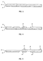
- FIG. 2 is a side view partly sectioned of the IC device adaptor element of Figure 1.
- IC device 10 is shown in abutting relation with heat spreader element 22.
- Back-up support elements 24 and 26 are also shown adjacent IC device 10. It can be seen how support elements 24 and 26 act as back-ups to adaptor element I/O pads 32 and pads 28, respectively.
- Flexible substrate 20 is shown bent around three sides of IC device 10.
- IC device I/O pads 12 are shown wire bonded to adaptor element pads 28 by wires 36.
- I/O pads 32 can typically be configured as controlled collapse chip connection (C4 type) interconnection points.
- C4 type controlled collapse chip connection
- Pads 12 of IC device 10 may also have a C4 type solder ball connection placed thereon such that IC device 10 can be directly mounted on a printed circuit board, or the like.
- IC device 10 can be directly mounted on a printed circuit board, or the like.
- C4 type solder ball connection placed thereon such that IC device 10 can be directly mounted on a printed circuit board, or the like.
- a description of the fabrication process for making the adaptor element illustrated in Figures 1 and 2 will now be described with reference to Figures 3-5.
- a polymer film such as a polyimide material is used for the flexible substrate 20 as shown in Figure 3 partly in cross-section.
- a stiffener layer 21 is then attached to one side of the polymer layer 20 by lamination, bonding or the like.
- the material of layer 21 may be any one of several thermally conductive materials e.g. metals.
- a copper layer 31 is also placed adjacent polyimide layer 20 on the side opposite stiffener layer 21 to form the substrate shown in cross-section in Figure 3.
- Stiffener layer 21 is then etched to form three distinct elements, i.e. heat spreader element 22 and back-up elements 24 and 26.
- the copper layer 31 is etched to form the circuit or signal lines 30 as shown in Figures 5 and 6. Etching is a well known technique wherein caustic solutions are used to remove that portion of a material which is unnecessary such that the required portions remain.
- joining metal is placed near one end of the assembly to form pads 28. C4 type solder balls are then formed on substantially the opposite ends of the signal lines 30.
- the joining metal that will make up pads 28 may be gold or nickel and pads 32 will likely be made from a tin/lead solder or the like, as is known in the art.
- signal lines 30 on the surface of flexible substrate 20 can be used to form the adaptor element being described.
- pattern plating may be used wherein a conductive seed layer is sputtered onto substrate layer 20 and circuit lines 30 are then selectively plated thereon in the desired locations through a dielectric mask. The dielectric mask is removed by washing, or the like, and the seed layer is subsequently removed by flash etching, thereby leaving circuit lines 30 in desired locations on the surface of flexible substrate 20.
- Figure 6 is a perspective view of the adaptor element shown in Figure 5, prior to its placement around an integrated circuit device 10.
- Flexible substrate 20 is shown having pads 28 and circuit lines 30 formed thereon. Additionally, connection pads 32 are shown electrically connected to pads 28 through lines 30.
- Heat spreader element 22 and the back-up elements 24 and 26 are also shown attached to flexible substrate layer 20. Wing portions 34 can be seen which will be used to connect and align the IC device 10 and adaptor element assembly on a printed circuit board, as described below with reference to Figure 8.
- the back-up element 24 is placed along one edge of IC device 10 as shown by arrow 42 and then bonded thereto by conventional means such as gluing, or the like.
- back-up element 26 is placed over portion 40 of IC device 10, as shown by arrow 44, and bonded thereto.
- the width of the adaptor element is designed so as not to cover any IC device I/O pads 12 and to directly correspond to area 40 of IC device 10.
- the configuration of the adaptor element can be changed according to the configuration of I/O pads on the IC device 10 being used.
- the width thereof is regulated by cutting, stamping, or the like an element having the desired dimensions from a sheet of substrate such as shown in Figures 3-5.
- heat spreader element 22 is then bent around adjacent to the side of IC device 10 opposite I/O pads 12 and bonded thereto, as shown by arrow 46.
- Pads 12 can then be electrically interconnected with pads 28 by techniques such as wire bonding, or the like.
- an assembly of an adaptor element and IC device which effectively re-positions the IC device I/O pads from one face of the IC device to a single edge of the IC device, thereby enhancing connectability of the IC device 10 in high density packaging applications, is shown.
- the bonding material may be chosen to electrically insulate support elements 22, 24, 26 from the surface of IC device 10 in order to prevent any potential electrical short circuits from occurring between IC device I/O pads.
- an electrically conductive bonding material can be used if the support elements are to be used as a ground plane, or the like.
- FIG 8 is an application of the adaptor element described wherein a printed circuit board 49 is shown with a high density packaging mounting assembly 50 affixed thereto.
- the IC device and adaptor element assemblies are held in place on board 49 by the mounting assembly 50 when the wing portions 34 of each adaptor element are slid into corresponding grooved portions 52 of the mounting assembly 50 as shown by arrow 51.
- Connection pads 54 are formed on the surface of board 49 and are in electrical connection with connectors 56 formed on the edge of board 49.
- Connection pads 54 will correspond in position with solder I/O pads 32 of the adaptor element such that when card 49 is plugged into a computer printed circuit board, or the like, a central processing unit is capable of communicating with IC device 10 through connectors 56, card pads 54, solder I/O pads 32, signal lines 30, connection pads 28, wire bonded lines 36 and IC device I/O pads 12.
- FIG. 9 Basically, the following embodiments will describe an adaptor element capable of being electrically connected to IC device 10 without the need for using wire bonding technology.
- the adaptor element of Figure 9 is fabricated similarly to the adaptor element fabricated by the process described with reference to Figures 3-5. However, subsequent to the formation of the signal lines 30 on flexible substrate layer 20, the end portion of polymer carrier layer 20 adjacent to lines 30 is removed such that the circuit lines 30 extend past the end of layer 20.
- These circuit line extensions 33 are flexible and are then attached to the I/O pads 12 of IC device 10 by techniques commonly used in tape automated bonding (TAB) technology, e.g. hot bar reflow, ultra sonic welding, thermal welding, or the like.
- TAB tape automated bonding
- the flexible polymer substrate 20 is shown disposed around IC device 10 having only a heat spreader element 22 and a back-up element 24 adjacent IC device 10. It can be seen that two signal layers are present one on each side of substrate 20. Circuit lines 30 and C4 type I/O pads 32 are present and extend along the outside of flexible substrate layer 20. Inner circuit lines 60 are shown on the inside of layer 20 and extend a sufficient distance to overlap and align with outer circuit lines 30. Vias or holes 64 are formed through both sets of circuit lines 30, 60 and polymer layer 20. Electrical conductive material 66 is then placed around the annulus of each via 64 by plating, electrodeposition, or the like.
- circuit lines 60 are in electrical connection with corresponding ones of circuit lines 30 through the electrically conductive annulus 66 of each via 64.
- vias 64 can be formed in lines 30, 60 and layer 20 by means known in the art such as laser ablation, punching, drilling, chemical etching, or the like.
- C4 type solder balls 62 are placed either on IC device I/O pads 20, or on inner circuit lines 60. Pads 12 and corresponding circuit lines 60 are then aligned and pressed together with C4 type solder balls 62 intermediate therebetween.
- methods other than C4 type technology can be used to join the adaptor element (circuit lines 60) with I/O pads 12, such as pad-to-pad joining techniques using appropriate joining metals.
- FIG. 11 Another embodiment of the present invention is shown in Figure 11, wherein a single signal plane adaptor element is used. Again, flexible substrate 20 is shown with heat spreader element 22 and back-up element 24 attached thereto and adjacent the IC device 10. Circuit lines 30 are formed as previously described along the outside of layer 20 and extend to the end thereof, as shown in Figure 11. Vias 70 are formed within layer 20 and filled with electrically conductive material 72. In a preferred embodiment vias 70 are in fact a pattern of holes corresponding to the IC device I/O pads 12 and are laser ablated or chemically removed from polymer carrier layer 20 directly beneath circuit lines 30 of the adaptor element. That is, the vias are formed after circuit lines 30 are placed on flexible substrate 20.
- the appropriate joining metal 72 such as solder or the like, is then plated or otherwise disposed in each via 72.
- C4 type joining technology can be used as shown by pads 62 to electrically connect IC device I/O pads 12 with joining metal 72 of each via 70.
- electrical connection is made from IC device I/O pads 12 through C4 type pads 62, metal 72 in each via 70, circuit lines 30 to corresponding adaptor I/O pads 32.
- substrate 20 can also be prepunched with vias 70 and the foil layer 31 subsequently bonded thereto ( Figure 3). However, when using this technique the bonding material, e.g. epoxy, enters vias 70 and must be removed prior to placing conductive material 72 therein.
- Figure 12 shows flexible layer 20 with heat spreader element 22 and back-up element 24 attached thereto and adjacent to IC device 10.
- layer 20 is extended a sufficient distance such that the adaptor element can be wrapped around and the circuit lines 30 on the outside thereof will now be adjacent to I/O pads 12 of IC device 10.
- a single signal plane adaptor element can be fabricated as described previously and appropriate joining metal, such as C4 type pads 62, can be placed on circuit lines 30 such that when the adaptor element is wrapped around the IC device they will correspond to I/O pads 12 on IC device 10.
- C4 type pads 62 can be placed on pads 12 such that when the adaptor element is wrapped around the IC device and circuit lines 30 are adjacent to I/O pads 12, pads 62 will be aligned with the corresponding circuit lines 30. In this manner, it can be seen that IC device I/O pads 12 are connected to corresponding ones of adaptor element I/O pads 32 through C4 type pads 62 and corresponding circuit lines 30.
- the adaptor element described is capable of effectively repositioning the I/O pads or contact points of an integrated circuit device 10 such that the IC device I/O pads are effectively aligned along the edge of the IC device/adaptor element assembly.
- high density packaging of integrated circuits is possible using I/C devices having differently configured I/O contact points.
- the present invention is particular useful in high density memory packaging, but it not limited thereto and is applicable to any type of IC device packaging wherein the original IC device I/O contact points must effectively be repositioned.
Abstract
The present invention relates to an adaptor element (20), for attachment to an electrical component (10) including at least one input/output contact point, comprising a body member (20, 22, 24, 26) adapted to be attached to the surface of the electrical component, at least one first type of contact (28) on the body member and adapted to be electrically connected to the input/output contact point (12) on the electrical component, and at least one second type of contact (32) on the body member, electrically connected to the first type of contact (28), and providing an input/output contact point for the adaptor element.
According to the invention the adaptor element is characterised in that the second type of contact (32) is spaced apart from the first type of component and the first type of contact is electrically connected to the input/output contact point on the electrically component, the second type of contact acts as an input/output contact point for the electrical component which is spaced apart from the input/output contact point on the electrical component.
Description
- This invention generally relates to connecting integrated electrical components such as circuit (IC) devices into an electrical circuit, for example, a computer system. In particular, an adaptor element is provided such that electrical connections between the input/output (I/O) contact points on an electrical component can effectively be re-positioned as required, thereby allowing different electrical interconnection configurations.
- Generally, IC devices are placed flat in an electrical circuit, i.e. the largest surface is placed on a planar printed circuit board. More specifically, the major plane of the IC device lies parallel with the plane of the circuit board on which the IC device is mounted. These integrated circuit devices are then electrically connected to the circuitry on the board by using known methods, such as wire bonding or direct chip attach (DCA) technology. Additionally packaged IC devices using surface mount technology (SMT) or pin-through-hole (PTH) technology are also placed flat on the printed circuit board and then electrically attached thereto.
- Adaptor elements for attaching IC devices to substrates on printed circuit boards are known. IBM Technical Disclosure Bulletin "Transmission Line Right Angle Connector" Vol. 26 No. 12 May 1984 page 6592 shows an interposer or adaptor element 3, having matching wiring, disposed between perpendicular IC device carriers 1, 2. US -A- 5,050,039 describes an IC device mounting arrangement wherein IC devices are attached, on one side, to a heat sink and the I/O contact points of the device are connected to vertically disposed interconnect boards. A flexible circuit is used to connect the interconnect boards to a motherboard.
- Additionally, it is known to mount perpendicularly, with reference to a corresponding substrate, a plurality of IC devices on a support member, as shown in US -A- 4,982,264 and US -A- 5,059,557. In these arrangements electrical conductors are disposed on a surface of the support member to contact bonding pads located on the IC device. Further, IC devices can be mounted perpendicularly with respect to a substrate in a "free standing" configuration. US -A- 4,922,378 and US -A- 5,031,072 describe a base plate having channels therein for supporting perpendicularly mounted integrated circuit devices. The IC devices are electrically interconnected to the base plate through pads on each IC device and the base plate. The base plate and IC device assembly is then electrically interconnected to an underlying planar surface by interconnecting a plurality of baseboard pads and connector pads. IBM Technical Disclosure Bulletin "Vertical Chip Packaging" Vol. 20, No. 11A, April 1978, page 4339 discloses mounting IC devices perpendicularly on a substrate. The IC devices are either placed in a channel in the substrate, or supported by a foil "foot" bonded to the back of each IC device. The foot can also be used to supply electrical power to the IC device. Foil "fingers" are then used to electrically interconnect the IC device I/O contact points to the substrate. It can be seen that conventional perpendicular IC device mounting requires placement of I/O contact points at specific locations on the IC device. In known arrangements, this placement of I/O contact points occurs at the IC device fabrication level and requires custom made IC devices be acquired from IC device manufacturers. Of course, a great deal of packaging flexibility is lost if specific IC devices must be special ordered from the manufacturer. Further, availability problems may also exist if standard "off the shelf" types of IC devices cannot be purchased and used in the desired packaging configuration. Therefore, it would be advantageous to provide an adaptor element which will allow any type of IC device to meet the desired packaging configuration.
- The object of the present invention is to provide an improved adaptor element for use with an electrical component which effectively re-positions the input/output contact points of the electrical component and to provide a combination of an electrical component formed with at least one input/out contact point and an adaptor element of the above type.
- The present invention relates to an adaptor element, for attachment to an electrical component including at least one input/output contact point, comprising a body member adapted to be attached to the surface of the electrical component, at least one first type of contact on the body member and adapted to be electrically connected to the input/output contact point on the electrical component, and at least one second type of contact on the body member, electrically connected to the first type of contact, and providing an input/output contact point for the adaptor element.
- According to the invention the adaptor element is characterised in that the second type of contact is spaced apart from the first type of contact, whereby, when the adaptor element is attached to the electrical component and the first type of contact is electrically connected to the input/output contact point on the electrical component, the second type of contact acts as an input/output contact point for the electrical component which is spaced apart from the input/output contact point on the electrical component.
- According to another aspect the present invention relates to the combination of an electrical component including at least one input/output contact point and an adaptor element, in which the adaptor element comprises a body member attached to the surface of the electrical component, at least one first type of contact on the body member and electrically connected to the input/output contact point on the electrical component, and at least one second type of contact on the body member, electrically connected to the first type of contact, and providing an input/output contact point for the adaptor element.
- According to the invention the combination is characterised in that the second type of contact is spaced apart from the first type of contact so that the second type of contact acts as an input/output contact point for the electrical component which is spaced apart from the input/output contact point on the electrical component.
- According to a preferred embodiment of the invention the electrical component is an integrated circuit device.
- In order that the invention may be more readily understood embodiments will now be described with reference to the accompanying drawings, in which:
- Figure 1 is a perspective view of an IC device with an adaptor element in accordance with one embodiment of the present invention,
- Figure 2 is a plan view of the assembly of Figure 1 wherein wirebonding is used to attach the IC device I/O contact points to the adaptor element,
- Figure 3 shows materials which can be used to fabricate the adaptor element of Figure 1,
- Figure 4 illustrates a first step in the fabrication process of the adaptor element of Figure 1,
- Figure 5 is a cross-sectional view of the fabricated adaptor element,
- Figure 6 is a perspective view of the adaptor element prior to its attachment to an IC device,
- Figure 7 is another perspective view of the adaptor element showing its attachment to an IC device,
- Figure 8 illustrates how an IC device with the adaptor element of Figure 1 can be incorporated into a module for attachment to a printed circuit board,
- Figure 9 is another embodiment of the present invention wherein the electrical connection between the IC device and the adaptor element is made using tape automated bonding techniques,
- Figure 10 is yet another embodiment of the present invention in which the adaptor element has two signal planes and an electrical connection between the IC device and the adaptor element is made through the annulus of a via (hole),
- Figure 11 is a further embodiment of the present invention in which the adaptor element has a single signal plane interconnected to the IC device through a metallized via (hole), and
- Figure 12 is a still further embodiment in which the adaptor element is elongated and includes a single circuit layer bent back on itself to interconnect with the IC device.
- Referring to Figure 1, a perspective view of an IC device adaptor element in accordance with the present invention is shown. An integrated circuit (IC)
device 10 is shown having a plurality of electrical connection input/output (I/O)contact points 12 on a surface thereof.IC device 10 may be one of any number of commercially available IC devices, such as dynamic random access memory (DRAM) devices, static random access memory (SRAM) devices, as well as any number of logic IC devices, and the like. It should be noted thatIC device 10 is a standard unpackaged integrated circuit wherein I/O contact points 12 are formed on the IC device in any number of different configurations and with different metals thereon depending on the packaging application, e.g. wire bonding. No new processing is required during the fabrication ofIC device 10 in order for it to be compatible with the adaptor element. - The adaptor element includes a
flexible substrate layer 20 which extends around three sides of the IC device and has three distinct metal elements thereon. A heat spreader and stiffeningelement 22 is shown adjacent the side ofIC device 10 opposite I/O contact points orpads 12. Abackup element 24 is used to support input/output (I/O)connection pads 32 on the adaptor element. Similarly, anotherbackup element 26 is used to supportbonding pads 28 andsignal lines 30 which extend to the I/O pads 32. It can be seen thatflexible substrate 20 with thediscrete metal elements IC device 10. It should be noted thatheat spreader element 22 and the adjacent portion ofsubstrate 20form wing portions 34 that extend past the ends ofIC device 10. Thesewing portions 34 can be used to insert the adaptor element and the IC device into a mounting assembly, as shown in Figure 8 and discussed in more detail below.Pads 28 andsignal lines 30 are disposed on the surface offlexible substrate 20opposite support members Pads 28 are covered with a joining metal, such as gold or nickel, by plating, sputtering or the like, to aid in the attachment ofwires 36.Wires 36 are used to attachIC device pads 12 withadaptor element pads 28 using wire bonding technology as is known in the art.Signal lines 30 electrically interconnectpads 28 and I/O pads 32 such thatIC device pads 12 are electrically connected withadaptor element pads 32, thereby effectively moving the positions of the I/O contact points ofIC device 10. - Figure 2 is a side view partly sectioned of the IC device adaptor element of Figure 1.
IC device 10 is shown in abutting relation withheat spreader element 22. Back-upsupport elements adjacent IC device 10. It can be seen howsupport elements O pads 32 andpads 28, respectively.Flexible substrate 20 is shown bent around three sides ofIC device 10. IC device I/O pads 12 are shown wire bonded toadaptor element pads 28 bywires 36. Circuit orsignal lines 30, formed on the outside ofsubstrate 20, electrically interconnectpads 28 with I/O pads 32. I/O pads 32 can typically be configured as controlled collapse chip connection (C4 type) interconnection points.Pads 12 ofIC device 10 may also have a C4 type solder ball connection placed thereon such thatIC device 10 can be directly mounted on a printed circuit board, or the like. Thus, the usefulness of the adaptor element can be seen since conventional direct attachment forIC device 10 will require a larger amount of a printed circuit board to be covered, or displaced, than by edge mountingIC device 10 having C4 type connections disposed along the narrow edge thereof. Those skilled in this particular art will understand that C4 type technology is well known and as such will not be described further herein. - A description of the fabrication process for making the adaptor element illustrated in Figures 1 and 2 will now be described with reference to Figures 3-5. A polymer film such as a polyimide material is used for the
flexible substrate 20 as shown in Figure 3 partly in cross-section. Astiffener layer 21 is then attached to one side of thepolymer layer 20 by lamination, bonding or the like. The material oflayer 21 may be any one of several thermally conductive materials e.g. metals. Acopper layer 31 is also placedadjacent polyimide layer 20 on the side oppositestiffener layer 21 to form the substrate shown in cross-section in Figure 3.Stiffener layer 21 is then etched to form three distinct elements, i.e.heat spreader element 22 and back-upelements layer 21, thecopper layer 31 is etched to form the circuit orsignal lines 30 as shown in Figures 5 and 6. Etching is a well known technique wherein caustic solutions are used to remove that portion of a material which is unnecessary such that the required portions remain. Subsequent to the formation oflines 30 on theflexible substrate 20, joining metal is placed near one end of the assembly to formpads 28. C4 type solder balls are then formed on substantially the opposite ends of the signal lines 30. The joining metal that will make uppads 28 may be gold or nickel andpads 32 will likely be made from a tin/lead solder or the like, as is known in the art. Additionally, it should be noted that other techniques of formingsignal lines 30 on the surface offlexible substrate 20 can be used to form the adaptor element being described. For example, pattern plating may be used wherein a conductive seed layer is sputtered ontosubstrate layer 20 andcircuit lines 30 are then selectively plated thereon in the desired locations through a dielectric mask. The dielectric mask is removed by washing, or the like, and the seed layer is subsequently removed by flash etching, thereby leavingcircuit lines 30 in desired locations on the surface offlexible substrate 20. - Figure 6 is a perspective view of the adaptor element shown in Figure 5, prior to its placement around an
integrated circuit device 10.Flexible substrate 20 is shown havingpads 28 andcircuit lines 30 formed thereon. Additionally,connection pads 32 are shown electrically connected topads 28 throughlines 30.Heat spreader element 22 and the back-upelements flexible substrate layer 20.Wing portions 34 can be seen which will be used to connect and align theIC device 10 and adaptor element assembly on a printed circuit board, as described below with reference to Figure 8. - Placement of the adaptor element described around an integrated circuit device will now be described with reference to Figure 7. First, the back-up
element 24 is placed along one edge ofIC device 10 as shown byarrow 42 and then bonded thereto by conventional means such as gluing, or the like. Subsequently, back-upelement 26 is placed overportion 40 ofIC device 10, as shown byarrow 44, and bonded thereto. It should be noted that the width of the adaptor element is designed so as not to cover any IC device I/O pads 12 and to directly correspond toarea 40 ofIC device 10. The configuration of the adaptor element can be changed according to the configuration of I/O pads on theIC device 10 being used. During fabrication of the adaptor element, the width thereof is regulated by cutting, stamping, or the like an element having the desired dimensions from a sheet of substrate such as shown in Figures 3-5. Subsequent to bonding of the back-upelement 26 toIC device 10heat spreader element 22 is then bent around adjacent to the side ofIC device 10 opposite I/O pads 12 and bonded thereto, as shown byarrow 46.Pads 12 can then be electrically interconnected withpads 28 by techniques such as wire bonding, or the like. Thus, an assembly of an adaptor element and IC device which effectively re-positions the IC device I/O pads from one face of the IC device to a single edge of the IC device, thereby enhancing connectability of theIC device 10 in high density packaging applications, is shown. It should be noted that the bonding material may be chosen to electrically insulatesupport elements IC device 10 in order to prevent any potential electrical short circuits from occurring between IC device I/O pads. Alternatively, an electrically conductive bonding material can be used if the support elements are to be used as a ground plane, or the like. - Figure 8 is an application of the adaptor element described wherein a printed
circuit board 49 is shown with a high densitypackaging mounting assembly 50 affixed thereto. The IC device and adaptor element assemblies are held in place onboard 49 by the mountingassembly 50 when thewing portions 34 of each adaptor element are slid into correspondinggrooved portions 52 of the mountingassembly 50 as shown byarrow 51. Connection pads 54 are formed on the surface ofboard 49 and are in electrical connection withconnectors 56 formed on the edge ofboard 49. Connection pads 54 will correspond in position with solder I/O pads 32 of the adaptor element such that whencard 49 is plugged into a computer printed circuit board, or the like, a central processing unit is capable of communicating withIC device 10 throughconnectors 56, card pads 54, solder I/O pads 32,signal lines 30,connection pads 28, wire bondedlines 36 and IC device I/O pads 12. - Other embodiments of the present invention will now be described beginning with reference to Figure 9. Basically, the following embodiments will describe an adaptor element capable of being electrically connected to
IC device 10 without the need for using wire bonding technology. The adaptor element of Figure 9 is fabricated similarly to the adaptor element fabricated by the process described with reference to Figures 3-5. However, subsequent to the formation of the signal lines 30 onflexible substrate layer 20, the end portion ofpolymer carrier layer 20 adjacent tolines 30 is removed such that thecircuit lines 30 extend past the end oflayer 20. Thesecircuit line extensions 33 are flexible and are then attached to the I/O pads 12 ofIC device 10 by techniques commonly used in tape automated bonding (TAB) technology, e.g. hot bar reflow, ultra sonic welding, thermal welding, or the like. Thus, it can be seen how the adaptor element can be affixed toIC device 10 and electrically connected thereto using TAB technology rather than the wire bonding described with reference to Figures 1-8. - Referring to Figure 10, the
flexible polymer substrate 20 is shown disposed aroundIC device 10 having only aheat spreader element 22 and a back-upelement 24adjacent IC device 10. It can be seen that two signal layers are present one on each side ofsubstrate 20.Circuit lines 30 and C4 type I/O pads 32 are present and extend along the outside offlexible substrate layer 20.Inner circuit lines 60 are shown on the inside oflayer 20 and extend a sufficient distance to overlap and align with outer circuit lines 30. Vias or holes 64 are formed through both sets ofcircuit lines polymer layer 20. Electricalconductive material 66 is then placed around the annulus of each via 64 by plating, electrodeposition, or the like. Thus, it can be seen that circuit lines 60 are in electrical connection with corresponding ones ofcircuit lines 30 through the electricallyconductive annulus 66 of each via 64. It should be noted thatvias 64 can be formed inlines layer 20 by means known in the art such as laser ablation, punching, drilling, chemical etching, or the like. Next, C4type solder balls 62 are placed either on IC device I/O pads 20, or on inner circuit lines 60.Pads 12 andcorresponding circuit lines 60 are then aligned and pressed together with C4type solder balls 62 intermediate therebetween. Of course, methods other than C4 type technology can be used to join the adaptor element (circuit lines 60) with I/O pads 12, such as pad-to-pad joining techniques using appropriate joining metals. Subsequent to the connection of I/O pads 12 withcircuit lines 60 it can be seen how IC device I/O pads 12 are now in electrical connection with corresponding adaptor I/O pads 32 throughinner circuit lines 60, through each viaannulus 66 and outer circuit lines 30. - Another embodiment of the present invention is shown in Figure 11, wherein a single signal plane adaptor element is used. Again,
flexible substrate 20 is shown withheat spreader element 22 and back-upelement 24 attached thereto and adjacent theIC device 10.Circuit lines 30 are formed as previously described along the outside oflayer 20 and extend to the end thereof, as shown in Figure 11.Vias 70 are formed withinlayer 20 and filled with electricallyconductive material 72. In apreferred embodiment vias 70 are in fact a pattern of holes corresponding to the IC device I/O pads 12 and are laser ablated or chemically removed frompolymer carrier layer 20 directly beneathcircuit lines 30 of the adaptor element. That is, the vias are formed aftercircuit lines 30 are placed onflexible substrate 20. The appropriate joiningmetal 72, such as solder or the like, is then plated or otherwise disposed in each via 72. Again, C4 type joining technology can be used as shown bypads 62 to electrically connect IC device I/O pads 12 with joiningmetal 72 of each via 70. In this embodiment electrical connection is made from IC device I/O pads 12 throughC4 type pads 62,metal 72 in each via 70,circuit lines 30 to corresponding adaptor I/O pads 32. It should be noted thatsubstrate 20 can also be prepunched withvias 70 and thefoil layer 31 subsequently bonded thereto (Figure 3). However, when using this technique the bonding material, e.g. epoxy, entersvias 70 and must be removed prior to placingconductive material 72 therein. - Figure 12 shows
flexible layer 20 withheat spreader element 22 and back-upelement 24 attached thereto and adjacent toIC device 10. In the embodiment of Figure 12,layer 20 is extended a sufficient distance such that the adaptor element can be wrapped around and the circuit lines 30 on the outside thereof will now be adjacent to I/O pads 12 ofIC device 10. Thus, a single signal plane adaptor element can be fabricated as described previously and appropriate joining metal, such asC4 type pads 62, can be placed oncircuit lines 30 such that when the adaptor element is wrapped around the IC device they will correspond to I/O pads 12 onIC device 10. Alternatively,C4 type pads 62 can be placed onpads 12 such that when the adaptor element is wrapped around the IC device andcircuit lines 30 are adjacent to I/O pads 12,pads 62 will be aligned with the corresponding circuit lines 30. In this manner, it can be seen that IC device I/O pads 12 are connected to corresponding ones of adaptor element I/O pads 32 throughC4 type pads 62 and corresponding circuit lines 30. - It can be seen that the adaptor element described is capable of effectively repositioning the I/O pads or contact points of an
integrated circuit device 10 such that the IC device I/O pads are effectively aligned along the edge of the IC device/adaptor element assembly. In this manner, high density packaging of integrated circuits is possible using I/C devices having differently configured I/O contact points. The present invention is particular useful in high density memory packaging, but it not limited thereto and is applicable to any type of IC device packaging wherein the original IC device I/O contact points must effectively be repositioned.
Claims (10)
- An adaptor element (20), for attachment to an electrical component (10) including at least one input/output contact point (12), comprising
a body member (20, 22, 24, 26) adapted to be attached to the surface of said electrical component, and
at least one second type of contact (32) on said body member, electrically connected to said first type of contact (28), and providing an input/output contact point for said adaptor element,
characterised in that
said second type of contact (32) is spaced apart from said first type of contact (28),
whereby,
when said adaptor element is attached to said electrical component and said first type of contact is electrically connected to said input/output contact point on said electrical component, said second type of contact acts as an input/output contact point for said electrical component which is spaced apart from said input/output contact point on said electrical component. - An adaptor element as claimed in Claim 1 characterised in that said first type of contact and said second type of contact are positioned on said body member in such a way that, when said adaptor element is attached to said electrical component, said first type of contact and said second type of contact are positioned adjacent to two different surfaces of said electrical component.
- An adaptor element as claimed in Claim 2 characterised in that said body member has two portions extending substantially at right angles to one another, said first type of contact is positioned on one of said body portions, and said second type of contact is positioned on the other of said body portions.
- An adaptor element as claimed in Claim 2 characterised in that said body member is substantially U-shaped and is adapted to fit closely to three surfaces of said electrical component.
- An adaptor element as claimed in any one of the preceding claims characterised in that said body member comprises a flexible portion (20) and stiffener elements (24, 26) attached to said flexible portion adjacent to said contacts.
- The combination of an electrical component (10 including at least one input/output contact point (12) and an adaptor element (20),
in which said adaptor element comprises
a body member (20, 22, 24, 26) attached to the surface of said electrical component,
at least one first type of contact (28) on said body member and electrically connected to said input/output contact point (12) on said electrical component, and
at least one second type of contact (32) on said body member, electrically connected to said first type of contact (28), and providing an input/output contact point for said adaptor element,
characterised in that
said second type of contact is spaced apart from said first type of contact so that said second type of contact acts as an input/output contact point for said electrical component which is spaced apart from said input/output contact point on said electrical component. - A combination as claimed in Claim 6 characterised in that said first type of contact and said second type of contact are positioned on said body member in such a way that said first type of contact and said second type of contact are positioned adjacent to two different surfaces of said electrical component.
- A combination as claimed in Claim 7 characterised in that said body member has two portions extending substantially at right angles to one another, said first type of contact is positioned on one of said body portions, and said second type of contact is positioned on the other of said body portions.
- A combination as claimed in Claim 8 characterised in that said body member is substantially U-shaped and fits closely to three surfaces of said electrical component.
- A combination as claimed in any one of the preceding claims 6 to 9 characterised in that said electrical component (10) is an integrated circuit device.
Applications Claiming Priority (2)
| Application Number | Priority Date | Filing Date | Title |
|---|---|---|---|
| US07/846,301 US5229916A (en) | 1992-03-04 | 1992-03-04 | Chip edge interconnect overlay element |
| US846301 | 1997-04-30 |
Publications (2)
| Publication Number | Publication Date |
|---|---|
| EP0562725A2 true EP0562725A2 (en) | 1993-09-29 |
| EP0562725A3 EP0562725A3 (en) | 1993-10-06 |
Family
ID=25297495
Family Applications (1)
| Application Number | Title | Priority Date | Filing Date |
|---|---|---|---|
| EP19930301514 Withdrawn EP0562725A3 (en) | 1992-03-04 | 1993-02-26 | Adaptor element for modifying electrical connections to an electrical component |
Country Status (3)
| Country | Link |
|---|---|
| US (1) | US5229916A (en) |
| EP (1) | EP0562725A3 (en) |
| JP (1) | JP2525110B2 (en) |
Cited By (4)
| Publication number | Priority date | Publication date | Assignee | Title |
|---|---|---|---|---|
| WO1998019863A1 (en) * | 1996-11-08 | 1998-05-14 | W.L. Gore & Associates, Inc. | Method and apparatus for aligning and laminating substrates to stiffeners in electrical circuits |
| EP0849795A2 (en) * | 1996-12-17 | 1998-06-24 | Lsi Logic Corporation | Adhesive promotion of TAB/FLEX tape in a laminar electronic package contruction |
| CN1073746C (en) * | 1995-12-15 | 2001-10-24 | 国际商业机器公司 | Controlled profile multiple chip modules |
| WO2005101490A2 (en) * | 2004-04-19 | 2005-10-27 | Siemens Aktiengesellschaft | Component that is situated on a cooling fin |
Families Citing this family (96)
| Publication number | Priority date | Publication date | Assignee | Title |
|---|---|---|---|---|
| US5375041A (en) * | 1992-12-02 | 1994-12-20 | Intel Corporation | Ra-tab array bump tab tape based I.C. package |
| US5375321A (en) * | 1993-03-30 | 1994-12-27 | United States Department Of Energy | Method for fabricating fan-fold shielded electrical leads |
| US5602419A (en) * | 1993-12-16 | 1997-02-11 | Nec Corporation | Chip carrier semiconductor device assembly |
| JPH07312469A (en) * | 1994-05-16 | 1995-11-28 | Nippon Mektron Ltd | Structure of bent part of multilayer flexible circuit board |
| DE4426465A1 (en) * | 1994-07-26 | 1996-02-01 | Siemens Ag | Connection part between electrical connections inside a housing and connections protruding from the housing |
| US5434362A (en) * | 1994-09-06 | 1995-07-18 | Motorola, Inc. | Flexible circuit board assembly and method |
| JP2570628B2 (en) * | 1994-09-21 | 1997-01-08 | 日本電気株式会社 | Semiconductor package and manufacturing method thereof |
| JPH11505957A (en) | 1995-05-26 | 1999-05-25 | ランバス・インコーポレーテッド | Chip socket assembly and chip file assembly for semiconductor chips |
| US20020055285A1 (en) * | 1999-12-20 | 2002-05-09 | Rambus, Inc. | Chip socket assembly and chip file assembly for semiconductor chips |
| US5680342A (en) * | 1996-04-10 | 1997-10-21 | International Business Machines Corporation | Memory module package with address bus buffering |
| US5706218A (en) * | 1996-05-15 | 1998-01-06 | Intel Corporation | Random number generator |
| US6881611B1 (en) * | 1996-07-12 | 2005-04-19 | Fujitsu Limited | Method and mold for manufacturing semiconductor device, semiconductor device and method for mounting the device |
| EP1189271A3 (en) * | 1996-07-12 | 2003-07-16 | Fujitsu Limited | Wiring boards and mounting of semiconductor devices thereon |
| US5891354A (en) * | 1996-07-26 | 1999-04-06 | Fujitsu Limited | Methods of etching through wafers and substrates with a composite etch stop layer |
| US5863812A (en) * | 1996-09-19 | 1999-01-26 | Vlsi Technology, Inc. | Process for manufacturing a multi layer bumped semiconductor device |
| US5903437A (en) * | 1997-01-17 | 1999-05-11 | International Business Machines Corporation | High density edge mounting of chips |
| US5818107A (en) * | 1997-01-17 | 1998-10-06 | International Business Machines Corporation | Chip stacking by edge metallization |
| US6002589A (en) | 1997-07-21 | 1999-12-14 | Rambus Inc. | Integrated circuit package for coupling to a printed circuit board |
| US6234820B1 (en) | 1997-07-21 | 2001-05-22 | Rambus Inc. | Method and apparatus for joining printed circuit boards |
| JP3294785B2 (en) * | 1997-09-01 | 2002-06-24 | シャープ株式会社 | Heat dissipation structure of circuit element |
| US6043558A (en) * | 1997-09-12 | 2000-03-28 | Micron Technology, Inc. | IC packages including separated signal and power supply edge connections, systems and devices including such packages, and methods of connecting such packages |
| US5917704A (en) * | 1997-10-06 | 1999-06-29 | Ford Motor Company | Laser-solderable electronic component |
| KR100499398B1 (en) * | 1997-12-31 | 2005-09-26 | 주식회사 하이닉스반도체 | Heat dissipation package and its manufacturing method |
| US6005776A (en) * | 1998-01-05 | 1999-12-21 | Intel Corporation | Vertical connector based packaging solution for integrated circuits |
| US6028365A (en) * | 1998-03-30 | 2000-02-22 | Micron Technology, Inc. | Integrated circuit package and method of fabrication |
| US5920462A (en) * | 1998-04-10 | 1999-07-06 | Ford Motor Company | Heat spreader mounting pad configurations for laser soldering |
| WO2000059033A1 (en) * | 1999-03-25 | 2000-10-05 | Seiko Epson Corporation | Wiring board, connection board, semiconductor device, method of manufacture thereof, circuit board, and electronic device |
| US6323060B1 (en) | 1999-05-05 | 2001-11-27 | Dense-Pac Microsystems, Inc. | Stackable flex circuit IC package and method of making same |
| JP3668066B2 (en) * | 1999-09-01 | 2005-07-06 | 富士通株式会社 | Printed wiring board for semiconductor package and manufacturing method thereof |
| US6262895B1 (en) | 2000-01-13 | 2001-07-17 | John A. Forthun | Stackable chip package with flex carrier |
| JP3495305B2 (en) * | 2000-02-02 | 2004-02-09 | Necエレクトロニクス株式会社 | Semiconductor device and semiconductor module |
| US6356458B1 (en) * | 2000-03-14 | 2002-03-12 | Lockheed Martin Corporation | Extreme density packaging for electronic assemblies |
| US6449159B1 (en) * | 2000-05-03 | 2002-09-10 | Rambus Inc. | Semiconductor module with imbedded heat spreader |
| US7122889B2 (en) * | 2000-05-03 | 2006-10-17 | Rambus, Inc. | Semiconductor module |
| US6833984B1 (en) | 2000-05-03 | 2004-12-21 | Rambus, Inc. | Semiconductor module with serial bus connection to multiple dies |
| DE10051884A1 (en) * | 2000-10-19 | 2002-04-25 | Cherry Gmbh | Process for the production of conductor foil carrier housing units |
| US6940729B2 (en) | 2001-10-26 | 2005-09-06 | Staktek Group L.P. | Integrated circuit stacking system and method |
| US20060255446A1 (en) | 2001-10-26 | 2006-11-16 | Staktek Group, L.P. | Stacked modules and method |
| US7026708B2 (en) * | 2001-10-26 | 2006-04-11 | Staktek Group L.P. | Low profile chip scale stacking system and method |
| US6956284B2 (en) | 2001-10-26 | 2005-10-18 | Staktek Group L.P. | Integrated circuit stacking system and method |
| US7202555B2 (en) | 2001-10-26 | 2007-04-10 | Staktek Group L.P. | Pitch change and chip scale stacking system and method |
| US6914324B2 (en) * | 2001-10-26 | 2005-07-05 | Staktek Group L.P. | Memory expansion and chip scale stacking system and method |
| US7656678B2 (en) | 2001-10-26 | 2010-02-02 | Entorian Technologies, Lp | Stacked module systems |
| US7053478B2 (en) | 2001-10-26 | 2006-05-30 | Staktek Group L.P. | Pitch change and chip scale stacking system |
| US20030234443A1 (en) | 2001-10-26 | 2003-12-25 | Staktek Group, L.P. | Low profile stacking system and method |
| US7310458B2 (en) | 2001-10-26 | 2007-12-18 | Staktek Group L.P. | Stacked module systems and methods |
| US7485951B2 (en) | 2001-10-26 | 2009-02-03 | Entorian Technologies, Lp | Modularized die stacking system and method |
| US7371609B2 (en) | 2001-10-26 | 2008-05-13 | Staktek Group L.P. | Stacked module systems and methods |
| EP1306898A1 (en) * | 2001-10-29 | 2003-05-02 | Dialog Semiconductor GmbH | Sub-milliohm on-chip interconnection |
| US7081373B2 (en) | 2001-12-14 | 2006-07-25 | Staktek Group, L.P. | CSP chip stack with flex circuit |
| US6721189B1 (en) * | 2002-03-13 | 2004-04-13 | Rambus, Inc. | Memory module |
| US7542304B2 (en) | 2003-09-15 | 2009-06-02 | Entorian Technologies, Lp | Memory expansion and integrated circuit stacking system and method |
| KR100564620B1 (en) * | 2004-03-31 | 2006-03-29 | 삼성전자주식회사 | Memory module, socket for memory module and mounting method using the same for improving a heat spread characteristics |
| US7254036B2 (en) * | 2004-04-09 | 2007-08-07 | Netlist, Inc. | High density memory module using stacked printed circuit boards |
| US20060053345A1 (en) * | 2004-09-03 | 2006-03-09 | Staktek Group L.P. | Thin module system and method |
| US7289327B2 (en) * | 2006-02-27 | 2007-10-30 | Stakick Group L.P. | Active cooling methods and apparatus for modules |
| US7443023B2 (en) | 2004-09-03 | 2008-10-28 | Entorian Technologies, Lp | High capacity thin module system |
| US7616452B2 (en) | 2004-09-03 | 2009-11-10 | Entorian Technologies, Lp | Flex circuit constructions for high capacity circuit module systems and methods |
| US7324352B2 (en) | 2004-09-03 | 2008-01-29 | Staktek Group L.P. | High capacity thin module system and method |
| US7468893B2 (en) | 2004-09-03 | 2008-12-23 | Entorian Technologies, Lp | Thin module system and method |
| US7446410B2 (en) | 2004-09-03 | 2008-11-04 | Entorian Technologies, Lp | Circuit module with thermal casing systems |
| US7522421B2 (en) * | 2004-09-03 | 2009-04-21 | Entorian Technologies, Lp | Split core circuit module |
| US20060050492A1 (en) | 2004-09-03 | 2006-03-09 | Staktek Group, L.P. | Thin module system and method |
| US7606050B2 (en) | 2004-09-03 | 2009-10-20 | Entorian Technologies, Lp | Compact module system and method |
| US7423885B2 (en) | 2004-09-03 | 2008-09-09 | Entorian Technologies, Lp | Die module system |
| US7542297B2 (en) * | 2004-09-03 | 2009-06-02 | Entorian Technologies, Lp | Optimized mounting area circuit module system and method |
| US7606040B2 (en) | 2004-09-03 | 2009-10-20 | Entorian Technologies, Lp | Memory module system and method |
| US7760513B2 (en) | 2004-09-03 | 2010-07-20 | Entorian Technologies Lp | Modified core for circuit module system and method |
| US7511968B2 (en) | 2004-09-03 | 2009-03-31 | Entorian Technologies, Lp | Buffered thin module system and method |
| US7606049B2 (en) | 2004-09-03 | 2009-10-20 | Entorian Technologies, Lp | Module thermal management system and method |
| US7579687B2 (en) | 2004-09-03 | 2009-08-25 | Entorian Technologies, Lp | Circuit module turbulence enhancement systems and methods |
| US7309914B2 (en) | 2005-01-20 | 2007-12-18 | Staktek Group L.P. | Inverted CSP stacking system and method |
| US7915744B2 (en) * | 2005-04-18 | 2011-03-29 | Mediatek Inc. | Bond pad structures and semiconductor devices using the same |
| US7033861B1 (en) | 2005-05-18 | 2006-04-25 | Staktek Group L.P. | Stacked module systems and method |
| US7442050B1 (en) * | 2005-08-29 | 2008-10-28 | Netlist, Inc. | Circuit card with flexible connection for memory module with heat spreader |
| US7576995B2 (en) | 2005-11-04 | 2009-08-18 | Entorian Technologies, Lp | Flex circuit apparatus and method for adding capacitance while conserving circuit board surface area |
| US7608920B2 (en) | 2006-01-11 | 2009-10-27 | Entorian Technologies, Lp | Memory card and method for devising |
| US7508058B2 (en) | 2006-01-11 | 2009-03-24 | Entorian Technologies, Lp | Stacked integrated circuit module |
| US7605454B2 (en) | 2006-01-11 | 2009-10-20 | Entorian Technologies, Lp | Memory card and method for devising |
| US7304382B2 (en) | 2006-01-11 | 2007-12-04 | Staktek Group L.P. | Managed memory component |
| US7508069B2 (en) | 2006-01-11 | 2009-03-24 | Entorian Technologies, Lp | Managed memory component |
| US7511969B2 (en) | 2006-02-02 | 2009-03-31 | Entorian Technologies, Lp | Composite core circuit module system and method |
| US7619893B1 (en) | 2006-02-17 | 2009-11-17 | Netlist, Inc. | Heat spreader for electronic modules |
| TW200803651A (en) * | 2006-06-02 | 2008-01-01 | Chicony Electronic Co Ltd | Method of fabricating electronic module with side contact |
| US7468553B2 (en) | 2006-10-20 | 2008-12-23 | Entorian Technologies, Lp | Stackable micropackages and stacked modules |
| JP4697118B2 (en) * | 2006-10-23 | 2011-06-08 | 株式会社デンソー | Electronic equipment |
| US7417310B2 (en) | 2006-11-02 | 2008-08-26 | Entorian Technologies, Lp | Circuit module having force resistant construction |
| KR100885976B1 (en) * | 2007-06-25 | 2009-03-03 | 삼성전자주식회사 | Printed circuit board, memory module having the same and fabrication method thereof |
| JP5115269B2 (en) | 2008-03-26 | 2013-01-09 | 日本電気株式会社 | Semiconductor device mounting structure and electronic device using the mounting structure |
| US8018723B1 (en) | 2008-04-30 | 2011-09-13 | Netlist, Inc. | Heat dissipation for electronic modules |
| US9312855B2 (en) * | 2012-01-10 | 2016-04-12 | Atmel Corporation | Touch sensor tracks |
| JP6112796B2 (en) | 2012-07-17 | 2017-04-12 | オリンパス株式会社 | Semiconductor device mounting structure |
| CN103247233B (en) * | 2013-04-28 | 2015-09-23 | 京东方科技集团股份有限公司 | Flexible base, board, display device and attach the method for electron device on flexible substrates |
| US11166373B2 (en) | 2018-10-09 | 2021-11-02 | Delta Electronics, Inc. | Voltage regulator module |
| US10973127B2 (en) | 2018-10-09 | 2021-04-06 | Delta Electronics, Inc. | Voltage regulator module |
| US11158451B2 (en) | 2018-10-09 | 2021-10-26 | Delta Electronics, Inc. | Power module |
Citations (1)
| Publication number | Priority date | Publication date | Assignee | Title |
|---|---|---|---|---|
| WO1992005582A1 (en) * | 1990-09-24 | 1992-04-02 | Tessera, Inc. | Semiconductor chip assemblies, methods of making same and components for same |
Family Cites Families (15)
| Publication number | Priority date | Publication date | Assignee | Title |
|---|---|---|---|---|
| US3766439A (en) * | 1972-01-12 | 1973-10-16 | Gen Electric | Electronic module using flexible printed circuit board with heat sink means |
| JPS556852A (en) * | 1978-06-28 | 1980-01-18 | Mitsubishi Electric Corp | Semiconductor device |
| JPS57193094A (en) * | 1981-05-18 | 1982-11-27 | Matsushita Electric Ind Co Ltd | Electronic circuit part and method of mounting same |
| JPS58189614A (en) * | 1982-04-29 | 1983-11-05 | Sharp Corp | Display panel |
| JPS6046040A (en) * | 1983-08-24 | 1985-03-12 | Nec Corp | Semiconductor device |
| JPS61121449A (en) * | 1984-11-19 | 1986-06-09 | Nippon Telegr & Teleph Corp <Ntt> | Mounting structure and process of lsi chip |
| US4982264A (en) * | 1985-02-27 | 1991-01-01 | Texas Instruments Incorporated | High density integrated circuit package |
| JPS62260341A (en) * | 1986-05-06 | 1987-11-12 | Mitsubishi Electric Corp | Forming method of multilayer interconnection layer |
| US4922378A (en) * | 1986-08-01 | 1990-05-01 | Texas Instruments Incorporated | Baseboard for orthogonal chip mount |
| US4858071A (en) * | 1987-02-24 | 1989-08-15 | Nissan Motor Co., Ltd. | Electronic circuit apparatus |
| US4855809A (en) * | 1987-11-24 | 1989-08-08 | Texas Instruments Incorporated | Orthogonal chip mount system module and method |
| US5040052A (en) * | 1987-12-28 | 1991-08-13 | Texas Instruments Incorporated | Compact silicon module for high density integrated circuits |
| US5059557A (en) * | 1989-08-08 | 1991-10-22 | Texas Instruments Incorporated | Method of electrically connecting integrated circuits by edge-insertion in grooved support members |
| US5040997A (en) * | 1990-06-08 | 1991-08-20 | The Foxboro Company | Flex circuit connector assembly and method for manufacturing the same |
| US5050039A (en) * | 1990-06-26 | 1991-09-17 | Digital Equipment Corporation | Multiple circuit chip mounting and cooling arrangement |
-
1992
- 1992-03-04 US US07/846,301 patent/US5229916A/en not_active Expired - Fee Related
-
1993
- 1993-01-26 JP JP5011147A patent/JP2525110B2/en not_active Expired - Lifetime
- 1993-02-26 EP EP19930301514 patent/EP0562725A3/en not_active Withdrawn
Patent Citations (1)
| Publication number | Priority date | Publication date | Assignee | Title |
|---|---|---|---|---|
| WO1992005582A1 (en) * | 1990-09-24 | 1992-04-02 | Tessera, Inc. | Semiconductor chip assemblies, methods of making same and components for same |
Non-Patent Citations (4)
| Title |
|---|
| ELECTRONICS. vol. 46, no. 7, 29 March 1973, NEW YORK US pages 86 - 91 M.A. BERGER ET AL. 'Flat, Flexible Cable Makes Excellent IC Interface' * |
| ELECTRONICS. vol. 47, no. 10, 16 May 1974, NEW YORK US pages 89 - 95 S.E. GROSSMAN 'Film-Carrier Technique Automates the Packaging of IC Chips' * |
| IBM TECHNICAL DISCLOSURE BULLETIN. vol. 32, no. 2, July 1989, NEW YORK US pages 262 - 265 'Edge-Connected TAB Memory Package' * |
| PATENT ABSTRACTS OF JAPAN vol. 12, no. 135 (E-604)(2982) 23 April 1988 & JP-A-62 260 343 ( MITSUBISHI ELECTRIC CORP ) * |
Cited By (7)
| Publication number | Priority date | Publication date | Assignee | Title |
|---|---|---|---|---|
| CN1073746C (en) * | 1995-12-15 | 2001-10-24 | 国际商业机器公司 | Controlled profile multiple chip modules |
| WO1998019863A1 (en) * | 1996-11-08 | 1998-05-14 | W.L. Gore & Associates, Inc. | Method and apparatus for aligning and laminating substrates to stiffeners in electrical circuits |
| US5882459A (en) * | 1996-11-08 | 1999-03-16 | W. L. Gore & Associates, Inc. | Method for aligning and laminating substrates to stiffeners in electrical circuits |
| EP0849795A2 (en) * | 1996-12-17 | 1998-06-24 | Lsi Logic Corporation | Adhesive promotion of TAB/FLEX tape in a laminar electronic package contruction |
| EP0849795A3 (en) * | 1996-12-17 | 1998-12-02 | Lsi Logic Corporation | Adhesive promotion of TAB/FLEX tape in a laminar electronic package contruction |
| WO2005101490A2 (en) * | 2004-04-19 | 2005-10-27 | Siemens Aktiengesellschaft | Component that is situated on a cooling fin |
| WO2005101490A3 (en) * | 2004-04-19 | 2006-04-13 | Siemens Ag | Component that is situated on a cooling fin |
Also Published As
| Publication number | Publication date |
|---|---|
| EP0562725A3 (en) | 1993-10-06 |
| JP2525110B2 (en) | 1996-08-14 |
| US5229916A (en) | 1993-07-20 |
| JPH06120285A (en) | 1994-04-28 |
Similar Documents
| Publication | Publication Date | Title |
|---|---|---|
| EP0562725A2 (en) | Adaptor element for modifying electrical connections to an electrical component | |
| EP0527044B1 (en) | Memory package | |
| EP0575806B1 (en) | Package for integrated circuit chips | |
| US5198965A (en) | Free form packaging of specific functions within a computer system | |
| US4567543A (en) | Double-sided flexible electronic circuit module | |
| EP0480754B1 (en) | Mounting device for mounting an electronic device on a substrate by the surface mounting technology | |
| US6493240B2 (en) | Interposer for connecting two substrates and resulting assembly | |
| US5239448A (en) | Formulation of multichip modules | |
| US5463191A (en) | Circuit board having an improved fine pitch ball grid array and method of assembly therefor | |
| US5424492A (en) | Optimal PCB routing methodology for high I/O density interconnect devices | |
| EP1705967B1 (en) | Off-grid decoupling capacitor of ball grid array (BGA) devices and method | |
| US6480014B1 (en) | High density, high frequency memory chip modules having thermal management structures | |
| US5613033A (en) | Laminated module for stacking integrated circuits | |
| US6603079B2 (en) | Printed circuit board electrical interconnects | |
| JPS62584B2 (en) | ||
| US6441486B1 (en) | BGA substrate via structure | |
| US5184284A (en) | Method and apparatus for implementing engineering changes for integrated circuit module | |
| US6691408B2 (en) | Printed circuit board electrical interconnects | |
| US7068120B2 (en) | Electromagnetic bus coupling having an electromagnetic coupling interposer | |
| US5938454A (en) | Electrical connector assembly for connecting first and second circuitized substrates | |
| JP2001156416A (en) | Connection structure of flexible wiring board | |
| KR0163868B1 (en) | Down set pcb and mounting module | |
| US20040046243A1 (en) | Methods of split cavity wall plating for an integrated circuit package | |
| JPH0751794Y2 (en) | Semiconductor mounting structure | |
| JPH04181792A (en) | Connecting device for printed circuit board |
Legal Events
| Date | Code | Title | Description |
|---|---|---|---|
| PUAI | Public reference made under article 153(3) epc to a published international application that has entered the european phase |
Free format text: ORIGINAL CODE: 0009012 |
|
| PUAL | Search report despatched |
Free format text: ORIGINAL CODE: 0009013 |
|
| AK | Designated contracting states |
Kind code of ref document: A2 Designated state(s): DE FR GB |
|
| AK | Designated contracting states |
Kind code of ref document: A3 Designated state(s): DE FR GB |
|
| 17P | Request for examination filed |
Effective date: 19931227 |
|
| STAA | Information on the status of an ep patent application or granted ep patent |
Free format text: STATUS: THE APPLICATION HAS BEEN WITHDRAWN |
|
| 17Q | First examination report despatched |
Effective date: 19970114 |
|
| 18W | Application withdrawn |
Withdrawal date: 19961227 |