EP0572514B1 - Procédé et dispositif d'assemblage en continu de bandes à motifs - Google Patents
Procédé et dispositif d'assemblage en continu de bandes à motifs Download PDFInfo
- Publication number
- EP0572514B1 EP0572514B1 EP92906568A EP92906568A EP0572514B1 EP 0572514 B1 EP0572514 B1 EP 0572514B1 EP 92906568 A EP92906568 A EP 92906568A EP 92906568 A EP92906568 A EP 92906568A EP 0572514 B1 EP0572514 B1 EP 0572514B1
- Authority
- EP
- European Patent Office
- Prior art keywords
- strip
- accordance
- strips
- pattern
- press
- Prior art date
- Legal status (The legal status is an assumption and is not a legal conclusion. Google has not performed a legal analysis and makes no representation as to the accuracy of the status listed.)
- Expired - Lifetime
Links
Images

Classifications
-
- H—ELECTRICITY
- H01—ELECTRIC ELEMENTS
- H01L—SEMICONDUCTOR DEVICES NOT COVERED BY CLASS H10
- H01L21/00—Processes or apparatus adapted for the manufacture or treatment of semiconductor or solid state devices or of parts thereof
- H01L21/67—Apparatus specially adapted for handling semiconductor or electric solid state devices during manufacture or treatment thereof; Apparatus specially adapted for handling wafers during manufacture or treatment of semiconductor or electric solid state devices or components ; Apparatus not specifically provided for elsewhere
- H01L21/67005—Apparatus not specifically provided for elsewhere
- H01L21/67011—Apparatus for manufacture or treatment
- H01L21/67144—Apparatus for mounting on conductive members, e.g. leadframes or conductors on insulating substrates
-
- B—PERFORMING OPERATIONS; TRANSPORTING
- B32—LAYERED PRODUCTS
- B32B—LAYERED PRODUCTS, i.e. PRODUCTS BUILT-UP OF STRATA OF FLAT OR NON-FLAT, e.g. CELLULAR OR HONEYCOMB, FORM
- B32B38/00—Ancillary operations in connection with laminating processes
- B32B38/18—Handling of layers or the laminate
- B32B38/1825—Handling of layers or the laminate characterised by the control or constructional features of devices for tensioning, stretching or registration
- B32B38/1833—Positioning, e.g. registration or centering
- B32B38/1841—Positioning, e.g. registration or centering during laying up
-
- G—PHYSICS
- G06—COMPUTING; CALCULATING OR COUNTING
- G06K—GRAPHICAL DATA READING; PRESENTATION OF DATA; RECORD CARRIERS; HANDLING RECORD CARRIERS
- G06K19/00—Record carriers for use with machines and with at least a part designed to carry digital markings
- G06K19/04—Record carriers for use with machines and with at least a part designed to carry digital markings characterised by the shape
- G06K19/041—Constructional details
-
- G—PHYSICS
- G06—COMPUTING; CALCULATING OR COUNTING
- G06K—GRAPHICAL DATA READING; PRESENTATION OF DATA; RECORD CARRIERS; HANDLING RECORD CARRIERS
- G06K19/00—Record carriers for use with machines and with at least a part designed to carry digital markings
- G06K19/06—Record carriers for use with machines and with at least a part designed to carry digital markings characterised by the kind of the digital marking, e.g. shape, nature, code
- G06K19/067—Record carriers with conductive marks, printed circuits or semiconductor circuit elements, e.g. credit or identity cards also with resonating or responding marks without active components
- G06K19/07—Record carriers with conductive marks, printed circuits or semiconductor circuit elements, e.g. credit or identity cards also with resonating or responding marks without active components with integrated circuit chips
- G06K19/077—Constructional details, e.g. mounting of circuits in the carrier
- G06K19/07718—Constructional details, e.g. mounting of circuits in the carrier the record carrier being manufactured in a continuous process, e.g. using endless rolls
-
- G—PHYSICS
- G06—COMPUTING; CALCULATING OR COUNTING
- G06K—GRAPHICAL DATA READING; PRESENTATION OF DATA; RECORD CARRIERS; HANDLING RECORD CARRIERS
- G06K19/00—Record carriers for use with machines and with at least a part designed to carry digital markings
- G06K19/06—Record carriers for use with machines and with at least a part designed to carry digital markings characterised by the kind of the digital marking, e.g. shape, nature, code
- G06K19/067—Record carriers with conductive marks, printed circuits or semiconductor circuit elements, e.g. credit or identity cards also with resonating or responding marks without active components
- G06K19/07—Record carriers with conductive marks, printed circuits or semiconductor circuit elements, e.g. credit or identity cards also with resonating or responding marks without active components with integrated circuit chips
- G06K19/077—Constructional details, e.g. mounting of circuits in the carrier
- G06K19/07743—External electrical contacts
-
- G—PHYSICS
- G06—COMPUTING; CALCULATING OR COUNTING
- G06K—GRAPHICAL DATA READING; PRESENTATION OF DATA; RECORD CARRIERS; HANDLING RECORD CARRIERS
- G06K19/00—Record carriers for use with machines and with at least a part designed to carry digital markings
- G06K19/06—Record carriers for use with machines and with at least a part designed to carry digital markings characterised by the kind of the digital marking, e.g. shape, nature, code
- G06K19/067—Record carriers with conductive marks, printed circuits or semiconductor circuit elements, e.g. credit or identity cards also with resonating or responding marks without active components
- G06K19/07—Record carriers with conductive marks, printed circuits or semiconductor circuit elements, e.g. credit or identity cards also with resonating or responding marks without active components with integrated circuit chips
- G06K19/077—Constructional details, e.g. mounting of circuits in the carrier
- G06K19/07745—Mounting details of integrated circuit chips
- G06K19/07747—Mounting details of integrated circuit chips at least one of the integrated circuit chips being mounted as a module
-
- G—PHYSICS
- G06—COMPUTING; CALCULATING OR COUNTING
- G06K—GRAPHICAL DATA READING; PRESENTATION OF DATA; RECORD CARRIERS; HANDLING RECORD CARRIERS
- G06K19/00—Record carriers for use with machines and with at least a part designed to carry digital markings
- G06K19/06—Record carriers for use with machines and with at least a part designed to carry digital markings characterised by the kind of the digital marking, e.g. shape, nature, code
- G06K19/067—Record carriers with conductive marks, printed circuits or semiconductor circuit elements, e.g. credit or identity cards also with resonating or responding marks without active components
- G06K19/07—Record carriers with conductive marks, printed circuits or semiconductor circuit elements, e.g. credit or identity cards also with resonating or responding marks without active components with integrated circuit chips
- G06K19/077—Constructional details, e.g. mounting of circuits in the carrier
- G06K19/07749—Constructional details, e.g. mounting of circuits in the carrier the record carrier being capable of non-contact communication, e.g. constructional details of the antenna of a non-contact smart card
- G06K19/07766—Constructional details, e.g. mounting of circuits in the carrier the record carrier being capable of non-contact communication, e.g. constructional details of the antenna of a non-contact smart card comprising at least a second communication arrangement in addition to a first non-contact communication arrangement
- G06K19/07769—Constructional details, e.g. mounting of circuits in the carrier the record carrier being capable of non-contact communication, e.g. constructional details of the antenna of a non-contact smart card comprising at least a second communication arrangement in addition to a first non-contact communication arrangement the further communication means being a galvanic interface, e.g. hybrid or mixed smart cards having a contact and a non-contact interface
-
- G—PHYSICS
- G06—COMPUTING; CALCULATING OR COUNTING
- G06K—GRAPHICAL DATA READING; PRESENTATION OF DATA; RECORD CARRIERS; HANDLING RECORD CARRIERS
- G06K19/00—Record carriers for use with machines and with at least a part designed to carry digital markings
- G06K19/06—Record carriers for use with machines and with at least a part designed to carry digital markings characterised by the kind of the digital marking, e.g. shape, nature, code
- G06K19/067—Record carriers with conductive marks, printed circuits or semiconductor circuit elements, e.g. credit or identity cards also with resonating or responding marks without active components
- G06K19/07—Record carriers with conductive marks, printed circuits or semiconductor circuit elements, e.g. credit or identity cards also with resonating or responding marks without active components with integrated circuit chips
- G06K19/077—Constructional details, e.g. mounting of circuits in the carrier
- G06K19/07749—Constructional details, e.g. mounting of circuits in the carrier the record carrier being capable of non-contact communication, e.g. constructional details of the antenna of a non-contact smart card
- G06K19/07773—Antenna details
- G06K19/07777—Antenna details the antenna being of the inductive type
- G06K19/07779—Antenna details the antenna being of the inductive type the inductive antenna being a coil
-
- G—PHYSICS
- G06—COMPUTING; CALCULATING OR COUNTING
- G06K—GRAPHICAL DATA READING; PRESENTATION OF DATA; RECORD CARRIERS; HANDLING RECORD CARRIERS
- G06K19/00—Record carriers for use with machines and with at least a part designed to carry digital markings
- G06K19/06—Record carriers for use with machines and with at least a part designed to carry digital markings characterised by the kind of the digital marking, e.g. shape, nature, code
- G06K19/067—Record carriers with conductive marks, printed circuits or semiconductor circuit elements, e.g. credit or identity cards also with resonating or responding marks without active components
- G06K19/07—Record carriers with conductive marks, printed circuits or semiconductor circuit elements, e.g. credit or identity cards also with resonating or responding marks without active components with integrated circuit chips
- G06K19/077—Constructional details, e.g. mounting of circuits in the carrier
- G06K19/07749—Constructional details, e.g. mounting of circuits in the carrier the record carrier being capable of non-contact communication, e.g. constructional details of the antenna of a non-contact smart card
- G06K19/07773—Antenna details
- G06K19/07786—Antenna details the antenna being of the HF type, such as a dipole
-
- H—ELECTRICITY
- H01—ELECTRIC ELEMENTS
- H01L—SEMICONDUCTOR DEVICES NOT COVERED BY CLASS H10
- H01L23/00—Details of semiconductor or other solid state devices
- H01L23/48—Arrangements for conducting electric current to or from the solid state body in operation, e.g. leads, terminal arrangements ; Selection of materials therefor
- H01L23/488—Arrangements for conducting electric current to or from the solid state body in operation, e.g. leads, terminal arrangements ; Selection of materials therefor consisting of soldered or bonded constructions
- H01L23/498—Leads, i.e. metallisations or lead-frames on insulating substrates, e.g. chip carriers
- H01L23/49855—Leads, i.e. metallisations or lead-frames on insulating substrates, e.g. chip carriers for flat-cards, e.g. credit cards
-
- B—PERFORMING OPERATIONS; TRANSPORTING
- B32—LAYERED PRODUCTS
- B32B—LAYERED PRODUCTS, i.e. PRODUCTS BUILT-UP OF STRATA OF FLAT OR NON-FLAT, e.g. CELLULAR OR HONEYCOMB, FORM
- B32B2309/00—Parameters for the laminating or treatment process; Apparatus details
- B32B2309/02—Temperature
-
- B—PERFORMING OPERATIONS; TRANSPORTING
- B32—LAYERED PRODUCTS
- B32B—LAYERED PRODUCTS, i.e. PRODUCTS BUILT-UP OF STRATA OF FLAT OR NON-FLAT, e.g. CELLULAR OR HONEYCOMB, FORM
- B32B2309/00—Parameters for the laminating or treatment process; Apparatus details
- B32B2309/14—Velocity, e.g. feed speeds
-
- B—PERFORMING OPERATIONS; TRANSPORTING
- B32—LAYERED PRODUCTS
- B32B—LAYERED PRODUCTS, i.e. PRODUCTS BUILT-UP OF STRATA OF FLAT OR NON-FLAT, e.g. CELLULAR OR HONEYCOMB, FORM
- B32B2309/00—Parameters for the laminating or treatment process; Apparatus details
- B32B2309/70—Automated, e.g. using a computer or microcomputer
- B32B2309/72—For measuring or regulating, e.g. systems with feedback loops
-
- B—PERFORMING OPERATIONS; TRANSPORTING
- B32—LAYERED PRODUCTS
- B32B—LAYERED PRODUCTS, i.e. PRODUCTS BUILT-UP OF STRATA OF FLAT OR NON-FLAT, e.g. CELLULAR OR HONEYCOMB, FORM
- B32B2425/00—Cards, e.g. identity cards, credit cards
-
- B—PERFORMING OPERATIONS; TRANSPORTING
- B32—LAYERED PRODUCTS
- B32B—LAYERED PRODUCTS, i.e. PRODUCTS BUILT-UP OF STRATA OF FLAT OR NON-FLAT, e.g. CELLULAR OR HONEYCOMB, FORM
- B32B2429/00—Carriers for sound or information
-
- B—PERFORMING OPERATIONS; TRANSPORTING
- B32—LAYERED PRODUCTS
- B32B—LAYERED PRODUCTS, i.e. PRODUCTS BUILT-UP OF STRATA OF FLAT OR NON-FLAT, e.g. CELLULAR OR HONEYCOMB, FORM
- B32B2519/00—Labels, badges
- B32B2519/02—RFID tags
-
- H—ELECTRICITY
- H01—ELECTRIC ELEMENTS
- H01L—SEMICONDUCTOR DEVICES NOT COVERED BY CLASS H10
- H01L2224/00—Indexing scheme for arrangements for connecting or disconnecting semiconductor or solid-state bodies and methods related thereto as covered by H01L24/00
- H01L2224/01—Means for bonding being attached to, or being formed on, the surface to be connected, e.g. chip-to-package, die-attach, "first-level" interconnects; Manufacturing methods related thereto
- H01L2224/42—Wire connectors; Manufacturing methods related thereto
- H01L2224/47—Structure, shape, material or disposition of the wire connectors after the connecting process
- H01L2224/48—Structure, shape, material or disposition of the wire connectors after the connecting process of an individual wire connector
- H01L2224/4805—Shape
- H01L2224/4809—Loop shape
- H01L2224/48091—Arched
-
- H—ELECTRICITY
- H01—ELECTRIC ELEMENTS
- H01L—SEMICONDUCTOR DEVICES NOT COVERED BY CLASS H10
- H01L2224/00—Indexing scheme for arrangements for connecting or disconnecting semiconductor or solid-state bodies and methods related thereto as covered by H01L24/00
- H01L2224/01—Means for bonding being attached to, or being formed on, the surface to be connected, e.g. chip-to-package, die-attach, "first-level" interconnects; Manufacturing methods related thereto
- H01L2224/42—Wire connectors; Manufacturing methods related thereto
- H01L2224/47—Structure, shape, material or disposition of the wire connectors after the connecting process
- H01L2224/48—Structure, shape, material or disposition of the wire connectors after the connecting process of an individual wire connector
- H01L2224/481—Disposition
- H01L2224/48151—Connecting between a semiconductor or solid-state body and an item not being a semiconductor or solid-state body, e.g. chip-to-substrate, chip-to-passive
- H01L2224/48221—Connecting between a semiconductor or solid-state body and an item not being a semiconductor or solid-state body, e.g. chip-to-substrate, chip-to-passive the body and the item being stacked
- H01L2224/48225—Connecting between a semiconductor or solid-state body and an item not being a semiconductor or solid-state body, e.g. chip-to-substrate, chip-to-passive the body and the item being stacked the item being non-metallic, e.g. insulating substrate with or without metallisation
- H01L2224/48227—Connecting between a semiconductor or solid-state body and an item not being a semiconductor or solid-state body, e.g. chip-to-substrate, chip-to-passive the body and the item being stacked the item being non-metallic, e.g. insulating substrate with or without metallisation connecting the wire to a bond pad of the item
- H01L2224/48228—Connecting between a semiconductor or solid-state body and an item not being a semiconductor or solid-state body, e.g. chip-to-substrate, chip-to-passive the body and the item being stacked the item being non-metallic, e.g. insulating substrate with or without metallisation connecting the wire to a bond pad of the item the bond pad being disposed in a recess of the surface of the item
-
- H—ELECTRICITY
- H01—ELECTRIC ELEMENTS
- H01L—SEMICONDUCTOR DEVICES NOT COVERED BY CLASS H10
- H01L2224/00—Indexing scheme for arrangements for connecting or disconnecting semiconductor or solid-state bodies and methods related thereto as covered by H01L24/00
- H01L2224/01—Means for bonding being attached to, or being formed on, the surface to be connected, e.g. chip-to-package, die-attach, "first-level" interconnects; Manufacturing methods related thereto
- H01L2224/42—Wire connectors; Manufacturing methods related thereto
- H01L2224/47—Structure, shape, material or disposition of the wire connectors after the connecting process
- H01L2224/48—Structure, shape, material or disposition of the wire connectors after the connecting process of an individual wire connector
- H01L2224/481—Disposition
- H01L2224/48151—Connecting between a semiconductor or solid-state body and an item not being a semiconductor or solid-state body, e.g. chip-to-substrate, chip-to-passive
- H01L2224/48221—Connecting between a semiconductor or solid-state body and an item not being a semiconductor or solid-state body, e.g. chip-to-substrate, chip-to-passive the body and the item being stacked
- H01L2224/48245—Connecting between a semiconductor or solid-state body and an item not being a semiconductor or solid-state body, e.g. chip-to-substrate, chip-to-passive the body and the item being stacked the item being metallic
- H01L2224/48247—Connecting between a semiconductor or solid-state body and an item not being a semiconductor or solid-state body, e.g. chip-to-substrate, chip-to-passive the body and the item being stacked the item being metallic connecting the wire to a bond pad of the item
-
- H—ELECTRICITY
- H01—ELECTRIC ELEMENTS
- H01L—SEMICONDUCTOR DEVICES NOT COVERED BY CLASS H10
- H01L24/00—Arrangements for connecting or disconnecting semiconductor or solid-state bodies; Methods or apparatus related thereto
- H01L24/01—Means for bonding being attached to, or being formed on, the surface to be connected, e.g. chip-to-package, die-attach, "first-level" interconnects; Manufacturing methods related thereto
- H01L24/42—Wire connectors; Manufacturing methods related thereto
- H01L24/47—Structure, shape, material or disposition of the wire connectors after the connecting process
- H01L24/48—Structure, shape, material or disposition of the wire connectors after the connecting process of an individual wire connector
-
- H—ELECTRICITY
- H01—ELECTRIC ELEMENTS
- H01L—SEMICONDUCTOR DEVICES NOT COVERED BY CLASS H10
- H01L2924/00—Indexing scheme for arrangements or methods for connecting or disconnecting semiconductor or solid-state bodies as covered by H01L24/00
- H01L2924/0001—Technical content checked by a classifier
- H01L2924/00014—Technical content checked by a classifier the subject-matter covered by the group, the symbol of which is combined with the symbol of this group, being disclosed without further technical details
-
- H—ELECTRICITY
- H01—ELECTRIC ELEMENTS
- H01L—SEMICONDUCTOR DEVICES NOT COVERED BY CLASS H10
- H01L2924/00—Indexing scheme for arrangements or methods for connecting or disconnecting semiconductor or solid-state bodies as covered by H01L24/00
- H01L2924/01—Chemical elements
- H01L2924/01005—Boron [B]
-
- H—ELECTRICITY
- H01—ELECTRIC ELEMENTS
- H01L—SEMICONDUCTOR DEVICES NOT COVERED BY CLASS H10
- H01L2924/00—Indexing scheme for arrangements or methods for connecting or disconnecting semiconductor or solid-state bodies as covered by H01L24/00
- H01L2924/01—Chemical elements
- H01L2924/01006—Carbon [C]
-
- H—ELECTRICITY
- H01—ELECTRIC ELEMENTS
- H01L—SEMICONDUCTOR DEVICES NOT COVERED BY CLASS H10
- H01L2924/00—Indexing scheme for arrangements or methods for connecting or disconnecting semiconductor or solid-state bodies as covered by H01L24/00
- H01L2924/01—Chemical elements
- H01L2924/01013—Aluminum [Al]
-
- H—ELECTRICITY
- H01—ELECTRIC ELEMENTS
- H01L—SEMICONDUCTOR DEVICES NOT COVERED BY CLASS H10
- H01L2924/00—Indexing scheme for arrangements or methods for connecting or disconnecting semiconductor or solid-state bodies as covered by H01L24/00
- H01L2924/01—Chemical elements
- H01L2924/0102—Calcium [Ca]
-
- H—ELECTRICITY
- H01—ELECTRIC ELEMENTS
- H01L—SEMICONDUCTOR DEVICES NOT COVERED BY CLASS H10
- H01L2924/00—Indexing scheme for arrangements or methods for connecting or disconnecting semiconductor or solid-state bodies as covered by H01L24/00
- H01L2924/01—Chemical elements
- H01L2924/01029—Copper [Cu]
-
- H—ELECTRICITY
- H01—ELECTRIC ELEMENTS
- H01L—SEMICONDUCTOR DEVICES NOT COVERED BY CLASS H10
- H01L2924/00—Indexing scheme for arrangements or methods for connecting or disconnecting semiconductor or solid-state bodies as covered by H01L24/00
- H01L2924/01—Chemical elements
- H01L2924/01033—Arsenic [As]
-
- H—ELECTRICITY
- H01—ELECTRIC ELEMENTS
- H01L—SEMICONDUCTOR DEVICES NOT COVERED BY CLASS H10
- H01L2924/00—Indexing scheme for arrangements or methods for connecting or disconnecting semiconductor or solid-state bodies as covered by H01L24/00
- H01L2924/01—Chemical elements
- H01L2924/01039—Yttrium [Y]
-
- H—ELECTRICITY
- H01—ELECTRIC ELEMENTS
- H01L—SEMICONDUCTOR DEVICES NOT COVERED BY CLASS H10
- H01L2924/00—Indexing scheme for arrangements or methods for connecting or disconnecting semiconductor or solid-state bodies as covered by H01L24/00
- H01L2924/01—Chemical elements
- H01L2924/01044—Ruthenium [Ru]
-
- H—ELECTRICITY
- H01—ELECTRIC ELEMENTS
- H01L—SEMICONDUCTOR DEVICES NOT COVERED BY CLASS H10
- H01L2924/00—Indexing scheme for arrangements or methods for connecting or disconnecting semiconductor or solid-state bodies as covered by H01L24/00
- H01L2924/01—Chemical elements
- H01L2924/01057—Lanthanum [La]
-
- H—ELECTRICITY
- H01—ELECTRIC ELEMENTS
- H01L—SEMICONDUCTOR DEVICES NOT COVERED BY CLASS H10
- H01L2924/00—Indexing scheme for arrangements or methods for connecting or disconnecting semiconductor or solid-state bodies as covered by H01L24/00
- H01L2924/01—Chemical elements
- H01L2924/01058—Cerium [Ce]
-
- H—ELECTRICITY
- H01—ELECTRIC ELEMENTS
- H01L—SEMICONDUCTOR DEVICES NOT COVERED BY CLASS H10
- H01L2924/00—Indexing scheme for arrangements or methods for connecting or disconnecting semiconductor or solid-state bodies as covered by H01L24/00
- H01L2924/01—Chemical elements
- H01L2924/01075—Rhenium [Re]
-
- H—ELECTRICITY
- H01—ELECTRIC ELEMENTS
- H01L—SEMICONDUCTOR DEVICES NOT COVERED BY CLASS H10
- H01L2924/00—Indexing scheme for arrangements or methods for connecting or disconnecting semiconductor or solid-state bodies as covered by H01L24/00
- H01L2924/01—Chemical elements
- H01L2924/01079—Gold [Au]
-
- H—ELECTRICITY
- H01—ELECTRIC ELEMENTS
- H01L—SEMICONDUCTOR DEVICES NOT COVERED BY CLASS H10
- H01L2924/00—Indexing scheme for arrangements or methods for connecting or disconnecting semiconductor or solid-state bodies as covered by H01L24/00
- H01L2924/01—Chemical elements
- H01L2924/01082—Lead [Pb]
-
- H—ELECTRICITY
- H01—ELECTRIC ELEMENTS
- H01L—SEMICONDUCTOR DEVICES NOT COVERED BY CLASS H10
- H01L2924/00—Indexing scheme for arrangements or methods for connecting or disconnecting semiconductor or solid-state bodies as covered by H01L24/00
- H01L2924/01—Chemical elements
- H01L2924/01087—Francium [Fr]
-
- H—ELECTRICITY
- H01—ELECTRIC ELEMENTS
- H01L—SEMICONDUCTOR DEVICES NOT COVERED BY CLASS H10
- H01L2924/00—Indexing scheme for arrangements or methods for connecting or disconnecting semiconductor or solid-state bodies as covered by H01L24/00
- H01L2924/01—Chemical elements
- H01L2924/01094—Plutonium [Pu]
-
- H—ELECTRICITY
- H01—ELECTRIC ELEMENTS
- H01L—SEMICONDUCTOR DEVICES NOT COVERED BY CLASS H10
- H01L2924/00—Indexing scheme for arrangements or methods for connecting or disconnecting semiconductor or solid-state bodies as covered by H01L24/00
- H01L2924/013—Alloys
- H01L2924/014—Solder alloys
-
- H—ELECTRICITY
- H01—ELECTRIC ELEMENTS
- H01L—SEMICONDUCTOR DEVICES NOT COVERED BY CLASS H10
- H01L2924/00—Indexing scheme for arrangements or methods for connecting or disconnecting semiconductor or solid-state bodies as covered by H01L24/00
- H01L2924/10—Details of semiconductor or other solid state devices to be connected
- H01L2924/11—Device type
- H01L2924/14—Integrated circuits
-
- H—ELECTRICITY
- H01—ELECTRIC ELEMENTS
- H01L—SEMICONDUCTOR DEVICES NOT COVERED BY CLASS H10
- H01L2924/00—Indexing scheme for arrangements or methods for connecting or disconnecting semiconductor or solid-state bodies as covered by H01L24/00
- H01L2924/15—Details of package parts other than the semiconductor or other solid state devices to be connected
- H01L2924/181—Encapsulation
-
- H—ELECTRICITY
- H01—ELECTRIC ELEMENTS
- H01L—SEMICONDUCTOR DEVICES NOT COVERED BY CLASS H10
- H01L2924/00—Indexing scheme for arrangements or methods for connecting or disconnecting semiconductor or solid-state bodies as covered by H01L24/00
- H01L2924/19—Details of hybrid assemblies other than the semiconductor or other solid state devices to be connected
- H01L2924/1901—Structure
- H01L2924/1904—Component type
- H01L2924/19042—Component type being an inductor
-
- H—ELECTRICITY
- H01—ELECTRIC ELEMENTS
- H01L—SEMICONDUCTOR DEVICES NOT COVERED BY CLASS H10
- H01L2924/00—Indexing scheme for arrangements or methods for connecting or disconnecting semiconductor or solid-state bodies as covered by H01L24/00
- H01L2924/19—Details of hybrid assemblies other than the semiconductor or other solid state devices to be connected
- H01L2924/1901—Structure
- H01L2924/1904—Component type
- H01L2924/19043—Component type being a resistor
-
- H—ELECTRICITY
- H01—ELECTRIC ELEMENTS
- H01L—SEMICONDUCTOR DEVICES NOT COVERED BY CLASS H10
- H01L2924/00—Indexing scheme for arrangements or methods for connecting or disconnecting semiconductor or solid-state bodies as covered by H01L24/00
- H01L2924/30—Technical effects
- H01L2924/301—Electrical effects
- H01L2924/30107—Inductance
-
- Y—GENERAL TAGGING OF NEW TECHNOLOGICAL DEVELOPMENTS; GENERAL TAGGING OF CROSS-SECTIONAL TECHNOLOGIES SPANNING OVER SEVERAL SECTIONS OF THE IPC; TECHNICAL SUBJECTS COVERED BY FORMER USPC CROSS-REFERENCE ART COLLECTIONS [XRACs] AND DIGESTS
- Y10—TECHNICAL SUBJECTS COVERED BY FORMER USPC
- Y10T—TECHNICAL SUBJECTS COVERED BY FORMER US CLASSIFICATION
- Y10T156/00—Adhesive bonding and miscellaneous chemical manufacture
- Y10T156/17—Surface bonding means and/or assemblymeans with work feeding or handling means
- Y10T156/1702—For plural parts or plural areas of single part
- Y10T156/1712—Indefinite or running length work
- Y10T156/1737—Discontinuous, spaced area, and/or patterned pressing
Definitions
- the present invention relates generally to a method continuous assembly of patterned strips.
- the micromodules are formed by a set of elements made up of: a chip in integrated circuit, of metal contacts serving connection of the micromodule with devices external, connecting wires to connect the chip to metal contacts and a protection formed by a resin covering the chip, the connecting wires, and, partially the metal contacts.
- a first known method consists transfer the chip onto a pre-cut metal strip conductor grid, solder the chip on a place in this grid where it is connected by wires welded to other areas of the grid, to be coated the chip and the wires with a drop of resin epoxy or silicone type protection, leaving the partially stripped grid conductors, cut the metal strip into micromodules each comprising a coated chip and stripped external contacts and to stick the micromodule in a surface cavity of a material card plastic, so that, portions of grids not coated with resin are exposed and constitute the external connector of the card.
- the strip metallic precut at the start is replaced by a metallized dielectric strip engraved in a pattern of connection to be determined.
- the dielectric strip forms in this case the main support of the chip.
- the connections have a very small thickness and are obtained by pre-deposition of a metallic layer on the plastic strip photogravure of this metallic layer.
- the chip is connected by wires welded to areas of the layer metallic.
- the strip is made of material sufficiently rigid and has good resistance to temperature so as not to curl when the temperature rises which means that the definition of conductor pattern is only executed by photogravure on the dielectric strip and makes this second process much more expensive than cutting mechanical, for example.
- the sheets are glued to the metal strip by heating. Heating causes a certain shrinkage of the insulating material, making it difficult to use larger sheets, especially in the longitudinal direction. With cold bonding the problem would not arise however the adhesion to the metal is poor. On the other hand, it is imperative to make a perforation in each sheet of insulation at the location reserved for the circuit in order to house the circuit therein and thus to enter the tolerances required on the thickness for the manufacture of cards with chip.
- the present invention makes it possible to resolve these problems.
- the process according to the present invention also allows using a strip of much less insulating material thicker than usual for thickness insulation. This allows the manufacturer to choose depending for example on the use to be made, place the circuit either on the insulating strip or on the metal strip. Indeed, in accordance with the invention the dielectric strip can have a very small thickness of the order of 30 to 50 micrometers instead of 100 to 200 micrometers.
- the bonding of an integrated circuit chip can by therefore take place on the thin dielectric strip, forming electrical connections to the chip then made through cuts in the strip dielectric.
- the overall thickness micromodule is thus considerably reduced in a decisive report which gives the possibility of manufacturing very flat smart cards.
- the process according to the invention overcomes incompatibilities encountered by the plaintiff when gluing the dielectric strip on the metal grid which must take place at a temperature close to 200 ° C and which causes differential expansion between the two materials making the juxtaposition of patterns imprecise of the dielectric strip above those of the grid metallic.
- the process according to the invention makes it possible to solve the problem of the relative conservation of pattern dimensions in longitudinal directions and transverse bands and their positioning respective when these are engaged between pressing rollers for gluing machines.
- a primer of solution to this problem may include, for example, foresee the steps for overlapping the patterns, either the expected bonding temperature, or the elasticity of the materials of the bands or by stretching, for example, one of two bands. But the adjustment of no overlap depending on the temperature of bonding lacks flexibility because the overlap bands should then be changed whenever the bonding temperature or the nature of the materials constituting the bands are modified, the stretching of bands generally only valid for temperatures and small differences in expansion.
- the invention provides a method of assembly in patterned web according to claim 1.
- the present invention also relates to a continuous assembly device by bonding by hot pressing of patterned strips according to the claim 9.
- the precut metal strip 1 which is shown in Figure 1 is formed of a strip of copper or tinned copper about 35 to 70 thick micrometer. Its width is defined to correspond to the final connection width to be made and can be of the order of 1 cm to a few centimeters depending on the case. It includes a repeating pattern 2 possibly produced by stamping defining the separate contacts 3 which serve as connection pin between the inside and the outside of the micromodule to assemble on the ribbon.
- pattern 2 is the one that allows the connection of a chip card micromodule flat, the contacts shown being eight in number.
- the eight separate contacts 3 are visible inside of a closed line 4. These are separated by pattern cutting lines 2. Outside the line 4, contacts are brought together to ensure continuity of the strip from one micromodule to another.
- Band 1 has regular perforations 6 distributed along the longitudinal edges of the strip on one side or both sides of it. These perforations are used to drive the strip by a gear system.
- the cut metal strip forms the main support for the chips which constitute the heart of the micromodules.
- This strip is covered with a dielectric strip of the type shown in FIG. 2 comprising pre-cut perforations (P 1 - P 8 ) intended to come opposite the conductive pads 3 of the conductor pattern cut from the metallic strip 1.
- a indexing hole (I) serves as a reference and allows the precise positioning of the perforations (P 1 - P 8 ) opposite the conductive pads 3 during the hot gluing operation of the two strips against each other.
- the indexing hole is located, when the pasting operation is finished, at the intersection of two gluing axes respectively horizontal X and vertical Y formed by the lines of cutting. This positioning is carried out by the device strip assembly shown in Figure 4.
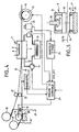
- This comprises a press 7 comprising two plates or possibly two rollers 8 and 9 juxtaposed between which circulate patterned bands 10 and 11 to be assembled by gluing.
- the plate or the upper roller 8 is heated to a bonding temperature of approximately 200 ° C. by an electrical resistance R supplied by a device for supplying external electrical current, not shown.
- the lower plate 9 is cooled by a water circulation circuit 12 passing through a heat exchanger 13 of the heat pump type, or any other equivalent device actuated by a pump 14.
- the strips 10 and 11, once bonded, are entrained in a translational movement between the two plates or rollers 8 and 9 by a pin wheel 15 whose teeth mesh in the perforations 6 of the support strip or clamp system with transverse movement.
- the spike wheel 15 is driven by a motor 16.
- the strips 10 and 11 are unwound respectively from two loading rollers 17 and 18. In fact in order to obtain a continuous assembly of the strips 10 and 11 these are each mounted on an unwinder and driven by a motor not shown.
- the strip 10 is mounted on the roller 17, while the strip 11 is mounted on the roller 18.
- the strip 10 is wound on itself with an intermediate strip 41 which falls as the strip 10. unfolds. intermediate strip 41 makes it possible to prevent the patterns from overlapping one another.
- the strip 11 is also wound on itself.
- An intermediate strip 51 can also be provided to avoid any discomfort during the unwinding of the strip 11.
- the traction of the support strip 10 is adjusted by a pressing wheel 19 on a beam 20 of the support strip 10.
- the beam 20 then retains the strip 10 by friction and provides the tension of this strip.
- the tension of the strip to be bonded 11 is adjusted by two pressure rollers 21 and 22 with calibrated friction.
- a control member 23 provides, on the one hand, the rotation control of the motor 16 and of the pump 14 and, on the other hand, that of the press wheel 19.
- the controller 23 receives information from, on the one hand, a camera 24 via an image analyzer 25, on the other hand, a temperature sensor 26 connected to the circuit of circulation of fluid 12, as well as of a device 27 formed by a tensiometer or any other equivalent device for measuring the tension of the support strip 10.
- the image analyzer 25 can permanently provide information on the delta X and delta Y offset of the reference hole or of indexing relative to the reference axes X and Y of each pattern.
- the advantage of this arrangement is that it makes it possible, thanks to the control member 23, to act jointly or in isolation on the pressure exerted on the strip 10 or the strip 11 respectively, by the press wheel 19 to adjust the tension.
- the compensation for this offset is effected by the control member 23 by acting on the cooling of the plate 9, in the other case the compensation is effected by acting on the pressure rollers 19 or 21, 22.
- the strip which has the highest coefficient of expansion on the plate or roller 9 which is cooled the other strip 11 being applied against the plate or roller 8 which is heated.
- Kapton for bonding a copper roll which has a coefficient of expansion of 17.10 -6 / ° C on a roll of a plastic material marketed under the registered trademark "Kapton" which has a coefficient of expansion of 20.10 -6 / ° C, the Kapton must be applied to the plate or roller 9 and the copper to the plate or pressure roller 8.
- the squab press solution including a diagram of embodiment is shown in Figure 5 has the advantage to be simple to carry out and to offer pressure homogeneous between the two plates.
- a press with pigeon has a lower plate 9 formed by a steel plate 28 mounted on an insulating plate 29 and an upper plate 8 formed by a steel plate 30 comprising a hollow insulating cap 31 containing the head 32 of a youngster 33.
- the steel plate 28 has on the surface facing the plate in steel 30 distribution springs 34 which allow the squab head 32, the steel plate 30 and the spring 34 to be in contact all together before the pressure of the two plates 28 and 30 is exerted on the two bands 10 and 11, which prevents any movement in the X and Y directions when tightening the two plates.
- the collage can still be homogenized by possibly a second press not shown which then has the same temperatures on the two trays or by two rollers similar to those already used in the state of the art.
- the process according to the invention allows the manufacture of integrated circuit micromodules, this manufacturing including banding metallic precut including including regular perforations allowing training of the band by toothed wheel (in the manner of training of a cinema film), the formation of a band very thin perforated dielectric, then bonding of two strips against each other, sticking a chip integrated circuit against the thin dielectric strip, and the formation of electrical connections between the chip and the metal strip across the cutouts of the dielectric strip.
- the dielectric strip will be narrower than the metal strip, it will not will not include periodic side cuts allowing a drive by cogwheels, and it will generally be too thin to allow a gear drive.
- the cuts allowing the training of the band metal will not be covered by the tape dielectric thanks to the lower width thereof.
- Other manufacturing operations can be conventional, for example: depositing a drop of resin to coat the chip and bonding connections with the chip, on the side of the dielectric strip but not on the side of the metal strip; and possibly leveling gout at a predetermined height; separation of micromodule with the rest of the strip; the micromodule is then ready to be inserted into a card cavity plastic.
- the chip can be glued on the strip dielectric or on the metal strip.
- the cases in which it is not necessary to provide a contact rear panel for the chip are indeed common in CMOS technology.
- the thin dielectric placed under the card acts as an elastic buffer which in some cases it prevents the chip from getting deteriorated.
- the small thickness of the dielectric strip facilitates very effective bonding of two strips against each other, without risk of detachment during subsequent processing.
- Another advantage of the invention is that the sticking the chip on the dielectric allows to predict a single micromodule production line whatever either the dimension of the chip to be encapsulated, and this from a single model of precut metal strip, on the sole condition of providing a cutting tool changeable or removable for cutting out in the dielectric strip; indeed, the chip is isolated of the metal grid, and only the location of the perforations in the dielectric defines the position connections between the chip and the grid; for a chip larger, we will place the perforations more distant from the center of the chip; for a more chip small, we will bring the perforations closer to the center; he It is of course sufficient that the perforations remain at the above suitable metal ranges, but these ranges can be quite wide in the case of micromodules with low number of external contacts (6 or 8 for example).
Landscapes
- Engineering & Computer Science (AREA)
- Computer Hardware Design (AREA)
- Microelectronics & Electronic Packaging (AREA)
- Physics & Mathematics (AREA)
- General Physics & Mathematics (AREA)
- Theoretical Computer Science (AREA)
- Condensed Matter Physics & Semiconductors (AREA)
- Power Engineering (AREA)
- Computer Networks & Wireless Communication (AREA)
- Manufacturing & Machinery (AREA)
- Credit Cards Or The Like (AREA)
- Wire Bonding (AREA)
- Shaping Of Tube Ends By Bending Or Straightening (AREA)
- Laminated Bodies (AREA)
Abstract
Description
D'autre part il est impératif de réaliser une perforation dans chaque feuille d'isolant à l'emplacement réservé pour le circuit afin d'y loger le circuit et de rentrer ainsi dans les tolérances exigées sur l'épaisseur pour la fabrication des cartes à puce.
- la figure 1, une vue de dessus d'une bande métallique prédécoupée selon l'invention,
- la figure 2, une vue de dessus d'une bande diélectrique perforée selon l'invention, destinée à être collée sur la bande métallique de la figure 1,
- la figure 3, une vue montrant la juxtaposition des deux bandes en cours de collage,
- la figure 4, un dispositif pour la mise en oeuvre du procédé selon l'invention,
- la figure 5, une représentation d'une presse à pigeonneau utilisée pour la mise en oeuvre du procédé selon l'invention.
La bande 10 est montée sur le rouleau 17, alors que la bande 11 est montée sur le rouleau 18. La bande 10 est enroulée sur elle même avec une bande intercalaire 41 qui tombe au fur et à mesure du déroulement de la bande 10. Cette bande intercalaire 41 permet d'éviter que les motifs ne s'imbriquent les uns dans les autres. La bande 11 est également enroulée sur elle même. Une bande intercalaire 51 peut être prévue aussi pour éviter toute gène lors du déroulement de la bande 11.
La traction de la bande support 10 est réglée par une roue presseuse 19 sur une poutre 20 de la bande support 10. La poutre 20 retient alors la bande 10 par frottement et procure la tension de cette bande. La tension de la bande à coller 11 est réglée par deux rouleaux presseurs 21 et 22 à frottement calibré. Un organe de commande 23 assure d'une part, la commande en rotation du moteur 16 et de la pompe 14 et d'autre part, celle de la roue presseuse 19.
L'organe de commande 23 reçoit des informations provenant d'une part, d'une caméra 24 par l'intermédiaire d'un analyseur d'image 25, d'autre part, d'un capteur de température 26 branché sur le circuit de circulation de fluide 12, ainsi que d'un dispositif 27 formé par un tensiomètre ou tout autre dispositif équivalent pour mesurer la tension de la bande support 10. Ainsi, lorsque les deux bandes 10 et 11 entraínées par la traction du moteur 16 défilent sous les rouleaux ou entre les deux plateaux 8 et 9 l'analyseur d'image 25 peut fournir en permanence des informations de décalage delta X et delta Y du trou repère ou d'indexation relativement aux axes repères X et Y de chaque motif. L'intérêt de cette disposition est qu'elle permet, grâce à l'organe de commande 23, d'agir conjointement ou isolément sur la pression exercée sur la bande 10 ou la bande 11 respectivement, par la roue presseuse 19 pour régler la tension de la bande 10 ou de la bande 11 par les rouleaux presseurs 21 et 22 et par réglage des températures des deux plateaux ou rouleaux presseurs 8 et 9 afin d'ajuster, par extension ou dilatation la position d'une bande par rapport à l'autre pour faire coïncider les pas des motifs des deux bandes en annulant les décalages delta X et delta Y du trou repère par rapport aux axes repères X et Y. Il faut noter cependant qu'un réglage du pas par simple extension d'une des deux bandes l'une par rapport à l'autre ne vaut que pour des faibles décalages delta X et/ou delta Y des valeurs du pas, que les grands décalages ne peuvent être compensés efficacement que par un ajustement des températures relatives des plateaux ou rouleaux 8 et 9 l'une par rapport à l'autre. En pratique, lorsqu'un décalage delta X a dépassé un seuil prédéterminé, la compensation de ce décalage est effectuée par l'organe de commande 23 en agissant sur le refroidissement du plateau 9, dans l'autre cas la compensation s'effectue en agissant sur les rouleaux presseurs 19 ou 21, 22. Cependant, pour que le système fonctionne efficacement il est préférable d'appliquer la bande qui a le coefficient de dilatation le plus important sur le plateau ou rouleau 9 qui est refroidi, l'autre bande 11 étant appliquée contre le plateau ou rouleau 8 qui est chauffé. Ainsi, par exemple, pour un collage d'un rouleau de cuivre qui a un coefficient de dilatation de 17.10-6/°C sur un rouleau d'une matière plastique commercialisée sous la marque déposée "Kapton" qui a un coefficient de dilatation de 20.10-6/°C, le Kapton doit être appliqué sur le plateau ou rouleau 9 et le cuivre sur le plateau ou rouleau presseur 8.
Claims (15)
- Procédé d'assemblage en continu de bandes à motifs (10, 11) dont l'une est une bande métallique prédécoupée et l'autre une bande d'isolant perforée, ces bandes comportant des repères (I) de pas de motifs et étant dévidées à partir de deux rouleaux de chargement, ce procédé consistant à coller par pression à chaud la première bande (11) sur la deuxième bande (10) au travers d'une presse à coller (8, 9) et à juxtaposer, au moment du collage, les repères de pas de motifs de chaque bande, ce procédé comportant les étapes consistant à repérer sur chacune des bandes les repères de pas de motifs, et ensuite à ajuster les deux bandes l'une par rapport à l'autre par extension d'au moins une bande par rapport à l'autre et/ou par un échauffement différent de chacune des bandes en regard, ce qui provoque un déplacement relatif des deux bandes l'une par rapport à l'autre par dilatation et permet ainsi de juxtaposer les repères de pas de motifs de chaque bande.
- Procédé selon la revendication 1, dans lequel une presse (7) à plateau est utilisée, comportant un premier plateau (8) chauffé électriquement et un deuxième plateau (9) refroidi par circulation d'un fluide.
- Procédé selon la revendication 2, dans lequel un organe de commande (23) pour régler les températures des deux plateaux (8, 9) et les tensions des deux bandes (10, 11) est mis en oeuvre.
- Procédé selon la revendication 2, dans lequel la presse (7) est une presse à pigeonneau (33).
- Procédé selon l'une quelconque des revendications 1 à 4, dans lequel la position relative des repères des pas des motifs est repérée par une caméra de télévision (24) couplée à un organe de commande (23) par l'intermédiaire d'un analyseur d'image (25).
- Procédé selon l'une quelconque des revendications 1 à 5, dans lequel la première bande à motifs (10) est en cuivre et la deuxième bande à motifs (11) est en Kapton.
- Procédé selon l'une quelconque des revendications 2 à 4, et 5 et 6 lorsque que celles-ci dépendent de la revendication 2, dans lequel la bande à motifs (10) qui a le coefficient de dilatation le plus élevé est appliquée sur le deuxième plateau (9) refroidi par circulation d'un fluide.
- Procédé selon l'une quelconque des revendications précédentes, dans lequel les pas de motifs des bandes (10, 11) sont identiques ou sont des multiples.
- Dispositif d'assemblage en continu par collage par pression à chaud au travers d'une presse à coller de bandes à motifs (10, 11) dont l'une est une bande métallique prédécoupée et l'autre est une bande d'isolant préperforée, ces bandes comportant des repères (I) de pas de motifs, le dispositif comportant des moyens de chargement des bandes comprenant un premier dérouleur de bandes (17) sur lequel est montée la bande métallique (10) enroulée sur elle-même avec une bande intercalaire (41) empêchant l'imbrication des motifs, un deuxième dérouleur de bande (18) sur lequel est montée la bande d'isolant (11), ladite bande étant enroulée sur elle-même, le dispositif comportant en outre des moyens de repérage (23, 24, 25) des repères de pas de motifs de chaque bande, des moyens de réglage de la tension (19, 21, 22, 23) de l'une ou de l'autre bande et des moyens d'ajustage (8, 9) de cette tension aptes à provoquer un échauffement différent de chacune des bandes en regard, de manière à réaliser un déplacement relatif des deux bandes l'une par rapport à l'autre par dilatation et à juxtaposer les repères de pas de motifs de chaque bande.
- Dispositif selon la revendication 9, dans lequel la presse à coller est une presse (7) à plateau comprenant un premier plateau (8) chauffé électriquement et un deuxième plateau (9) refroidi par circulation d'un fluide.
- Dispositif selon la revendication 10, comprenant en outre des moyens de commande (23) pour régler les températures des deux plateaux (8, 9).
- Dispositif selon la revendication 11, dans lequel les moyens de commande (23) permettent de régler les tensions des deux bandes.
- Dispositif selon la revendication 10, dans lequel la presse (7) est une presse à pigeonneau (33).
- Dispositif selon la revendication 9, dans lequel les moyens de repérage comprennent une caméra de télévision (24) couplée à un organe de commande (23) par l'intermédiaire d'un analyseur d'image (25).
- Dispositif selon l'une quelconque des revendications 9 à 14, dans lequel la première bande à motifs (10) est en cuivre et la deuxième bande à motifs est en Kapton.
Priority Applications (1)
| Application Number | Priority Date | Filing Date | Title |
|---|---|---|---|
| EP96106073A EP0734063A3 (fr) | 1991-02-19 | 1992-02-18 | Micromodule de circuit intégré obtenu par un procédé d'assemblage en continu de bandes à motifs |
Applications Claiming Priority (3)
| Application Number | Priority Date | Filing Date | Title |
|---|---|---|---|
| FR9101934A FR2673041A1 (fr) | 1991-02-19 | 1991-02-19 | Procede de fabrication de micromodules de circuit integre et micromodule correspondant. |
| FR9101934 | 1991-02-19 | ||
| PCT/FR1992/000158 WO1992015118A1 (fr) | 1991-02-19 | 1992-02-18 | Procede d'assemblage en continu de bandes a motifs et micromodule de circuit integre obtenu par ledit procede |
Related Child Applications (2)
| Application Number | Title | Priority Date | Filing Date |
|---|---|---|---|
| EP96106073A Division EP0734063A3 (fr) | 1991-02-19 | 1992-02-18 | Micromodule de circuit intégré obtenu par un procédé d'assemblage en continu de bandes à motifs |
| EP96106073.8 Division-Into | 1996-04-18 |
Publications (2)
| Publication Number | Publication Date |
|---|---|
| EP0572514A1 EP0572514A1 (fr) | 1993-12-08 |
| EP0572514B1 true EP0572514B1 (fr) | 1999-05-12 |
Family
ID=9409853
Family Applications (2)
| Application Number | Title | Priority Date | Filing Date |
|---|---|---|---|
| EP96106073A Ceased EP0734063A3 (fr) | 1991-02-19 | 1992-02-18 | Micromodule de circuit intégré obtenu par un procédé d'assemblage en continu de bandes à motifs |
| EP92906568A Expired - Lifetime EP0572514B1 (fr) | 1991-02-19 | 1992-02-18 | Procédé et dispositif d'assemblage en continu de bandes à motifs |
Family Applications Before (1)
| Application Number | Title | Priority Date | Filing Date |
|---|---|---|---|
| EP96106073A Ceased EP0734063A3 (fr) | 1991-02-19 | 1992-02-18 | Micromodule de circuit intégré obtenu par un procédé d'assemblage en continu de bandes à motifs |
Country Status (8)
| Country | Link |
|---|---|
| US (2) | US5470411A (fr) |
| EP (2) | EP0734063A3 (fr) |
| JP (2) | JP2700172B2 (fr) |
| CA (1) | CA2104374C (fr) |
| DE (1) | DE69229168T2 (fr) |
| ES (1) | ES2133318T3 (fr) |
| FR (1) | FR2673041A1 (fr) |
| WO (1) | WO1992015118A1 (fr) |
Families Citing this family (117)
| Publication number | Priority date | Publication date | Assignee | Title |
|---|---|---|---|---|
| DE4224103A1 (de) * | 1992-07-22 | 1994-01-27 | Manfred Dr Ing Michalk | Miniaturgehäuse mit elektronischen Bauelementen |
| US7158031B2 (en) | 1992-08-12 | 2007-01-02 | Micron Technology, Inc. | Thin, flexible, RFID label and system for use |
| DE59406668D1 (de) * | 1993-12-02 | 1998-09-17 | Heraeus Gmbh W C | Verfahren und Vorrichtung zur Herstellung eines Folienverbundes |
| DE4340996C1 (de) * | 1993-12-02 | 1995-03-02 | Heraeus Gmbh W C | Verfahren und Vorrichtung zur Herstellung eines Folienverbundes |
| FR2724477B1 (fr) | 1994-09-13 | 1997-01-10 | Gemplus Card Int | Procede de fabrication de cartes sans contact |
| DE4437721A1 (de) * | 1994-10-21 | 1996-04-25 | Giesecke & Devrient Gmbh | Kontaktloses elektronisches Modul |
| DE4442920C2 (de) | 1994-12-02 | 2001-02-22 | Heraeus Gmbh W C | Verfahren zur Herstellung eines Folienverbundes |
| US5558687A (en) * | 1994-12-30 | 1996-09-24 | Corning Incorporated | Vertical, packed-bed, film evaporator for halide-free, silicon-containing compounds |
| FR2733553B1 (fr) * | 1995-04-25 | 1997-07-11 | Pem Sa Protection Electrolytiq | Dispositif de contre-collage pour la solidarisation d'une bande metallique et d'une bande de materiau isolant |
| FR2734983B1 (fr) * | 1995-05-29 | 1997-07-04 | Sgs Thomson Microelectronics | Utilisation d'un micromodule comme boitier de montage en surface et procede correspondant |
| DE19521022C2 (de) * | 1995-06-13 | 1997-04-10 | Heraeus Gmbh W C | Verfahren zur Herstellung eines Schichtverbundes |
| FR2741191B1 (fr) * | 1995-11-14 | 1998-01-09 | Sgs Thomson Microelectronics | Procede de fabrication d'un micromodule, notamment pour cartes a puces |
| DE19543427C2 (de) * | 1995-11-21 | 2003-01-30 | Infineon Technologies Ag | Chipmodul, insbesondere zum Einbau in eine Chipkarte |
| US5766389A (en) * | 1995-12-29 | 1998-06-16 | Kimberly-Clark Worldwide, Inc. | Disposable absorbent article having a registered graphic and process for making |
| US5818719A (en) * | 1995-12-29 | 1998-10-06 | Kimberly-Clark, Worldwide, Inc. | Apparatus for controlling the registration of two continuously moving layers of material |
| DE19632795A1 (de) * | 1996-08-15 | 1998-02-19 | Cicorel S A | Verfahren und Vorrichtung zum Laminieren von Folienbahnen |
| JP2786620B2 (ja) * | 1996-08-23 | 1998-08-13 | 三菱重工業株式会社 | 段ボールシートの製造装置 |
| JP3520186B2 (ja) * | 1996-09-30 | 2004-04-19 | 東芝マイクロエレクトロニクス株式会社 | フィルムキャリアテープの製造方法、フィルムキャリアテープの製造装置 |
| US6033502A (en) | 1996-11-13 | 2000-03-07 | Kimberly-Clark Worldwide, Inc. | Process and apparatus for registering continuously moving stretchable layers |
| US5930139A (en) * | 1996-11-13 | 1999-07-27 | Kimberly-Clark Worldwide, Inc. | Process and apparatus for registration control of material printed at machine product length |
| US5964970A (en) * | 1997-10-14 | 1999-10-12 | Kimberly-Clark Worldwide, Inc. | Registration process and apparatus for continuously moving elasticized layers having multiple components |
| US6092002A (en) * | 1996-11-13 | 2000-07-18 | Kimberly-Clark Worldwide, Inc. | Variable tension process and apparatus for continuously moving layers |
| US5932039A (en) * | 1997-10-14 | 1999-08-03 | Kimberly-Clark Wordwide, Inc. | Process and apparatus for registering a continuously moving, treatable layer with another |
| JP3389053B2 (ja) | 1997-05-07 | 2003-03-24 | 三菱重工業株式会社 | 複数層の芯紙を有する段ボールシートの位相制御方法 |
| US6980085B1 (en) * | 1997-08-18 | 2005-12-27 | Micron Technology, Inc. | Wireless communication devices and methods of forming and operating the same |
| US6339385B1 (en) | 1997-08-20 | 2002-01-15 | Micron Technology, Inc. | Electronic communication devices, methods of forming electrical communication devices, and communication methods |
| DE19739042A1 (de) | 1997-09-05 | 1999-03-11 | Kannegiesser H Gmbh Co | Verfahren und Vorrichtung zum Verbinden flexibler Flächengebilde |
| US6002169A (en) * | 1998-06-15 | 1999-12-14 | Lsi Logic Corporation | Thermally enhanced tape ball grid array package |
| FR2780848A1 (fr) * | 1998-07-06 | 2000-01-07 | Solaic Sa | Antenne a bornes de connexion ajourees pour carte a circuit integre, et carte a circuit integre comprenant une telle antenne |
| FR2781973B1 (fr) * | 1998-07-29 | 2006-07-07 | Solaic Sa | Feuille d'antennes comportant des reperes, plaque contenant plusieurs emplacements de corps de carte et incluant une telle feuille d'antennes, et procede de decoupe de cette plaque |
| US6428641B1 (en) * | 1998-08-31 | 2002-08-06 | Amkor Technology, Inc. | Method for laminating circuit pattern tape on semiconductor wafer |
| US6479887B1 (en) | 1998-08-31 | 2002-11-12 | Amkor Technology, Inc. | Circuit pattern tape for wafer-scale production of chip size semiconductor packages |
| US6652686B1 (en) | 1999-02-08 | 2003-11-25 | Kimberly-Clark Worldwide, Inc. | Processes and apparatus for making disposable absorbent articles |
| DE19920593B4 (de) * | 1999-05-05 | 2006-07-13 | Assa Abloy Identification Technology Group Ab | Chipträger für ein Chipmodul und Verfahren zur Herstellung des Chipmoduls |
| FR2796203B1 (fr) * | 1999-07-08 | 2001-08-31 | Gemplus Card Int | Module electronique sans contact et procede pour son obtention |
| FR2798002B1 (fr) * | 1999-08-26 | 2001-11-02 | Gemplus Card Int | Procede de fabrication de micromodules electroniques comprenant une antenne et micromodules obtenus par le procede |
| JP4012733B2 (ja) * | 1999-09-20 | 2007-11-21 | フラクトゥス・ソシエダッド・アノニマ | マルチレベルアンテナ |
| JP3644859B2 (ja) * | 1999-12-02 | 2005-05-11 | 沖電気工業株式会社 | 半導体装置 |
| EP1592083B1 (fr) | 2000-01-19 | 2013-04-03 | Fractus, S.A. | antennes miniatures de remplissage d'espace |
| US6986820B2 (en) * | 2000-01-21 | 2006-01-17 | Kimberly-Clark Worldwide, Inc. | Processes and apparatus for making disposable absorbent articles |
| US6714136B1 (en) * | 2000-08-14 | 2004-03-30 | Computime, Ltd. | Alarm clock with remote control function |
| EP1310004A2 (fr) * | 2000-08-18 | 2003-05-14 | Siemens Aktiengesellschaft | Transistor a effet de champ organique (ofet), procede de fabrication et circuit integre comportant celui-ci, et leurs utilisations |
| US7875975B2 (en) * | 2000-08-18 | 2011-01-25 | Polyic Gmbh & Co. Kg | Organic integrated circuit completely encapsulated by multi-layered barrier and included in RFID tag |
| DE10044842A1 (de) * | 2000-09-11 | 2002-04-04 | Siemens Ag | Organischer Gleichrichter, Schaltung, RFID-Tag und Verwendung eines organischen Gleichrichters |
| EP1323195A1 (fr) * | 2000-09-22 | 2003-07-02 | Siemens Aktiengesellschaft | Electrode et trace conducteur pour composants organiques et procede de production correspondant |
| DE10116510A1 (de) * | 2000-11-27 | 2002-05-29 | Orient Semiconductor Elect Ltd | Ultradünnfilm-Kapselung |
| DE10061286C1 (de) * | 2000-12-08 | 2002-04-04 | Hollingsworth Gmbh | Vorrichtung zum Aufziehen einer Kardiergarnitur |
| DE10061297C2 (de) | 2000-12-08 | 2003-05-28 | Siemens Ag | Verfahren zur Sturkturierung eines OFETs |
| DE10061299A1 (de) * | 2000-12-08 | 2002-06-27 | Siemens Ag | Vorrichtung zur Feststellung und/oder Weiterleitung zumindest eines Umwelteinflusses, Herstellungsverfahren und Verwendung dazu |
| DE10105914C1 (de) * | 2001-02-09 | 2002-10-10 | Siemens Ag | Organischer Feldeffekt-Transistor mit fotostrukturiertem Gate-Dielektrikum und ein Verfahren zu dessen Erzeugung |
| US6582887B2 (en) * | 2001-03-26 | 2003-06-24 | Daniel Luch | Electrically conductive patterns, antennas and methods of manufacture |
| US7394425B2 (en) * | 2001-03-26 | 2008-07-01 | Daniel Luch | Electrically conductive patterns, antennas and methods of manufacture |
| US7452656B2 (en) | 2001-03-26 | 2008-11-18 | Ertek Inc. | Electrically conductive patterns, antennas and methods of manufacture |
| WO2002078052A2 (fr) * | 2001-03-26 | 2002-10-03 | Siemens Aktiengesellschaft | Appareil comprenant au moins deux composants electroniques organiques et son procede de production |
| US7564409B2 (en) * | 2001-03-26 | 2009-07-21 | Ertek Inc. | Antennas and electrical connections of electrical devices |
| GB0108655D0 (en) * | 2001-04-06 | 2001-05-30 | Koninkl Philips Electronics Nv | Microwave circuit |
| DE10120269C1 (de) * | 2001-04-25 | 2002-07-25 | Muehlbauer Ag | Verfahren zum Verbinden von Mikrochips mit auf einem Trägerband angeordneten Antennen zum Herstellen eines Transponders |
| DE10126860C2 (de) * | 2001-06-01 | 2003-05-28 | Siemens Ag | Organischer Feldeffekt-Transistor, Verfahren zu seiner Herstellung und Verwendung zum Aufbau integrierter Schaltungen |
| DE10126859A1 (de) * | 2001-06-01 | 2002-12-12 | Siemens Ag | Verfahren zur Erzeugung von leitfähigen Strukturen mittels Drucktechnik sowie daraus hergestellte aktive Bauelemente für integrierte Schaltungen |
| JP4663172B2 (ja) * | 2001-07-31 | 2011-03-30 | 三洋電機株式会社 | 半導体装置の製造方法 |
| RU2300159C2 (ru) | 2001-09-18 | 2007-05-27 | Награид Са | Способ изготовления карт или электронных этикеток |
| DE10151036A1 (de) | 2001-10-16 | 2003-05-08 | Siemens Ag | Isolator für ein organisches Elektronikbauteil |
| DE10151440C1 (de) * | 2001-10-18 | 2003-02-06 | Siemens Ag | Organisches Elektronikbauteil, Verfahren zu seiner Herstellung und seine Verwendung |
| JP3978019B2 (ja) * | 2001-11-19 | 2007-09-19 | 矢崎化工株式会社 | 樹脂被覆鋼管における鋼管と被覆樹脂の分離回収方法、及び分離回収設備 |
| DE10160732A1 (de) * | 2001-12-11 | 2003-06-26 | Siemens Ag | Organischer Feld-Effekt-Transistor mit verschobener Schwellwertspannung und Verwendung dazu |
| DE10212640B4 (de) * | 2002-03-21 | 2004-02-05 | Siemens Ag | Logische Bauteile aus organischen Feldeffekttransistoren |
| DE10212639A1 (de) * | 2002-03-21 | 2003-10-16 | Siemens Ag | Vorrichtung und Verfahren zur Laserstrukturierung von Funktionspolymeren und Verwendungen |
| DE10226370B4 (de) * | 2002-06-13 | 2008-12-11 | Polyic Gmbh & Co. Kg | Substrat für ein elektronisches Bauteil, Verwendung des Substrates, Verfahren zur Erhöhung der Ladungsträgermobilität und Organischer Feld-Effekt Transistor (OFET) |
| US8044517B2 (en) * | 2002-07-29 | 2011-10-25 | Polyic Gmbh & Co. Kg | Electronic component comprising predominantly organic functional materials and a method for the production thereof |
| DE10237084A1 (de) * | 2002-08-05 | 2004-02-19 | Osram Opto Semiconductors Gmbh | Verfahren zum Herstellen eines elektrischen Leiterrahmens und Verfahren zum Herstellen eines oberflächenmontierbaren Halbleiterbauelements |
| EP1526902B1 (fr) * | 2002-08-08 | 2008-05-21 | PolyIC GmbH & Co. KG | Appareil electronique |
| ATE355566T1 (de) | 2002-08-23 | 2006-03-15 | Polyic Gmbh & Co Kg | Organisches bauelement zum überspannungsschutz und dazugehörige schaltung |
| EP1559148A2 (fr) * | 2002-11-05 | 2005-08-03 | Siemens Aktiengesellschaft | Composant electronique organique a structuration haute resolution et procede de production de ce composant |
| EP1563570A1 (fr) | 2002-11-07 | 2005-08-17 | Fractus, S.A. | Boitier de circuit integre incluant une antenne miniature |
| DE10253154A1 (de) * | 2002-11-14 | 2004-05-27 | Siemens Ag | Messgerät zur Bestimmung eines Analyten in einer Flüssigkeitsprobe |
| GB2395481B (en) * | 2002-11-19 | 2006-06-28 | C Tech Innovation Ltd | Control of biocatalysis reactions |
| US7442954B2 (en) * | 2002-11-19 | 2008-10-28 | Polyic Gmbh & Co. Kg | Organic electronic component comprising a patterned, semi-conducting functional layer and a method for producing said component |
| EP1563554B1 (fr) * | 2002-11-19 | 2012-01-04 | PolyIC GmbH & Co. KG | Composant electronique organique comportant le meme materiau organique pour au moins deux couches fonctionnelles |
| DE10300521A1 (de) * | 2003-01-09 | 2004-07-22 | Siemens Ag | Organoresistiver Speicher |
| DE112004000012B4 (de) * | 2003-01-21 | 2012-06-14 | Polyic Gmbh & Co. Kg | Kunststoffprodukt mit integriertem organischen elektronischen Bauteil, Verfahren zur Herstellung dazu |
| DE10302149A1 (de) * | 2003-01-21 | 2005-08-25 | Siemens Ag | Verwendung leitfähiger Carbon-black/Graphit-Mischungen für die Herstellung von low-cost Elektronik |
| EP1586127B1 (fr) * | 2003-01-21 | 2007-05-02 | PolyIC GmbH & Co. KG | Composant electronique organique et procede de fabrication de dispositifs electroniques organiques |
| DE10318688A1 (de) * | 2003-04-24 | 2004-11-25 | W. C. Heraeus Gmbh & Co. Kg | Verfahren zum Trennen der elektrischen Verbindungsknoten bei IC-Frames und Verfahren zur Herstellung eines elektronischen Bauteils sowie von Frames dafür |
| DE10330064B3 (de) * | 2003-07-03 | 2004-12-09 | Siemens Ag | Logikgatter mit potentialfreier Gate-Elektrode für organische integrierte Schaltungen |
| DE10330062A1 (de) * | 2003-07-03 | 2005-01-27 | Siemens Ag | Verfahren und Vorrichtung zur Strukturierung von organischen Schichten |
| DE10338277A1 (de) * | 2003-08-20 | 2005-03-17 | Siemens Ag | Organischer Kondensator mit spannungsgesteuerter Kapazität |
| DE10339036A1 (de) | 2003-08-25 | 2005-03-31 | Siemens Ag | Organisches elektronisches Bauteil mit hochaufgelöster Strukturierung und Herstellungsverfahren dazu |
| DE10340643B4 (de) * | 2003-09-03 | 2009-04-16 | Polyic Gmbh & Co. Kg | Druckverfahren zur Herstellung einer Doppelschicht für Polymerelektronik-Schaltungen, sowie dadurch hergestelltes elektronisches Bauelement mit Doppelschicht |
| DE10340644B4 (de) * | 2003-09-03 | 2010-10-07 | Polyic Gmbh & Co. Kg | Mechanische Steuerelemente für organische Polymerelektronik |
| GB0328246D0 (en) * | 2003-12-04 | 2004-06-16 | Qinetiq Ltd | Improvements relating to electronic circuit packages |
| US7397067B2 (en) * | 2003-12-31 | 2008-07-08 | Intel Corporation | Microdisplay packaging system |
| DE102004002024A1 (de) * | 2004-01-14 | 2005-08-11 | Siemens Ag | Organischer Transistor mit selbstjustierender Gate-Elektrode und Verfahren zu dessen Herstellung |
| DE102004025911B4 (de) * | 2004-05-27 | 2008-07-31 | Infineon Technologies Ag | Kontaktbehaftete Chipkarte, Verfahren zur Herstellung einer solchen |
| US8330259B2 (en) | 2004-07-23 | 2012-12-11 | Fractus, S.A. | Antenna in package with reduced electromagnetic interaction with on chip elements |
| US9053401B2 (en) * | 2004-07-30 | 2015-06-09 | Semiconductor Energy Laboratory Co., Ltd. | Laminating system, IC sheet, scroll of IC sheet, and method for manufacturing IC chip |
| US20150287660A1 (en) | 2007-01-05 | 2015-10-08 | Semiconductor Energy Laboratory Co., Ltd. | Laminating system, ic sheet, scroll of ic sheet, and method for manufacturing ic chip |
| DE102004040831A1 (de) * | 2004-08-23 | 2006-03-09 | Polyic Gmbh & Co. Kg | Funketikettfähige Umverpackung |
| DE102004059465A1 (de) * | 2004-12-10 | 2006-06-14 | Polyic Gmbh & Co. Kg | Erkennungssystem |
| DE102004059464A1 (de) * | 2004-12-10 | 2006-06-29 | Polyic Gmbh & Co. Kg | Elektronikbauteil mit Modulator |
| DE102004059467A1 (de) * | 2004-12-10 | 2006-07-20 | Polyic Gmbh & Co. Kg | Gatter aus organischen Feldeffekttransistoren |
| DE102004063435A1 (de) | 2004-12-23 | 2006-07-27 | Polyic Gmbh & Co. Kg | Organischer Gleichrichter |
| DE102005009819A1 (de) | 2005-03-01 | 2006-09-07 | Polyic Gmbh & Co. Kg | Elektronikbaugruppe |
| DE102005009820A1 (de) * | 2005-03-01 | 2006-09-07 | Polyic Gmbh & Co. Kg | Elektronikbaugruppe mit organischen Logik-Schaltelementen |
| DE102005017655B4 (de) | 2005-04-15 | 2008-12-11 | Polyic Gmbh & Co. Kg | Mehrschichtiger Verbundkörper mit elektronischer Funktion |
| DE102005031448A1 (de) | 2005-07-04 | 2007-01-11 | Polyic Gmbh & Co. Kg | Aktivierbare optische Schicht |
| DE102005035589A1 (de) | 2005-07-29 | 2007-02-01 | Polyic Gmbh & Co. Kg | Verfahren zur Herstellung eines elektronischen Bauelements |
| DE102005044306A1 (de) | 2005-09-16 | 2007-03-22 | Polyic Gmbh & Co. Kg | Elektronische Schaltung und Verfahren zur Herstellung einer solchen |
| EP1785916B1 (fr) * | 2005-11-14 | 2009-08-19 | Tyco Electronics France SAS | Corps de carte à puce, carte à puce et procédé de fabrication |
| US8196829B2 (en) * | 2006-06-23 | 2012-06-12 | Fractus, S.A. | Chip module, sim card, wireless device and wireless communication method |
| US8738103B2 (en) * | 2006-07-18 | 2014-05-27 | Fractus, S.A. | Multiple-body-configuration multimedia and smartphone multifunction wireless devices |
| JP2006344994A (ja) * | 2006-08-28 | 2006-12-21 | Oki Electric Ind Co Ltd | 半導体装置の製造方法 |
| EP2008813A1 (fr) * | 2007-06-29 | 2008-12-31 | Nederlandse Organisatie voor toegepast- natuurwetenschappelijk onderzoek TNO | Dispositif de laminage, procédé de laminage et feuille. |
| JP4702392B2 (ja) * | 2008-04-28 | 2011-06-15 | カシオ計算機株式会社 | 共鳴音発生装置および電子楽器 |
| KR101035054B1 (ko) * | 2008-12-24 | 2011-05-19 | 전자부품연구원 | 태그 안테나 및 그 제조방법 |
| DE102011010984B4 (de) | 2011-02-10 | 2012-12-27 | Heraeus Materials Technology Gmbh & Co. Kg | Verfahren zum partiellen Laminieren von flexiblen Substraten |
| RU2508991C1 (ru) | 2012-12-28 | 2014-03-10 | Олег Умарович Айбазов | Бесконтактная чип-карта |
| IT201700035537A1 (it) * | 2017-03-31 | 2018-10-01 | Fillshape Srl | Procedimento ed apparato per la fabbricazione di buste per contenitori alimentari di tipo doypack e simili. |
Family Cites Families (29)
| Publication number | Priority date | Publication date | Assignee | Title |
|---|---|---|---|---|
| US3458382A (en) * | 1965-10-24 | 1969-07-29 | Schjeldahl Co G T | Laminator assembly |
| CH608314A5 (en) * | 1976-04-02 | 1978-12-29 | Ret Sa Rech Economiques Et Tec | Process for manufacturing a tape support for mounting integrated electronic components, and tape support obtained by this process |
| US4295912A (en) * | 1978-07-03 | 1981-10-20 | National Semiconductor Corporation | Apparatus and process for laminating composite tape |
| JPS5555556A (en) * | 1978-09-29 | 1980-04-23 | Hakutou Kk | Device for adhering non-conductivity tape having plating hole to metallic tape blank |
| US4441205A (en) * | 1981-05-18 | 1984-04-03 | Kulicke & Soffa Industries, Inc. | Pattern recognition system |
| JPS607760A (ja) * | 1983-06-28 | 1985-01-16 | Toshiba Corp | Icカ−ドの製造方法 |
| JPS6095941A (ja) * | 1983-10-31 | 1985-05-29 | Toshiba Corp | 半導体装置 |
| FR2580416B1 (fr) * | 1985-04-12 | 1987-06-05 | Radiotechnique Compelec | Procede et dispositif pour fabriquer une carte d'identification electronique |
| JPS62216523A (ja) * | 1986-03-18 | 1987-09-24 | Hitachi Chem Co Ltd | 両面プリント配線板の製造法 |
| JPS6339322A (ja) * | 1986-08-04 | 1988-02-19 | Meiki Co Ltd | ステツプ式連続プレス装置 |
| US5087961A (en) * | 1987-01-28 | 1992-02-11 | Lsi Logic Corporation | Semiconductor device package |
| US4800419A (en) * | 1987-01-28 | 1989-01-24 | Lsi Logic Corporation | Support assembly for integrated circuits |
| DE3717649A1 (de) * | 1987-05-26 | 1988-12-15 | Held Kurt | Doppelbandpresse mit erwaerm- oder kuehlbaren teilen und verfahren zu deren herstellung |
| FR2616995A1 (fr) * | 1987-06-22 | 1988-12-23 | Ebauchesfabrik Eta Ag | Procede de fabrication de modules electroniques |
| JPH01210392A (ja) * | 1988-02-19 | 1989-08-23 | Asahi Chem Ind Co Ltd | Icカード用icモジュール |
| IT1221258B (it) * | 1988-06-22 | 1990-06-27 | Sgs Thomson Microelectronics | Contenitore plastico a cavita' per dispositivi semiconduttore |
| JPH0226797A (ja) * | 1988-07-18 | 1990-01-29 | Ibiden Co Ltd | Icカード用モジュール及びその製造方法 |
| JPH02150101A (ja) * | 1988-12-01 | 1990-06-08 | Seiko Instr Inc | 超小型平面パッチアンテナ |
| JPH0719859B2 (ja) * | 1988-12-12 | 1995-03-06 | 松下電器産業株式会社 | Icカード用モジュールの製造方法 |
| FR2645680B1 (fr) * | 1989-04-07 | 1994-04-29 | Thomson Microelectronics Sa Sg | Encapsulation de modules electroniques et procede de fabrication |
| JPH034543A (ja) * | 1989-05-31 | 1991-01-10 | Ricoh Co Ltd | 半導体装置 |
| US5012386A (en) * | 1989-10-27 | 1991-04-30 | Motorola, Inc. | High performance overmolded electronic package |
| US5051275A (en) * | 1989-11-09 | 1991-09-24 | At&T Bell Laboratories | Silicone resin electronic device encapsulant |
| US5008734A (en) * | 1989-12-20 | 1991-04-16 | National Semiconductor Corporation | Stadium-stepped package for an integrated circuit with air dielectric |
| US5115298A (en) * | 1990-01-26 | 1992-05-19 | Texas Instruments Incorporated | Packaged integrated circuit with encapsulated electronic devices |
| US5173766A (en) * | 1990-06-25 | 1992-12-22 | Lsi Logic Corporation | Semiconductor device package and method of making such a package |
| US5048178A (en) * | 1990-10-23 | 1991-09-17 | International Business Machines Corp. | Alignment--registration tool for fabricating multi-layer electronic packages |
| US5175397A (en) * | 1990-12-24 | 1992-12-29 | Westinghouse Electric Corp. | Integrated circuit chip package |
| US5261157A (en) * | 1991-01-22 | 1993-11-16 | Olin Corporation | Assembly of electronic packages by vacuum lamination |
-
1991
- 1991-02-19 FR FR9101934A patent/FR2673041A1/fr active Granted
-
1992
- 1992-02-18 CA CA002104374A patent/CA2104374C/fr not_active Expired - Lifetime
- 1992-02-18 DE DE69229168T patent/DE69229168T2/de not_active Expired - Lifetime
- 1992-02-18 US US08/107,710 patent/US5470411A/en not_active Expired - Lifetime
- 1992-02-18 EP EP96106073A patent/EP0734063A3/fr not_active Ceased
- 1992-02-18 EP EP92906568A patent/EP0572514B1/fr not_active Expired - Lifetime
- 1992-02-18 WO PCT/FR1992/000158 patent/WO1992015118A1/fr active IP Right Grant
- 1992-02-18 ES ES92906568T patent/ES2133318T3/es not_active Expired - Lifetime
- 1992-02-18 JP JP4506021A patent/JP2700172B2/ja not_active Expired - Fee Related
-
1995
- 1995-03-30 US US08/413,379 patent/US5569879A/en not_active Expired - Lifetime
-
1997
- 1997-04-16 JP JP11443997A patent/JP3238094B2/ja not_active Expired - Fee Related
Also Published As
| Publication number | Publication date |
|---|---|
| JPH1070147A (ja) | 1998-03-10 |
| US5470411A (en) | 1995-11-28 |
| EP0734063A2 (fr) | 1996-09-25 |
| JP2700172B2 (ja) | 1998-01-19 |
| FR2673041A1 (fr) | 1992-08-21 |
| JP3238094B2 (ja) | 2001-12-10 |
| JPH06500204A (ja) | 1994-01-06 |
| EP0572514A1 (fr) | 1993-12-08 |
| WO1992015118A1 (fr) | 1992-09-03 |
| DE69229168T2 (de) | 1999-10-14 |
| US5569879A (en) | 1996-10-29 |
| ES2133318T3 (es) | 1999-09-16 |
| DE69229168D1 (de) | 1999-06-17 |
| CA2104374C (fr) | 2003-07-08 |
| CA2104374A1 (fr) | 1992-08-20 |
| FR2673041B1 (fr) | 1997-02-28 |
| EP0734063A3 (fr) | 1997-01-29 |
Similar Documents
| Publication | Publication Date | Title |
|---|---|---|
| EP0572514B1 (fr) | Procédé et dispositif d'assemblage en continu de bandes à motifs | |
| FR2798209A1 (fr) | Procede de fabrication de cartes a puce | |
| TWI390747B (zh) | 使用單石模組組合技術製造的光伏打模組 | |
| EP2151010B1 (fr) | Procédé de réalisation d'un dispositif comportant une antenne de transpondeur connectée à des plages de contact et dispositif obtenu | |
| EP0201952B1 (fr) | Procédé et dispositif pour fabriquer une carte d'identification électronique | |
| JP3111797B2 (ja) | 薄膜光電変換モジュールの製造方法および製造装置 | |
| FR2645680A1 (fr) | Encapsulation de modules electroniques et procede de fabrication | |
| EP1141887B1 (fr) | Procede de fabrication de carte a puce sans contact | |
| EP1105839B1 (fr) | Procede de fabrication de carte a puce sans contact | |
| EP0908843A1 (fr) | Carte électronique sans contacts et son procédé de fabrication | |
| CA2761204A1 (fr) | Procede de fabrication d'un dispositif a microcircuit | |
| EP1495442B1 (fr) | Procede de conditionnement de microcircuits pour carte a puce et module ainsi obtenu | |
| CN100481121C (zh) | 具有在一个表面上可见的元件的电子组件及这种组件的制造方法 | |
| ITVI20120264A1 (it) | Backcontact-backsheet per moduli fotovoltaici comprendenti uno strato primer | |
| JP3168811B2 (ja) | 薄膜光電変換装置およびその製造方法 | |
| EP1084482B1 (fr) | Procede de fabrication d'une carte a circuit integre et carte obtenue | |
| FR3012644A1 (fr) | Procede de realisation d'un circuit electrique et circuit electrique realise par ce procede | |
| BE1019812A3 (fr) | Panneau de vitrage comprenant une premiere feuille de verre, au moins un circuit electrique interne et un connecteur. | |
| CH627588A5 (fr) | Procede de realisation de barres d'alimentation et barres d'alimentation obtenues. | |
| FR2694139A1 (fr) | Substrat d'interconnexion pour composants électroniques et son procédé de fabrication. | |
| EP1790496A1 (fr) | Procédé de fabrication de couvertures de passeport électronique | |
| CA2389603A1 (fr) | Procede d'assemblage en continu de bandes a motifs et micromodule de circuit integre obtenu par ledit procede | |
| WO2021219630A1 (fr) | Procede de fabrication d'une carte a puce comportant du bois et conforme au standard des cartes a puce | |
| WO2000048250A1 (fr) | Procede de fabrication de support de memorisation portable de type carte a puce | |
| EP2341472A1 (fr) | Procédé de réalisation par transfert d'un dispositif électronique comportant une interface de communication |
Legal Events
| Date | Code | Title | Description |
|---|---|---|---|
| PUAI | Public reference made under article 153(3) epc to a published international application that has entered the european phase |
Free format text: ORIGINAL CODE: 0009012 |
|
| 17P | Request for examination filed |
Effective date: 19930729 |
|
| AK | Designated contracting states |
Kind code of ref document: A1 Designated state(s): DE ES GB IT NL |
|
| 17Q | First examination report despatched |
Effective date: 19951221 |
|
| GRAG | Despatch of communication of intention to grant |
Free format text: ORIGINAL CODE: EPIDOS AGRA |
|
| GRAG | Despatch of communication of intention to grant |
Free format text: ORIGINAL CODE: EPIDOS AGRA |
|
| GRAH | Despatch of communication of intention to grant a patent |
Free format text: ORIGINAL CODE: EPIDOS IGRA |
|
| GRAH | Despatch of communication of intention to grant a patent |
Free format text: ORIGINAL CODE: EPIDOS IGRA |
|
| GRAA | (expected) grant |
Free format text: ORIGINAL CODE: 0009210 |
|
| DX | Miscellaneous (deleted) | ||
| AK | Designated contracting states |
Kind code of ref document: B1 Designated state(s): DE ES GB IT NL |
|
| RIN1 | Information on inventor provided before grant (corrected) |
Inventor name: FALLAH, MICHEL Inventor name: TURIN, JOEL Inventor name: LAROCHE, DAMIEN Inventor name: GLOTON, JEAN, PIERRE |
|
| GBT | Gb: translation of ep patent filed (gb section 77(6)(a)/1977) |
Effective date: 19990521 |
|
| REF | Corresponds to: |
Ref document number: 69229168 Country of ref document: DE Date of ref document: 19990617 |
|
| ITF | It: translation for a ep patent filed |
Owner name: PORTA CHECCACCI & ASSOCIATI S.P.A. |
|
| REG | Reference to a national code |
Ref country code: ES Ref legal event code: FG2A Ref document number: 2133318 Country of ref document: ES Kind code of ref document: T3 |
|
| PLBQ | Unpublished change to opponent data |
Free format text: ORIGINAL CODE: EPIDOS OPPO |
|
| PLBI | Opposition filed |
Free format text: ORIGINAL CODE: 0009260 |
|
| PLBF | Reply of patent proprietor to notice(s) of opposition |
Free format text: ORIGINAL CODE: EPIDOS OBSO |
|
| 26 | Opposition filed |
Opponent name: ODS LANDIS & GYR GMBH & CO. KG Effective date: 20000214 |
|
| NLR1 | Nl: opposition has been filed with the epo |
Opponent name: ODS LANDIS & GYR GMBH & CO. KG |
|
| PLBL | Opposition procedure terminated |
Free format text: ORIGINAL CODE: EPIDOS OPPC |
|
| RAP2 | Party data changed (patent owner data changed or rights of a patent transferred) |
Owner name: GEMPLUS |
|
| PLBM | Termination of opposition procedure: date of legal effect published |
Free format text: ORIGINAL CODE: 0009276 |
|
| STAA | Information on the status of an ep patent application or granted ep patent |
Free format text: STATUS: OPPOSITION PROCEDURE CLOSED |
|
| 27C | Opposition proceedings terminated |
Effective date: 20010101 |
|
| NLT2 | Nl: modifications (of names), taken from the european patent patent bulletin |
Owner name: GEMPLUS |
|
| NLR2 | Nl: decision of opposition | ||
| REG | Reference to a national code |
Ref country code: GB Ref legal event code: IF02 |
|
| PGFP | Annual fee paid to national office [announced via postgrant information from national office to epo] |
Ref country code: IT Payment date: 20110122 Year of fee payment: 20 Ref country code: NL Payment date: 20110128 Year of fee payment: 20 Ref country code: DE Payment date: 20110207 Year of fee payment: 20 |
|
| PGFP | Annual fee paid to national office [announced via postgrant information from national office to epo] |
Ref country code: ES Payment date: 20110208 Year of fee payment: 20 Ref country code: GB Payment date: 20110128 Year of fee payment: 20 |
|
| REG | Reference to a national code |
Ref country code: DE Ref legal event code: R071 Ref document number: 69229168 Country of ref document: DE |
|
| REG | Reference to a national code |
Ref country code: DE Ref legal event code: R071 Ref document number: 69229168 Country of ref document: DE |
|
| REG | Reference to a national code |
Ref country code: GB Ref legal event code: PE20 Expiry date: 20120217 |
|
| REG | Reference to a national code |
Ref country code: NL Ref legal event code: V4 Effective date: 20120218 |
|
| PG25 | Lapsed in a contracting state [announced via postgrant information from national office to epo] |
Ref country code: DE Free format text: LAPSE BECAUSE OF EXPIRATION OF PROTECTION Effective date: 20120219 |
|
| REG | Reference to a national code |
Ref country code: ES Ref legal event code: FD2A Effective date: 20120509 |
|
| PG25 | Lapsed in a contracting state [announced via postgrant information from national office to epo] |
Ref country code: GB Free format text: LAPSE BECAUSE OF EXPIRATION OF PROTECTION Effective date: 20120217 |
|
| PG25 | Lapsed in a contracting state [announced via postgrant information from national office to epo] |
Ref country code: ES Free format text: LAPSE BECAUSE OF EXPIRATION OF PROTECTION Effective date: 20120219 |