EP0576104A2 - Photoelectric transducer apparatus - Google Patents
Photoelectric transducer apparatus Download PDFInfo
- Publication number
- EP0576104A2 EP0576104A2 EP93202454A EP93202454A EP0576104A2 EP 0576104 A2 EP0576104 A2 EP 0576104A2 EP 93202454 A EP93202454 A EP 93202454A EP 93202454 A EP93202454 A EP 93202454A EP 0576104 A2 EP0576104 A2 EP 0576104A2
- Authority
- EP
- European Patent Office
- Prior art keywords
- photoelectric transducer
- capacitors
- signal
- readout
- voltage
- Prior art date
- Legal status (The legal status is an assumption and is not a legal conclusion. Google has not performed a legal analysis and makes no representation as to the accuracy of the status listed.)
- Granted
Links
Images


Classifications
-
- H—ELECTRICITY
- H04—ELECTRIC COMMUNICATION TECHNIQUE
- H04N—PICTORIAL COMMUNICATION, e.g. TELEVISION
- H04N25/00—Circuitry of solid-state image sensors [SSIS]; Control thereof
- H04N25/60—Noise processing, e.g. detecting, correcting, reducing or removing noise
- H04N25/63—Noise processing, e.g. detecting, correcting, reducing or removing noise applied to dark current
-
- H—ELECTRICITY
- H04—ELECTRIC COMMUNICATION TECHNIQUE
- H04N—PICTORIAL COMMUNICATION, e.g. TELEVISION
- H04N25/00—Circuitry of solid-state image sensors [SSIS]; Control thereof
- H04N25/60—Noise processing, e.g. detecting, correcting, reducing or removing noise
- H04N25/62—Detection or reduction of noise due to excess charges produced by the exposure, e.g. smear, blooming, ghost image, crosstalk or leakage between pixels
- H04N25/621—Detection or reduction of noise due to excess charges produced by the exposure, e.g. smear, blooming, ghost image, crosstalk or leakage between pixels for the control of blooming
-
- H—ELECTRICITY
- H04—ELECTRIC COMMUNICATION TECHNIQUE
- H04N—PICTORIAL COMMUNICATION, e.g. TELEVISION
- H04N25/00—Circuitry of solid-state image sensors [SSIS]; Control thereof
- H04N25/70—SSIS architectures; Circuits associated therewith
- H04N25/71—Charge-coupled device [CCD] sensors; Charge-transfer registers specially adapted for CCD sensors
- H04N25/75—Circuitry for providing, modifying or processing image signals from the pixel array
-
- H—ELECTRICITY
- H04—ELECTRIC COMMUNICATION TECHNIQUE
- H04N—PICTORIAL COMMUNICATION, e.g. TELEVISION
- H04N25/00—Circuitry of solid-state image sensors [SSIS]; Control thereof
- H04N25/70—SSIS architectures; Circuits associated therewith
- H04N25/76—Addressed sensors, e.g. MOS or CMOS sensors
Definitions
- the present invention relates to a photoelectric transducer apparatus and, more particularly, to a photoelectric transducer apparatus having a plurality of photoelectric transducer elements each having a capacitor electrode on a control electrode region of a corresponding semiconductor transistor.
- a TV or SV camera with an image sensor such as a CCD or MOS sensor has an aperture mechanism.
- Photoelectric transducer apparatuses each having a TV or SV camera with an automatic aperture mechanism are described in Japanese Patent Disclosure (Kokai) Nos. 12759/l985 to l2765/l985.
- This photoelectric transducer apparatus includes a photosensor having a plurality of sensor cells each having a capacitor formed on a control electrode of a corresponding semiconductor transistor.
- noise is often mixed in an output signal read out from the photosensor cells due to variations in dark voltage generated in the cells within arbitrary store time.
- An output signal corresponding to the dark current component generated within the photosensor cell is prestored as reference optical information in an external memory in a conventional apparatus.
- a reference output signal derived from the reference optical information and an output signal from the actual optical information read out from the photosensor cell are compared with each other, and the output signal of the actual optical information is corrected, thereby eliminating the noise component caused by the drak voltage.
- the period for performing the refresh operation in the conventional apparatus is about 10 ⁇ s in the horizontal blanking period.
- the refresh time is short to result in incomplete refreshing and hence an after image phenomenon.
- the conventional photoelectric transducer apparatus when used as a single-plate type solid-state imaging device in a color television video camera, color filters are deposited or adhered onto the pixels.
- an alignment scheme such as a Bayer alignment is used to form vertical lines in units of colors, i.e., R, G, and B, at least two vertical lines are required for the pixels of each column.
- the vertical line portion does not serve as the photosensitive portion, the light-receiving area is reduced by the two vertical lines for each column. In other words, the opening of the aperture is undesirably reduced.
- It is still another object of the present invention to provide a photoelectric transducer apparatus comprising optical information storing means for storing optical information read out from a photoelectric transducer element and dark voltage storing means for storing a voltage corresponding to a dark voltage component read out from the photoelectric transducer element, wherein actual optical information stored in the optical information storing means is simultaneously read out together with the dark voltage component stored in the dark voltage storing means onto separate output lines, thereby correcting the information corresponding to the dark voltage in units of optical sensor cells and hence removing noise caused by variations in dark voltage from the output signal from the photosensor cells.
- a photoelectric transducer apparatus having a plurality of photoelectric transducer elements each having a capacitor electrode formed on a control electrode of a corresponding semiconductor transistor, the apparatus being adapted to sequentially select each element in units of lines, to control a potential of the control electrode of the selected photoelectric transducer element through the capacitor electrode, to store carriers in the control electrode region, and to read out a signal component corresponding to the amount of charge stored in the control electrode region, comprising: optical information storing means for storing optical information read out from the photoelectric transducer element; and dark voltage storing means for storing a voltage corresponding to a drak voltage read out from the photoelectric transducer element, wherein actual optical information stored in the optical information storing means and information corresponding to the dark voltage component stored in the dark voltage sotring means are simultaneously read out onto different information output lines.
- the information corresponding to the dark voltage component stored in the dark voltage storing means is read out onto the information output line therefor, and at the same time the information corresponding to the dark voltage is corrected in units of photosensor cells, thereby eliminating noise caused by variations in dark voltage.
- the noise corresponding to the dark voltage component can, therefore, be processed within the sensor.
- An external circuit or the like need not be used to easily constitute a system configuration, thereby obtaining a low-cost photoelectric transducer apparatus.
- a photoelectric transducer apparatus comprising: a plurality of photoelectric transducer cells; a signal read line for reading out signals from the plurality of photoelectric transducer elements; and a plurality of capacitors for selectively storing the signals read out through the signal read line.
- the image signal appearing on the vertical line can be shortened , thereby reducing the frequency of occurrence of the blooming and smearing phenomena. Since the capacitor can be disconnected from the pixel after the image signal is stored in the capacitor, the refresh time can be prolonged to reduce the occurrence of the after image phenomenon.
- the number of capacitors can be that of the color signals of the row pixels, and only one vertical line is used, thereby increasing the aperture.
- a photoelectric transducer apparatus for reading output a read signal from a photoelectric transducer element through an amplifier after the read signal is temporarily stored in a storing means, comprising switching means for properly applying a bias voltage to the storing means.
- the reference potential of the store capacitor can be properly changed to use a single power source without degrading the signal component of the read signal.
- a capacitor is arranged in a vertical signal line through a switch to store the signal from the photoelectric transducer cell in the capacitor, thereby resetting the vertical signal line, so that the signal component in the capacitor is free from smearing or blooming.
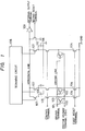
- Fig. 1 is a circuit diagram of a photoelectric transducer apparatus as a line sensor according to a first embodiment of the present invention
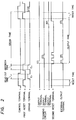
- Fig. 2 is a timing chart for explaining the operation thereof.
- capacitor electrodes 101 of photosensor cells 100 are commonly connected to a driving line, and collector electrodes 102 thereof are commonly connected to a positive voltage terminal.
- a driving terminal is connected to the driving line.
- a pulse signal is applied to the driving terminal to drive the photosensor cells 100.
- Emitter terminals 103 of the photosensor cells 100 are connected to vertical signal lines and commonly connected to each other through reset FETs 104.
- the emitter terminals 103 are connected to a ground terminal GND.
- the gate electrodes of the FETs 104 are commonly connected to a first reset terminal.
- the FETs 104 are switching field effect transistors.
- the vertical signal lines are connected to store capacitors 106 through FETs 105 and to the source electrodes of FETs 107.
- the drain electrodes of the FETs 107 are commonly connected to a horizontal signal line.
- the gate electrodes of the FETs 105 are commonly connected to a control terminal.
- the gate electrodes of the FETs 107 are respectively connected to output terminals of a scanning circuit 108.
- Horizontal signal lines are connected to an external output terminal through an output amplifier 109 and to the ground terminal GND through an FET 100.
- the gate terminal of the FET 110 is connected to a second reset terminal.
- the FET 110 is a field effect transistor for resetting the horizontal line.
- the control and first reset terminals are simultaneously set at H level during the reset time. During the reset time, the optical information stored in the store capacitors 106 is discharged through the FETs 104.
- the optical information stored in the photosensor cells 100 is read out onto the vertical signal lines by applying the readout pulse signal to the driving terminal. Therefore, the optical information is stored in the store capacitors 106.
- the readout pulse signal when the readout pulse signal is set at H level, readout operation of the photosensor cells 100 is started. After the lapse of a predetermined period of time, the readout pulse signal is set at L level, thereby terminating the readout operation.
- the refresh operation state is obtained.
- the optical information stored in the photosensor cells 100 is erased through the FETs 104.
- the store time for storing the carriers in the photosensor cells 100 is defined.
- the signal pulses from the output terminals of the scanning circuit 108 are used to sequentially turn on the FETs 107 according to the shift timings.
- the optical information signals stored in the store capacitors 106 are sequentially read out onto the horizontal lines by horizontal scanning of the scanning circuit 108.
- the readout signals are amplified by the output amplifier 109 and appear at the external output terminal.
- the signal charge is not kept on the vertical signal line for a long period of time, thus reducing blooming and smearing.
- Fig. 3 is a circuit diagram of a photoelectric transducer apparatus according to the second embodiment.
- photosensor cells 1 as the photoelectric transducer elements are one-dimensionally arranged.
- Capacitor electrodes 2 of the photosensor cells 1 are commonly connected to a driving line and to a driving terminal.
- Collector electrodes 3 of the photosensor cells 1 are commonly connected to a positive voltage terminal.
- Emitter electrodes 4 of the photosensor cells 1 are respectively connected to vertical lines 5.
- the vertical lines 5 are commonly connected through FETs 6.
- the FETs 6 are connected to a ground terminal 7.
- the gate electrodes of the FETs 6 are commonly connected to a first reset terminal.
- the capacitors 9 and the source electrodes of the FETs 100 are respectively connected to the vertical lines 5 through FETs 8.
- the capacitors 9 are connected to a ground terminal 12 through a ground line 11.
- the capacitors 9 are signal charge store capacitors, respectively.
- the gate electrodes of the FETs 10 are respectively connected to output terminals 14 of the scanning circuit 13.
- the drain electrodes of the FETs 10 are connected to an output amplifier 16 through a horizontal line 15.
- the output terminal of the output amplifier 16 is connected to an external output terminal 17, so that an output voltage is extracted from the external output terminal 17.
- the gate electrodes of the FETs 10 are respectively connected to the gate electrodes of FETs 18.
- the drain electrodes of the FETs 18 are connected to an output amplifier 20 through an output line 19.
- the output terminal of the output amplifier 20 is connected to an external output terminal 21, so that an output voltage is extracted from the external output terminal 21.
- the source electrodes of the FETs 18 are connected to the vertical lines 5 through FETs 22.
- one electrode of each of capacitors 24 is connected between a corresponding one of the source electrodes of the FETs 18 and a corresponding one of the FETs 22 through a corresponding one of vertical lines 23.
- the other electrode of each of the capacitors 24 is connected to the ground line 11.
- the capacitors 24 serve as dark voltage store capacitors, respectively.
- Reset FETs 26 are connected between the lines 15 and 19 and ground, respectively.
- the gate electrodes of the FETs 26 are connected to the second reset terminal.
- a control circuit 27 supplies timing pulses (Fig. 4) to the respective terminals.
- the photosensor cells store optical information corresponding to the amounts of light upon light store operation during the light irradiation store time.
- the photosensor cells 1 perform store operations of carriers upon light irradiation.
- both the control and first reset terminals are set at H level, so that the charges stored in the capacitors 9 are reset through the corresponding FETs 6.
- the control terminal is set at H level, and the first reset terminal is set at L level.
- a readout pulse voltage is applied to the driving terminal, the optical or light information stored in the photosensor cells 1 is read out onto the vertical lines, and the light information is stored in the capacitors 9.
- the first reset terminal is set at H level and the control terminal is set at L level.
- the refresh pulse voltage is applied to the driving terminal, the photosensor cells 1 are maintained in the refresh state.
- the light information stored in the photosensor cells 1 is erased through the FETs 6.
- the photosensor cells 1 are temporarily shielded from light so that a shading time is started.
- the photosensor cells 1 store the dark voltage generated in the dark state. It should be noted that the dark voltage store time is controlled to be equal to the light irradiation store time.
- both the dark voltage readout terminal and the first reset terminal are set at H level to reset through the FETs 6 the charges stored in the capacitors 24 during the reset time.
- the light information corresponding to the dark voltage components stored in the photosensor cells 1 is read out onto the vertical lines under the following conditions.
- the dark voltage readout terminal is set at H level
- the first reset terminal is set at L level
- the readout pulse voltage Er is applied to the driving terminal. Therefore, the dark voltage signals are stored in the corresponding capacitors 24.
- the dark voltage readout terminal When the dark voltage readout time has elapsed, the dark voltage readout terminal is set at L level, and the first reset terminal is set at H level.
- the refresh pulse voltage E0 is applied, to the driving terminal to set the photosensor cells 1 in the refresh state.
- the refresh pulse voltage applied to the driving terminal is set at L level. Therefore, the refresh time is terminated. Along with this, the shading time is ended, and the first reset terminal is set at L level.
- clocks are supplied to the scanning circuit 13 to sequentially shift the output pulses from the output terminals 14 thereof.
- the FETs 10 and 18 are sequentially turned on in response to these timing pulses.
- the light information signals read out onto the horizontal line 15 are output to the external output terminal 17 through the output amplifier 16.
- the information signals corresponding to the dark voltage components read out onto the output line 19 are output to the external output terminal 21 through the output amplifier 20, so that the output voltage is thus extracted from this external output terminal.
- the readout operation for one horizontal scanning time is completed, and the reset time is started. Thereafter, the above operations will be repeated.
- the actual light information signals simultaneously read out onto the corresponding lines and the information signals corresponding to the dark voltage components are amplified by the output amplifiers 16 and 20 in an output circuit 25, and the amplified signals are extracted through the external output terminals, respectively.
- the present invention is not limited to the above arrangement.
- the output circuit 25 may be replaced with a differential amplifier 28 to subtract the information corresponding to the dark voltage components from the actual light information.
- Light information representing a difference may be output from a terminal 29.
- the dark voltage store time is set to be equal to the light irradiation time.
- such setting need not be performed.
- the dark voltage store time may be set to be shorter than the light irradiation time, and gains of the output amplifiers 16 and 20 in the output circuit 25 may be independently controlled.
- the capacitances of the store capacitors 9 and 24 are adjusted to obtain the same effect as in the above embodiments.
- the photosensor cells are one-dimensionally aligned.
- the arrangement of the cells is not limited to this.
- the photoelectric transducer apparatus comprises light information storing means for storing light information read out from the photoelectric transducer element, and dark voltage storing means for storing a voltage corresponding to the dark voltage component read out from the photoelectric transducer element.
- the actual light information stored in the light information storing means and the information corresponding to the dark voltage component stored in the dark voltage storing means are simultaneously read out from the separate output lines. Therefore, the information corresponding to the dark voltage included in the output can be corrected in units of photosensor cells when the actual optical information read out from the photosensor cell is output, and noise caused by variations in dark voltage can be removed from the output signal.
- an additional external circuit is not required to simplify the system configuration. In addition, demand for an economical photoelectric transducer apparatus can be satisfied.
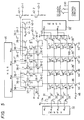
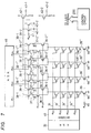
- Fig. 5 is a circuit diagram of photoelectric transducer elements arranged in a 4 x 4 matrix to constitute a photoelectric transducer apparatus.
- the photoelectric transducer apparatus includes: basic photosensor cells 100 (the collector of each bipolar transistor is connected to the substrate and the substrate electrode), horizontal lines 31, 31', 31'', and 31''' serving as the readout-refresh pulse lines; a vertical shift register 32 for generating a readout pulse; buffer MOS transistors 33, 33', 33'', and 33''' arranged between the vertical shift register 32 and the horizontal lines 31, 31', 31'', 31'''; a terminal 34 for applying a pulse ⁇ R to the drains of the buffer MOS transistors 33, 33', 33'', and 33'''; a vertical shift register 32' for generating a refresh pulse; buffer MOS transistors, 47, 47', 47'', and 47''' formed between the vertical shift register 32' and the horizontal lines 31, 31', 31'', and 31'''; a terminal 48 for applying a pulse to the drains of the buffer MOS transistors 47, 47', 47'', and 47''; vertical lines 35,
- the store operation is performed until the t1, and holes corresponding to the amounts of light incident on the photoelectric transducer cells 100 are respectively stored in their p-type base regions.
- a pulse signal ⁇ vc rises to turn on the transistors 44, 44', 44'', and 44'''.
- a pulse signal ⁇ T1 rises to turn on the transistors 36-1, 36-1', 36-1'', and 36-1''' to refresh the store capacitors 37-1, 37-1', 37-1'', and 37-1''.
- a pulse signal ⁇ Hc rises to turn on the transistors 40-1 and 40-2 to refresh the residual charges on the output lines 39-1 and 39-2.
- the pulse signal vc falls to turn off the transistors 44, 44', 44'', and 44''', and the vertical lines 35, 35', 35'', and 35''' and the capacitors 37-1, 37-1', 37-1'', and 37-1''' are set in the floating state.
- a pulse signal ⁇ v1 is output from the vertical shift register 32 to turn on the transistor 33.
- a readout pulse signal ⁇ R is then applied to the terminal 34 and to the horizontal dine 31 through the transistor 33, the readout operation of the photoelectric transducer cells 100 of the first row is started.
- the readout signals from the cells of the first row appear on the vertical lines 35, 35', 35'', and 35''' and in the store capacitors 37-1, 37-1', 37-1'', and 37-1'''.
- the pulse signal ⁇ T1 falls to turn off the transistors 36-1, 36-1', 36-1'', and 36-1'''.
- the capacitors 37-1, 37-1', 37-1'', and 37-1''' and the vertical lines 35, 35', 35'', and 35''' are disconnected, and then the residual charges on the vertical lines 35, 35', 35'', and 35''' are refreshed.
- a pulse signal ⁇ T2 rises to turn on the transistors 36-2, 36-2', 36-2'', and 36-2''' so that the charges in the store capacitors 37-2, 37-2', 37-2'', and 37-2''' are refreshed.
- the pulse signal ⁇ vc falls to turn off the transistors 44, 44', 44'', and 44''.
- a pulse signal ⁇ v2 is output from the vertical shift register 33', and the readout pulse signal ⁇ R is supplied to the horizontal line 31' through the terminal 34. In this state, the readout operation of the photoelectric transducer cells 100 of the second row is started.
- the readout signals from the cells 100 of the second row appear on the vertical lines 35, 35', 35'', and 35''' and in the store capacitors 37-2, 37-2', 37-2'', and 37-2'''.
- the pulse signal T2 falls to turn off the transistors 36-2, 36-2', 36-2'', and 36-2''', and the capacitors 37-2, 37-2', 37-2'', and 37-2''' and the lines 351 35', 35'', and 35''' are disconnected.
- the pulse signal ⁇ vc rises to refresh the residual charges from the vertical lines 35, 35', 35'', and 35'''.
- the pulse signal ⁇ Hc falls to turn off the transistors 40-1 and 40-2.
- the pulse signal ⁇ H1 is output from the horizontal shift register 46 to turn on the transistors 38-1 and 38-2.
- the charges in the capacitors 37-1 and 37-2 are amplified by the transistors 42-1 and 42-2 through the transistors 38-1 and 38-2 and the output lines 39-1 and 39-2.
- the amplified signals appear at the terminals 43-1 and 43-2.
- the pulse signal ⁇ Hc rises to refresh the output lines 39-1 and 39-2.
- the pulse signals ⁇ H2 and ⁇ H3 are sequentially output from the horizontal shift register 46.
- the readout signals from the cell of the first row and the secoond column and the cell of the second row and the second column and the readout signals from the cell of the first row and the third column and the cell of the second row and the third column are sequentially output from the terminals 43-1 and 43-2. Every time the readout signals appear, the output lines 39-1 and 39-2 are refreshed.
- a pulse signal ⁇ c1 is output from the vertical shift register 32' to turn on the transsistors 47 and 47'.
- a pulse signal ⁇ F is applied to the terminal 48 so that the refresh pulse is applied to the horizontal lines 31 and 31' through the transistors 31 and 31'. As a result, the refresh operation of the photoelectric transducer cells 100 of the first and second rows is performed.
- the readout and refresh operations for the cells 100 of the third and fourth rows are performed at time t5 in the same manner as in the cells of the first and second rows.
- the readout and refresh operations are repeated for the cells 100 of the first and second rows at time t6. The above operations are repeated.
- the time required for sending the readout signal onto the vertical line is the period between rising of the pulse signal ⁇ R and falling of the pulse signal ⁇ T1, i.e., between the times t1 and t2 when the output from the photoelectric transducer cell 100 of the first row and the first column is assumed.
- This time interval apparently has a large margin.
- the vertical line selected last by horizontal scanning stores the signal charge for about 52.5 ⁇ s.
- the apparatus of this embodiment can be improved by about 105 times (40 dB) for blooming and smearing, as compared with the conventional apparatus.
- the photosensitive transducer cells are disconnected from the store capacitors by turning off the transistors 36-1, 36-2, 36-1', 36-2', 36-1'', 36-2'', 36-1''', and 36-2''' after the signal charges are stored in the store capacitors, the photoelectric transducer cells 100 can be sufficiently refreshed.
- the refresh time may be a time interval between times t3 and t5, i.e., one horizontal scanning cycle. Therefore, the after image phenomenon can be reduced as compared with the conventional case.
- the number of capacitors is that of the colors of column cells, and the operation as described above is performed. In this case, only one vertical line is used for each column, and the aperture of the sensor cells is not reduced.
- the color filters R, G, and B are arranged according to the Bayer's scheme, and the cells are operated at the timings shown in Fig. 6.
- B signals are stored in the capacitors 37-1 and 37-1''
- G signals are stored in the capacitors 37-2, 37-1', 37-2'', and 37-1'''
- R signals are stored in the capacitors 37-2' and 37-2''', respectively.
- the two vertical lines are simultaneously accessed.
- the number of lines is not limited to two, but can be extended to three or more.
- the number of store capacitors is that of vertical pixels which are simultaneously accessed.
- Fig. 7 is a circuit diagram showing a fifth embodiment of the present invention.
- a decoder 49 is arranged between a vertical shift register 32 and horizontal lines 31, 31', 31'', and 31''', and a control circuit 200 is operated at timings shown in Fig. 8.
- the decoder 49 also serves the function of the photoelectric transducer cell refresh vertical register 46 of the fourth embodiment (Fig. 5), thereby further simplifying the system configuration.
- a pulse signal ⁇ vc has already risen, the vertical lines have already been grounded, and a pulse signal ⁇ T1 rises to refresh the charges of the capacitors 37-1, 37-1', 37-1'', and 37-1''. Thereafter, when the pulse signal ⁇ vc falls to set the vertical lines and the capacitors in the floating state, the decoder 49 outputs a pulse ⁇ D1.
- the signals from the photoelectric transducer cells 100 of the first row appear on the vertical lines and in the capacitors 37-1, 37-1', 37-1'', and 37-1'''.
- the pulse signal ⁇ T1 falls to disconnect the capacitors 37-1, 37-1', 37-1'', and 37-1''' from the vertical lines, and the pulse signal ⁇ vc rises again to refresh the vertical lines.
- the pulse signal ⁇ T2 rises to refresh the capacitors 37-2, 37-2', 37-2'', and 37-2''', and the pulse signal ⁇ vc then falls.
- the pulse signal ⁇ D2 rises again, the signals from the photoelectric transducer cells of the second row appear on the vertical lines and the capacitors 37-2, 37-2', 37-2'', and 37-2'''. Thereafter, the pulse signal ⁇ T2 falls and the pulse signal ⁇ vc rises to refresh the vertical lines. In this state, the signals from the first row are stored in the capacitors 37-1, 37-1', 37-1'', and 37-1''', and the signals from the second row are stored in the capacitors 37-2, 37-2', 37-2'', and 37-2'''.
- these stored signals are sequentially read out from time t3 to time t5.
- the pulse signals ⁇ D1 and ⁇ D2 are set at high level, so that the photoelectric transducer cells 100 of the first and second rows are refreshed.
- the readout and refresh operations of the photoelectric transducer cells of the third and fourth rows are performed in the same manner as described above.
- the refresh and readout operations of the photoelectric transducer cells of each cell are performed by using a single vertical shift register, thereby simplifying the system configuration.
- the two output lines are used.
- the number of output lines may be three or more.
- four output lines are used in units of colors of filters.
- the load of the output lines can be reduced into 1/2 of the two output lines.
- an image processing circuit can also be simplified.
- Fig. 9 The arrangement of Fig. 9 is different from that of Fig. 5 in the following points.
- Output lines 39-3 and 39-4 are added.
- Transistors 38-1 and 38-1''' are connected to a transistor 39-3 instead of the transistor 39-1.
- Transistors 38-2' and 38-2''' are connected to a transistor 39-4 instead of the transistor 39-2.
- Transistors 40-3 and 40-4, the gates of which are commonly connected to the gates of transistors 40-1 and 40-2, are added to refresh the output lines 39-3 and 39-4.
- a transistor 42-3 for outputting a signal from the output signal 39-3, an output terminal 43-4, a transistor 42-4 for outputting a signal from the output line 39-4, and an output terminal 43-4 are added.
- FIG. 9 Other arrangements of Fig. 9 are the same as those of Fig. 5, and the same reference numerals as in Fig. 5 denote the same parts in Fig. 9.
- a plurality of capacitors are arranged for each readout line of the photoelectric transducer cells.
- the signal charges can be stored in the capacitors in a short period of time, and then the readout lines can be disconnected therefrom. Therefore, blooming and smearing caused by the present of the signal charges on the readout lines can be completely prevented.
- the refresh time can be sufficiently prolonged, the after image phenomenon can be effectively prevented.
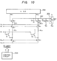
- Fig. 10 is a circuit diagram of a photoelectric transducer apparatus according to the seventh embodiment of the present invention.
- a driving pulse ⁇ R is applied from a control circuit 200 to capacitor electrodes of photoelectric transducer cells S1 to Sn.
- a predetermined positive voltage is applied to the collector electrodes of the cells S1 to Sn.
- the emitter electrodes of the cells S1 to Sn are respectively connected to vertical lines VL1 to VLn. Each of these vertical lines is connected to one terminal of a corresponding one of store capacitors C1 to Cn (each having a capacitance Ct) through a corresponding one of transistors Qt1 to Qtn.
- the other terminal of each of the capacitors C1 to Cn properly receives a bias voltage Vct in a manner to be described later.
- One terminal of each of the capacitors C1 to Cn is connected to an output line 201 through a corresponding one of transistors QS1 and QSn.
- the output line 201 has a stray capacitance Ch equal to the capacitance Ct of each of the store capacitors C1 to Cn.
- the input terminal of an output amplifier 202 is connected to the output line 201 and to a transistor Qrh for properly applying a reset voltage Vrh.
- the value of the reset voltage Vrh is selected within the range wherein the linearity of the output amplifier 202 is not degraded. In this embodiment, the range is 1.5 to 3.5 V.
- the output amplifier 202 is connected to a single power source and is driven thereby.
- Pulses ⁇ h1 to ⁇ hn are sequentially applied from a scanning circuit 103 to the gate electrodes of the transistors QS1 and QSn.
- a pulse ⁇ t is applied to the gate electrodes of the transistors Qt1 to Qtn.
- a voltage Vvc is applied to the respective vertical lines through transistors Qr1 to Qrn.
- the gate electrodes of these transistors receive a pulse ⁇ vc.
- a control circuit 200 supplies a driving pulse of each terminal.
- Fig. 11 is a timing chart for explaining the operation of the control circuit.
- the transistors Qr1 to Qrn and the transistors Qt1 to Qtn are turned on in response to the pulses ⁇ vc and ⁇ t, respectively, to clear (duration T1) the capacitors C1 to Cn. Subsequently, the pulse ⁇ vc is set at L level, and the capacitors C1 to Cn are charged (duration T2) with the readout signals from the photoelectric transducer cells in response to the driving pulse ⁇ r. In this case, the bias voltage Vct is the ground potential.
- the signals from the capacitors C1 to Cn are output at timings of the shift pulses ⁇ h1 to ⁇ hn.
- the transistor QS1 is turned on in response to the pulse ⁇ h1.
- the signal read out from the photoelectric transducer cell S1 and stored in the capacitor C1 is read out onto the output line 201.
- the transistor Qrh is turned on in response to the pulse ⁇ rh, and the output line 201 is reset to the reset voltage Vrh (e.g., +2V).
- Vrh reset voltage
- the readout signals stored in the capacitors C2 to Cn are sequentially read out onto the output line 101 and are output through the output amplifier 102 (a duration T3).
- the refresh operation is performed in response to the pulse ⁇ vc and the driving pulse ⁇ r (a duration T4).
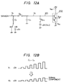
- Fig. 12 A is a circuit diagram for explaining the basic operation of the circuit in Fig. 10, and Fig. 12 B is a timing chart showing the voltage waveforms.
- a switch for selecting the ground voltage (contact A) or the bias voltage of +2V (contact B) is equivalently connected to the store capacitor Ct.
- a switch Qrh for applying the reset voltage Vrh (+2V) is equivalently connected to the output line 201. Also assume that the voltage of the capacitor Ct is v1, and that the voltage of the output line 201 is v2.
- the capacitor Ct is connected to the contact A and grounded, and the readout signal from the sensor is stored in the capacitor Ct.
- the capacitor Ct is then connected to the contact B and receives the bias voltage of +2V.
- the voltage of the capacitor Ct at the time of zero level of the readout signal is set to be equal to the reset voltage of the output line.
- the signal component is input to the output amplifier 102, and the input voltage does not greatly vary upon resetting.
- the dynamic range of the output amplifier 202 can therefore be increased.
- the amplitude of the voltage Vrh or Vct can have a large margin.
- the Vss terminal of the output amplifier 202 can be grounded and a positive voltage (+5V in this case) can be applied to the Vdd terminal thereof by a single power source. (For example, if the reset potential is zero, the negative and positive potentials are respectively applied to the Vss and Vdd terminals, and thus two power sources are required).
- the potential of the output line 201 greatly varies between the reset potential Vrh and the signal component potential of the readout signal.
- the sensor signal is normally amplified to a proper signal level by a signal processor (to be described later). If the above unnecessary component is generated, the circuit system is saturated since the unnecessary component has a magnitude larger than that of the signal component, thereby degrading the signal component. However, according to the above embodiment, the above problem does not occur. If an output amplifier having a wide dynamic range is arranged, it prevents use of a low-level driving source and design of a compact imaging device. However, according this embodiment, the wide dynamic range of the amplifier 202 is not required, so that a compact imaging device can be provided.
- a reset potential portion of the output signal Vout can sufficiently drive a load capacitance (a bonding capacitance, a wiring capacitance, an input transistor capacitance, and the like) by a source current of a source follower circuit.
- the signal component portion of the output signal becomes a sink current of the source follower circuit. If an output resistance is not sufficiently small, a discharge time constant is increased to degrade linearity of a small signal. A decrease in output resistance causes current consumption loss. According to this embodiment, since the dynamic range of the output amplifier can be narrowed, this problem does not occur.
- a sample/hold (S/H) circuit In order to eliminate the unnecessary voltage variation component, a sample/hold (S/H) circuit is required.
- the relationship between a timing pulse for the S/H circuit and the signal component is very important. It is desirable not to arrange the S/H circuit to obtain good temperature characteristics and the power source voltage characteristics. However, if the S/H circuit is not arranged, the blocking characteristic curve of a low-pass filter becomes steep when the output signal is band-limited thereby, and hence image quality is degraded.
- the apparatus of this embodiment can be stably operated against temperature and voltage variations.
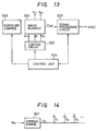
- Fig. 13 shows a schematic arrangement of an imaging device using the above embodiment.
- an imaging element 501 has the same arrangement as in the embodiment of Fig. 10.
- An output signal Vout from the imaging element 501 is gain-controlled by a signal processing circuit 502 and is output as a standard NTSC signal or the like.
- Various pulses ⁇ and the bias voltage Vct for driving the imaging element 501 are generated by a control circuit 200.
- the control circuit 200 is operated under the control of the control unit 504. In this case, the control circuit 200 also serves as the switching means for properly applying the bias voltage Vct.
- the control unit 504 controls the gain or the like of the signal processing circuit 502 on the basis of the output from the imaging element 501 to control the amount of light incident on the imaging element 501.
- the bias voltage Vct applied to the store capacitors C1 to Cn is supplied from the control circuit 200.
- an internal power source 601 shown in Fig. 14, may be arranged.
- the internal power source 601 is operated in response to a control pulse ⁇ ct from the control unit 504 to generate the bias voltage Vct.
- the imaging device can be made more compact at lower power consumption.
Abstract
Description
- The present invention relates to a photoelectric transducer apparatus and, more particularly, to a photoelectric transducer apparatus having a plurality of photoelectric transducer elements each having a capacitor electrode on a control electrode region of a corresponding semiconductor transistor.
- A TV or SV camera with an image sensor such as a CCD or MOS sensor has an aperture mechanism. Photoelectric transducer apparatuses each having a TV or SV camera with an automatic aperture mechanism are described in Japanese Patent Disclosure (Kokai) Nos. 12759/l985 to l2765/l985.
- This photoelectric transducer apparatus includes a photosensor having a plurality of sensor cells each having a capacitor formed on a control electrode of a corresponding semiconductor transistor.
- In the conventional photoelectric transducer apparatus described above, noise is often mixed in an output signal read out from the photosensor cells due to variations in dark voltage generated in the cells within arbitrary store time.
- An output signal corresponding to the dark current component generated within the photosensor cell is prestored as reference optical information in an external memory in a conventional apparatus. A reference output signal derived from the reference optical information and an output signal from the actual optical information read out from the photosensor cell are compared with each other, and the output signal of the actual optical information is corrected, thereby eliminating the noise component caused by the drak voltage.
- In the conventional photoelectric transducer apparatus described above, in order to constitute a photoelectric transducer system, the resultant system is undesirably complicated since a separate external circuit including a noise removal memory is required.
- When a conventional photoelectric transducer apparatus is applied to a video camera or the like, the following problem occurs. When photoelectric transducer cells are arranged in a two-dimensional matrix and scanned in the vertical and horizontal directions, holes are stored in the base of each photoelectric transducer cell in a store mode upon reception of strong light. The base potential is forward-biased with respect to the emitter potential. The potential of a vertical line connected to the emitter electrode of each photoelectric transducer cell receiving strong light is increased to cause a blooming phenomenon. In order to prevent this, it is proposed that the vertical lines are grounded for a period excluding the readout operation, thereby refreshing the charge overflowed onto the vertical line. However, the vertical line can be grounded for only the horizontal blanking period, i.e., about 10 µs. Therefore, the charge overflowed onto the vertical line during the horizontal scanning period still causes the blooming phenomenon.
- In the readout mode, when imade signals are sequentially output by horizontal scanning after they are stored in a vertical line, a dummy signal is generated during the store of the signal in the vertical line. In other words, a smear phenomenon occurs.
- In addition, the period for performing the refresh operation in the conventional apparatus is about 10 µs in the horizontal blanking period. The refresh time is short to result in incomplete refreshing and hence an after image phenomenon.
- Furthermore, assume that when the conventional photoelectric transducer apparatus is used as a single-plate type solid-state imaging device in a color television video camera, color filters are deposited or adhered onto the pixels. If an alignment scheme such as a Bayer alignment is used to form vertical lines in units of colors, i.e., R, G, and B, at least two vertical lines are required for the pixels of each column. In this case, since the vertical line portion does not serve as the photosensitive portion, the light-receiving area is reduced by the two vertical lines for each column. In other words, the opening of the aperture is undesirably reduced.
- In a conventional photosensitive transducer apparatus, negative and positive voltages are required to bias an output amplifier, and the constitution is thus complicated. It is difficult to read out the signal component without degrading the frequency characteristics.
- It is an object of the present invention to provide a photoelectric transducer apparatus capable of solving the conventional drawbacks described above.
- It is another object of the present invention to provide a simple photoelectric transducer apparatus capable of eliminating variations in dark voltage.
- It is still another object of the present invention to provide a photoelectric transducer apparatus comprising optical information storing means for storing optical information read out from a photoelectric transducer element and dark voltage storing means for storing a voltage corresponding to a dark voltage component read out from the photoelectric transducer element, wherein actual optical information stored in the optical information storing means is simultaneously read out together with the dark voltage component stored in the dark voltage storing means onto separate output lines, thereby correcting the information corresponding to the dark voltage in units of optical sensor cells and hence removing noise caused by variations in dark voltage from the output signal from the photosensor cells.
- In order to achieve the above object, according to an aspect of the present invention, there is provided a photoelectric transducer apparatus having a plurality of photoelectric transducer elements each having a capacitor electrode formed on a control electrode of a corresponding semiconductor transistor, the apparatus being adapted to sequentially select each element in units of lines, to control a potential of the control electrode of the selected photoelectric transducer element through the capacitor electrode, to store carriers in the control electrode region, and to read out a signal component corresponding to the amount of charge stored in the control electrode region, comprising: optical information storing means for storing optical information read out from the photoelectric transducer element; and dark voltage storing means for storing a voltage corresponding to a drak voltage read out from the photoelectric transducer element, wherein actual optical information stored in the optical information storing means and information corresponding to the dark voltage component stored in the dark voltage sotring means are simultaneously read out onto different information output lines.
- The information corresponding to the dark voltage component stored in the dark voltage storing means is read out onto the information output line therefor, and at the same time the information corresponding to the dark voltage is corrected in units of photosensor cells, thereby eliminating noise caused by variations in dark voltage.
- The noise corresponding to the dark voltage component can, therefore, be processed within the sensor. An external circuit or the like need not be used to easily constitute a system configuration, thereby obtaining a low-cost photoelectric transducer apparatus.
- It is still another object of the present invention to provide an imaging element and an apparatus using the same, wherein the after image, blooming, and smearing can be prevented with a simple construction.
- It is still another object of the present invention to provide a color imaging element having a large aperture.
- In order to achieve these objects, according to another aspect of the present invention, there is provided a photoelectric transducer apparatus comprising:
a plurality of photoelectric transducer cells;
a signal read line for reading out signals from the plurality of photoelectric transducer elements; and
a plurality of capacitors for selectively storing the signals read out through the signal read line. - According to this aspect of the present invention, since the plurality of capacitors for selectively storing the signals read out through the signal read line are provided, the image signal appearing on the vertical line can be shortened , thereby reducing the frequency of occurrence of the blooming and smearing phenomena. Since the capacitor can be disconnected from the pixel after the image signal is stored in the capacitor, the refresh time can be prolonged to reduce the occurrence of the after image phenomenon. In addition, if the photoelectric transducer apparatus is used in a color video camera, the number of capacitors can be that of the color signals of the row pixels, and only one vertical line is used, thereby increasing the aperture.
- It is still another object of the present invention to provide a photoelectric transducer apparatus wherein a single power source can be used without degrading the signal component of the read signal.
- In order to achieve the above object, according to still another aspect of the present invention, there is provided a photoelectric transducer apparatus for reading output a read signal from a photoelectric transducer element through an amplifier after the read signal is temporarily stored in a storing means, comprising switching means for properly applying a bias voltage to the storing means.
- With the above arrangement, the reference potential of the store capacitor can be properly changed to use a single power source without degrading the signal component of the read signal.
- It is still another object of the present invention to provide a photoelectric transducer apparatus little subjected to smearing or blooming.
- In order to achieve the above object, according to still another aspect of the present invention, a capacitor is arranged in a vertical signal line through a switch to store the signal from the photoelectric transducer cell in the capacitor, thereby resetting the vertical signal line, so that the signal component in the capacitor is free from smearing or blooming.
-
- Fig. 1 is a circuit diagram of a photoelectric transducer apparatus according to a first embodiment of the present invention;
- Fig. 2 is a timing chart for explaining the operation of the apparatus in Fig. 1;
- Fig. 3A is a circuit diagram of a photoelectric transducer apparatus according to a second embodiment of the present invention;
- Fig. 3B is a circuit diagram showing the main part of a third embodiment;
- Fig. 4 is a timing chart for explaining the operation of the second and third embodiments of the present invention;
- Fig. 5 is a circuit diagram of a photoelectric transducer apparatus according to a fourth embodiment of the present invention;
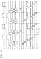
- Fig. 6 is a timing chart for explaining the operation of the apparatus in Fig. 5;
- Fig. 7 is a circuit diagram of a photoelectric transducer apparatus according to a fifth embodiment of the present invention;
- Fig. 8 is a timing chart for explaining the operation of the apparatus in Fig. 7;
- Fig. 9 is a circuit diagram of a photoelectric transducer apparatus according to a sixth embodiment of the present invention;
- Fig. 10 is a circuit diagram of a photoelectric transducer apparatus according to a seventh embodiment of the present invention;
- Fig. 11 is a timing chart for explaining the apparatus in Fig. 10;
- Fig. 12 A is a circuit diagram for explaining a basic operation of the seventh embodiment of the present invention;
- Fig. 12 B is a timing chart showing the voltage waveforms in the seventh embodiment;
- Fig. 13 is a block diagram of an imaging device on the basis of the above embodiments of the present invention; and
- Fig. 14 is a circuit diagram showing part of an eighth embodiment of the present invention.
- Fig. 1 is a circuit diagram of a photoelectric transducer apparatus as a line sensor according to a first embodiment of the present invention, and Fig. 2 is a timing chart for explaining the operation thereof.
- Referring to Figs. 1 and 2,
capacitor electrodes 101 ofphotosensor cells 100 are commonly connected to a driving line, andcollector electrodes 102 thereof are commonly connected to a positive voltage terminal. - A driving terminal is connected to the driving line.
- A pulse signal is applied to the driving terminal to drive the
photosensor cells 100. Emitter terminals 103 of thephotosensor cells 100 are connected to vertical signal lines and commonly connected to each other throughreset FETs 104. The emitter terminals 103 are connected to a ground terminal GND. - The gate electrodes of the
FETs 104 are commonly connected to a first reset terminal. - The
FETs 104 are switching field effect transistors. - The vertical signal lines are connected to store
capacitors 106 throughFETs 105 and to the source electrodes ofFETs 107. The drain electrodes of theFETs 107 are commonly connected to a horizontal signal line. The gate electrodes of theFETs 105 are commonly connected to a control terminal. - The gate electrodes of the
FETs 107 are respectively connected to output terminals of ascanning circuit 108. - Horizontal signal lines are connected to an external output terminal through an
output amplifier 109 and to the ground terminal GND through anFET 100. - The gate terminal of the
FET 110 is connected to a second reset terminal. - The
FET 110 is a field effect transistor for resetting the horizontal line. - The operation of the circuit in Fig. 1 will be described with reference to a timing chart in Fig. 2.
- The control and first reset terminals are simultaneously set at H level during the reset time. During the reset time, the optical information stored in the
store capacitors 106 is discharged through theFETs 104. - When the control terminal is set at H level and the first reset terminal is set at L level, the optical information stored in the
photosensor cells 100 is read out onto the vertical signal lines by applying the readout pulse signal to the driving terminal. Therefore, the optical information is stored in thestore capacitors 106. - In this manner, when the readout pulse signal is set at H level, readout operation of the
photosensor cells 100 is started. After the lapse of a predetermined period of time, the readout pulse signal is set at L level, thereby terminating the readout operation. - When the control terminal is set at L level, and the first reset and driving terminals are set at H level, the refresh operation state is obtained. The optical information stored in the
photosensor cells 100 is erased through theFETs 104. - When the refresh pulse signal is set at L level, the refresh operation is ended.
- Thereafter, during the period until the readout operation state is obtained again, the store time for storing the carriers in the
photosensor cells 100 is defined. - The signal pulses from the output terminals of the
scanning circuit 108 are used to sequentially turn on theFETs 107 according to the shift timings. - The optical information signals stored in the
store capacitors 106 are sequentially read out onto the horizontal lines by horizontal scanning of thescanning circuit 108. The readout signals are amplified by theoutput amplifier 109 and appear at the external output terminal. - When all optical information signals stored in the
store capacitors 106 are read out completely, the reset time is initialized again. - The above operations are thus repeated.
- With the above arrangement, the signal charge is not kept on the vertical signal line for a long period of time, thus reducing blooming and smearing.
- A second embodiment of the present invention will be described with reference to the accompanying drawings.
- Fig. 3 is a circuit diagram of a photoelectric transducer apparatus according to the second embodiment.
- Referring to Fig. 3,
photosensor cells 1 as the photoelectric transducer elements are one-dimensionally arranged. -
Capacitor electrodes 2 of thephotosensor cells 1 are commonly connected to a driving line and to a driving terminal.Collector electrodes 3 of thephotosensor cells 1 are commonly connected to a positive voltage terminal. -
Emitter electrodes 4 of thephotosensor cells 1 are respectively connected tovertical lines 5. Thevertical lines 5 are commonly connected through FETs 6. The FETs 6 are connected to aground terminal 7. - The gate electrodes of the FETs 6 are commonly connected to a first reset terminal.
- The
capacitors 9 and the source electrodes of theFETs 100 are respectively connected to thevertical lines 5 throughFETs 8. Thecapacitors 9 are connected to aground terminal 12 through aground line 11. - The
capacitors 9 are signal charge store capacitors, respectively. - The gate electrodes of the
FETs 10 are respectively connected tooutput terminals 14 of thescanning circuit 13. The drain electrodes of theFETs 10 are connected to anoutput amplifier 16 through ahorizontal line 15. The output terminal of theoutput amplifier 16 is connected to anexternal output terminal 17, so that an output voltage is extracted from theexternal output terminal 17. - The gate electrodes of the
FETs 10 are respectively connected to the gate electrodes ofFETs 18. The drain electrodes of theFETs 18 are connected to anoutput amplifier 20 through anoutput line 19. - The output terminal of the
output amplifier 20 is connected to anexternal output terminal 21, so that an output voltage is extracted from theexternal output terminal 21. - The source electrodes of the
FETs 18 are connected to thevertical lines 5 throughFETs 22. - In the above embodiment, one electrode of each of
capacitors 24 is connected between a corresponding one of the source electrodes of theFETs 18 and a corresponding one of theFETs 22 through a corresponding one ofvertical lines 23. The other electrode of each of thecapacitors 24 is connected to theground line 11. - The
capacitors 24 serve as dark voltage store capacitors, respectively.Reset FETs 26 are connected between thelines FETs 26 are connected to the second reset terminal. Acontrol circuit 27 supplies timing pulses (Fig. 4) to the respective terminals. - The operation of the above embodiment will be described below.
- As shown in the timing chart of Fig. 4, the photosensor cells store optical information corresponding to the amounts of light upon light store operation during the light irradiation store time.
- During a predetermined period of time until the light information readout, the
photosensor cells 1 perform store operations of carriers upon light irradiation. During the reset time, both the control and first reset terminals are set at H level, so that the charges stored in thecapacitors 9 are reset through the corresponding FETs 6. - The control terminal is set at H level, and the first reset terminal is set at L level. When a readout pulse voltage is applied to the driving terminal, the optical or light information stored in the
photosensor cells 1 is read out onto the vertical lines, and the light information is stored in thecapacitors 9. - When the light information readout time has elapsed, the first reset terminal is set at H level and the control terminal is set at L level. In this state, when the refresh pulse voltage is applied to the driving terminal, the
photosensor cells 1 are maintained in the refresh state. The light information stored in thephotosensor cells 1 is erased through the FETs 6. - When the refresh time has elapsed, the
photosensor cells 1 are temporarily shielded from light so that a shading time is started. - In this case, the
photosensor cells 1 store the dark voltage generated in the dark state. It should be noted that the dark voltage store time is controlled to be equal to the light irradiation store time. - Subsequently, both the dark voltage readout terminal and the first reset terminal are set at H level to reset through the FETs 6 the charges stored in the
capacitors 24 during the reset time. - The light information corresponding to the dark voltage components stored in the
photosensor cells 1 is read out onto the vertical lines under the following conditions. The dark voltage readout terminal is set at H level, the first reset terminal is set at L level, and the readout pulse voltage Er is applied to the driving terminal. Therefore, the dark voltage signals are stored in the correspondingcapacitors 24. - When the dark voltage readout time has elapsed, the dark voltage readout terminal is set at L level, and the first reset terminal is set at H level. The refresh pulse voltage E0 is applied, to the driving terminal to set the
photosensor cells 1 in the refresh state. - When a predetermined period of time has elapsed, the refresh pulse voltage applied to the driving terminal is set at L level. Therefore, the refresh time is terminated. Along with this, the shading time is ended, and the first reset terminal is set at L level.
- Subsequently, clocks are supplied to the
scanning circuit 13 to sequentially shift the output pulses from theoutput terminals 14 thereof. TheFETs - By this horizontal scanning, light information signals are sequentially read out from the
capacitors 9 onto thehorizontal line 15. In synchronism with the readout operation, the information signals corresponding to the dark voltage components stored in thecapacitors 24 are read out onto theoutput line 19. - In this manner, the light information signals read out onto the
horizontal line 15 are output to theexternal output terminal 17 through theoutput amplifier 16. The information signals corresponding to the dark voltage components read out onto theoutput line 19 are output to theexternal output terminal 21 through theoutput amplifier 20, so that the output voltage is thus extracted from this external output terminal. - For example, the readout operation for one horizontal scanning time is completed, and the reset time is started. Thereafter, the above operations will be repeated.
- Since the photoelectric transducer apparatus of this embodiment is operated as described above, an additional external circuit which was required in the conventional photoelectric transducer apparatus to remove the noise component caused by the dark voltage need not be used, thereby smplifying the system configuration. Therefore, demand for a low-cost photoelectric transducer apparatus can be satisfied.
- In the above embodiment, the actual light information signals simultaneously read out onto the corresponding lines and the information signals corresponding to the dark voltage components are amplified by the
output amplifiers output circuit 25, and the amplified signals are extracted through the external output terminals, respectively. However, the present invention is not limited to the above arrangement. As shown in Fig. 3, (a third embodiment), theoutput circuit 25 may be replaced with adifferential amplifier 28 to subtract the information corresponding to the dark voltage components from the actual light information. Light information representing a difference may be output from a terminal 29. - In the second and third embodiments, the dark voltage store time is set to be equal to the light irradiation time. However, such setting need not be performed.
- For example, by effectively utilizing the relationship between the dark voltage store time and the amount of dark voltage components generated by the
photosensor cells 1, i.e., a substantially proportional relationship, the dark voltage store time may be set to be shorter than the light irradiation time, and gains of theoutput amplifiers output circuit 25 may be independently controlled. Alternatively, the capacitances of thestore capacitors - In the second and third embodiments, the photosensor cells are one-dimensionally aligned. However, the arrangement of the cells is not limited to this.
- As described above, the photoelectric transducer apparatus comprises light information storing means for storing light information read out from the photoelectric transducer element, and dark voltage storing means for storing a voltage corresponding to the dark voltage component read out from the photoelectric transducer element. The actual light information stored in the light information storing means and the information corresponding to the dark voltage component stored in the dark voltage storing means are simultaneously read out from the separate output lines. Therefore, the information corresponding to the dark voltage included in the output can be corrected in units of photosensor cells when the actual optical information read out from the photosensor cell is output, and noise caused by variations in dark voltage can be removed from the output signal. Unlike in the conventional photoelectric transducer apparatus, an additional external circuit is not required to simplify the system configuration. In addition, demand for an economical photoelectric transducer apparatus can be satisfied.
- A fourth embodiment of the present invention will be described in detail with reference to the accompanying drawings.
- Fig. 5 is a circuit diagram of photoelectric transducer elements arranged in a 4 x 4 matrix to constitute a photoelectric transducer apparatus.
- The photoelectric transducer apparatus includes: basic photosensor cells 100 (the collector of each bipolar transistor is connected to the substrate and the substrate electrode), horizontal lines 31, 31', 31'', and 31''' serving as the readout-refresh pulse lines; a vertical shift register 32 for generating a readout pulse; buffer MOS transistors 33, 33', 33'', and 33''' arranged between the vertical shift register 32 and the horizontal lines 31, 31', 31'', 31'''; a terminal 34 for applying a pulse φR to the drains of the buffer MOS transistors 33, 33', 33'', and 33'''; a vertical shift register 32' for generating a refresh pulse; buffer MOS transistors, 47, 47', 47'', and 47''' formed between the vertical shift register 32' and the horizontal lines 31, 31', 31'', and 31'''; a terminal 48 for applying a pulse to the drains of the buffer MOS transistors 47, 47', 47'', and 47'''; vertical lines 35, 35', 35'', and 35''' serving as vertical readout lines for reading out signal charges from the basic photosensor cells 100; capacitors 37-1, 37-2, 37-1', 37-2', 37-1'', 37-2'', 37-1''', and 37-2''' for storing these signal charges; transfer MOS transistors 36-1, 36-2, 36-1', 36-2', 36-1'', 36-2'', 36-1''', and 36-2''' arranged between the vertical lines 35, 35', 35'', and 35''' and the capacitors 37-1, 37-2, 37-1', 37-2', 37-1'', 37-2'', 37-1''', and 37-2'''; a horizontal shift register 46 for generating a pulse for selecting each store capacitor; gate MOS transistors 38-1, 38-2, 38-1', 38-2', 38-1'', 38-2'', 38-1''', and 38-2''' for charging/discharging the store capacitors 37-1, 37-2, 37-1', 37-2', 37-1'', 37-2'', 37-1''', and 37-2'''; output lines 39-1 and 39-2 for reading out the store voltages and supplying them to an amplifier; MOS transistors 40-1 and 40-2 for refreshing the charges on the readout lines; a terminal 41 for applying the refresh pulse to the MOS transistors 40-1 and 40-2; transistors 42-1 and 42-2 such as bipolar transistors, MOSFETs or JFETs for amplifying the output signals; output terminals 43-1 and 43-2 of the transistors 42-1 and 42-2; MOS transistors 44, 44', 44'', and 44''' for refreshing the charges stored on the vertical lines 35, 35', 35'', and 35'''; a terminal 45 for supplying a pulse to the gates of the MOS transistors 44, 44', 44'', and 44'''; a horizontal shift register 46 for turning on the MOS transistors 38-1, 38-2, 38-1', 38-2', 38-1'', 38-2'', 38-1''', and 38-2'''; and a control circuit 200 for supplying signals to the respective terminals.
- The operation of the photoelectric transducer apparatus will be described with reference to Fig. 5 and a timing chart of Fig. 6.
- Assume that the collector potential of the photosensor cells is kept at a positive potential in the following description.
- The store operation is performed until the t1, and holes corresponding to the amounts of light incident on the
photoelectric transducer cells 100 are respectively stored in their p-type base regions. - At time t1, a pulse signal φvc rises to turn on the
transistors 44, 44', 44'', and 44'''. A pulse signal φT1 rises to turn on the transistors 36-1, 36-1', 36-1'', and 36-1''' to refresh the store capacitors 37-1, 37-1', 37-1'', and 37-1'''. A pulse signal φHc rises to turn on the transistors 40-1 and 40-2 to refresh the residual charges on the output lines 39-1 and 39-2. Subsequently, the pulse signal vc falls to turn off thetransistors 44, 44', 44'', and 44''', and thevertical lines 35, 35', 35'', and 35''' and the capacitors 37-1, 37-1', 37-1'', and 37-1''' are set in the floating state. A pulse signal φv1 is output from thevertical shift register 32 to turn on thetransistor 33. When a readout pulse signal φR is then applied to the terminal 34 and to thehorizontal dine 31 through thetransistor 33, the readout operation of thephotoelectric transducer cells 100 of the first row is started. By this readout operation, the readout signals from the cells of the first row appear on thevertical lines 35, 35', 35'', and 35''' and in the store capacitors 37-1, 37-1', 37-1'', and 37-1'''. When the readout operation is completed, the pulse signal φT1 falls to turn off the transistors 36-1, 36-1', 36-1'', and 36-1'''. The capacitors 37-1, 37-1', 37-1'', and 37-1''' and thevertical lines 35, 35', 35'', and 35''' are disconnected, and then the residual charges on thevertical lines 35, 35', 35'', and 35''' are refreshed. - At time t2, a pulse signal φT2 rises to turn on the transistors 36-2, 36-2', 36-2'', and 36-2''' so that the charges in the store capacitors 37-2, 37-2', 37-2'', and 37-2''' are refreshed. Subsequently, the pulse signal φvc falls to turn off the
transistors 44, 44', 44'', and 44'''. A pulse signal φv2 is output from the vertical shift register 33', and the readout pulse signal φR is supplied to the horizontal line 31' through the terminal 34. In this state, the readout operation of thephotoelectric transducer cells 100 of the second row is started. By this readout operation, the readout signals from thecells 100 of the second row appear on thevertical lines 35, 35', 35'', and 35''' and in the store capacitors 37-2, 37-2', 37-2'', and 37-2'''. Upon completion of the readout operation for the second row, the pulse signal T2 falls to turn off the transistors 36-2, 36-2', 36-2'', and 36-2''', and the capacitors 37-2, 37-2', 37-2'', and 37-2''' and the lines 351 35', 35'', and 35''' are disconnected. The pulse signal φvc rises to refresh the residual charges from thevertical lines 35, 35', 35'', and 35'''. - At time t3, the pulse signal φHc falls to turn off the transistors 40-1 and 40-2. The pulse signal φH1 is output from the
horizontal shift register 46 to turn on the transistors 38-1 and 38-2. The charges in the capacitors 37-1 and 37-2 are amplified by the transistors 42-1 and 42-2 through the transistors 38-1 and 38-2 and the output lines 39-1 and 39-2. The amplified signals appear at the terminals 43-1 and 43-2. When this output operation is completed, the pulse signal φHc rises to refresh the output lines 39-1 and 39-2. Sub-sequently, the pulse signals φH2 and φH3 are sequentially output from thehorizontal shift register 46. In the same manner as described above, the readout signals from the cell of the first row and the secoond column and the cell of the second row and the second column and the readout signals from the cell of the first row and the third column and the cell of the second row and the third column are sequentially output from the terminals 43-1 and 43-2. Every time the readout signals appear, the output lines 39-1 and 39-2 are refreshed. - At time t4, a pulse signal φc1 is output from the vertical shift register 32' to turn on the
transsistors 47 and 47'. A pulse signal φF is applied to the terminal 48 so that the refresh pulse is applied to thehorizontal lines 31 and 31' through thetransistors 31 and 31'. As a result, the refresh operation of thephotoelectric transducer cells 100 of the first and second rows is performed. - The readout and refresh operations for the
cells 100 of the third and fourth rows are performed at time t5 in the same manner as in the cells of the first and second rows. The readout and refresh operations are repeated for thecells 100 of the first and second rows at time t6. The above operations are repeated. - In the above operation, the time required for sending the readout signal onto the vertical line is the period between rising of the pulse signal φR and falling of the pulse signal φT1, i.e., between the times t1 and t2 when the output from the
photoelectric transducer cell 100 of the first row and the first column is assumed. This time interval apparently has a large margin. In the conventional photoelectric transducer apparatus applied in the video camera, the vertical line selected last by horizontal scanning stores the signal charge for about 52.5 µs. For example, if the time interval between rising of the pulse signal φR and falling of the pulse signal φT1 is set to be 0.5 µs, the apparatus of this embodiment can be improved by about 105 times (40 dB) for blooming and smearing, as compared with the conventional apparatus. - Since the store capacitors are arranged, the photosensitive transducer cells are disconnected from the store capacitors by turning off the transistors 36-1, 36-2, 36-1', 36-2', 36-1'', 36-2'', 36-1''', and 36-2''' after the signal charges are stored in the store capacitors, the
photoelectric transducer cells 100 can be sufficiently refreshed. For example, the refresh time may be a time interval between times t3 and t5, i.e., one horizontal scanning cycle. Therefore, the after image phenomenon can be reduced as compared with the conventional case. - If the photoelectric transducer apparatus is applied to a color video camera and color filters are formed on the sensor cells, the number of capacitors is that of the colors of column cells, and the operation as described above is performed. In this case, only one vertical line is used for each column, and the aperture of the sensor cells is not reduced. For example, as shown in Fig. 5, the color filters R, G, and B are arranged according to the Bayer's scheme, and the cells are operated at the timings shown in Fig. 6. B signals are stored in the capacitors 37-1 and 37-1'', G signals are stored in the capacitors 37-2, 37-1', 37-2'', and 37-1''', and R signals are stored in the capacitors 37-2' and 37-2''', respectively.
- In the above embodiment, the two vertical lines are simultaneously accessed. However, the number of lines is not limited to two, but can be extended to three or more. In this case, the number of store capacitors is that of vertical pixels which are simultaneously accessed.
- Fig. 7 is a circuit diagram showing a fifth embodiment of the present invention. A
decoder 49 is arranged between avertical shift register 32 andhorizontal lines 31, 31', 31'', and 31''', and acontrol circuit 200 is operated at timings shown in Fig. 8. - In this embodiment, the
decoder 49 also serves the function of the photoelectric transducer cell refreshvertical register 46 of the fourth embodiment (Fig. 5), thereby further simplifying the system configuration. - The operation of the fifth embodiment will be described with reference to the timing chart of Fig. 8. Assume that the store operaiton is performed until time t1, and that the holes corresponding to the amounts of light incident on the
photoelectric transducer cells 100 are respectively stored in their p-type base regions. - At time t1, a pulse signal φvc has already risen, the vertical lines have already been grounded, and a pulse signal φT1 rises to refresh the charges of the capacitors 37-1, 37-1', 37-1'', and 37-1'''. Thereafter, when the pulse signal φvc falls to set the vertical lines and the capacitors in the floating state, the
decoder 49 outputs a pulse φD1. - The signals from the
photoelectric transducer cells 100 of the first row appear on the vertical lines and in the capacitors 37-1, 37-1', 37-1'', and 37-1'''. After the readout operation is completed, the pulse signal φT1 falls to disconnect the capacitors 37-1, 37-1', 37-1'', and 37-1''' from the vertical lines, and the pulse signal φvc rises again to refresh the vertical lines. The pulse signal φT2 rises to refresh the capacitors 37-2, 37-2', 37-2'', and 37-2''', and the pulse signal φvc then falls. When the pulse signal φD2 rises again, the signals from the photoelectric transducer cells of the second row appear on the vertical lines and the capacitors 37-2, 37-2', 37-2'', and 37-2'''. Thereafter, the pulse signal φT2 falls and the pulse signal φvc rises to refresh the vertical lines. In this state, the signals from the first row are stored in the capacitors 37-1, 37-1', 37-1'', and 37-1''', and the signals from the second row are stored in the capacitors 37-2, 37-2', 37-2'', and 37-2'''. - In the same manner as in the first embodiment, these stored signals are sequentially read out from time t3 to time t5. In this case, during the time interval from time t4 to time immediately before time t5, the pulse signals φD1 and φD2 are set at high level, so that the
photoelectric transducer cells 100 of the first and second rows are refreshed. - The readout and refresh operations of the photoelectric transducer cells of the third and fourth rows are performed in the same manner as described above.
- According to this embodiment, the refresh and readout operations of the photoelectric transducer cells of each cell are performed by using a single vertical shift register, thereby simplifying the system configuration.
- In the above embodiment, the two output lines are used. However, the number of output lines may be three or more. For example, as shown in a sixth embodiment of Fig. 9, four output lines are used in units of colors of filters. In this case, the load of the output lines can be reduced into 1/2 of the two output lines. In addition, an image processing circuit can also be simplified.
- The arrangement of Fig. 9 is different from that of Fig. 5 in the following points. Output lines 39-3 and 39-4 are added. Transistors 38-1 and 38-1''' are connected to a transistor 39-3 instead of the transistor 39-1. Transistors 38-2' and 38-2''' are connected to a transistor 39-4 instead of the transistor 39-2. Transistors 40-3 and 40-4, the gates of which are commonly connected to the gates of transistors 40-1 and 40-2, are added to refresh the output lines 39-3 and 39-4. A transistor 42-3 for outputting a signal from the output signal 39-3, an output terminal 43-4, a transistor 42-4 for outputting a signal from the output line 39-4, and an output terminal 43-4 are added.
- Other arrangements of Fig. 9 are the same as those of Fig. 5, and the same reference numerals as in Fig. 5 denote the same parts in Fig. 9.
- In the photoelectric transducer apparatuses in the foruth to sixth embodiments as described above in detail, a plurality of capacitors are arranged for each readout line of the photoelectric transducer cells. The signal charges can be stored in the capacitors in a short period of time, and then the readout lines can be disconnected therefrom. Therefore, blooming and smearing caused by the present of the signal charges on the readout lines can be completely prevented.
- Furthermore, since the refresh time can be sufficiently prolonged, the after image phenomenon can be effectively prevented.
- Many lines are often simultaneously accessed when the photoelectric transducer apparatus is applied to a color video camera or the like. The capacitors corresponding to the pixels to be accessed are arranged for each readout line. The number of readout lines need not be increased, and thus the aperture can be increased.
- A seventh embodiment of the present invention will be described below.
- Fig. 10 is a circuit diagram of a photoelectric transducer apparatus according to the seventh embodiment of the present invention.
- Referring to Fig. 10, a driving pulse φR is applied from a
control circuit 200 to capacitor electrodes of photoelectric transducer cells S1 to Sn. A predetermined positive voltage is applied to the collector electrodes of the cells S1 to Sn. The emitter electrodes of the cells S1 to Sn are respectively connected to vertical lines VL1 to VLn. Each of these vertical lines is connected to one terminal of a corresponding one of store capacitors C1 to Cn (each having a capacitance Ct) through a corresponding one of transistors Qt1 to Qtn. The other terminal of each of the capacitors C1 to Cn properly receives a bias voltage Vct in a manner to be described later. - One terminal of each of the capacitors C1 to Cn is connected to an
output line 201 through a corresponding one of transistors QS1 and QSn. Theoutput line 201 has a stray capacitance Ch equal to the capacitance Ct of each of the store capacitors C1 to Cn. - The input terminal of an
output amplifier 202 is connected to theoutput line 201 and to a transistor Qrh for properly applying a reset voltage Vrh. The value of the reset voltage Vrh is selected within the range wherein the linearity of theoutput amplifier 202 is not degraded. In this embodiment, the range is 1.5 to 3.5 V. Theoutput amplifier 202 is connected to a single power source and is driven thereby. - Pulses φh1 to φhn are sequentially applied from a scanning circuit 103 to the gate electrodes of the transistors QS1 and QSn. A pulse φt is applied to the gate electrodes of the transistors Qt1 to Qtn.
- A voltage Vvc is applied to the respective vertical lines through transistors Qr1 to Qrn. The gate electrodes of these transistors receive a pulse φvc. A
control circuit 200 supplies a driving pulse of each terminal. Fig. 11 is a timing chart for explaining the operation of the control circuit. - The transistors Qr1 to Qrn and the transistors Qt1 to Qtn are turned on in response to the pulses φvc and φt, respectively, to clear (duration T1) the capacitors C1 to Cn. Subsequently, the pulse φvc is set at L level, and the capacitors C1 to Cn are charged (duration T2) with the readout signals from the photoelectric transducer cells in response to the driving pulse φr. In this case, the bias voltage Vct is the ground potential.
- After the bias voltage Vct is set to be +2V, the signals from the capacitors C1 to Cn are output at timings of the shift pulses φh1 to φhn.
- More specifically, the transistor QS1 is turned on in response to the pulse φh1. As described above, the signal read out from the photoelectric transducer cell S1 and stored in the capacitor C1 is read out onto the
output line 201. Subsequently, the transistor Qrh is turned on in response to the pulse φrh, and theoutput line 201 is reset to the reset voltage Vrh (e.g., +2V). In the same manner as described above, the readout signals stored in the capacitors C2 to Cn are sequentially read out onto theoutput line 101 and are output through the output amplifier 102 (a duration T3). - When the output operation is completed, the refresh operation is performed in response to the pulse φvc and the driving pulse φr (a duration T4).
- The basic operation of the circuit in Fig. 10 will be described below.
- Fig. 12 A is a circuit diagram for explaining the basic operation of the circuit in Fig. 10, and Fig. 12 B is a timing chart showing the voltage waveforms.
- Referring to Fig. 12 A , a switch for selecting the ground voltage (contact A) or the bias voltage of +2V (contact B) is equivalently connected to the store capacitor Ct. A switch Qrh for applying the reset voltage Vrh (+2V) is equivalently connected to the
output line 201. Also assume that the voltage of the capacitor Ct is v1, and that the voltage of theoutput line 201 is v2. - The capacitor Ct is connected to the contact A and grounded, and the readout signal from the sensor is stored in the capacitor Ct. The capacitor Ct is then connected to the contact B and receives the bias voltage of +2V. The voltage of the capacitor Ct at the time of zero level of the readout signal is set to be equal to the reset voltage of the output line.
- Subsequently, when the switch Qs is closed, the 1/2 component of the signal of the voltage v1 appears on the
output line 201 since
output amplifier 202. Closing of the switch Qrh causes resetting of theoutput line 201 at the voltage of +2V (Fig. 12 B ). - According to this embodiment, only the signal component is input to the
output amplifier 102, and the input voltage does not greatly vary upon resetting. The dynamic range of theoutput amplifier 202 can therefore be increased. The amplitude of the voltage Vrh or Vct can have a large margin. - By setting the potential of the
output line 201 connected to the input terminal of theoutput amplifier 202 at a low potential excluding the ground potential, the Vss terminal of theoutput amplifier 202 can be grounded and a positive voltage (+5V in this case) can be applied to the Vdd terminal thereof by a single power source. (For example, if the reset potential is zero, the negative and positive potentials are respectively applied to the Vss and Vdd terminals, and thus two power sources are required). - If the bias voltage of the capacitor Ct is not changed, the potential of the
output line 201 greatly varies between the reset potential Vrh and the signal component potential of the readout signal. The sensor signal is normally amplified to a proper signal level by a signal processor (to be described later). If the above unnecessary component is generated, the circuit system is saturated since the unnecessary component has a magnitude larger than that of the signal component, thereby degrading the signal component. However, according to the above embodiment, the above problem does not occur. If an output amplifier having a wide dynamic range is arranged, it prevents use of a low-level driving source and design of a compact imaging device. However, according this embodiment, the wide dynamic range of theamplifier 202 is not required, so that a compact imaging device can be provided. - Now assume the charge/discharge time. A reset potential portion of the output signal Vout can sufficiently drive a load capacitance (a bonding capacitance, a wiring capacitance, an input transistor capacitance, and the like) by a source current of a source follower circuit. However, the signal component portion of the output signal becomes a sink current of the source follower circuit. If an output resistance is not sufficiently small, a discharge time constant is increased to degrade linearity of a small signal. A decrease in output resistance causes current consumption loss. According to this embodiment, since the dynamic range of the output amplifier can be narrowed, this problem does not occur.
- In order to eliminate the unnecessary voltage variation component, a sample/hold (S/H) circuit is required. The relationship between a timing pulse for the S/H circuit and the signal component is very important. It is desirable not to arrange the S/H circuit to obtain good temperature characteristics and the power source voltage characteristics. However, if the S/H circuit is not arranged, the blocking characteristic curve of a low-pass filter becomes steep when the output signal is band-limited thereby, and hence image quality is degraded. However, according to this embodiment, since the S/H circuit need not be used, the apparatus of this embodiment can be stably operated against temperature and voltage variations.
- Fig. 13 shows a schematic arrangement of an imaging device using the above embodiment.
- Referring to Fig. 13, an
imaging element 501 has the same arrangement as in the embodiment of Fig. 10. An output signal Vout from theimaging element 501 is gain-controlled by asignal processing circuit 502 and is output as a standard NTSC signal or the like. - Various pulses φ and the bias voltage Vct for driving the
imaging element 501 are generated by acontrol circuit 200. Thecontrol circuit 200 is operated under the control of thecontrol unit 504. In this case, thecontrol circuit 200 also serves as the switching means for properly applying the bias voltage Vct. Thecontrol unit 504 controls the gain or the like of thesignal processing circuit 502 on the basis of the output from theimaging element 501 to control the amount of light incident on theimaging element 501. - The bias voltage Vct applied to the store capacitors C1 to Cn is supplied from the
control circuit 200. However, aninternal power source 601 shown in Fig. 14, may be arranged. In this case, theinternal power source 601 is operated in response to a control pulse φct from thecontrol unit 504 to generate the bias voltage Vct. - In the photoelectric transducer apparatus as described in detail, a simple method of temporarily changing the reference potential of the capacitors in the readout mode is employed, so that only a single power source for the imaging driving voltage can be used. As a result, the imaging device can be made more compact at lower power consumption.
Claims (18)
- A photoelectric transducer apparatus comprising:
a plurality of photoelectric transducer cells;
a signal readout line for reading out signals from said plurality of photoelectric transducer cells; and
a plurality of capacitors for selectively storing the signals read out through said signal readout line. - An apparatus according to Claim 1, wherein said readout line includes a first readout line to be commonly connected to said plurality of capacitors, and a second readout line to be connected to said plurality of capacitors, said second readout line being independent of said first readout line.
- An apparatus according to Claim 2, wherein said capacitors are able to be connected to corresponding photoelectric transducer cells through said second readout line.
- An apparatus according to Claim 3, further comprising second switching means arranged between said capacitors and said corresponding photoelectric transducer cells.
- An apparatus according to Claim 3, further comprising first switching means arranged between said first readout line and said capacitors.
- An apparatus according to Claim 1, wherein said capacitors comprise a plurality of capacitors for each photoelectric transducer cell.
- An apparatus according to Claim 6, wherein said plurality of capacitors for each photoelectric transducer cell store signals at different operation timings of said plurality of photoelectric transducer cells.
- An apparatus according to Claim 7, further comprising control means for selectively shielding said plurality of photoelectric transducer cells.
- An apparatus according to Claim 8, wherein said control means causes different capacitors to store a signal formed in a light-shielding state and a signal formed in a non-light-shielding state in each photoelectric transducer cell.
- An apparatus according to Claim 1, further comprising arithmetic means for calculating the signals from said plurality of capacitors.
- An apparatus according to Claim 10, wherein said arithmetic means comprises a differential amplifier.
- A photoelectric transducer apparatus having a plurality of photoelectric transducer elements each having a capacitor electrode formed on a control electrode of a corresponding semiconductor transistor, said apparatus being adapted to sequentially select each element in units of lines, to control a potential of said control electrode of said selected photoelectric transducer element through said capacitor electrode, to store carriers in said control electrode region, and to read out a signal component corresponding to the amount of charge, comprising: optical information storing means for storing optical information read out from said photoelectric transducer element; and dark voltage storing means for storing a voltage corresponding to a dark voltage read out from said photoelectric transducer element, wherein actual optical information stored in said optical information storing means and information corresponding to the dark voltage component stored in said dark voltage storing means are simultaneously read out onto different information output lines.
- An apparatus according to Claim 12, further including arithmetic means for calculating the signals on said information output lines.
- An apparatus according to Claim 13, wherein said arithmetic means includes a differential amplifier.
- A photoelectric transducer apparatus including:(a) a photoelectric transducer cell for forming an electric signal in response to incident light;(b) a readout signal line for reading out the electrical signal from said photoelectric transducer cell;(c) storing means, arranged midway along said signal line, for temporarily storing the electrical signal from said photoelectric transducer cell; and(d) switching means, arranged between said storing means and said signal line, for selectively disconnecting said storing means from said signal line.
- A photoelectric transducer apparatus for outputting a readout signal from a photoelectric transducer element through an amplifier after the readout signal is temporarily stored in said storing means, comprising switching means for properly applying a bias voltage to said storing means.
- An apparatus according to Claim 16, wherein a reset potential of an input terminal of said amplifier is set to be substantially equal to a bias potential of said storing means.
- An apparatus according to Claim 16, wherein said storing means includes a capacitor.
Applications Claiming Priority (7)
| Application Number | Priority Date | Filing Date | Title |
|---|---|---|---|
| JP255027/85 | 1985-11-15 | ||
| JP60255027A JPH0720219B2 (en) | 1985-11-15 | 1985-11-15 | Driving method for photoelectric conversion device |
| JP60269882A JPH0736615B2 (en) | 1985-11-29 | 1985-11-29 | Photoelectric conversion device |
| JP269882/85 | 1985-11-29 | ||
| JP61238017A JP2512723B2 (en) | 1986-10-08 | 1986-10-08 | Photoelectric conversion device |
| JP238017/86 | 1986-10-08 | ||
| EP86308920A EP0232593B1 (en) | 1985-11-15 | 1986-11-14 | Photoelectric transducer apparatus |
Related Parent Applications (2)
| Application Number | Title | Priority Date | Filing Date |
|---|---|---|---|
| EP86308920.7 Division | 1986-11-14 | ||
| EP86308920A Division EP0232593B1 (en) | 1985-11-15 | 1986-11-14 | Photoelectric transducer apparatus |
Publications (3)
| Publication Number | Publication Date |
|---|---|
| EP0576104A2 true EP0576104A2 (en) | 1993-12-29 |
| EP0576104A3 EP0576104A3 (en) | 1994-05-18 |
| EP0576104B1 EP0576104B1 (en) | 1998-02-25 |
Family
ID=27332528
Family Applications (2)
| Application Number | Title | Priority Date | Filing Date |
|---|---|---|---|
| EP93202454A Expired - Lifetime EP0576104B1 (en) | 1985-11-15 | 1986-11-14 | Photoelectric transducer apparatus |
| EP86308920A Expired - Lifetime EP0232593B1 (en) | 1985-11-15 | 1986-11-14 | Photoelectric transducer apparatus |
Family Applications After (1)
| Application Number | Title | Priority Date | Filing Date |
|---|---|---|---|
| EP86308920A Expired - Lifetime EP0232593B1 (en) | 1985-11-15 | 1986-11-14 | Photoelectric transducer apparatus |
Country Status (6)
| Country | Link |
|---|---|
| US (1) | US5019702A (en) |
| EP (2) | EP0576104B1 (en) |
| AT (1) | ATE163498T1 (en) |
| CA (1) | CA1333091C (en) |
| DE (2) | DE3650666T2 (en) |
| ES (1) | ES2112381T3 (en) |
Cited By (5)
| Publication number | Priority date | Publication date | Assignee | Title |
|---|---|---|---|---|
| EP0757476A2 (en) * | 1995-08-02 | 1997-02-05 | Canon Kabushiki Kaisha | Solid state image pickup apparatus |
| EP0969674A2 (en) | 1998-07-03 | 2000-01-05 | Canon Kabushiki Kaisha | Image sensing device processing image signals in blocks |
| WO2005073682A1 (en) * | 2004-01-30 | 2005-08-11 | Lastek Laboratories Pty Ltd | A method for producing high signal to noise spectral measurements in optical detector arrays |
| WO2006127971A3 (en) * | 2005-05-26 | 2007-03-01 | Araz Yacoubian | Broadband imager |
| US8426933B2 (en) | 2008-08-08 | 2013-04-23 | Araz Yacoubian | Broad spectral band sensor |
Families Citing this family (25)
| Publication number | Priority date | Publication date | Assignee | Title |
|---|---|---|---|---|
| US5771070A (en) * | 1985-11-15 | 1998-06-23 | Canon Kabushiki Kaisha | Solid state image pickup apparatus removing noise from the photoelectric converted signal |
| US4914519A (en) * | 1986-09-19 | 1990-04-03 | Canon Kabushiki Kaisha | Apparatus for eliminating noise in a solid-state image pickup device |
| US5737016A (en) * | 1985-11-15 | 1998-04-07 | Canon Kabushiki Kaisha | Solid state image pickup apparatus for reducing noise |
| EP0302675B1 (en) * | 1987-08-05 | 1994-05-18 | Canon Kabushiki Kaisha | Photoelectric converting apparatus |
| EP0400985B1 (en) * | 1989-05-31 | 2000-08-23 | Canon Kabushiki Kaisha | Photoelectric converting apparatus |
| JP2623148B2 (en) * | 1990-02-27 | 1997-06-25 | 富士写真フイルム株式会社 | Driving method of solid-state imaging device |
| US5288988A (en) * | 1990-08-07 | 1994-02-22 | Canon Kabushiki Kaisha | Photoconversion device having reset control circuitry |
| DE69127877T2 (en) * | 1990-11-22 | 1998-03-05 | Canon Kk | Imaging device |
| EP0616464B1 (en) * | 1993-03-15 | 1999-06-02 | Canon Kabushiki Kaisha | Signal processor |
| JP3287056B2 (en) * | 1993-03-24 | 2002-05-27 | ソニー株式会社 | Solid-state imaging device |
| JP3431995B2 (en) * | 1993-06-03 | 2003-07-28 | キヤノン株式会社 | Imaging device |
| DE69525535T2 (en) * | 1995-11-21 | 2002-11-28 | St Microelectronics Srl | Adaptive optical sensor |
| US5781233A (en) * | 1996-03-14 | 1998-07-14 | Tritech Microelectronics, Ltd. | MOS FET camera chip and methods of manufacture and operation thereof |
| JP3142239B2 (en) * | 1996-06-11 | 2001-03-07 | キヤノン株式会社 | Solid-state imaging device |
| US5838176A (en) * | 1996-07-11 | 1998-11-17 | Foveonics, Inc. | Correlated double sampling circuit |
| US6002287A (en) * | 1997-05-08 | 1999-12-14 | Canon Kabushiki Kaisha | Signal outputting apparatus |
| JP3673620B2 (en) * | 1997-07-18 | 2005-07-20 | キヤノン株式会社 | Photoelectric conversion device |
| US6233012B1 (en) | 1997-11-05 | 2001-05-15 | Stmicroelectronics, Inc. | Parasitic capacitance reduction for passive charge read-out |
| JPH11252465A (en) * | 1998-03-03 | 1999-09-17 | Citizen Watch Co Ltd | Solid-state image-pickup device and drive method therefor |
| WO1999048286A2 (en) * | 1998-03-19 | 1999-09-23 | Koninklijke Philips Electronics N.V. | Image pick-up apparatus including a correction unit |
| ATE448549T1 (en) * | 2002-01-11 | 2009-11-15 | Texas Instruments Inc | SPATIAL LIGHT MODULATOR WITH CHARGE PUMP PIXEL CELL |
| US20030223003A1 (en) * | 2002-03-21 | 2003-12-04 | Guy Meynants | Fast and low-power multiplexing circuit and use thereof in imaging devices |
| JP4323772B2 (en) * | 2002-10-31 | 2009-09-02 | キヤノン株式会社 | Solid-state imaging device, camera, and camera control system |
| JP4154268B2 (en) * | 2003-03-27 | 2008-09-24 | キヤノン株式会社 | Imaging device |
| US20100295821A1 (en) * | 2009-05-20 | 2010-11-25 | Tom Chang | Optical touch panel |
Citations (2)
| Publication number | Priority date | Publication date | Assignee | Title |
|---|---|---|---|---|
| JPS6012765A (en) | 1983-07-02 | 1985-01-23 | Tadahiro Omi | Photoelectric conversion device |
| JPS6012759A (en) | 1983-07-02 | 1985-01-23 | Tadahiro Omi | Photoelectric conversion device |
Family Cites Families (13)
| Publication number | Priority date | Publication date | Assignee | Title |
|---|---|---|---|---|
| US3904818A (en) * | 1974-02-28 | 1975-09-09 | Rca Corp | Removal of dark current spikes from image sensor output signals |
| DE2939490A1 (en) * | 1979-09-28 | 1981-04-16 | Siemens AG, 1000 Berlin und 8000 München | MONOLITHICALLY INTEGRATED TWO-DIMENSIONAL IMAGE SENSOR WITH A DIFFERENTIAL LEVEL |
| JPS5741081A (en) * | 1980-08-23 | 1982-03-06 | Shoichi Tanaka | Solid image pickup device |
| JPS57184376A (en) * | 1981-05-09 | 1982-11-13 | Sony Corp | Signal output circuit of image pickup device |
| JPS5870687A (en) * | 1981-10-22 | 1983-04-27 | Matsushita Electric Ind Co Ltd | Driving method for solid-state image pickup element |
| JPS5884568A (en) * | 1981-11-13 | 1983-05-20 | Fuji Xerox Co Ltd | Original reader |
| JPS58111579A (en) * | 1981-12-25 | 1983-07-02 | Hitachi Ltd | Solid-state image pickup device |
| JPS59108476A (en) * | 1982-12-14 | 1984-06-22 | Junichi Nishizawa | Two-dimensional solid-state image pickup device and its readout method |
| JPS59144169A (en) * | 1983-02-07 | 1984-08-18 | Hitachi Ltd | Solid state image pickup element |
| US4686554A (en) * | 1983-07-02 | 1987-08-11 | Canon Kabushiki Kaisha | Photoelectric converter |
| JPS6058780A (en) * | 1983-09-09 | 1985-04-04 | Olympus Optical Co Ltd | Solid-state image pickup device provided with photometric function |
| JPS6058781A (en) * | 1983-09-09 | 1985-04-04 | Olympus Optical Co Ltd | Solid-state image pickup device |
| JPS6181087A (en) * | 1984-09-28 | 1986-04-24 | Olympus Optical Co Ltd | Solid-state image pickup device |
-
1986
- 1986-11-14 EP EP93202454A patent/EP0576104B1/en not_active Expired - Lifetime
- 1986-11-14 EP EP86308920A patent/EP0232593B1/en not_active Expired - Lifetime
- 1986-11-14 ES ES93202454T patent/ES2112381T3/en not_active Expired - Lifetime
- 1986-11-14 DE DE3650666T patent/DE3650666T2/en not_active Expired - Lifetime
- 1986-11-14 DE DE3689707T patent/DE3689707T2/en not_active Expired - Lifetime
- 1986-11-14 AT AT93202454T patent/ATE163498T1/en not_active IP Right Cessation
- 1986-11-14 CA CA000523041A patent/CA1333091C/en not_active Expired - Lifetime
-
1990
- 1990-09-25 US US07/587,647 patent/US5019702A/en not_active Expired - Lifetime
Patent Citations (2)
| Publication number | Priority date | Publication date | Assignee | Title |
|---|---|---|---|---|
| JPS6012765A (en) | 1983-07-02 | 1985-01-23 | Tadahiro Omi | Photoelectric conversion device |
| JPS6012759A (en) | 1983-07-02 | 1985-01-23 | Tadahiro Omi | Photoelectric conversion device |
Cited By (8)
| Publication number | Priority date | Publication date | Assignee | Title |
|---|---|---|---|---|
| EP0757476A2 (en) * | 1995-08-02 | 1997-02-05 | Canon Kabushiki Kaisha | Solid state image pickup apparatus |
| EP0757476A3 (en) * | 1995-08-02 | 1998-04-22 | Canon Kabushiki Kaisha | Solid state image pickup apparatus |
| US5955753A (en) * | 1995-08-02 | 1999-09-21 | Canon Kabushiki Kaisha | Solid-state image pickup apparatus and image pickup apparatus |
| EP0969674A2 (en) | 1998-07-03 | 2000-01-05 | Canon Kabushiki Kaisha | Image sensing device processing image signals in blocks |
| WO2005073682A1 (en) * | 2004-01-30 | 2005-08-11 | Lastek Laboratories Pty Ltd | A method for producing high signal to noise spectral measurements in optical detector arrays |
| WO2006127971A3 (en) * | 2005-05-26 | 2007-03-01 | Araz Yacoubian | Broadband imager |
| US7495369B2 (en) | 2005-05-26 | 2009-02-24 | Araz Yacoubian | Broadband imager |
| US8426933B2 (en) | 2008-08-08 | 2013-04-23 | Araz Yacoubian | Broad spectral band sensor |
Also Published As
| Publication number | Publication date |
|---|---|
| EP0576104B1 (en) | 1998-02-25 |
| DE3689707D1 (en) | 1994-04-14 |
| ES2112381T3 (en) | 1998-04-01 |
| EP0232593A3 (en) | 1989-04-05 |
| US5019702A (en) | 1991-05-28 |
| DE3650666T2 (en) | 1998-07-02 |
| EP0576104A3 (en) | 1994-05-18 |
| ATE163498T1 (en) | 1998-03-15 |
| EP0232593B1 (en) | 1994-03-09 |
| DE3689707T2 (en) | 1994-07-14 |
| DE3650666D1 (en) | 1998-04-02 |
| EP0232593A2 (en) | 1987-08-19 |
| CA1333091C (en) | 1994-11-15 |
Similar Documents
| Publication | Publication Date | Title |
|---|---|---|
| US5019702A (en) | Photoelectric transducer apparatus having a plurality of transducer elements and a plurality of capacitor elements | |
| US5331421A (en) | Solid state image pickup apparatus | |
| US6747699B2 (en) | Solid state image pickup apparatus | |
| US5737016A (en) | Solid state image pickup apparatus for reducing noise | |
| KR0155017B1 (en) | Soild-state image pick-up device | |
| US6795121B2 (en) | MOS-type solid-state imaging apparatus | |
| US9490291B2 (en) | Solid state imaging device and camera system | |
| KR100552946B1 (en) | Extended dynamic range image sensor system | |
| US5898168A (en) | Image sensor pixel circuit | |
| EP0272152B1 (en) | Signal reading out circuit | |
| EP1178674B1 (en) | Solid-state image pickup device and camera system | |
| US5311320A (en) | Solid state image pickup apparatus | |
| US5796431A (en) | Solid-state image pickup device and driving method thereof | |
| EP0577391B1 (en) | Solid state image pickup apparatus | |
| US6781627B1 (en) | Solid state imaging device and electric charge detecting apparatus used for the same | |
| JPH07284024A (en) | Solid-state image pickup element | |
| US5831675A (en) | Solid state imaging device | |
| US7012238B2 (en) | Amplification-type solid-state image pickup device incorporating plurality of arrayed pixels with amplification function | |
| US4806779A (en) | Solid-state image pickup apparatus using static induction transistors for performing non-destructive readout | |
| CA1338250C (en) | Photoelectric transducer apparatus | |
| JP3500761B2 (en) | Solid-state imaging device and driving method thereof | |
| JP3149126B2 (en) | Solid-state imaging device | |
| JP2510501B2 (en) | Solid-state imaging device | |
| JP2678086B2 (en) | Photoelectric conversion device | |
| JPS6393282A (en) | Photoelectric converter |
Legal Events
| Date | Code | Title | Description |
|---|---|---|---|
| PUAI | Public reference made under article 153(3) epc to a published international application that has entered the european phase |
Free format text: ORIGINAL CODE: 0009012 |
|
| AC | Divisional application: reference to earlier application |
Ref document number: 232593 Country of ref document: EP |
|
| AK | Designated contracting states |
Kind code of ref document: A2 Designated state(s): AT BE CH DE ES FR GB GR IT LI LU NL SE |
|
| PUAL | Search report despatched |
Free format text: ORIGINAL CODE: 0009013 |
|
| AK | Designated contracting states |
Kind code of ref document: A3 Designated state(s): AT BE CH DE ES FR GB GR IT LI LU NL SE |
|
| 17P | Request for examination filed |
Effective date: 19940930 |
|
| GRAG | Despatch of communication of intention to grant |
Free format text: ORIGINAL CODE: EPIDOS AGRA |
|
| 17Q | First examination report despatched |
Effective date: 19970218 |
|
| GRAG | Despatch of communication of intention to grant |
Free format text: ORIGINAL CODE: EPIDOS AGRA |
|
| GRAG | Despatch of communication of intention to grant |
Free format text: ORIGINAL CODE: EPIDOS AGRA |
|
| GRAH | Despatch of communication of intention to grant a patent |
Free format text: ORIGINAL CODE: EPIDOS IGRA |
|
| GRAH | Despatch of communication of intention to grant a patent |
Free format text: ORIGINAL CODE: EPIDOS IGRA |
|
| GRAA | (expected) grant |
Free format text: ORIGINAL CODE: 0009210 |
|
| AC | Divisional application: reference to earlier application |
Ref document number: 232593 Country of ref document: EP |
|
| AK | Designated contracting states |
Kind code of ref document: B1 Designated state(s): AT BE CH DE ES FR GB GR IT LI LU NL SE |
|
| PG25 | Lapsed in a contracting state [announced via postgrant information from national office to epo] |
Ref country code: LI Free format text: LAPSE BECAUSE OF FAILURE TO SUBMIT A TRANSLATION OF THE DESCRIPTION OR TO PAY THE FEE WITHIN THE PRESCRIBED TIME-LIMIT Effective date: 19980225 Ref country code: GR Free format text: LAPSE BECAUSE OF NON-PAYMENT OF DUE FEES Effective date: 19980225 Ref country code: CH Free format text: LAPSE BECAUSE OF FAILURE TO SUBMIT A TRANSLATION OF THE DESCRIPTION OR TO PAY THE FEE WITHIN THE PRESCRIBED TIME-LIMIT Effective date: 19980225 Ref country code: BE Free format text: LAPSE BECAUSE OF FAILURE TO SUBMIT A TRANSLATION OF THE DESCRIPTION OR TO PAY THE FEE WITHIN THE PRESCRIBED TIME-LIMIT Effective date: 19980225 Ref country code: AT Free format text: LAPSE BECAUSE OF FAILURE TO SUBMIT A TRANSLATION OF THE DESCRIPTION OR TO PAY THE FEE WITHIN THE PRESCRIBED TIME-LIMIT Effective date: 19980225 |
|
| REF | Corresponds to: |
Ref document number: 163498 Country of ref document: AT Date of ref document: 19980315 Kind code of ref document: T |
|
| REG | Reference to a national code |
Ref country code: CH Ref legal event code: EP |
|
| REG | Reference to a national code |
Ref country code: ES Ref legal event code: FG2A Ref document number: 2112381 Country of ref document: ES Kind code of ref document: T3 |
|
| REF | Corresponds to: |
Ref document number: 3650666 Country of ref document: DE Date of ref document: 19980402 |
|
| ET | Fr: translation filed | ||
| ITF | It: translation for a ep patent filed |
Owner name: SOCIETA' ITALIANA BREVETTI S.P.A. |
|
| PG25 | Lapsed in a contracting state [announced via postgrant information from national office to epo] |
Ref country code: SE Free format text: LAPSE BECAUSE OF FAILURE TO SUBMIT A TRANSLATION OF THE DESCRIPTION OR TO PAY THE FEE WITHIN THE PRESCRIBED TIME-LIMIT Effective date: 19980525 |
|
| REG | Reference to a national code |
Ref country code: CH Ref legal event code: PL |
|
| PG25 | Lapsed in a contracting state [announced via postgrant information from national office to epo] |
Ref country code: LU Free format text: LAPSE BECAUSE OF NON-PAYMENT OF DUE FEES Effective date: 19981114 |
|
| PLBE | No opposition filed within time limit |
Free format text: ORIGINAL CODE: 0009261 |
|
| STAA | Information on the status of an ep patent application or granted ep patent |
Free format text: STATUS: NO OPPOSITION FILED WITHIN TIME LIMIT |
|
| 26N | No opposition filed | ||
| REG | Reference to a national code |
Ref country code: GB Ref legal event code: IF02 |
|
| PGFP | Annual fee paid to national office [announced via postgrant information from national office to epo] |
Ref country code: IT Payment date: 20050421 Year of fee payment: 20 |
|
| PGFP | Annual fee paid to national office [announced via postgrant information from national office to epo] |
Ref country code: GB Payment date: 20051031 Year of fee payment: 20 |
|
| PGFP | Annual fee paid to national office [announced via postgrant information from national office to epo] |
Ref country code: ES Payment date: 20051110 Year of fee payment: 20 |
|
| PGFP | Annual fee paid to national office [announced via postgrant information from national office to epo] |
Ref country code: NL Payment date: 20051116 Year of fee payment: 20 Ref country code: FR Payment date: 20051116 Year of fee payment: 20 |
|
| PGFP | Annual fee paid to national office [announced via postgrant information from national office to epo] |
Ref country code: DE Payment date: 20060125 Year of fee payment: 20 |
|
| PG25 | Lapsed in a contracting state [announced via postgrant information from national office to epo] |
Ref country code: GB Free format text: LAPSE BECAUSE OF EXPIRATION OF PROTECTION Effective date: 20061113 |
|
| PG25 | Lapsed in a contracting state [announced via postgrant information from national office to epo] |
Ref country code: NL Free format text: LAPSE BECAUSE OF EXPIRATION OF PROTECTION Effective date: 20061114 |
|
| PG25 | Lapsed in a contracting state [announced via postgrant information from national office to epo] |
Ref country code: ES Free format text: LAPSE BECAUSE OF EXPIRATION OF PROTECTION Effective date: 20061115 |
|
| REG | Reference to a national code |
Ref country code: GB Ref legal event code: PE20 |
|
| NLV7 | Nl: ceased due to reaching the maximum lifetime of a patent |
Effective date: 20061114 |
|
| REG | Reference to a national code |
Ref country code: ES Ref legal event code: FD2A Effective date: 20061115 |