EP0600151B1 - Nonvolatile semiconductor memory device having electrically and collectively erasable characteristics - Google Patents
Nonvolatile semiconductor memory device having electrically and collectively erasable characteristics Download PDFInfo
- Publication number
- EP0600151B1 EP0600151B1 EP93110192A EP93110192A EP0600151B1 EP 0600151 B1 EP0600151 B1 EP 0600151B1 EP 93110192 A EP93110192 A EP 93110192A EP 93110192 A EP93110192 A EP 93110192A EP 0600151 B1 EP0600151 B1 EP 0600151B1
- Authority
- EP
- European Patent Office
- Prior art keywords
- word lines
- cell
- memory device
- semiconductor memory
- block
- Prior art date
- Legal status (The legal status is an assumption and is not a legal conclusion. Google has not performed a legal analysis and makes no representation as to the accuracy of the status listed.)
- Expired - Lifetime
Links
Images


Classifications
-
- G—PHYSICS
- G11—INFORMATION STORAGE
- G11C—STATIC STORES
- G11C29/00—Checking stores for correct operation ; Subsequent repair; Testing stores during standby or offline operation
- G11C29/70—Masking faults in memories by using spares or by reconfiguring
- G11C29/78—Masking faults in memories by using spares or by reconfiguring using programmable devices
- G11C29/80—Masking faults in memories by using spares or by reconfiguring using programmable devices with improved layout
-
- G—PHYSICS
- G11—INFORMATION STORAGE
- G11C—STATIC STORES
- G11C29/00—Checking stores for correct operation ; Subsequent repair; Testing stores during standby or offline operation
-
- G—PHYSICS
- G11—INFORMATION STORAGE
- G11C—STATIC STORES
- G11C16/00—Erasable programmable read-only memories
- G11C16/02—Erasable programmable read-only memories electrically programmable
- G11C16/06—Auxiliary circuits, e.g. for writing into memory
-
- G—PHYSICS
- G11—INFORMATION STORAGE
- G11C—STATIC STORES
- G11C16/00—Erasable programmable read-only memories
- G11C16/02—Erasable programmable read-only memories electrically programmable
- G11C16/06—Auxiliary circuits, e.g. for writing into memory
- G11C16/08—Address circuits; Decoders; Word-line control circuits
-
- G—PHYSICS
- G11—INFORMATION STORAGE
- G11C—STATIC STORES
- G11C16/00—Erasable programmable read-only memories
- G11C16/02—Erasable programmable read-only memories electrically programmable
- G11C16/06—Auxiliary circuits, e.g. for writing into memory
- G11C16/10—Programming or data input circuits
- G11C16/107—Programming all cells in an array, sector or block to the same state prior to flash erasing
-
- G—PHYSICS
- G11—INFORMATION STORAGE
- G11C—STATIC STORES
- G11C16/00—Erasable programmable read-only memories
- G11C16/02—Erasable programmable read-only memories electrically programmable
- G11C16/06—Auxiliary circuits, e.g. for writing into memory
- G11C16/10—Programming or data input circuits
- G11C16/12—Programming voltage switching circuits
-
- G—PHYSICS
- G11—INFORMATION STORAGE
- G11C—STATIC STORES
- G11C16/00—Erasable programmable read-only memories
- G11C16/02—Erasable programmable read-only memories electrically programmable
- G11C16/06—Auxiliary circuits, e.g. for writing into memory
- G11C16/10—Programming or data input circuits
- G11C16/14—Circuits for erasing electrically, e.g. erase voltage switching circuits
- G11C16/16—Circuits for erasing electrically, e.g. erase voltage switching circuits for erasing blocks, e.g. arrays, words, groups
-
- G—PHYSICS
- G11—INFORMATION STORAGE
- G11C—STATIC STORES
- G11C16/00—Erasable programmable read-only memories
- G11C16/02—Erasable programmable read-only memories electrically programmable
- G11C16/06—Auxiliary circuits, e.g. for writing into memory
- G11C16/26—Sensing or reading circuits; Data output circuits
-
- G—PHYSICS
- G11—INFORMATION STORAGE
- G11C—STATIC STORES
- G11C16/00—Erasable programmable read-only memories
- G11C16/02—Erasable programmable read-only memories electrically programmable
- G11C16/06—Auxiliary circuits, e.g. for writing into memory
- G11C16/30—Power supply circuits
-
- G—PHYSICS
- G11—INFORMATION STORAGE
- G11C—STATIC STORES
- G11C16/00—Erasable programmable read-only memories
- G11C16/02—Erasable programmable read-only memories electrically programmable
- G11C16/06—Auxiliary circuits, e.g. for writing into memory
- G11C16/34—Determination of programming status, e.g. threshold voltage, overprogramming or underprogramming, retention
- G11C16/3404—Convergence or correction of memory cell threshold voltages; Repair or recovery of overerased or overprogrammed cells
- G11C16/3409—Circuits or methods to recover overerased nonvolatile memory cells detected during erase verification, usually by means of a "soft" programming step
-
- G—PHYSICS
- G11—INFORMATION STORAGE
- G11C—STATIC STORES
- G11C16/00—Erasable programmable read-only memories
- G11C16/02—Erasable programmable read-only memories electrically programmable
- G11C16/06—Auxiliary circuits, e.g. for writing into memory
- G11C16/34—Determination of programming status, e.g. threshold voltage, overprogramming or underprogramming, retention
- G11C16/3436—Arrangements for verifying correct programming or erasure
- G11C16/344—Arrangements for verifying correct erasure or for detecting overerased cells
- G11C16/3445—Circuits or methods to verify correct erasure of nonvolatile memory cells
-
- G—PHYSICS
- G11—INFORMATION STORAGE
- G11C—STATIC STORES
- G11C16/00—Erasable programmable read-only memories
- G11C16/02—Erasable programmable read-only memories electrically programmable
- G11C16/06—Auxiliary circuits, e.g. for writing into memory
- G11C16/34—Determination of programming status, e.g. threshold voltage, overprogramming or underprogramming, retention
- G11C16/3436—Arrangements for verifying correct programming or erasure
- G11C16/3454—Arrangements for verifying correct programming or for detecting overprogrammed cells
- G11C16/3459—Circuits or methods to verify correct programming of nonvolatile memory cells
-
- G—PHYSICS
- G11—INFORMATION STORAGE
- G11C—STATIC STORES
- G11C16/00—Erasable programmable read-only memories
- G11C16/02—Erasable programmable read-only memories electrically programmable
- G11C16/06—Auxiliary circuits, e.g. for writing into memory
- G11C16/34—Determination of programming status, e.g. threshold voltage, overprogramming or underprogramming, retention
- G11C16/3436—Arrangements for verifying correct programming or erasure
- G11C16/3468—Prevention of overerasure or overprogramming, e.g. by verifying whilst erasing or writing
- G11C16/3472—Circuits or methods to verify correct erasure of nonvolatile memory cells whilst erasing is in progress, e.g. by detecting onset or cessation of current flow in cells and using the detector output to terminate erasure
-
- G—PHYSICS
- G11—INFORMATION STORAGE
- G11C—STATIC STORES
- G11C16/00—Erasable programmable read-only memories
- G11C16/02—Erasable programmable read-only memories electrically programmable
- G11C16/06—Auxiliary circuits, e.g. for writing into memory
- G11C16/34—Determination of programming status, e.g. threshold voltage, overprogramming or underprogramming, retention
- G11C16/3436—Arrangements for verifying correct programming or erasure
- G11C16/3468—Prevention of overerasure or overprogramming, e.g. by verifying whilst erasing or writing
- G11C16/3481—Circuits or methods to verify correct programming of nonvolatile memory cells whilst programming is in progress, e.g. by detecting onset or cessation of current flow in cells and using the detector output to terminate programming
-
- G—PHYSICS
- G11—INFORMATION STORAGE
- G11C—STATIC STORES
- G11C29/00—Checking stores for correct operation ; Subsequent repair; Testing stores during standby or offline operation
- G11C29/02—Detection or location of defective auxiliary circuits, e.g. defective refresh counters
- G11C29/028—Detection or location of defective auxiliary circuits, e.g. defective refresh counters with adaption or trimming of parameters
-
- G—PHYSICS
- G11—INFORMATION STORAGE
- G11C—STATIC STORES
- G11C29/00—Checking stores for correct operation ; Subsequent repair; Testing stores during standby or offline operation
- G11C29/04—Detection or location of defective memory elements, e.g. cell constructio details, timing of test signals
- G11C29/08—Functional testing, e.g. testing during refresh, power-on self testing [POST] or distributed testing
- G11C29/12—Built-in arrangements for testing, e.g. built-in self testing [BIST] or interconnection details
- G11C29/18—Address generation devices; Devices for accessing memories, e.g. details of addressing circuits
- G11C29/30—Accessing single arrays
- G11C29/34—Accessing multiple bits simultaneously
-
- G—PHYSICS
- G11—INFORMATION STORAGE
- G11C—STATIC STORES
- G11C29/00—Checking stores for correct operation ; Subsequent repair; Testing stores during standby or offline operation
- G11C29/04—Detection or location of defective memory elements, e.g. cell constructio details, timing of test signals
- G11C29/08—Functional testing, e.g. testing during refresh, power-on self testing [POST] or distributed testing
- G11C29/12—Built-in arrangements for testing, e.g. built-in self testing [BIST] or interconnection details
- G11C29/46—Test trigger logic
-
- G—PHYSICS
- G11—INFORMATION STORAGE
- G11C—STATIC STORES
- G11C29/00—Checking stores for correct operation ; Subsequent repair; Testing stores during standby or offline operation
- G11C29/04—Detection or location of defective memory elements, e.g. cell constructio details, timing of test signals
- G11C29/50—Marginal testing, e.g. race, voltage or current testing
- G11C29/50004—Marginal testing, e.g. race, voltage or current testing of threshold voltage
-
- G—PHYSICS
- G11—INFORMATION STORAGE
- G11C—STATIC STORES
- G11C29/00—Checking stores for correct operation ; Subsequent repair; Testing stores during standby or offline operation
- G11C29/70—Masking faults in memories by using spares or by reconfiguring
- G11C29/78—Masking faults in memories by using spares or by reconfiguring using programmable devices
- G11C29/80—Masking faults in memories by using spares or by reconfiguring using programmable devices with improved layout
- G11C29/802—Masking faults in memories by using spares or by reconfiguring using programmable devices with improved layout by encoding redundancy signals
-
- G—PHYSICS
- G11—INFORMATION STORAGE
- G11C—STATIC STORES
- G11C29/00—Checking stores for correct operation ; Subsequent repair; Testing stores during standby or offline operation
- G11C29/70—Masking faults in memories by using spares or by reconfiguring
- G11C29/78—Masking faults in memories by using spares or by reconfiguring using programmable devices
- G11C29/80—Masking faults in memories by using spares or by reconfiguring using programmable devices with improved layout
- G11C29/816—Masking faults in memories by using spares or by reconfiguring using programmable devices with improved layout for an application-specific layout
- G11C29/82—Masking faults in memories by using spares or by reconfiguring using programmable devices with improved layout for an application-specific layout for EEPROMs
-
- G—PHYSICS
- G11—INFORMATION STORAGE
- G11C—STATIC STORES
- G11C5/00—Details of stores covered by group G11C11/00
- G11C5/14—Power supply arrangements, e.g. power down, chip selection or deselection, layout of wirings or power grids, or multiple supply levels
- G11C5/145—Applications of charge pumps; Boosted voltage circuits; Clamp circuits therefor
-
- G—PHYSICS
- G11—INFORMATION STORAGE
- G11C—STATIC STORES
- G11C7/00—Arrangements for writing information into, or reading information out from, a digital store
- G11C7/06—Sense amplifiers; Associated circuits, e.g. timing or triggering circuits
- G11C7/067—Single-ended amplifiers
-
- G—PHYSICS
- G11—INFORMATION STORAGE
- G11C—STATIC STORES
- G11C8/00—Arrangements for selecting an address in a digital store
-
- G—PHYSICS
- G11—INFORMATION STORAGE
- G11C—STATIC STORES
- G11C8/00—Arrangements for selecting an address in a digital store
- G11C8/08—Word line control circuits, e.g. drivers, boosters, pull-up circuits, pull-down circuits, precharging circuits, for word lines
-
- G—PHYSICS
- G11—INFORMATION STORAGE
- G11C—STATIC STORES
- G11C8/00—Arrangements for selecting an address in a digital store
- G11C8/10—Decoders
-
- G—PHYSICS
- G11—INFORMATION STORAGE
- G11C—STATIC STORES
- G11C16/00—Erasable programmable read-only memories
- G11C16/02—Erasable programmable read-only memories electrically programmable
- G11C16/04—Erasable programmable read-only memories electrically programmable using variable threshold transistors, e.g. FAMOS
- G11C16/0408—Erasable programmable read-only memories electrically programmable using variable threshold transistors, e.g. FAMOS comprising cells containing floating gate transistors
- G11C16/0416—Erasable programmable read-only memories electrically programmable using variable threshold transistors, e.g. FAMOS comprising cells containing floating gate transistors comprising cells containing a single floating gate transistor and no select transistor, e.g. UV EPROM
-
- G—PHYSICS
- G11—INFORMATION STORAGE
- G11C—STATIC STORES
- G11C29/00—Checking stores for correct operation ; Subsequent repair; Testing stores during standby or offline operation
- G11C29/04—Detection or location of defective memory elements, e.g. cell constructio details, timing of test signals
- G11C29/50—Marginal testing, e.g. race, voltage or current testing
- G11C2029/5004—Voltage
-
- G—PHYSICS
- G11—INFORMATION STORAGE
- G11C—STATIC STORES
- G11C29/00—Checking stores for correct operation ; Subsequent repair; Testing stores during standby or offline operation
- G11C29/70—Masking faults in memories by using spares or by reconfiguring
- G11C29/88—Masking faults in memories by using spares or by reconfiguring with partially good memories
Definitions
- the present invention relates to a semiconductor memory device, and more particularly, to a flash memory, i.e., a nonvolatile semiconductor memory device having electrically and collectively erasable characteristics.
- the flash memory which is one kind of nonvolatile semiconductor memory device, can be made programmable by the user. Further, the flash memory can be rewritten by electrically and collectively erasing the stored data, and then by programming. Therefore, the flash memories have attracted considerable attention as a replacement for magnetic storage devices because they are suitable for integration. Note, there is a necessity of improving redundant circuits, write circuits, and overerasing preventive measures for such a flash memory.
- EP A 0 239 196 discloses a semiconductor device having a regular memory cell array and a redundancy memory cell array each provided with a plurality of word lines and bit lines. Memory cells are arranged at each intersection of the word lines and bit lines.
- a first selection means selects a word or bit line belonging to the regular memory cell array in accordance with upper and lower address bits and a second selection means selects a word or bit line belonging to the redundancy memory cell array in accordance with lower address bits.
- a control means compares each input upper address with each programmed upper address and controls the first and second selection means so that the selection of the word or bit line belonging to the regular memory cell array is not selected and a word or bit line belonging to the redundancy memory cell array is selected instead, whenever each upper address bit coincides with each of the programmed upper address bits.
- the present invention may provide a semiconductor memory device for realizing effective word line redundancy and stable write and verify operations in a semiconductor memory device, to improve the yield and performance of the semiconductor memory device.
- the present invention may also provide a semiconductor memory device of reduced size, to improve the yield of large capacity semiconductor memories and reduce the cost thereof.
- a semiconductor memory device having: 2 n word lines; a plurality of bit lines; a plurality of nonvolatile memory cells each formed of a MIS transistor disposed at each intersection of said word lines and said bit lines, a threshold voltage of said MIS transistor being externally electrically controllable; a write circuit for writing data to a memory cell located at an intersection of selected ones of said word lines and said bit lines; a sense amplifier for reading data out of said memory cells; a first means for simultaneously selecting a block of 2 m (n>m) word lines among said 2 n word lines; and a second means for not selecting a block of 2 k (m>k) word lines among said 2 m word lines, said second means not selecting said block of 2 k word lines and selecting a block of 2 k word lines prepared outside said 2 n word lines when any one of said 2 k word lines among said 2 m word lines is defective; where n, m, k are integers; characterised in that: said block of 2
- the selected word lines may receive a negative voltage, and the unselected word lines may receive a zero or positive voltage.
- the semiconductor memory device may comprise a plurality of real cell blocks, a plurality of defective address specifying units for specifying defective addresses of the respective real cell blocks, and an address comparing unit shared by the defective address specifying unit, for comparing the defective addresses with addresses in the real cell blocks.
- the semiconductor memory device may also comprise a redundant information storing cell array for writing data to a defective address according to an externally provided address, a cell selection circuit for selecting the redundant information storing cell array according to the externally provided address, and a read circuit for reading an output of the redundant information storing cell array selected by the cell selection circuit, and providing a redundancy signal.
- Figure 1 shows a memory cell (MC) of an electrically collectively erasable nonvolatile semiconductor memory device (a flash memory) to which the present invention is applied.
- the memory cell (cell transistor) MC has a floating gate FG.
- the floating gate FG is located between a source and a drain and is insulated from other regions.
- a control gate CG is formed above the floating gate FG.
- a drain voltage Vd applied to a drain DD is substantially equalized with a power source voltage Vcc.
- gate CG is a positive high voltage (about +10 volts at the maximum).
- a source voltage Vs applied to a source SS is zero. Electrons are injected from the drain DD to the floating gate FG, to write data "0" to the cell transistor MC.
- the drain voltage Vd may be a write voltage Vpp, if the voltage Vpp is available.
- the high gate voltage Vg may be the write voltage Vpp, or may be produced by increasing the power source voltage Vcc.
- the gate voltage Vg is set to a high negative value (about -10 volts at the lowest).
- the drain voltage Vd is opened to put the drain DD in a floating state.
- the source voltage Vs is equalized with the power source voltage Vcc. Electrons are pulled from the floating gate FG to the source SS, to erase data from the cell transistor MC, i.e., to write data "1" to the cell transistor.
- the gate voltage Vg is equalized to the power source voltage Vcc, the drain voltage Vd to about one volt, and the source voltage Vs to zero. Then, it is checked to see whether or not a drain current flows, to determine if the data stored in the cell transistor MC is "1" or "0".
- FIG. 2 shows a conventional semiconductor memory device related to the present invention.
- This semiconductor memory device has a row address buffer 111, a row decoder 112, a column address buffer 113, a column decoder 114, a data I/O buffer 115, a write circuit 116, a sense amplifier 117, a negative voltage generator 118, and a source voltage supply circuit 119.
- the semiconductor memory device involves bit lines BLs, word lines WLs, a write control signal W that will be high level H when writing data, and an erase control signal E that will be high level H when erasing data.
- a row address is given to select a word line WL, and a column address to select a bit line BL, thereby selecting the memory cell.
- the sense amplifier 117 senses whether or not a current flows through the selected memory cell, to determine whether data stored in the cell is "1" or "0".
- the write control signal W When writing data to a memory cell MC, the write control signal W is set to high level H.
- the write circuit 116 provides a bus BUS with a write voltage, and the column decoder 114 connects the bus BUS to a given bit line BL.
- the row decoder 112 applies the write voltage to a selected word line WL.
- the erase control signal E When erasing data from memory cells MCs, the erase control signal E is set to high level H.
- the source voltage supply circuit 119 applies an erase voltage to source lines of the memory cells MCs, and the column address buffer 113 puts the bit lines BLs in an unselected state.
- the row address buffer 111 simultaneously selects a given number of word lines WLs, and the row decoder 112 sets the selected word lines WLs to low level L and the unselected word lines WLs to high level H.
- the negative voltage generator 118 applies a negative voltage to the word lines WLs of low level L.
- Figures 3 to 6 show examples of the column address buffer 113, row address buffer 111, row decoder 112, column decoder 114 of the semiconductor memory device of Fig. 2, respectively.
- the erase control signal E When reading data from a memory cell MC, the erase control signal E is at low level L.
- the column address buffer 113 of Fig. 3 and row address buffer 111 of Fig. 4 provide positive and negative logic values with respect to an input address.
- the row decoder 112 of Fig. 5 involves a signal ⁇ that oscillates at a given frequency when erasing or writing data, and a signal ⁇ R that is at high level H for some period of time after the reception of the input address.
- the write control signal W When reading data, the write control signal W is at low level L.
- Transistors T 1 and T 2 of the row decoder 112 of Fig. 5 introduce the power source voltage Vcc.
- a predetermined decoder is selected. For example, a node N 3 of Fig. 5 becomes high level H. If the signal ⁇ R provides a pulse of high level H in this state, nodes N 2 and N 4 are reset to zero. When the signal ⁇ R restores low level L, the node N 2 is charged to the power source voltage Vcc. Due to the self-bootstrap effect of transistors T 6 and T 7 , the node N 4 is also charged to the level of the power source voltage Vcc.
- the column decoder 114 operates similarly to the row decoder 112. As a result, the power source voltage Vcc is applied to a predetermined word line WL, and a predetermined bit line BL is connected to the sense amplifier 117.
- Figures 7 and 8 show examples of the write circuit 116 and source voltage supply circuit 119 of the semiconductor memory device of Fig. 2, respectively.
- the write circuit 116 of Fig. 7 increases the power source voltage Vcc to provide the bus BUS with a high voltage. With this high voltage, data is written to a given cell transistor.
- the signal /DATA is transferred as a write signal from the data I/O buffer 115 to the write circuit 116.
- a mark "/" denotes an inverted level or inverted signal, and thus, for example, the signal /DATA denotes an inverted level of signal DATA.
- the erase control signal E When erasing data, the erase control signal E is raised to high level H. In the column address buffer 113 of Fig. 3, both outputs A and /A are set to low level L. These outputs A and /A are applied to the column decoder 114 to put the columns (bit lines BLs) in an unselected state. Namely, the bit lines BLs are electrically disconnected from every node. In the row address buffer 111, the erase control signal E is applied to "m" buffer elements among "n" buffer elements in total. As a result, the row decoder 112 of Fig. 5 simultaneously selects 2 m word lines.
- the erase control signal E is at high level H, so that the node N 2 receives zero volts and the node N 5 receives high level H.
- the selected word lines WLs are set to low level L, and the unselected word lines WLs are set to high level H.
- the negative voltage generator 118 provides an erase voltage to the word lines WLs of low level L.
- the word lines WLs at high level H are maintained at high level H because the potential of an output N 6 of a NOR gate of Fig. 5 is always at low level L, and therefore, the signal ⁇ is not transmitted to a capacitance element connected to the node N 6 .
- the source voltage supply circuit 119 of Fig. 8 applies the power source voltage Vcc to the source SS of each cell transistor MC. As a result, the cell transistors of the 2 m word lines are simultaneously erased.
- Figure 9 shows an example of the sense amplifier 117 of the semiconductor memory device of Fig. 2.
- An output of the sense amplifier 117 of Fig. 9 will be high level H or low level L depending on whether or not the drain current of a selected cell transistor MC is larger than the allowable current of a transistor T 8 .
- Transistors T 9 , T 10 , T 11 , and T 12 form a bias circuit that sets the potential of the bus BUS to about one volt.
- the write control signal W is set to high level H, and the signal ⁇ is oscillated at a predetermined frequency.
- the transistors T 4 and T 5 provide the node N 1 with a write voltage. Similar to the read operation with the signal ⁇ R , a pulse of high level H is applied to charge the node N 2 to the write voltage.
- the node N 4 is also charged to the same level as the node N 2 due to the self-bootstrap effect of the transistors T 6 and T 7 .
- the column decoder 114 operates in the same manner. Consequently, the write voltage is supplied to a selected word line WL, and a selected bit line BL is connected to the write circuit 116.
- the semiconductor memory device (flash memory) of the related art collectively erases a block containing a large number of memory cells, e.g., 512 kilobits. If this large block includes a defective cell, the block as a whole must be replaced with a block containing a large number of redundant memory cells. This sort of replacement deteriorates the efficiency of redundancy. Namely, it is difficult for the related art to replace many defective cells with a small number of redundant cells. If the memory cell MC11 of Fig. 1 is overerased, a current will always flow to the bit line BL1 through the memory cell MC11, to hinder correct read and write operations.
- Figure 10 shows the write characteristics of a semiconductor memory device (a flash memory).
- the related art mentioned above provides a write drain voltage by increasing the power source voltage Vcc. Meanwhile, the bit line driving capacity of the write circuit 116 is limited, so that the potential of a bit line decreases when a large current is supplied to the bit line.
- the write characteristic curve of the overerased cell transistor may cross a load curve of the write circuit 116 in a write impossible region A, as indicated with continuous lines in Fig. 10. If this happens, a write operation will be disabled.
- the write operation is enabled only between points D and B.
- a word line voltage for an erase or write verify operation is usually provided by dropping the external write voltage. Since the related art employs no external write voltage, it is difficult for the related art to carry out the verify operation.
- the overerased cells may be rewritten to cancel the overerased state and restore the normal operation.
- the overerased cells pass a larger current around a point A of Fig. 10 to make such writing difficult.
- Figure 11 shows the semiconductor memory device (flash memory) according to the present invention.
- This memory differs from the conventional semiconductor memory device of Fig. 2 in that it additionally has a coincidence circuit 120 for comparing an input address with a defective address, and a redundant row decoder 130.
- a row address buffer 101, a row decoder 102, a column address buffer 103, a column decoder 104, a data I/O buffer 105, a write circuit 106, a sense amplifier 107, a negative voltage generator 108, and a source voltage supply circuit 109 of this embodiment correspond to the row address buffer 111, row decoder 112, column address buffer 113, column decoder 114, data I/O buffer 115, write circuit 116, sense amplifier 117, negative voltage generator 118, and source voltage supply circuit 119 of the related art of Fig. 2.
- the coincidence circuit 120 compares an input address with each defective address stored therein. If they agree with each other, the coincidence circuit 120 provides the row address buffer 101 and redundant row decoder 130 with an output signal to put the row decoder 102 in an unselected state and the redundant row decoder 130 in a selected state. This enables a redundant cell to be accessed instead of a defective cell.
- an erase control signal E of high level H is provided to the column address buffer 103, row address buffer 101, row decoder 102, coincidence circuit 120, and redundant row decoder 130.
- a redundancy control signal RED from the coincidence circuit 120 indicates no redundancy.
- the coincidence circuit 120 stores the address of the defective cell.
- the embodiment employs 2 k redundant (spare) word lines.
- the number of bits of defective address storage elements in the coincidence circuit 120 must be "n-k.” Since an erase block includes 2 m word lines, the number of address bits necessary for selecting the erase block is "n-m.”
- "n-m" addresses are provided to select a block of 2 m word lines. The input addresses are compared with upper "n-m" address bits among the "n-k” address bits stored in the coincidence circuit 120. If they agree with each other, it is determined that the erase block of 2 k word lines includes a defective cell.
- Address information representing the block of 2 k word lines including the defective cell among the block of 2 m word lines is given by the remaining "m-k" address bits stored in the coincidence circuit 120. Consequently, the row decoder 102 sets the block of 2 k word lines specified with the "m-k" address bits among the block of 2 m word lines to be unselected. When the coincidence of "n-m" address bits is found in erasing 2 m word lines, the redundant row decoder 130 is activated to erase the 2 k redundant word lines.
- Figures 12 to 14 show essential parts of the row address buffer 101, row decoder 102, and coincidence circuit 120 of the semiconductor memory device of Fig. 11.
- Fig. 12 there are “n” buffers in the row address buffer 101.
- Lower “m” buffers receive the erase control signal E to select 2 m word lines in an erase operation. Any one of the m buffers receives the redundancy control signal RED. If this signal is high level H in a write or read operation, it means that an input address agrees with a defective address, and therefore, the word line WL is set to be unselected.
- the redundancy control signal RED is an output signal of the coincidence circuit 120 of Fig. 14.
- the coincidence circuit 120 includes address storage fuses used to specify a block of 2 k word lines among the 2 n word lines, and a fuse RUSE used to store the state of use of redundancy. Since the erase control signal E is at low level L except in an erase operation, the redundancy control signal RED becomes high level H only when all pieces of fuse information agree with input information pieces. In the erase operation, the redundancy control signal RED becomes high level H if upper "n-m" addresses A RBm +1 to A RBn coincide with input addresses. Fuse data of "m-k" addresses A RBk +1 to A RBm are provided directly to a NAND gate of Fig. 13.
- a block of 2 k word lines among a block of 2 m word lines is set to be unselected.
- the redundancy control signal RED is also provided to the redundant row decoder 130. In this way, an optional block of 2 k word lines in an erase block of 2 m word lines is replaceable with a block of redundant (spare) word lines.
- a memory cell is overerased in the semiconductor memory device (flash memory), it deteriorates the yield.
- the bit lines of the semiconductor memory device are shared by the redundant cells and real cells, and therefore, it is impossible to save the overerased cell by replacing it with the redundant cell.
- a memory cell (cell transistor) MC 11 is overerased in Fig. 11, the cell MC 11 may be replaced with a redundant cell MCR 11 .
- the overerased cell MC 11 passes current even when a word line WL1 is at low level L. If this happens, data "0" of a cell existing on the bit line BL1 will not be correctly read. This problem is easily solved by writing data "0" in the overerased cell MC 11 before replacing it with the redundant cell MCR 11 . Namely, electrons are injected into the floating gate of the cell MC 11 before replacing it with the redundant cell.
- Fig. 10 shows the write characteristics curve of a semiconductor memory device.
- the floating gate of an overerased cell is positively charged to increase a current at a point A on the curve, thus disabling data write.
- it is necessary to control the gate level of any cell when writing data to the cell, such that a current flowing through the cell does not exceed the load curve of the write circuit 106 around the point A.
- This is easily achieved by continuously providing pulses to a corresponding word line WL during the data write.
- the word line WL receives the pulses, it surely realizes a curve C indicated with a dotted line in Fig. 10 when moving from low level L to high level H, or from high level H to low level L. Consequently, the data write is enabled irrespective of the condition of the floating gate.
- Figure 15 shows an essential part of an example of the row decoder 102 of the semiconductor memory device of Fig. 11, and corresponds to the input portion B of the row decoder 112 of the conventional semiconductor memory device of Fig. 5.
- a NOR gate of Fig. 15 receives a signal ⁇ W whose waveform is shown in Fig. 16. With this signal, the potential of the node N 2 of Fig. 5 is continuously oscillated between zero and a write potential, to continuously provide pulses to a word line WL. Instead of applying the pulses, it is possible to employ a circuit for applying an intermediate voltage to a word line.
- a write or erase operation of a semiconductor memory device is followed by a verify operation, which is achieved by applying a verify voltage to read data from a word line.
- the verify voltage must be constant irrespective of changes in environmental conditions of the semiconductor memory device such as a change in a power source voltage. Accordingly, it is practical to provide the verify voltage by increasing a reference potential (Vss) of the semiconductor memory device.
- Figure 17 shows an example of a verify voltage generator 150 of the semiconductor memory device of Fig. 11. This circuit generates a verify voltage applied to the node N 1 of the row decoder circuit 112 (102) of Fig. 5.
- the verify voltage generator 150 of Fig. 17 includes a clamp circuit 151, an oscillator 152, and a step-up circuit 153.
- the clamp circuit 151 has transistors T 13 and T 14 for determining a clamp voltage. These transistors are p-channel type and n-channel type MOS (MIS) transistors connected in series as diodes. According to a CMOS process, the channel regions of transistors are simultaneously fabricated to cancel fluctuations in the thresholds of the transistors. This results in stabilizing the clamp voltage.
- MIS n-channel type MOS
- An n-channel type MOS transistor T 1 5 has a threshold of about zero volts. This transistor provides the oscillator 152 with the clamp voltage.
- the step-up circuit 153 operates according to a low power source voltage (ground voltage) Vss. A verify voltage at the node N 1 , therefore, is stable regardless of the power source voltage. Erase and write verify operations are carried out with different voltages. Different clamp voltages are easily produced by changing the number of transistors (T 13 , T 14 , ...) of the clamp circuit 151.
- a signal VR becomes high level H when carrying out the verify operation.
- the verify operation may be carried out by changing a decision current of the sense amplifier.
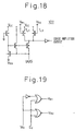
- Figure 18 shows an example of the sense amplifier 107 of the flash memory of Fig. 11.
- the sense amplifier 107 has p-channel type transistors T L 1 and T L 2 serving as load transistors.
- the current supply capacities of these transistors are T L 1 > T L 2 .
- the flash memory has three modes, i.e., an erase verify mode, a normal read mode, and a write verify mode.
- the total capacity of the load transistors for these modes must be the erase verify mode > the normal read mode > the write verify mode.
- Figure 19 shows an example of a logic circuit for providing the control signals V R 1 and V R 2 to the sense amplifier of Fig. 18.
- the logic circuit of Fig. 19 involves a write verify signal WV and an erase verify signal EV. This circuit is advantageous in simplifying the power source of the row decoder when producing the verify voltage.
- the load control logic circuit is applicable for the erase verify operation of the flash memory.
- a semiconductor memory device according to an embodiment of the present invention will be explained with reference to Figs. 20 to 28.
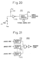
- Figure 20 shows a redundant circuit 210 of a conventional semiconductor memory device related to another embodiment of the present invention.
- the redundant circuit 210 has a fuse 211 serving as defective address specifying means for storing a defective address.
- the fuse 211 is connected or disconnected to provide high (H) or low (L) level.
- a comparator 214 compares the information of the fuse 211 with an external input address, and if they agree with each other, provides an address coincidence signal of, for example, high level H.
- Figure 21 shows a redundant arrangement 2100, which contains a plurality of the conventional redundant circuits of Fig. 20. Outputs of the redundant circuits 210 are passed through a NAND gate and an inverter, to provide a redundancy signal. Only when each input address agrees with the information of the fuse 211 in every redundant circuit 210, is a redundancy signal of high level H provided to read data from redundant cells.
- Figure 22 shows a semiconductor memory device employing the conventional redundant arrangement 2100 of Fig. 21.
- a real cell selector 217 prohibits reading of a real cell 218 (i.e. ordinary cell)
- a redundant cell selector 215 reads a redundant cell 216, thereby replacing a defective real cell with a redundant cell.
- a data read circuit 219 reads data out of a selected one of the redundant cell 216 and real cell 218.
- each fuse (211) requires one address comparator (214).
- address comparator 214
- a corresponding numbers of fuses and address comparators must be prepared. This results in increase in the size and cost of a semiconductor chip.
- the conventional redundant technique has a problem of increasing the size and cost of a semiconductor memory device when the numbers of memory cells and redundant cells increase.
- the above embodiment provides a semiconductor memory device for reducing the size of the semiconductor memory device, to improve the yield of large capacity semiconductor memories and reduce the cost thereof.
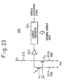
- FIG 23 shows a redundant circuit of a semiconductor memory device in this embodiment.
- This redundant circuit 200 employs a transistor T A , a fuse 201A, a transistor T B , and a fuse 201B in place of the fuse 211 of the conventional redundant circuit 210 of Fig. 20.
- the fuses 201A and 201B are selected according to the logic of an external input address An (/An, an inversion of the address An).
- the address An (/An) is an upper address for selecting one of the blocks of real cells.
- the fuses 201A and 201B of the redundant circuit 200 share an address comparator 204, to reduce the total number of the address comparators 204 and the size and cost of the semiconductor memory device.
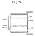
- Figure 24 shows an arrangement of real cells 208 and redundant cells 206 in the semiconductor memory device employing the redundant circuit of Fig. 23.
- the real cells 208 are divided into a first real cell block 208A to be selected with a block selection address An of low level L, and a second real cell block 208B to be selected with a block selection address An of high level H and an inverted address /An of low level L.
- the redundant cells 206 are divided into a first redundant cell block 206A to be replaced with some cells of the first real cell block 208A, and a second redundant cell block 206B to be replaced with some cells of the second real cell block 208B.
- Figure 25 shows a semiconductor memory device employing the redundant circuit of Fig. 23.
- a real cell selector 207 prohibits the reading of a real cell 208
- a redundant cell selector 205 reads a redundant cell 206.
- the semiconductor memory device of Fig. 25 provides an address (a block selection address An) input to the redundant cell selector 205 as well, which selects one of the redundant cells 206A and 206B corresponding to the fuses 201A and 201B of the redundant circuit 200 in response to a logic of the address An.
- the redundant cell selector 205 receives the block address An and selects one of the redundant cells 206A and 206B corresponding to one of the real cell blocks 208A and 208B that is selected according to the block address An.
- a data read circuit 209 reads data out of a selected one of the redundant cell 206 and real cell 208.
- the address comparator 204 is shared by the redundant cell blocks 206A and 206B when replacing a defective real cell with a redundant cell.
- the block selection address An is of one bit for selecting one of the two real cell blocks.
- the block selection address may involve two bits An and An-1 to select one of the four real cell blocks and one of the four redundant cell blocks.
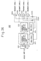
- Figure 26 shows another redundant circuit 200'.
- the redundant circuit 200' includes a cell selector 220, redundant information storing cell arrays 221 and 223, and read circuits 222 and 224.
- the redundant circuit 200' has the two redundant information storing cell arrays 221 and 223 and the two read circuits 222 and 224.
- Each of the redundant information storing cell arrays 221 and 223 includes nonvolatile memory cell transistors such as EPROMs and is used to write data to defective addresses according to external input addresses.
- the cell selector 220 selects one of the cell arrays 221 and 223 according to an address input.
- the read circuits 222 and 224 provide four redundancy signals through AND gates 225A, 225B, 225C, and 225D, and through inverters 226A and 226B.
- This embodiment provides two-bit data from the two cell arrays 221 and 223 in parallel, so that four defective cells can be replaced with redundant cells. It is also possible to provide data of three bits or more in parallel.
- Figure 27 shows still another redundant circuit 200
- Fig. 28 shows a semiconductor memory device employing the redundant circuit of Fig. 27.
- Fig. 27 provides a single bit to replace a plurality of defective real cells 208 with redundant cells 206.
- the redundant circuit 200" reads a single bit according to an address input, and according to a logic of the bit, provides a redundancy signal.
- the redundant circuit 200" provides a redundancy signal to a redundant cell selector 205' and to a real cell selector 207'.
- a part (a real cell block selecting address An) of an address input is also supplied to the selectors 205' and 207', to determine redundant cells to be replaced with defective real cells.
- a semiconductor memory device effectively employs redundant word lines and achieves stable write and verify operations, thereby improving the yield and performance of semiconductor memories.
- the semiconductor memory device can also replace defective real cells with redundant cells without increasing the size of a semiconductor memory device, thereby improving the yield of large capacity semiconductor memories and reducing the cost thereof.
Abstract
Description
- The present invention relates to a semiconductor memory device, and more particularly, to a flash memory, i.e., a nonvolatile semiconductor memory device having electrically and collectively erasable characteristics.
- Recently, in accordance with popularization of computers, word processors, and the like, a plurality of semiconductor memory devices, typically non-volatile semiconductor memory devices, e.g., flash memory, used in such information processors, have been developed and produced.
- The flash memory, which is one kind of nonvolatile semiconductor memory device, can be made programmable by the user. Further, the flash memory can be rewritten by electrically and collectively erasing the stored data, and then by programming. Therefore, the flash memories have attracted considerable attention as a replacement for magnetic storage devices because they are suitable for integration. Note, there is a necessity of improving redundant circuits, write circuits, and overerasing preventive measures for such a flash memory.
- EP A 0 239 196 discloses a semiconductor device having a regular memory cell array and a redundancy memory cell array each provided with a plurality of word lines and bit lines. Memory cells are arranged at each intersection of the word lines and bit lines. A first selection means selects a word or bit line belonging to the regular memory cell array in accordance with upper and lower address bits and a second selection means selects a word or bit line belonging to the redundancy memory cell array in accordance with lower address bits. A control means compares each input upper address with each programmed upper address and controls the first and second selection means so that the selection of the word or bit line belonging to the regular memory cell array is not selected and a word or bit line belonging to the redundancy memory cell array is selected instead, whenever each upper address bit coincides with each of the programmed upper address bits.
- The present invention may provide a semiconductor memory device for realizing effective word line redundancy and stable write and verify operations in a semiconductor memory device, to improve the yield and performance of the semiconductor memory device.
- The present invention may also provide a semiconductor memory device of reduced size, to improve the yield of large capacity semiconductor memories and reduce the cost thereof.
- According to the present invention, there is provided a semiconductor memory device having: 2n word lines; a plurality of bit lines; a plurality of nonvolatile memory cells each formed of a MIS transistor disposed at each intersection of said word lines and said bit lines, a threshold voltage of said MIS transistor being externally electrically controllable; a write circuit for writing data to a memory cell located at an intersection of selected ones of said word lines and said bit lines; a sense amplifier for reading data out of said memory cells; a first means for simultaneously selecting a block of 2m (n>m) word lines among said 2n word lines; and a second means for not selecting a block of 2k (m>k) word lines among said 2m word lines, said second means not selecting said block of 2k word lines and selecting a block of 2k word lines prepared outside said 2n word lines when any one of said 2k word lines among said 2m word lines is defective; where n, m, k are integers; characterised in that: said block of 2n word lines forms a real cell block, said block of 2m word lines forms an erase block, and said block of 2k word lines outside said block of 2n word lines forms a redundant cell block.
- The selected word lines may receive a negative voltage, and the unselected word lines may receive a zero or positive voltage.
- The semiconductor memory device may comprise a plurality of real cell blocks, a plurality of defective address specifying units for specifying defective addresses of the respective real cell blocks, and an address comparing unit shared by the defective address specifying unit, for comparing the defective addresses with addresses in the real cell blocks.
- The semiconductor memory device may also comprise a redundant information storing cell array for writing data to a defective address according to an externally provided address, a cell selection circuit for selecting the redundant information storing cell array according to the externally provided address, and a read circuit for reading an output of the redundant information storing cell array selected by the cell selection circuit, and providing a redundancy signal.
- The present invention will be more clearly understood from the description of the preferred embodiments as set forth below with reference to the accompanying drawings, wherein:
- Figure 1 is diagram for explaining the operation of a memory cell used for a semiconductor memory device related to the present invention;
- Figure 2 is a block diagram showing a conventional semiconductor memory device related to the present invention;
- Figure 3 is a circuit diagram showing a column address buffer of the semiconductor memory device of Fig. 2;
- Figure 4 is a circuit diagram showing a row address buffer of the semiconductor memory device of Fig. 2;
- Figure 5 is a circuit diagram showing a row decoder of the semiconductor memory device of Fig. 2;
- Figure 6 is a circuit diagram showing a column decoder of the semiconductor memory device of Fig. 2;
- Figure 7 is a circuit diagram showing a write circuit of the semiconductor memory device of Fig. 2;
- Figure 8 is a circuit diagram showing a source voltage supply circuit of the semiconductor memory device of Fig. 2;
- Figure 9 is a circuit diagram showing a sense amplifier of the semiconductor memory device of Fig. 2;
- Figure 10 is a diagram showing an example of write characteristics curves of the semiconductor memory device of Fig. 2;
- Figure 11 is a circuit block diagram showing an embodiment of a semiconductor memory device according to the present invention;.
- Figure 12 is a circuit diagram showing a row address buffer of the semiconductor memory device of Fig. 11;
- Figure 13 is a circuit diagram showing a row decoder of the semiconductor memory device of Fig. 11;
- Figure 14 is a circuit diagram showing a coincidence circuit of the semiconductor memory device of Fig. 11;
- Figure 15 is a circuit diagram showing an essential part of a row decoder of the semiconductor memory device of Fig. 11;
- Figure 16 is a diagram showing a waveform of a signal applied to the circuit of Fig. 15;
- Figure 17 is a circuit diagram showing a verify voltage generator of the semiconductor memory device of Fig. 11;
- Figure 18 is a circuit diagram showing a sense amplifier of the semiconductor memory device of Fig. 11;
- Figure 19 is a circuit diagram showing a logic circuit for producing a control signal to the sense amplifier of Fig. 18;
- Figure 20 is a circuit block diagram showing a redundant circuit of a conventional semiconductor memory device related to another embodiment of the present invention;
- Figure 21 is a circuit block diagram showing an arrangement of the conventional redundant circuits of Fig. 20;
- Figure 22 is a block diagram showing a semiconductor memory device employing the conventional redundant circuit of Fig. 20;
- Figure 23 is a circuit block diagram showing an embodiment of a redundant circuit for the semiconductor memory device of Fig. 20;
- Figure 24 is a diagram showing real cells and redundant cells of a semiconductor memory device employing the redundant circuit of Fig. 23;
- Figure 25 is a block diagram showing a semiconductor memory device employing the redundant circuit of Fig. 23;
- Figure 26 is a circuit block diagram showing another embodiment of a redundant circuit for the semiconductor memory device;
- Figure 27 is a circuit block diagram showing still another embodiment of a redundant circuit for the semiconductor memory device; and
- Figure 28 is a block diagram showing a semiconductor memory device employing the redundant circuit of Fig. 27.
-
- For a better understanding of the preferred embodiments, the problems of the related art will be explained, with reference to Figs. 1 to 10.
- Figure 1 shows a memory cell (MC) of an electrically collectively erasable nonvolatile semiconductor memory device (a flash memory) to which the present invention is applied. The memory cell (cell transistor) MC has a floating gate FG. The floating gate FG is located between a source and a drain and is insulated from other regions. A control gate CG is formed above the floating gate FG.
- To write data to the cell transistor MC, a drain voltage Vd applied to a drain DD is substantially equalized with a power source voltage Vcc. A gate voltage Vg applied to the control. gate CG is a positive high voltage (about +10 volts at the maximum). A source voltage Vs applied to a source SS is zero. Electrons are injected from the drain DD to the floating gate FG, to write data "0" to the cell transistor MC. The drain voltage Vd may be a write voltage Vpp, if the voltage Vpp is available. The high gate voltage Vg may be the write voltage Vpp, or may be produced by increasing the power source voltage Vcc.
- To erase data from the cell transistor MC, the gate voltage Vg is set to a high negative value (about -10 volts at the lowest). The drain voltage Vd is opened to put the drain DD in a floating state. The source voltage Vs is equalized with the power source voltage Vcc. Electrons are pulled from the floating gate FG to the source SS, to erase data from the cell transistor MC, i.e., to write data "1" to the cell transistor. To read data from the cell transistor MC, the gate voltage Vg is equalized to the power source voltage Vcc, the drain voltage Vd to about one volt, and the source voltage Vs to zero. Then, it is checked to see whether or not a drain current flows, to determine if the data stored in the cell transistor MC is "1" or "0".
- Figure 2 shows a conventional semiconductor memory device related to the present invention. This semiconductor memory device has a
row address buffer 111, arow decoder 112, acolumn address buffer 113, acolumn decoder 114, a data I/O buffer 115, awrite circuit 116, asense amplifier 117, anegative voltage generator 118, and a sourcevoltage supply circuit 119. The semiconductor memory device involves bit lines BLs, word lines WLs, a write control signal W that will be high level H when writing data, and an erase control signal E that will be high level H when erasing data. - When reading data from a memory cell (cell transistor) MC, a row address is given to select a word line WL, and a column address to select a bit line BL, thereby selecting the memory cell. The
sense amplifier 117 senses whether or not a current flows through the selected memory cell, to determine whether data stored in the cell is "1" or "0". - When writing data to a memory cell MC, the write control signal W is set to high level H. The
write circuit 116 provides a bus BUS with a write voltage, and thecolumn decoder 114 connects the bus BUS to a given bit line BL. Therow decoder 112 applies the write voltage to a selected word line WL. When erasing data from memory cells MCs, the erase control signal E is set to high level H. The sourcevoltage supply circuit 119 applies an erase voltage to source lines of the memory cells MCs, and thecolumn address buffer 113 puts the bit lines BLs in an unselected state. Therow address buffer 111 simultaneously selects a given number of word lines WLs, and therow decoder 112 sets the selected word lines WLs to low level L and the unselected word lines WLs to high level H. Thenegative voltage generator 118 applies a negative voltage to the word lines WLs of low level L. - Figures 3 to 6 show examples of the
column address buffer 113,row address buffer 111,row decoder 112,column decoder 114 of the semiconductor memory device of Fig. 2, respectively. - When reading data from a memory cell MC, the erase control signal E is at low level L. The
column address buffer 113 of Fig. 3 androw address buffer 111 of Fig. 4 provide positive and negative logic values with respect to an input address. Therow decoder 112 of Fig. 5 involves a signal that oscillates at a given frequency when erasing or writing data, and a signal R that is at high level H for some period of time after the reception of the input address. - When reading data, the write control signal W is at low level L. Transistors T1 and T2 of the
row decoder 112 of Fig. 5 introduce the power source voltage Vcc. According to an address input (an output of the row address buffer 111), a predetermined decoder is selected. For example, a node N3 of Fig. 5 becomes high level H. If the signal R provides a pulse of high level H in this state, nodes N2 and N4 are reset to zero. When the signal R restores low level L, the node N2 is charged to the power source voltage Vcc. Due to the self-bootstrap effect of transistors T6 and T7, the node N4 is also charged to the level of the power source voltage Vcc. Thecolumn decoder 114 operates similarly to therow decoder 112. As a result, the power source voltage Vcc is applied to a predetermined word line WL, and a predetermined bit line BL is connected to thesense amplifier 117. - Figures 7 and 8 show examples of the
write circuit 116 and sourcevoltage supply circuit 119 of the semiconductor memory device of Fig. 2, respectively. - With the write control signal W of high level H, data of low level L, and an inverted data signal /DATA of high level H, the
write circuit 116 of Fig. 7 increases the power source voltage Vcc to provide the bus BUS with a high voltage. With this high voltage, data is written to a given cell transistor. The signal /DATA is transferred as a write signal from the data I/O buffer 115 to thewrite circuit 116. Note, a mark "/" denotes an inverted level or inverted signal, and thus, for example, the signal /DATA denotes an inverted level of signal DATA. - When erasing data, the erase control signal E is raised to high level H. In the
column address buffer 113 of Fig. 3, both outputs A and /A are set to low level L. These outputs A and /A are applied to thecolumn decoder 114 to put the columns (bit lines BLs) in an unselected state. Namely, the bit lines BLs are electrically disconnected from every node. In therow address buffer 111, the erase control signal E is applied to "m" buffer elements among "n" buffer elements in total. As a result, therow decoder 112 of Fig. 5 simultaneously selects 2m word lines. In therow decoder 112, the erase control signal E is at high level H, so that the node N2 receives zero volts and the node N5 receives high level H. As a result, the selected word lines WLs are set to low level L, and the unselected word lines WLs are set to high level H. - The
negative voltage generator 118 provides an erase voltage to the word lines WLs of low level L. The word lines WLs at high level H are maintained at high level H because the potential of an output N6 of a NOR gate of Fig. 5 is always at low level L, and therefore, the signal is not transmitted to a capacitance element connected to the node N6. At this time, the sourcevoltage supply circuit 119 of Fig. 8 applies the power source voltage Vcc to the source SS of each cell transistor MC. As a result, the cell transistors of the 2m word lines are simultaneously erased. - Figure 9 shows an example of the
sense amplifier 117 of the semiconductor memory device of Fig. 2. - An output of the
sense amplifier 117 of Fig. 9 will be high level H or low level L depending on whether or not the drain current of a selected cell transistor MC is larger than the allowable current of a transistor T8. Transistors T9 , T10 , T11 , and T12 form a bias circuit that sets the potential of the bus BUS to about one volt. - When writing data, the write control signal W is set to high level H, and the signal is oscillated at a predetermined frequency. The transistors T4 and T5 provide the node N1 with a write voltage. Similar to the read operation with the signal R, a pulse of high level H is applied to charge the node N2 to the write voltage. The node N4 is also charged to the same level as the node N2 due to the self-bootstrap effect of the transistors T6 and T7. The
column decoder 114 operates in the same manner. Consequently, the write voltage is supplied to a selected word line WL, and a selected bit line BL is connected to thewrite circuit 116. - As explained with reference to Figs. 2 to 9, the semiconductor memory device (flash memory) of the related art collectively erases a block containing a large number of memory cells, e.g., 512 kilobits. If this large block includes a defective cell, the block as a whole must be replaced with a block containing a large number of redundant memory cells. This sort of replacement deteriorates the efficiency of redundancy. Namely, it is difficult for the related art to replace many defective cells with a small number of redundant cells. If the memory cell MC11 of Fig. 1 is overerased, a current will always flow to the bit line BL1 through the memory cell MC11, to hinder correct read and write operations.
- Figure 10 shows the write characteristics of a semiconductor memory device (a flash memory).
- The related art mentioned above provides a write drain voltage by increasing the power source voltage Vcc. Meanwhile, the bit line driving capacity of the
write circuit 116 is limited, so that the potential of a bit line decreases when a large current is supplied to the bit line. When an overerased cell transistor is present, the write characteristic curve of the overerased cell transistor may cross a load curve of thewrite circuit 116 in a write impossible region A, as indicated with continuous lines in Fig. 10. If this happens, a write operation will be disabled. The write operation is enabled only between points D and B. A word line voltage for an erase or write verify operation is usually provided by dropping the external write voltage. Since the related art employs no external write voltage, it is difficult for the related art to carry out the verify operation. If some cell transistors are overerased, it is difficult to restore normal operation by replacing the overerased cell transistors with spare cell transistors. Namely, the normal operation will never resume by replacing word lines containing the overerased cells with redundant word lines. In this case, the overerased cells may be rewritten to cancel the overerased state and restore the normal operation. The overerased cells, however, pass a larger current around a point A of Fig. 10 to make such writing difficult. - A semiconductor memory device according to the present invention will be explained with reference to Figs. 11 to 19.
- Figure 11 shows the semiconductor memory device (flash memory) according to the present invention. This memory differs from the conventional semiconductor memory device of Fig. 2 in that it additionally has a
coincidence circuit 120 for comparing an input address with a defective address, and aredundant row decoder 130. Arow address buffer 101, arow decoder 102, acolumn address buffer 103, acolumn decoder 104, a data I/O buffer 105, awrite circuit 106, asense amplifier 107, anegative voltage generator 108, and a sourcevoltage supply circuit 109 of this embodiment correspond to therow address buffer 111,row decoder 112,column address buffer 113,column decoder 114, data I/O buffer 115, writecircuit 116,sense amplifier 117,negative voltage generator 118, and sourcevoltage supply circuit 119 of the related art of Fig. 2. - The operation of the embodiment will now be explained. When writing or reading data to or from a memory cell (cell transistor) of the semiconductor memory device, the
coincidence circuit 120 compares an input address with each defective address stored therein. If they agree with each other, thecoincidence circuit 120 provides therow address buffer 101 andredundant row decoder 130 with an output signal to put therow decoder 102 in an unselected state and theredundant row decoder 130 in a selected state. This enables a redundant cell to be accessed instead of a defective cell. When erasing data from the semiconductor memory device, an erase control signal E of high level H is provided to thecolumn address buffer 103,row address buffer 101,row decoder 102,coincidence circuit 120, andredundant row decoder 130. - If there is no defective cell (transistor) in a memory cell array, i.e., if the redundancy is not used, a normal erase operation is carried out as previously explained. A redundancy control signal RED from the
coincidence circuit 120 indicates no redundancy. - If there is a defective cell, the
coincidence circuit 120 stores the address of the defective cell. In this embodiment, there are 2n word lines in total, and 2m word lines among the 2n word lines form an erase block. The embodiment employs 2k redundant (spare) word lines. To write or read data, the number of bits of defective address storage elements in thecoincidence circuit 120 must be "n-k." Since an erase block includes 2m word lines, the number of address bits necessary for selecting the erase block is "n-m." When erasing data, "n-m" addresses are provided to select a block of 2m word lines. The input addresses are compared with upper "n-m" address bits among the "n-k" address bits stored in thecoincidence circuit 120. If they agree with each other, it is determined that the erase block of 2k word lines includes a defective cell. - Address information representing the block of 2k word lines including the defective cell among the block of 2m word lines is given by the remaining "m-k" address bits stored in the
coincidence circuit 120. Consequently, therow decoder 102 sets the block of 2k word lines specified with the "m-k" address bits among the block of 2m word lines to be unselected. When the coincidence of "n-m" address bits is found in erasing 2m word lines, theredundant row decoder 130 is activated to erase the 2k redundant word lines. - Figures 12 to 14 show essential parts of the
row address buffer 101,row decoder 102, andcoincidence circuit 120 of the semiconductor memory device of Fig. 11. - In Fig. 12, there are "n" buffers in the
row address buffer 101. Lower "m" buffers receive the erase control signal E to select 2m word lines in an erase operation. Any one of the m buffers receives the redundancy control signal RED. If this signal is high level H in a write or read operation, it means that an input address agrees with a defective address, and therefore, the word line WL is set to be unselected. - The redundancy control signal RED is an output signal of the
coincidence circuit 120 of Fig. 14. Thecoincidence circuit 120 includes address storage fuses used to specify a block of 2k word lines among the 2n word lines, and a fuse RUSE used to store the state of use of redundancy. Since the erase control signal E is at low level L except in an erase operation, the redundancy control signal RED becomes high level H only when all pieces of fuse information agree with input information pieces. In the erase operation, the redundancy control signal RED becomes high level H if upper "n-m" addresses ARBm+1 to ARBn coincide with input addresses. Fuse data of "m-k" addresses ARBk+1 to ARBm are provided directly to a NAND gate of Fig. 13. As a result, a block of 2k word lines among a block of 2m word lines is set to be unselected. The redundancy control signal RED is also provided to theredundant row decoder 130. In this way, an optional block of 2k word lines in an erase block of 2m word lines is replaceable with a block of redundant (spare) word lines. - If a memory cell is overerased in the semiconductor memory device (flash memory), it deteriorates the yield. The bit lines of the semiconductor memory device are shared by the redundant cells and real cells, and therefore, it is impossible to save the overerased cell by replacing it with the redundant cell. For example, if a memory cell (cell transistor) MC11 is overerased in Fig. 11, the cell MC11 may be replaced with a redundant cell MCR11. In this case, however, the overerased cell MC11 passes current even when a word line WL1 is at low level L. If this happens, data "0" of a cell existing on the bit line BL1 will not be correctly read. This problem is easily solved by writing data "0" in the overerased cell MC11 before replacing it with the redundant cell MCR11. Namely, electrons are injected into the floating gate of the cell MC11 before replacing it with the redundant cell.
- The overerasing of a memory cell will be explained with reference to Fig. 10, which shows the write characteristics curve of a semiconductor memory device. The floating gate of an overerased cell is positively charged to increase a current at a point A on the curve, thus disabling data write. To solve this problem, it is necessary to control the gate level of any cell when writing data to the cell, such that a current flowing through the cell does not exceed the load curve of the
write circuit 106 around the point A. This is easily achieved by continuously providing pulses to a corresponding word line WL during the data write. When the word line WL receives the pulses, it surely realizes a curve C indicated with a dotted line in Fig. 10 when moving from low level L to high level H, or from high level H to low level L. Consequently, the data write is enabled irrespective of the condition of the floating gate. - Figure 15 shows an essential part of an example of the
row decoder 102 of the semiconductor memory device of Fig. 11, and corresponds to the input portion B of therow decoder 112 of the conventional semiconductor memory device of Fig. 5. A NOR gate of Fig. 15 receives a signal W whose waveform is shown in Fig. 16. With this signal, the potential of the node N2 of Fig. 5 is continuously oscillated between zero and a write potential, to continuously provide pulses to a word line WL. Instead of applying the pulses, it is possible to employ a circuit for applying an intermediate voltage to a word line. Generally, a write or erase operation of a semiconductor memory device is followed by a verify operation, which is achieved by applying a verify voltage to read data from a word line. The verify voltage must be constant irrespective of changes in environmental conditions of the semiconductor memory device such as a change in a power source voltage. Accordingly, it is practical to provide the verify voltage by increasing a reference potential (Vss) of the semiconductor memory device. - Figure 17 shows an example of a verify
voltage generator 150 of the semiconductor memory device of Fig. 11. This circuit generates a verify voltage applied to the node N1 of the row decoder circuit 112 (102) of Fig. 5. - The verify
voltage generator 150 of Fig. 17 includes aclamp circuit 151, anoscillator 152, and a step-upcircuit 153. Theclamp circuit 151 has transistors T13 and T14 for determining a clamp voltage. These transistors are p-channel type and n-channel type MOS (MIS) transistors connected in series as diodes. According to a CMOS process, the channel regions of transistors are simultaneously fabricated to cancel fluctuations in the thresholds of the transistors. This results in stabilizing the clamp voltage. - An n-channel type MOS transistor T1 5 has a threshold of about zero volts. This transistor provides the
oscillator 152 with the clamp voltage. The step-upcircuit 153 operates according to a low power source voltage (ground voltage) Vss. A verify voltage at the node N1, therefore, is stable regardless of the power source voltage. Erase and write verify operations are carried out with different voltages. Different clamp voltages are easily produced by changing the number of transistors (T13 , T14 , ...) of theclamp circuit 151. A signal VR becomes high level H when carrying out the verify operation. The verify operation may be carried out by changing a decision current of the sense amplifier. - Figure 18 shows an example of the
sense amplifier 107 of the flash memory of Fig. 11. Thesense amplifier 107 has p-channel type transistors TL1 and TL2 serving as load transistors. The current supply capacities of these transistors are TL1 > TL2 . The flash memory has three modes, i.e., an erase verify mode, a normal read mode, and a write verify mode. The total capacity of the load transistors for these modes must be the erase verify mode > the normal read mode > the write verify mode. The circuit of Fig. 18 realizes this relationship with VR1 =VR2 =L for the erase verify mode, VR1 =L and VR2 =H for the normal read mode, and VR1 =H and VR2 =L for the write verify mode. - Figure 19 shows an example of a logic circuit for providing the control signals VR1 and VR2 to the sense amplifier of Fig. 18. The logic circuit of Fig. 19 involves a write verify signal WV and an erase verify signal EV. This circuit is advantageous in simplifying the power source of the row decoder when producing the verify voltage. The load control logic circuit is applicable for the erase verify operation of the flash memory.
- A semiconductor memory device according to an embodiment of the present invention will be explained with reference to Figs. 20 to 28.
- Figure 20 shows a
redundant circuit 210 of a conventional semiconductor memory device related to another embodiment of the present invention. Theredundant circuit 210 has afuse 211 serving as defective address specifying means for storing a defective address. Thefuse 211 is connected or disconnected to provide high (H) or low (L) level. Acomparator 214 compares the information of thefuse 211 with an external input address, and if they agree with each other, provides an address coincidence signal of, for example, high level H. - Figure 21 shows a
redundant arrangement 2100, which contains a plurality of the conventional redundant circuits of Fig. 20. Outputs of theredundant circuits 210 are passed through a NAND gate and an inverter, to provide a redundancy signal. Only when each input address agrees with the information of thefuse 211 in everyredundant circuit 210, is a redundancy signal of high level H provided to read data from redundant cells. - Figure 22 shows a semiconductor memory device employing the conventional
redundant arrangement 2100 of Fig. 21. When theredundant arrangement 2100 provides a redundancy signal, areal cell selector 217 prohibits reading of a real cell 218 (i.e. ordinary cell), and aredundant cell selector 215 reads aredundant cell 216, thereby replacing a defective real cell with a redundant cell. A data readcircuit 219 reads data out of a selected one of theredundant cell 216 andreal cell 218. - According to the prior art of Figs. 20 to 22, each fuse (211) requires one address comparator (214). When many defective memory cells must be replaced with redundant cells, a corresponding numbers of fuses and address comparators must be prepared. This results in increase in the size and cost of a semiconductor chip.
- In this way, the conventional redundant technique has a problem of increasing the size and cost of a semiconductor memory device when the numbers of memory cells and redundant cells increase.
- The above embodiment provides a semiconductor memory device for reducing the size of the semiconductor memory device, to improve the yield of large capacity semiconductor memories and reduce the cost thereof.
- Figure 23 shows a redundant circuit of a semiconductor memory device in this embodiment. This
redundant circuit 200 employs a transistor TA, afuse 201A, a transistor TB, and afuse 201B in place of thefuse 211 of the conventionalredundant circuit 210 of Fig. 20. Thefuses fuses redundant circuit 200 share anaddress comparator 204, to reduce the total number of theaddress comparators 204 and the size and cost of the semiconductor memory device. - Figure 24 shows an arrangement of
real cells 208 andredundant cells 206 in the semiconductor memory device employing the redundant circuit of Fig. 23. Thereal cells 208 are divided into a firstreal cell block 208A to be selected with a block selection address An of low level L, and a secondreal cell block 208B to be selected with a block selection address An of high level H and an inverted address /An of low level L. Theredundant cells 206 are divided into a firstredundant cell block 206A to be replaced with some cells of the firstreal cell block 208A, and a secondredundant cell block 206B to be replaced with some cells of the secondreal cell block 208B. When an address (An-1, An-2, ..., etc) that is common for thereal cell blocks - Figure 25 shows a semiconductor memory device employing the redundant circuit of Fig. 23. When the
redundant circuit 200 provides a redundancy signal, areal cell selector 207 prohibits the reading of areal cell 208, and aredundant cell selector 205 reads aredundant cell 206. Unlike the semiconductor memory device of Fig. 22, the semiconductor memory device of Fig. 25 provides an address (a block selection address An) input to theredundant cell selector 205 as well, which selects one of theredundant cells fuses redundant circuit 200 in response to a logic of the address An. Namely, theredundant cell selector 205 receives the block address An and selects one of theredundant cells real cell blocks circuit 209 reads data out of a selected one of theredundant cell 206 andreal cell 208. - As explained above, the
address comparator 204 is shared by theredundant cell blocks - Figure 26 shows another redundant circuit 200'. The redundant circuit 200' includes a
cell selector 220, redundant information storingcell arrays circuits - The redundant circuit 200' has the two redundant information storing
cell arrays circuits - Each of the redundant information storing
cell arrays cell selector 220 selects one of thecell arrays circuits gates inverters cell arrays - Figure 27 shows still another
redundant circuit 200", and Fig. 28 shows a semiconductor memory device employing the redundant circuit of Fig. 27. - Unlike the redundant circuit 200' of Fig. 26 that provides a plurality of bits (two bits) in parallel, the embodiment of Fig. 27 provides a single bit to replace a plurality of defective
real cells 208 withredundant cells 206. - The
redundant circuit 200" reads a single bit according to an address input, and according to a logic of the bit, provides a redundancy signal. In the semiconductor memory device of Fig. 28, theredundant circuit 200" provides a redundancy signal to a redundant cell selector 205' and to a real cell selector 207'. A part (a real cell block selecting address An) of an address input is also supplied to the selectors 205' and 207', to determine redundant cells to be replaced with defective real cells. - As explained above, a semiconductor memory device according to the present invention effectively employs redundant word lines and achieves stable write and verify operations, thereby improving the yield and performance of semiconductor memories.
- The semiconductor memory device can also replace defective real cells with redundant cells without increasing the size of a semiconductor memory device, thereby improving the yield of large capacity semiconductor memories and reducing the cost thereof.
- Many different embodiments of the present invention may be constructed without departing from the scope of the present invention, and it should be understood that the present invention is not limited to the specific embodiments described in this specification, except as defined in the appended claims.
Claims (7)
- A semiconductor memory device having:characterised in that:2n word lines (WLs);a plurality of bit lines (BLs);a plurality of nonvolatile memory cells (MCs) each formed of a MIS transistor disposed at each intersection of said word lines and said bit lines, a threshold voltage of said MIS transistor being externally electrically controllable;a write circuit (106) for writing data to a memory cell located at an intersection of selected ones of said word lines and said bit lines;a sense amplifier (107) for reading data out of said memory cells;a first means (101, 102, 120) for simultaneously selecting a block of 2m (n>m) word lines among said 2n word lines; anda second means (101, 102, 120, 130) for not selecting a block of 2k (m>k) word lines among said 2m word lines, said second means (101, 102, 120, 130) not selecting said block of 2k word lines and selecting a block of 2k word lines prepared outside said 2n word lines when any one of said 2k word lines among said 2m word lines is defective; where n, m, k are integers;
said block of 2n word lines forms a real cell block, said block of 2m word lines forms an erase block, and said block of 2k word lines outside said block of 2n word lines forms a redundant cell block. - A semiconductor memory device as claimed in claim 1, wherein in use, said selected word lines receive a negative voltage, and said unselected word lines receive a zero or positive voltage.
- A semiconductor memory device as claimed in claims 1 or 2 wherein a plurality of real cell blocks are provided and wherein the device further comprises:a plurality of defective address specifying means (201A, TA, 201B, TB) for specifying defective addresses of said respective real cell blocks; andan address comparing means (204) shared by said defective address specifying means, for comparing said defective addresses with addresses in said real cell blocks.
- A semiconductor memory device as claimed in claim 3, wherein said semiconductor memory device further comprises:a redundant circuit (200) having said defective address specifying means and said address comparing means;a real cell selecting means (207) for receiving an output of said redundant circuit and a block address for specifying one of said real cell blocks, and controlling the selection and non-selection of memory cells in said specified real cell block; anda redundant cell selecting means (205) for receiving the output of said redundant circuit and said block address, and controlling the selection and non-selection of said redundant cells.
- A semiconductor memory device according to any preceding claim, further comprising:a redundant information storing cell array (221; 221, 223) for writing data to a defective address according to an externally provided address;a cell selection circuit (220) for selecting said redundant information storing cell array according to the externally provided address; anda read circuit (222, 224) for reading an output of said redundant information storing cell array selected by said cell selection circuit, and providing a redundancy signal.
- A semiconductor memory device as claimed in claim 5, wherein said redundant information storing cell array and said read circuit are provided in plural, outputs of said read circuits are logically processed, and thereby a plurality of redundancy signals are output.
- A semiconductor memory device as claimed in claim 5 or 6, wherein said redundant information storing cell array is constituted by a plurality of nonvolatile memory cell transistors.
Priority Applications (8)
| Application Number | Priority Date | Filing Date | Title |
|---|---|---|---|
| EP01109448A EP1158530B1 (en) | 1992-12-03 | 1993-06-25 | Nonvolatile semiconductor memory device having electrically and collectively erasable characteristics |
| EP01109453A EP1158532B1 (en) | 1992-12-03 | 1993-06-25 | Semiconductor memory device |
| EP01109449A EP1158536B1 (en) | 1992-12-03 | 1993-06-25 | Semiconductor memory device |
| EP01109451A EP1118937B1 (en) | 1992-12-03 | 1993-06-25 | Nonvolatile semiconductor memory device having electrically and collectively erasable characteristics |
| EP01109454A EP1158534B1 (en) | 1992-12-03 | 1993-06-25 | Semiconductor memory device |
| EP01109455A EP1158535A3 (en) | 1992-12-03 | 1993-06-25 | Nonvolatile semiconductor memory device having electrically and collectively erasable characteristics |
| EP01109450A EP1158531B1 (en) | 1992-12-03 | 1993-06-25 | Semiconductor memory device |
| EP01109452A EP1158526B1 (en) | 1992-12-03 | 1993-06-25 | Nonvolatile semiconductor memory device having electrically and collectively erasable characteristics |
Applications Claiming Priority (9)
| Application Number | Priority Date | Filing Date | Title |
|---|---|---|---|
| JP32428492 | 1992-12-03 | ||
| JP324284/92 | 1992-12-03 | ||
| JP32428492A JP3347374B2 (en) | 1992-12-03 | 1992-12-03 | Decoder circuit and semiconductor memory device |
| JP34948192 | 1992-12-28 | ||
| JP34948192A JP3159816B2 (en) | 1992-12-28 | 1992-12-28 | Nonvolatile semiconductor memory device |
| JP349481/92 | 1992-12-28 | ||
| JP00030493A JP3392165B2 (en) | 1993-01-05 | 1993-01-05 | Semiconductor storage device |
| JP30493 | 1993-01-05 | ||
| JP304/93 | 1993-01-05 |
Related Child Applications (8)
| Application Number | Title | Priority Date | Filing Date |
|---|---|---|---|
| EP01109454A Division EP1158534B1 (en) | 1992-12-03 | 1993-06-25 | Semiconductor memory device |
| EP01109452A Division EP1158526B1 (en) | 1992-12-03 | 1993-06-25 | Nonvolatile semiconductor memory device having electrically and collectively erasable characteristics |
| EP01109453A Division EP1158532B1 (en) | 1992-12-03 | 1993-06-25 | Semiconductor memory device |
| EP01109449A Division EP1158536B1 (en) | 1992-12-03 | 1993-06-25 | Semiconductor memory device |
| EP01109450A Division EP1158531B1 (en) | 1992-12-03 | 1993-06-25 | Semiconductor memory device |
| EP01109451A Division EP1118937B1 (en) | 1992-12-03 | 1993-06-25 | Nonvolatile semiconductor memory device having electrically and collectively erasable characteristics |
| EP01109455A Division EP1158535A3 (en) | 1992-12-03 | 1993-06-25 | Nonvolatile semiconductor memory device having electrically and collectively erasable characteristics |
| EP01109448A Division EP1158530B1 (en) | 1992-12-03 | 1993-06-25 | Nonvolatile semiconductor memory device having electrically and collectively erasable characteristics |
Publications (3)
| Publication Number | Publication Date |
|---|---|
| EP0600151A2 EP0600151A2 (en) | 1994-06-08 |
| EP0600151A3 EP0600151A3 (en) | 1998-11-11 |
| EP0600151B1 true EP0600151B1 (en) | 2001-11-07 |
Family
ID=27274405
Family Applications (9)
| Application Number | Title | Priority Date | Filing Date |
|---|---|---|---|
| EP01109453A Expired - Lifetime EP1158532B1 (en) | 1992-12-03 | 1993-06-25 | Semiconductor memory device |
| EP01109449A Expired - Lifetime EP1158536B1 (en) | 1992-12-03 | 1993-06-25 | Semiconductor memory device |
| EP01109450A Expired - Lifetime EP1158531B1 (en) | 1992-12-03 | 1993-06-25 | Semiconductor memory device |
| EP01109455A Withdrawn EP1158535A3 (en) | 1992-12-03 | 1993-06-25 | Nonvolatile semiconductor memory device having electrically and collectively erasable characteristics |
| EP01109448A Expired - Lifetime EP1158530B1 (en) | 1992-12-03 | 1993-06-25 | Nonvolatile semiconductor memory device having electrically and collectively erasable characteristics |
| EP93110192A Expired - Lifetime EP0600151B1 (en) | 1992-12-03 | 1993-06-25 | Nonvolatile semiconductor memory device having electrically and collectively erasable characteristics |
| EP01109451A Expired - Lifetime EP1118937B1 (en) | 1992-12-03 | 1993-06-25 | Nonvolatile semiconductor memory device having electrically and collectively erasable characteristics |
| EP01109454A Expired - Lifetime EP1158534B1 (en) | 1992-12-03 | 1993-06-25 | Semiconductor memory device |
| EP01109452A Expired - Lifetime EP1158526B1 (en) | 1992-12-03 | 1993-06-25 | Nonvolatile semiconductor memory device having electrically and collectively erasable characteristics |
Family Applications Before (5)
| Application Number | Title | Priority Date | Filing Date |
|---|---|---|---|
| EP01109453A Expired - Lifetime EP1158532B1 (en) | 1992-12-03 | 1993-06-25 | Semiconductor memory device |
| EP01109449A Expired - Lifetime EP1158536B1 (en) | 1992-12-03 | 1993-06-25 | Semiconductor memory device |
| EP01109450A Expired - Lifetime EP1158531B1 (en) | 1992-12-03 | 1993-06-25 | Semiconductor memory device |
| EP01109455A Withdrawn EP1158535A3 (en) | 1992-12-03 | 1993-06-25 | Nonvolatile semiconductor memory device having electrically and collectively erasable characteristics |
| EP01109448A Expired - Lifetime EP1158530B1 (en) | 1992-12-03 | 1993-06-25 | Nonvolatile semiconductor memory device having electrically and collectively erasable characteristics |
Family Applications After (3)
| Application Number | Title | Priority Date | Filing Date |
|---|---|---|---|
| EP01109451A Expired - Lifetime EP1118937B1 (en) | 1992-12-03 | 1993-06-25 | Nonvolatile semiconductor memory device having electrically and collectively erasable characteristics |
| EP01109454A Expired - Lifetime EP1158534B1 (en) | 1992-12-03 | 1993-06-25 | Semiconductor memory device |
| EP01109452A Expired - Lifetime EP1158526B1 (en) | 1992-12-03 | 1993-06-25 | Nonvolatile semiconductor memory device having electrically and collectively erasable characteristics |
Country Status (4)
| Country | Link |
|---|---|
| US (10) | US5452251A (en) |
| EP (9) | EP1158532B1 (en) |
| KR (1) | KR960007638B1 (en) |
| DE (8) | DE69333263T2 (en) |
Families Citing this family (103)
| Publication number | Priority date | Publication date | Assignee | Title |
|---|---|---|---|---|
| DE69426818T2 (en) * | 1994-06-10 | 2001-10-18 | St Microelectronics Srl | Fault-tolerant storage device, in particular of the "flash EEPROM" type |
| EP0728359B1 (en) * | 1994-09-13 | 2002-05-22 | Macronix International Co., Ltd. | Flash eprom integrated circuit architecture |
| JPH08102198A (en) * | 1994-09-30 | 1996-04-16 | Nec Corp | Method for initializing electrically rewritable nonvolatile semiconductor storage |
| JP3263259B2 (en) * | 1994-10-04 | 2002-03-04 | 株式会社東芝 | Semiconductor storage device |
| US5765002A (en) * | 1995-03-13 | 1998-06-09 | Intel Corporation | Method and apparatus for minimizing power consumption in a microprocessor controlled storage device |
| US5874214A (en) | 1995-04-25 | 1999-02-23 | Irori | Remotely programmable matrices with memories |
| US5751629A (en) | 1995-04-25 | 1998-05-12 | Irori | Remotely programmable matrices with memories |
| US6329139B1 (en) | 1995-04-25 | 2001-12-11 | Discovery Partners International | Automated sorting system for matrices with memory |
| US6416714B1 (en) | 1995-04-25 | 2002-07-09 | Discovery Partners International, Inc. | Remotely programmable matrices with memories |
| US6017496A (en) | 1995-06-07 | 2000-01-25 | Irori | Matrices with memories and uses thereof |
| US6331273B1 (en) | 1995-04-25 | 2001-12-18 | Discovery Partners International | Remotely programmable matrices with memories |
| EP0741387B1 (en) * | 1995-05-05 | 2000-01-12 | STMicroelectronics S.r.l. | Nonvolatile memory device with sectors of preselectable size and number |
| JP3710002B2 (en) * | 1995-08-23 | 2005-10-26 | 株式会社日立製作所 | Semiconductor memory device |
| FR2760544A1 (en) * | 1997-03-04 | 1998-09-11 | Vernet Sa | QUICK MOUNT THERMOSTAT |
| DE19708962C2 (en) * | 1997-03-05 | 1999-06-24 | Siemens Ag | Semiconductor data storage with a redundancy circuit |
| JP3214395B2 (en) * | 1997-05-20 | 2001-10-02 | 日本電気株式会社 | Nonvolatile semiconductor memory device |
| US6046945A (en) * | 1997-07-11 | 2000-04-04 | Integrated Silicon Solution, Inc. | DRAM repair apparatus and method |
| JP3237699B2 (en) * | 1997-08-11 | 2001-12-10 | 日本電気株式会社 | Semiconductor storage device |
| US6114903A (en) * | 1998-01-14 | 2000-09-05 | Lsi Logic Corporation | Layout architecture for core I/O buffer |
| JPH11339493A (en) * | 1998-05-27 | 1999-12-10 | Mitsubishi Electric Corp | Synchronous semiconductor memory |
| US6910152B2 (en) * | 1998-08-28 | 2005-06-21 | Micron Technology, Inc. | Device and method for repairing a semiconductor memory |
| US6199177B1 (en) | 1998-08-28 | 2001-03-06 | Micron Technology, Inc. | Device and method for repairing a semiconductor memory |
| US6452845B1 (en) * | 1999-01-07 | 2002-09-17 | Micron Technology, Inc. | Apparatus for testing redundant elements in a packaged semiconductor memory device |
| JP4446505B2 (en) * | 1999-01-19 | 2010-04-07 | 株式会社ルネサステクノロジ | Semiconductor integrated circuit device |
| US6552947B2 (en) * | 1999-04-05 | 2003-04-22 | Madrone Solutions, Inc. | Memory tile for use in a tiled memory |
| US6249475B1 (en) * | 1999-04-05 | 2001-06-19 | Madrone Solutions, Inc. | Method for designing a tiled memory |
| US6219286B1 (en) * | 1999-06-04 | 2001-04-17 | Matsushita Electric Industrial Co., Ltd. | Semiconductor memory having reduced time for writing defective information |
| DE10029835C1 (en) * | 2000-06-16 | 2001-10-25 | Infineon Technologies Ag | Integrated circuit with test facility has test switch closed by applied test signal to allow test voltage to be applied to irreversible programmable switches |
| US6426910B1 (en) | 2000-08-30 | 2002-07-30 | Micron Technology, Inc. | Enhanced fuse configurations for low-voltage flash memories |
| JP4667594B2 (en) * | 2000-12-25 | 2011-04-13 | ルネサスエレクトロニクス株式会社 | Thin film magnetic memory device |
| JP3875570B2 (en) * | 2001-02-20 | 2007-01-31 | 株式会社東芝 | Data writing method for semiconductor memory device and semiconductor memory device |
| KR100439045B1 (en) * | 2001-06-29 | 2004-07-05 | 주식회사 하이닉스반도체 | Circuit for clamping word-line voltage |
| KR100390957B1 (en) * | 2001-06-29 | 2003-07-12 | 주식회사 하이닉스반도체 | Flash memory device |
| ITRM20010647A1 (en) * | 2001-11-02 | 2003-05-02 | Micron Technology Inc | BLOCK CANCELLATION VERIFICATION FOR FLASH MEMORIES. |
| US6643174B2 (en) * | 2001-12-20 | 2003-11-04 | Winbond Electronics Corporation | EEPROM cells and array with reduced write disturbance |
| JP2003208796A (en) * | 2002-01-15 | 2003-07-25 | Mitsubishi Electric Corp | Thin film magnetic storage device |
| JP4049641B2 (en) * | 2002-09-06 | 2008-02-20 | 株式会社ルネサステクノロジ | Nonvolatile semiconductor memory device |
| DE60220278D1 (en) * | 2002-09-30 | 2007-07-05 | St Microelectronics Srl | A method of detecting a resistive path or potential in nonvolatile electronic memory devices |
| DE60238192D1 (en) * | 2002-09-30 | 2010-12-16 | St Microelectronics Srl | Method for replacing failed non-volatile memory cells and corresponding memory arrangement |
| US20040123181A1 (en) * | 2002-12-20 | 2004-06-24 | Moon Nathan I. | Self-repair of memory arrays using preallocated redundancy (PAR) architecture |
| JP2004297028A (en) * | 2003-02-04 | 2004-10-21 | Sharp Corp | Semiconductor memory device |
| JP2004296928A (en) * | 2003-03-27 | 2004-10-21 | Matsushita Electric Ind Co Ltd | Semiconductor device, system device using the same, and its manufacturing method |
| US20040205306A1 (en) * | 2003-04-08 | 2004-10-14 | David Janas | Manipulating data for improving storage and transmission |
| US7239564B2 (en) * | 2003-11-19 | 2007-07-03 | Semiconductor Energy Laboratory, Co., Ltd. | Semiconductor device for rectifying memory defects |
| JP4235122B2 (en) * | 2004-02-06 | 2009-03-11 | シャープ株式会社 | Semiconductor memory device and method for testing semiconductor memory device |
| KR100594262B1 (en) * | 2004-03-05 | 2006-06-30 | 삼성전자주식회사 | Biasing circuit, solid state imaging device comprising the biasing circuit, and method for fabricating the same |
| JP4405292B2 (en) * | 2004-03-22 | 2010-01-27 | パナソニック株式会社 | Nonvolatile semiconductor memory device and writing method thereof |
| JP4427382B2 (en) * | 2004-04-28 | 2010-03-03 | 株式会社東芝 | Nonvolatile semiconductor memory device |
| US7038945B2 (en) * | 2004-05-07 | 2006-05-02 | Micron Technology, Inc. | Flash memory device with improved programming performance |
| WO2006011216A1 (en) * | 2004-07-29 | 2006-02-02 | Spansion Llc | Method for setting information in non-volatile storage device, non-volatile storage device, and system using the same |
| JP2006079668A (en) * | 2004-09-07 | 2006-03-23 | Oki Electric Ind Co Ltd | Decoder of semiconductor memory apparatus |
| US7450433B2 (en) * | 2004-12-29 | 2008-11-11 | Sandisk Corporation | Word line compensation in non-volatile memory erase operations |
| JP2006237564A (en) * | 2005-01-31 | 2006-09-07 | Renesas Technology Corp | Semiconductor device, manufacturing method of the same and semiconductor integrated circuit |
| US7405989B2 (en) * | 2005-03-07 | 2008-07-29 | Taiwan Semiconductor Manufacturing Co., Ltd. | Electrical fuses with redundancy |
| US7457166B2 (en) * | 2005-03-31 | 2008-11-25 | Sandisk Corporation | Erase voltage manipulation in non-volatile memory for controlled shifts in threshold voltage |
| US7522457B2 (en) * | 2005-03-31 | 2009-04-21 | Sandisk Corporation | Systems for erase voltage manipulation in non-volatile memory for controlled shifts in threshold voltage |
| US7403424B2 (en) | 2005-03-31 | 2008-07-22 | Sandisk Corporation | Erasing non-volatile memory using individual verification and additional erasing of subsets of memory cells |
| KR100612944B1 (en) * | 2005-04-29 | 2006-08-14 | 주식회사 하이닉스반도체 | Semiconductor device |
| US7719872B2 (en) * | 2005-12-28 | 2010-05-18 | Semiconductor Energy Laboratory Co., Ltd. | Write-once nonvolatile memory with redundancy capability |
| KR101244571B1 (en) * | 2006-02-22 | 2013-03-26 | 삼성전자주식회사 | Novel ferrocene containing polymer and organic memory device comprising the same |
| US7403438B2 (en) * | 2006-07-12 | 2008-07-22 | Infineon Technologies Flash Gmbh & Co. Kg | Memory array architecture and method for high-speed distribution measurements |
| KR100758299B1 (en) * | 2006-07-25 | 2007-09-12 | 삼성전자주식회사 | Flash memory device and program method thereof |
| JP4829029B2 (en) | 2006-08-02 | 2011-11-30 | 株式会社東芝 | Memory system and memory chip |
| KR100769772B1 (en) * | 2006-09-29 | 2007-10-23 | 주식회사 하이닉스반도체 | Flash memory device and method of erasing using thesame |
| US7499338B2 (en) * | 2006-10-13 | 2009-03-03 | Sandisk Corporation | Partitioned soft programming in non-volatile memory |
| US7495954B2 (en) * | 2006-10-13 | 2009-02-24 | Sandisk Corporation | Method for partitioned erase and erase verification to compensate for capacitive coupling effects in non-volatile memory |
| US7535766B2 (en) * | 2006-10-13 | 2009-05-19 | Sandisk Corporation | Systems for partitioned soft programming in non-volatile memory |
| US7499317B2 (en) * | 2006-10-13 | 2009-03-03 | Sandisk Corporation | System for partitioned erase and erase verification in a non-volatile memory to compensate for capacitive coupling |
| JP2008103033A (en) * | 2006-10-19 | 2008-05-01 | Toshiba Corp | Semiconductor memory device and power supply method in the same |
| US8190961B1 (en) * | 2006-11-28 | 2012-05-29 | Marvell International Ltd. | System and method for using pilot signals in non-volatile memory devices |
| JP2008181634A (en) * | 2006-12-26 | 2008-08-07 | Semiconductor Energy Lab Co Ltd | Semiconductor device |
| JP5253784B2 (en) * | 2007-10-17 | 2013-07-31 | 株式会社東芝 | Nonvolatile semiconductor memory device |
| KR20100041313A (en) * | 2008-10-14 | 2010-04-22 | 삼성전자주식회사 | Data storage method, data storage device and system thereof |
| IT1392921B1 (en) * | 2009-02-11 | 2012-04-02 | St Microelectronics Srl | REGIONS ALLOCABLE DYNAMICALLY IN NON-VOLATILE MEMORIES |
| KR101132105B1 (en) * | 2009-12-31 | 2012-04-05 | 주식회사 하이닉스반도체 | Semiconductor memory device and method of operating the same |
| US11119857B2 (en) * | 2012-09-18 | 2021-09-14 | Mosys, Inc. | Substitute redundant memory |
| US8432732B2 (en) | 2010-07-09 | 2013-04-30 | Sandisk Technologies Inc. | Detection of word-line leakage in memory arrays |
| US8514630B2 (en) | 2010-07-09 | 2013-08-20 | Sandisk Technologies Inc. | Detection of word-line leakage in memory arrays: current based approach |
| US8305807B2 (en) * | 2010-07-09 | 2012-11-06 | Sandisk Technologies Inc. | Detection of broken word-lines in memory arrays |
| TWI543177B (en) | 2010-08-19 | 2016-07-21 | 半導體能源研究所股份有限公司 | Semiconductor device, method for inspecting the same, and method for driving the same |
| US8379454B2 (en) | 2011-05-05 | 2013-02-19 | Sandisk Technologies Inc. | Detection of broken word-lines in memory arrays |
| US8775901B2 (en) | 2011-07-28 | 2014-07-08 | SanDisk Technologies, Inc. | Data recovery for defective word lines during programming of non-volatile memory arrays |
| US8726104B2 (en) | 2011-07-28 | 2014-05-13 | Sandisk Technologies Inc. | Non-volatile memory and method with accelerated post-write read using combined verification of multiple pages |
| US8750042B2 (en) | 2011-07-28 | 2014-06-10 | Sandisk Technologies Inc. | Combined simultaneous sensing of multiple wordlines in a post-write read (PWR) and detection of NAND failures |
| KR101811035B1 (en) * | 2011-09-30 | 2017-12-21 | 삼성전자주식회사 | Nonvolatile memory and erasing method thereof |
| TWI473099B (en) * | 2011-12-23 | 2015-02-11 | Phison Electronics Corp | Memory storage device, memory controller and controlling method |
| CN103198861B (en) * | 2012-01-06 | 2016-08-24 | 群联电子股份有限公司 | Memorizer memory devices, Memory Controller and control method |
| US8804434B2 (en) * | 2012-05-10 | 2014-08-12 | Nxp, B.V. | Pulse-based memory read-out |
| US9164526B2 (en) | 2012-09-27 | 2015-10-20 | Sandisk Technologies Inc. | Sigma delta over-sampling charge pump analog-to-digital converter |
| US9810723B2 (en) | 2012-09-27 | 2017-11-07 | Sandisk Technologies Llc | Charge pump based over-sampling ADC for current detection |
| US9117510B2 (en) * | 2013-03-14 | 2015-08-25 | Taiwan Semiconductor Manufacturing Company, Ltd. | Circuit for memory write data operation |
| CN104064223B (en) * | 2013-03-20 | 2017-04-26 | 华邦电子股份有限公司 | Flash memory verification apparatus |
| US9177654B2 (en) * | 2014-03-26 | 2015-11-03 | Burst Corporation | Solid-state memory device with plurality of memory cards |
| US9230663B1 (en) * | 2014-08-29 | 2016-01-05 | Sandisk Technologies Inc. | Programming memory with reduced short-term charge loss |
| KR20170015795A (en) * | 2015-07-31 | 2017-02-09 | 에스케이하이닉스 주식회사 | Semiconductor Memory Apparatus and Test Method |
| WO2017057046A1 (en) * | 2015-10-02 | 2017-04-06 | ソニー株式会社 | Semiconductor device |
| US9698676B1 (en) | 2016-03-11 | 2017-07-04 | Sandisk Technologies Llc | Charge pump based over-sampling with uniform step size for current detection |
| US9633738B1 (en) * | 2016-06-28 | 2017-04-25 | Sandisk Technologies Llc | Accelerated physical secure erase |
| JP6846321B2 (en) * | 2017-09-21 | 2021-03-24 | ルネサスエレクトロニクス株式会社 | Semiconductor storage device and control method for semiconductor storage device |
| KR20190035280A (en) * | 2017-09-26 | 2019-04-03 | 에스케이하이닉스 주식회사 | Data storage device and operating method thereof |
| CN110619919B (en) * | 2019-09-23 | 2021-08-13 | 上海华力微电子有限公司 | Method for testing endurance performance of Flash device |
| RU2731959C1 (en) * | 2019-10-02 | 2020-09-09 | Акционерное общество "Центральный научно-исследовательский радиотехнический институт имени академика А.И. Берга" | Device and method of deleting information from a microcircuit addressing system |
| CN112908404A (en) * | 2021-01-22 | 2021-06-04 | 珠海创飞芯科技有限公司 | Nor flash over-erase repairing method and Nor flash memory array |
Family Cites Families (53)
| Publication number | Priority date | Publication date | Assignee | Title |
|---|---|---|---|---|
| DE504434C (en) | 1930-08-04 | Ed Schulte Maschinenfabrik | Display device for setting the saw on horizontal gates | |
| DE2828855C2 (en) * | 1978-06-30 | 1982-11-18 | Siemens AG, 1000 Berlin und 8000 München | Non-volatile memory that can be electrically reprogrammed word by word as well as a method for deleting or writing to or in such a memory (s) |
| JPS55160394A (en) * | 1979-05-30 | 1980-12-13 | Fujitsu Ltd | Rom writer |
| DE3176810D1 (en) * | 1980-12-23 | 1988-08-18 | Fujitsu Ltd | Electrically programmable non-volatile semiconductor memory device |
| JPS61184793A (en) * | 1985-02-12 | 1986-08-18 | Matsushita Electronics Corp | Semiconductor memory circuit |
| US4757474A (en) * | 1986-01-28 | 1988-07-12 | Fujitsu Limited | Semiconductor memory device having redundancy circuit portion |
| JP2622254B2 (en) * | 1987-02-24 | 1997-06-18 | 沖電気工業株式会社 | Semiconductor storage device |
| JP2603205B2 (en) * | 1987-03-16 | 1997-04-23 | シーメンス、アクチエンゲゼルシヤフト | Multi-stage integrated decoder device |
| JP2647101B2 (en) * | 1987-11-17 | 1997-08-27 | 株式会社東芝 | Nonvolatile semiconductor memory device |
| JPH01112600A (en) * | 1987-10-26 | 1989-05-01 | Matsushita Electric Ind Co Ltd | Service life decision device for storage element |
| EP0314819B1 (en) | 1987-10-31 | 1991-11-21 | Leybold Aktiengesellschaft | Two-shaft vacuum pump with at least one connecting passage between the bearing spaces |
| US4809231A (en) * | 1987-11-12 | 1989-02-28 | Motorola, Inc. | Method and apparatus for post-packaging testing of one-time programmable memories |
| JPH01159895A (en) * | 1987-12-17 | 1989-06-22 | Sharp Corp | Method for writing data in electrically-writable non-volatile memory |
| US5677867A (en) * | 1991-06-12 | 1997-10-14 | Hazani; Emanuel | Memory with isolatable expandable bit lines |
| GB2215156B (en) * | 1988-02-17 | 1991-11-27 | Intel Corp | Processor controlled command port architecture for flash memory |
| JPH01236496A (en) * | 1988-03-16 | 1989-09-21 | Mitsubishi Electric Corp | Non-volatile semiconductor memory device |
| JP2638916B2 (en) * | 1988-04-25 | 1997-08-06 | 日本電気株式会社 | Nonvolatile semiconductor memory device |
| KR900019027A (en) * | 1988-05-23 | 1990-12-22 | 미다 가쓰시게 | Nonvolatile Semiconductor Memory |
| JPH0227596A (en) * | 1988-07-15 | 1990-01-30 | Nec Corp | Semiconductor memory |
| US5229963A (en) * | 1988-09-21 | 1993-07-20 | Kabushiki Kaisha Toshiba | Semiconductor nonvolatile memory device for controlling the potentials on bit lines |
| JPH0778998B2 (en) * | 1988-09-21 | 1995-08-23 | 株式会社東芝 | Nonvolatile semiconductor memory device |
| GB2226727B (en) * | 1988-10-15 | 1993-09-08 | Sony Corp | Address decoder circuits for non-volatile memories |
| JP2648840B2 (en) * | 1988-11-22 | 1997-09-03 | 株式会社日立製作所 | Semiconductor storage device |
| JPH02165499A (en) | 1988-12-19 | 1990-06-26 | Mitsubishi Electric Corp | Non-volatile semiconductor device |
| JPH0793022B2 (en) * | 1988-12-24 | 1995-10-09 | 株式会社東芝 | Semiconductor memory integrated circuit |
| JPH02177100A (en) * | 1988-12-27 | 1990-07-10 | Nec Corp | Test circuit for semiconductor memory |
| JP2645122B2 (en) * | 1989-01-20 | 1997-08-25 | 株式会社東芝 | Non-volatile semiconductor memory |
| EP0618535B1 (en) * | 1989-04-13 | 1999-08-25 | SanDisk Corporation | EEPROM card with defective cell substitution and cache memory |
| JP2547633B2 (en) * | 1989-05-09 | 1996-10-23 | 三菱電機株式会社 | Semiconductor memory device |
| US5289417A (en) | 1989-05-09 | 1994-02-22 | Mitsubishi Denki Kabushiki Kaisha | Semiconductor memory device with redundancy circuit |
| KR910005601B1 (en) * | 1989-05-24 | 1991-07-31 | 삼성전자주식회사 | Semiconductor memory device having redundunt block |
| JPH0334198A (en) * | 1989-06-30 | 1991-02-14 | Fujitsu Ltd | Rewritable nonvolatile memory |
| JP2923985B2 (en) | 1989-07-26 | 1999-07-26 | 日本電気株式会社 | EEPROM device |
| US5126808A (en) * | 1989-10-23 | 1992-06-30 | Advanced Micro Devices, Inc. | Flash EEPROM array with paged erase architecture |
| JPH03203097A (en) * | 1989-12-28 | 1991-09-04 | Nec Corp | Semiconductor memory device |
| KR920010347B1 (en) * | 1989-12-30 | 1992-11-27 | 삼성전자주식회사 | Device wordline memory system reduntance apparatus |
| JP2709751B2 (en) * | 1990-06-15 | 1998-02-04 | 三菱電機株式会社 | Nonvolatile semiconductor memory device and data erasing method thereof |
| JPH0474393A (en) | 1990-07-17 | 1992-03-09 | Nec Corp | Semiconductor integrated circuit |
| JPH07111826B2 (en) * | 1990-09-12 | 1995-11-29 | 株式会社東芝 | Semiconductor memory device |
| EP0838823A3 (en) * | 1990-09-17 | 1998-09-02 | Kabushiki Kaisha Toshiba | Semiconductor memory device |
| KR920006991A (en) * | 1990-09-25 | 1992-04-28 | 김광호 | High Voltage Generation Circuit of Semiconductor Memory Device |
| JP2581297B2 (en) | 1990-10-11 | 1997-02-12 | 日本電気株式会社 | Electrically erasable programmable memory |
| JP3019869B2 (en) * | 1990-10-16 | 2000-03-13 | 富士通株式会社 | Semiconductor memory |
| JPH04225182A (en) * | 1990-12-26 | 1992-08-14 | Toshiba Corp | Semiconductor memory |
| JP3137993B2 (en) * | 1991-01-16 | 2001-02-26 | 富士通株式会社 | Nonvolatile semiconductor memory device |
| JP2629463B2 (en) * | 1991-01-25 | 1997-07-09 | 日本電気株式会社 | Semiconductor memory circuit |
| FR2672709B1 (en) * | 1991-02-11 | 1994-09-30 | Intel Corp | ORDER STATUS MACHINE. |
| US5233559A (en) * | 1991-02-11 | 1993-08-03 | Intel Corporation | Row redundancy for flash memories |
| US5272669A (en) * | 1991-02-20 | 1993-12-21 | Sundisk Corporation | Method and structure for programming floating gate memory cells |
| KR960002006B1 (en) * | 1991-03-12 | 1996-02-09 | 가부시끼가이샤 도시바 | Eeprom with write/verify controller using two reference levels |
| US5241507A (en) | 1991-05-03 | 1993-08-31 | Hyundai Electronics America | One transistor cell flash memory assay with over-erase protection |
| EP0520505B1 (en) * | 1991-06-27 | 1997-03-05 | Kabushiki Kaisha Toshiba | Nonvolatile semiconductor memory device and its operating method |
| US5237535A (en) | 1991-10-09 | 1993-08-17 | Intel Corporation | Method of repairing overerased cells in a flash memory |
-
1993
- 1993-06-22 US US08/079,738 patent/US5452251A/en not_active Expired - Lifetime
- 1993-06-25 EP EP01109453A patent/EP1158532B1/en not_active Expired - Lifetime
- 1993-06-25 EP EP01109449A patent/EP1158536B1/en not_active Expired - Lifetime
- 1993-06-25 DE DE69333263T patent/DE69333263T2/en not_active Expired - Fee Related
- 1993-06-25 EP EP01109450A patent/EP1158531B1/en not_active Expired - Lifetime
- 1993-06-25 DE DE69333549T patent/DE69333549T2/en not_active Expired - Fee Related
- 1993-06-25 EP EP01109455A patent/EP1158535A3/en not_active Withdrawn
- 1993-06-25 EP EP01109448A patent/EP1158530B1/en not_active Expired - Lifetime
- 1993-06-25 DE DE69333548T patent/DE69333548T2/en not_active Expired - Fee Related
- 1993-06-25 EP EP93110192A patent/EP0600151B1/en not_active Expired - Lifetime
- 1993-06-25 DE DE69331090T patent/DE69331090T2/en not_active Expired - Fee Related
- 1993-06-25 DE DE69333631T patent/DE69333631T2/en not_active Expired - Fee Related
- 1993-06-25 EP EP01109451A patent/EP1118937B1/en not_active Expired - Lifetime
- 1993-06-25 DE DE69333557T patent/DE69333557T2/en not_active Expired - Fee Related
- 1993-06-25 DE DE69333606T patent/DE69333606T2/en not_active Expired - Fee Related
- 1993-06-25 EP EP01109454A patent/EP1158534B1/en not_active Expired - Lifetime
- 1993-06-25 DE DE69333373T patent/DE69333373T2/en not_active Expired - Fee Related
- 1993-06-25 EP EP01109452A patent/EP1158526B1/en not_active Expired - Lifetime
- 1993-06-30 KR KR1019930012076A patent/KR960007638B1/en not_active IP Right Cessation
-
1995
- 1995-06-06 US US08/432,723 patent/US5666314A/en not_active Expired - Lifetime
-
1997
- 1997-03-24 US US08/822,036 patent/US5815440A/en not_active Expired - Fee Related
-
1999
- 1999-12-10 US US09/457,736 patent/US6288945B1/en not_active Expired - Fee Related
-
2001
- 2001-04-12 US US09/832,916 patent/US6414874B2/en not_active Expired - Fee Related
-
2002
- 2002-05-20 US US10/150,017 patent/US6563738B2/en not_active Expired - Fee Related
- 2002-10-07 US US10/265,106 patent/US6618288B2/en not_active Expired - Fee Related
- 2002-10-07 US US10/265,233 patent/US6611464B2/en not_active Expired - Fee Related
- 2002-10-07 US US10/265,100 patent/US6646920B2/en not_active Expired - Fee Related
- 2002-11-26 US US10/265,107 patent/US20030198083A1/en not_active Abandoned
Also Published As
Similar Documents
| Publication | Publication Date | Title |
|---|---|---|
| EP0600151B1 (en) | Nonvolatile semiconductor memory device having electrically and collectively erasable characteristics | |
| US5602789A (en) | Electrically erasable and programmable non-volatile and multi-level memory systemn with write-verify controller | |
| US5754469A (en) | Page mode floating gate memory device storing multiple bits per cell | |
| US7126855B2 (en) | Semiconductor device that enables simultaneous read and write/read operation | |
| US5886923A (en) | Local row decoder for sector-erase fowler-nordheim tunneling based flash memory | |
| US6046933A (en) | Nonvolatile semiconductor memory device and IC memory card using same | |
| US6028794A (en) | Nonvolatile semiconductor memory device and erasing method of the same | |
| JP3392165B2 (en) | Semiconductor storage device | |
| KR100204803B1 (en) | Nonvolatile semiconductor device capable of single bit cell and multi bit cell | |
| US5684747A (en) | Method for erasing nonvolatile semiconductor memory device incorporating redundancy memory cells | |
| US5654922A (en) | Nonvolatile semiconductor flash memory | |
| US5398204A (en) | Nonvolatile semiconductor system | |
| KR0140902B1 (en) | Semiconductor memory device for selecting and deselecting blocks of word lines |
Legal Events
| Date | Code | Title | Description |
|---|---|---|---|
| PUAI | Public reference made under article 153(3) epc to a published international application that has entered the european phase |
Free format text: ORIGINAL CODE: 0009012 |
|
| AK | Designated contracting states |
Kind code of ref document: A2 Designated state(s): DE FR GB IT |
|
| PUAL | Search report despatched |
Free format text: ORIGINAL CODE: 0009013 |
|
| AK | Designated contracting states |
Kind code of ref document: A3 Designated state(s): DE FR GB IT |
|
| 17P | Request for examination filed |
Effective date: 19990111 |
|
| 17Q | First examination report despatched |
Effective date: 19991005 |
|
| GRAG | Despatch of communication of intention to grant |
Free format text: ORIGINAL CODE: EPIDOS AGRA |
|
| GRAG | Despatch of communication of intention to grant |
Free format text: ORIGINAL CODE: EPIDOS AGRA |
|
| GRAH | Despatch of communication of intention to grant a patent |
Free format text: ORIGINAL CODE: EPIDOS IGRA |
|
| ITF | It: translation for a ep patent filed |
Owner name: INTERPATENT ST.TECN. BREV. |
|
| GRAH | Despatch of communication of intention to grant a patent |
Free format text: ORIGINAL CODE: EPIDOS IGRA |
|
| GRAA | (expected) grant |
Free format text: ORIGINAL CODE: 0009210 |
|
| AK | Designated contracting states |
Kind code of ref document: B1 Designated state(s): DE FR GB IT |
|
| REF | Corresponds to: |
Ref document number: 69331090 Country of ref document: DE Date of ref document: 20011213 |
|
| REG | Reference to a national code |
Ref country code: GB Ref legal event code: IF02 |
|
| ET | Fr: translation filed | ||
| PLBE | No opposition filed within time limit |
Free format text: ORIGINAL CODE: 0009261 |
|
| STAA | Information on the status of an ep patent application or granted ep patent |
Free format text: STATUS: NO OPPOSITION FILED WITHIN TIME LIMIT |
|
| 26N | No opposition filed | ||
| PGFP | Annual fee paid to national office [announced via postgrant information from national office to epo] |
Ref country code: IT Payment date: 20090619 Year of fee payment: 17 |
|
| PGFP | Annual fee paid to national office [announced via postgrant information from national office to epo] |
Ref country code: GB Payment date: 20090624 Year of fee payment: 17 Ref country code: DE Payment date: 20090619 Year of fee payment: 17 |
|
| GBPC | Gb: european patent ceased through non-payment of renewal fee |
Effective date: 20100625 |
|
| REG | Reference to a national code |
Ref country code: FR Ref legal event code: ST Effective date: 20110228 |
|
| PG25 | Lapsed in a contracting state [announced via postgrant information from national office to epo] |
Ref country code: IT Free format text: LAPSE BECAUSE OF NON-PAYMENT OF DUE FEES Effective date: 20100625 |
|
| PG25 | Lapsed in a contracting state [announced via postgrant information from national office to epo] |
Ref country code: DE Free format text: LAPSE BECAUSE OF NON-PAYMENT OF DUE FEES Effective date: 20110101 |
|
| PG25 | Lapsed in a contracting state [announced via postgrant information from national office to epo] |
Ref country code: FR Free format text: LAPSE BECAUSE OF NON-PAYMENT OF DUE FEES Effective date: 20100630 |
|
| PG25 | Lapsed in a contracting state [announced via postgrant information from national office to epo] |
Ref country code: GB Free format text: LAPSE BECAUSE OF NON-PAYMENT OF DUE FEES Effective date: 20100625 |
|
| PGFP | Annual fee paid to national office [announced via postgrant information from national office to epo] |
Ref country code: FR Payment date: 20090611 Year of fee payment: 17 |