EP0602606A2 - Method of manufacturing strain sensors - Google Patents
Method of manufacturing strain sensors Download PDFInfo
- Publication number
- EP0602606A2 EP0602606A2 EP93120150A EP93120150A EP0602606A2 EP 0602606 A2 EP0602606 A2 EP 0602606A2 EP 93120150 A EP93120150 A EP 93120150A EP 93120150 A EP93120150 A EP 93120150A EP 0602606 A2 EP0602606 A2 EP 0602606A2
- Authority
- EP
- European Patent Office
- Prior art keywords
- strain
- plate material
- substrate
- sensing areas
- detecting element
- Prior art date
- Legal status (The legal status is an assumption and is not a legal conclusion. Google has not performed a legal analysis and makes no representation as to the accuracy of the status listed.)
- Granted
Links
Images


Classifications
-
- G—PHYSICS
- G01—MEASURING; TESTING
- G01L—MEASURING FORCE, STRESS, TORQUE, WORK, MECHANICAL POWER, MECHANICAL EFFICIENCY, OR FLUID PRESSURE
- G01L1/00—Measuring force or stress, in general
- G01L1/20—Measuring force or stress, in general by measuring variations in ohmic resistance of solid materials or of electrically-conductive fluids; by making use of electrokinetic cells, i.e. liquid-containing cells wherein an electrical potential is produced or varied upon the application of stress
- G01L1/22—Measuring force or stress, in general by measuring variations in ohmic resistance of solid materials or of electrically-conductive fluids; by making use of electrokinetic cells, i.e. liquid-containing cells wherein an electrical potential is produced or varied upon the application of stress using resistance strain gauges
- G01L1/2206—Special supports with preselected places to mount the resistance strain gauges; Mounting of supports
- G01L1/2243—Special supports with preselected places to mount the resistance strain gauges; Mounting of supports the supports being parallelogram-shaped
-
- G—PHYSICS
- G01—MEASURING; TESTING
- G01L—MEASURING FORCE, STRESS, TORQUE, WORK, MECHANICAL POWER, MECHANICAL EFFICIENCY, OR FLUID PRESSURE
- G01L1/00—Measuring force or stress, in general
- G01L1/20—Measuring force or stress, in general by measuring variations in ohmic resistance of solid materials or of electrically-conductive fluids; by making use of electrokinetic cells, i.e. liquid-containing cells wherein an electrical potential is produced or varied upon the application of stress
- G01L1/22—Measuring force or stress, in general by measuring variations in ohmic resistance of solid materials or of electrically-conductive fluids; by making use of electrokinetic cells, i.e. liquid-containing cells wherein an electrical potential is produced or varied upon the application of stress using resistance strain gauges
- G01L1/2287—Measuring force or stress, in general by measuring variations in ohmic resistance of solid materials or of electrically-conductive fluids; by making use of electrokinetic cells, i.e. liquid-containing cells wherein an electrical potential is produced or varied upon the application of stress using resistance strain gauges constructional details of the strain gauges
-
- Y—GENERAL TAGGING OF NEW TECHNOLOGICAL DEVELOPMENTS; GENERAL TAGGING OF CROSS-SECTIONAL TECHNOLOGIES SPANNING OVER SEVERAL SECTIONS OF THE IPC; TECHNICAL SUBJECTS COVERED BY FORMER USPC CROSS-REFERENCE ART COLLECTIONS [XRACs] AND DIGESTS
- Y10—TECHNICAL SUBJECTS COVERED BY FORMER USPC
- Y10T—TECHNICAL SUBJECTS COVERED BY FORMER US CLASSIFICATION
- Y10T29/00—Metal working
- Y10T29/49—Method of mechanical manufacture
- Y10T29/49002—Electrical device making
- Y10T29/49082—Resistor making
- Y10T29/49103—Strain gauge making
-
- Y—GENERAL TAGGING OF NEW TECHNOLOGICAL DEVELOPMENTS; GENERAL TAGGING OF CROSS-SECTIONAL TECHNOLOGIES SPANNING OVER SEVERAL SECTIONS OF THE IPC; TECHNICAL SUBJECTS COVERED BY FORMER USPC CROSS-REFERENCE ART COLLECTIONS [XRACs] AND DIGESTS
- Y10—TECHNICAL SUBJECTS COVERED BY FORMER USPC
- Y10T—TECHNICAL SUBJECTS COVERED BY FORMER US CLASSIFICATION
- Y10T29/00—Metal working
- Y10T29/49—Method of mechanical manufacture
- Y10T29/49789—Obtaining plural product pieces from unitary workpiece
Definitions
- the present invention relates to a strain sensor of a type generally useable in various load cells for detecting the weight of an object to be weighed or an accelerometer and, more specifically, to a method of manufacturing such strain sensor.
- a load cell generally used in a weight detecting apparatus such as, for example, an electronic scale makes use of a elastic element of a generally hollow rectangular configuration comprising stationary and movable rigid bodies defined at opposite ends thereof and upper and lower beams extending between the rigid bodies while spaced a distance from each other, each of said upper and lower beams having a region of low rigidity.
- the stationary rigid body is fixedly secured to a support such as, for example, a housing framework of the apparatus and the movable rigid body is adapted to receive a load of which weight is desired to be measured.
- the movable rigid body of the elastic element When in use the load is applied to the movable rigid body of the elastic element through, for example, a weighing table, the movable rigid body displaces relative to the stationary rigid body in a quantity proportional to the weight of the load, accompanied by the upper and lower beams yielding at the respective regions of low rigidity.
- a tensile strain or a compressive strain developed at the regions of low rigidity of the beams as a result of the relative displacement between the stationary and movable rigid bodies, an indication of the weight of the load applied can be obtained.
- the three-beam type load cell shown therein comprises a elastic element D of a generally parallelopiped configuration including rigid bodies A defined at opposite ends thereof, upper and lower beams B extending between the rigid bodies A in parallel relation to each other, each of said beams B having a pair of regions of low rigidity B1, and arms C extending from the respective rigid bodies A into a space, delimited by the rigid bodies A and the beams B, in alignment with each other in a direction close towards each other.
- a strain sensor E is fitted at its opposite ends to the respective arms C so that the elastic element D as a whole represents a three-layered structure.
- a displacement of one of the rigid bodies A relative to the other of the rigid bodies A in a direction generally perpendicular to any one of the beams B results in a tensile strain or a compressive strain developed on the surface of a substrate of the strain sensor E, and a subsequent detection of the strain so developed on the strain sensor can provide an indication of the magnitude of the load applied, that is, the weight of an object having been weighed.
- a generally rectangular substrate F has its opposite ends adapted to be fixedly secured to the respective arms C of the elastic element D as shown in Fig. 11.
- This substrate F has two pairs of generally U-shaped notches F1 formed therein with each pair adjacent the corresponding end of the substrate E while the notches F1 of each pair extend inwardly of the substrate E from opposite side edges of the substrate E in alignment with each other so as to leave an associated neck region F2 having a low rigidity.
- a detecting element G having a pair of strain sensing areas C1 each comprised of a fine resistance wiring is deposited on an upper surface of the substrate E with the strain sensing areas C1 positioned respective surface portions of the substrate E where the associated neck regions F2 are defined.
- the amount of strains induced in each of the neck regions F2 of low rigidity as a result of application of a load depends on the ratio (L1/L2) of the width L1 of the substrate F relative to the width L2 of each of the neck regions F2 of low rigidity left by the respective pairs of the U-shaped notches F1. Accordingly, in order to increase the sensitivity to the strain, either must the width L1 of the substrate F be increased, or the width L2 of each of the neck regions F2 of low rigidity must be reduced.
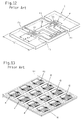
- the strain sensor E of the above described structure is prepared, as shown in Fig. 13, from a relatively large plate material H having one surface formed with a plurality of strain detecting elements G each having a pair of the strain sensing areas G1 and arranged in a matrix pattern, which strain detecting elements G are subsequently separated from each other by means of a laser beam cutting technique to provide the individual strain sensors E each being shown in Fig. 13.
- a cutting line along which the plate material H has to be cut by means of the laser beam cutting technique to provide the individual strain sensors E is so complicated as shown by the phantom line in Fig. 13 and, therefore, the cutting involves a complicated and time-consuming procedures to such an extent as to result in a reduction in productivity of the strain sensors E.
- a YAG laser is generally used during the cutting of the plate material H to provide the individual strain sensors E since the YAG laser is superior in that it brings about little thermal influence on the surroundings.
- the laser beam is traversed in close proximity to the individual strain sensing areas G1 which are most sensible and important areas and, therefore, there is no way to avoid a thermal influence on the strain sensing areas G1. Therefore, it often occurs that some of the resultant strain sensors E are found defective and/or are liable of a reduction in detecting accuracy.
- the present invention is intended to provide an improved strain sensor of either a three-beam type or a two-beam type which can be advantageously used in a load cell or an accelerometer and which can be manufactured in high productivity, capable of exhibiting a high detecting accuracy stably at all times.
- the present invention provides a method of manufacturing individual strain sensors each comprised of a generally rectangular substrate having first and second major surfaces opposite to each other, a strain detecting element formed on the first major surface of the substrate and having at least one pair of strain sensing areas, and a pair of grooves defining respective areas of low rigidity and formed in the second major surface of the substrate at respective locations adjacent the opposite ends of the substrate while extending across the width of the substrate with the strain sensing areas of the strain detecting element positioned in register with the respective grooves.
- these strain sensors are prepared from a single plate material of any suitable size having first and second surfaces opposite to each other and eventually forming respective substrates of the individual strain sensors.
- a plurality of groove segments spaced a predetermined distance from each other are then formed on the second surface of the plate material so as to extend parallel to each other, and a plurality of strain detecting elements are subsequently on the first surface of the plate material in a substantially matrix pattern so as to assume a predetermined positional relationship with respective positions of the groove segments.
- the plate material is cut along cutting lines extending in two different directions to separate the individual strain sensors.
- the strain detecting elements are formed on the first surface of the plate material in any known manner so as to assume the predetermined positional relationship with the respective positions of the groove segments, the subsequent cutting of the plate material along the cutting lines extending in the two different directions, i.e., widthwise and lengthwise of the plate material, results in separation of the individual strain sensors. Therefore, as compared with the prior art method of cutting to provide strain sensors each having notches, the cutting job is extremely easy to perform and the productivity of the strain sensors is increased accordingly.
- the pair of the regions of low rigidity in the rectangular substrate positioned adjacent the respective opposite ends of the rectangular substrate are defined by the grooves formed on the second major surface of the substrate opposite to the first major surface where the strain detecting element is formed. Accordingly, the sensitivity of the strain sensor to the strain is determined by the wall thickness of that portion of the substrate where each area of low rigidity is defined, and therefore, by properly choosing the wall thickness of that portion of the substrate, a required sensitivity to the strain can be obtained. This means that a compact strain sensor capable of exhibiting an accurate sensing performance can be manufactured with no need to employ the substrate of an increased width such as required in the prior art strain sensor.
- the use of the compact strain sensor provided for by the method of the present invention contributes to a reduction in size of the load cell or accelerometer utilizing the strain sensor. Also, where the strain sensors are prepared from a single plate material, the number of the strain sensors which can be prepared from the single plate material can be increased, accompanied by an increase of the productivity and a reduction in cost.
- the distance defined between each cutting line extending in one of the two directions and each of the strain sensing areas of each of the strain detecting elements and the distance defined between each cutting line extending in the other of the two directions and each of the strain sensing areas of such strain detecting element are so chosen as to provide a respective marginal area sufficient to prevent the strain detecting element from being adversely affected during an execution of the cutting step along the cutting lines.
- This is particularly advantageous in that the strain sensing areas can be isolated from any possible adverse effect which would otherwise be brought about when the laser beam traverses in close proximity of the strain sensing areas during an execution of the cutting process. The result is that the highly accurate strain sensor can be obtained.
- terminal elements for electrically connecting the strain detecting element with an external signal processing device are formed on the first surface of the plate material at a location between the strain sensing areas of each of the strain detecting elements and adjacent the cutting line corresponding to one side edge of the substrate of each eventually formed strain sensor.
- the plate elements having the plural strain detecting elements may be cut by machining to provide the individual strain sensors, the use of a laser beam is particularly preferred since the plate material can be cut to a high precision while providing a smooth cut face.
- the grooves can be formed easily by means of an etching process.
- an electrically insulating layer is to be formed on the first surface of the plate material prior to the formation of the strain detecting elements so that no electric contact occurs between the strain detecting elements and the plate material.
- the illustrated load cell comprises a elastic element 10 of a hollow box-like configuration.
- This elastic element 10 is of a substantially three-layered structure which includes upper and lower plate members 11 and 12 of a generally U-shaped cross-section, each prepared from a metallic plate and having a pair of side flanges 11a or 12a integrally formed therewith, and a generally rectangular intermediate plate member 13 having its opposite side portions fixedly sandwiched between the side flanges 11a of the upper plate member 11 and the side flanges 12a of the lower plate member 12.
- respective portions of the upper plate member 11 and the lower plate member 12 intermediate between the opposite ends, that is, the stationary and movable rigid bodies 14 and 15 of the elastic element 1 form respective beams 16 and 17.
- Each of the beams 16 and 17 has a pair of notches 16a or 17a positioned adjacent the stationary and movable rigid bodies 14 and 15, said notches 16a or 17a of each pair extending in alignment with each other in a direction widthwise of the associated plate member 11 or 12 so as to leave a respective neck region 16b or 17b of low rigidity.
- the intermediate plate member 13 has an opening 13a defined therein at a location intermediate of the length thereof, and a generally rectangular strain sensor 20 is mounted in said opening 13a with its opposite ends fixedly secured to opposite portions of the intermediate plate member 13 around the opening 13a and with its longitudinal axis aligned with the longitudinal axis of the intermediate plate member 13.
- the stationary rigid body 14 when in use, the stationary rigid body 14 is fixedly secured to a bench A, for example, a housing framework of a weighing apparatus, while the movable rigid body 15 is coupled with a weighing table B. Placement of a load W of an object C to be weighed on the weighing table B results in a flexure of the upper and lower beams 16 and 17 about the respective neck regions 16b and 17b of low rigidity in a direction generally perpendicular to the lengthwise direction of each beam 16 and 17 as shown by the phantom line in Fig. 1b with the movable rigid body 15 displaced downwardly, as viewed in Fig.
- the strain sensor 20 comprises a generally rectangular substrate 21 made of metal such as, for example, stainless steel, and a strain detecting element 23 formed on one of first and second opposite major surfaces, for example, the first major surface, of the substrate 21 through an insulating layer 22 made of electrically insulating material such as, for example, polyester or polyimide.
- the second major surface of the substrate 21 is formed with grooves 14 positioned adjacent the opposite ends of the substrate 21 and extending across the width thereof so as to leave respective reduced thickness areas which define associated areas 21a of low rigidity of the substrate 21.
- the strain detecting element 23 referred to above includes a pair of strain sensing areas 23a each in the form of a resistance wiring and positioned substantially in register with the associated groove 24 in the substrate 21, a generally L-shaped first conductor 23b electrically connecting one end of one of the strain sensing areas 23a with a first terminal element 23c, a generally L-shaped second conductor 23b electrically connecting one end of the other of the strain sensing areas 23a with a second terminal element 23c, and a generally T-shaped third conductor 23b electrically connecting the other ends of the respective strain sensing areas 23a with a third terminal element 23c.
- This strain detecting element 23 is so designed and so configured as to provide a so-called half-bridge circuit, said terminal elements 23c being positioned adjacent one side portion of the substrate 21. It is to be noted that the distance L3 between each end 21b of the substrate 21 and the adjacent strain sensing area 23a of the strain detecting element 23 and the distance L4 between each side edge 21c of the substrate 21 and the adjacent strain sensing area 23a of the strain detecting element 23 are so sized as to provide a marginal area sufficient to prevent each strain sensing areas 23a from being adversely affected by heat evolved during the cutting process as will be described later.
- the resistance values of the respective strain sensing areas 23a correspondingly vary, i.e., increases or decreases.
- a change in resistance value of each strain sensing area 23a is outputted to an external signal processing device (not shown) through a cable 25 shown in Fig. 1a having respective lines electrically connected with the first to third terminal elements 23c as shown in Fig. 2, which signal processing device performs a calculation to determine the magnitude of the load which has resulted in the deformation of the elastic element 10 and, hence, that of the substrate 21 of the strain sensor 20.
- disposition of the first to third terminal elements 23c adjacent the side edge 21c of the substrate 21 makes it possible to connect the first to third terminal elements 23c with the external signal processing device through the cable 25 without permitting the cable 25 to interfere any one of the strain sensing areas 23a while providing a sufficient space for the electric connection.
- the sensitivity of the strain sensor 20 to the induced strain depends on the depth of each of the grooves 24 which define the areas 21a of low rigidity in the substrate 21, that is, the wall thickness of that portion of the substrate 21 where each area 21a of low rigidity is defined, and therefore, by properly choosing the wall thickness of that portion of the substrate 21, a required sensitivity to the strain can be obtained. Accordingly, it is possible to reduce the width L1 of the substrate 21 to such a value as required in forming the strain detecting element 23 and, therefore, the strain sensor 20 and, hence, the load cell as a whole can be manufactured compact in size.
- a plurality of parallel grooves 31 are formed on one surface (a second surface) of the plate material 30 with a predetermined space between the neighboring grooves as shown in Fig. 3.
- any known machining process may be employed.
- a half-etching technique which is one of the know etching methods is employed and practiced in the following manner.
- a resist film 32 is formed on the surface of the plate material 30, followed by a placement of a patterned masking film 33 over the resist film 32.
- the patterned masking film 33 has a pattern of light shielding areas 33a and light transmissive areas 33b alternating with the light shielding areas 33a, said light shielding areas 33a corresponding in position to the grooves 31 which are eventually formed in the plate material 30.
- the plate material 30 having the resist film 32 covered by the patterned masking film 33 is subsequently exposed to light from above so that respective portions of the resist film 32 in register with the light transmissive areas 33b of the patterned masking film 33 can be cured.
- the patterned masking film 33 is then removed off, or otherwise removed in any suitable manner, from the plate material 30 and the non-cured areas of the resist film 32 which have been registered with the light shielding areas 33a of the patterned masking film 33 are removed in contact with a developing solution of a predetermined composition, thereby leaving only the cured portions 32a of the resist film 32 on the surface of the plate material 30.
- portions of the plate material 30 where the resist layer 32 no longer exist are etched off to a desired depth to thereby form the grooves 31 in that surface of the plate material 30, followed by removal of the cured portions 32a of the resist layer 32 to complete the grooved plate material 30 such as shown in Fig. 3.
- a plurality of strain detecting elements 23 are, as shown in Fig. 7, formed on the surface of the grooved plate material 30 opposite to that surface where the grooves 31 have been formed, in a substantially matrix pattern through electrically insulating layers 22 intervening between each strain detecting element 23 and the opposite surface of the grooved plate material 30.
- the formation of the strain detecting elements 23 is carried out by repeating, for example, a sputtering process to form a metallic thin film and an etching process to configure the metallic thin film into a predetermined pattern so that, as schematically shown in Fig. 8, a multi-layered structure including at least the strain sensing areas 23a and the conductors 23b are formed.
- the plate material 30 having the strain detecting elements 23 so formed on that surface thereof are covered by a protective film 23d which may be formed by the use of any known screen printing technique, except for the terminal elements 23c.
- each of the strain detecting elements 23 is so positioned that the pair of the strain sensing areas 23a can occupy respective positions in register with the grooves 31 formed on the surface of the plate material 30 opposite to the surface where the strain detecting elements 23 have been formed.
- the plate material 30 having the grooves 31 formed on one surface thereof and the plural strain sensing elements 23 formed on the opposite surface (a first surface) thereof is cut along a grid pattern of cutting lines b shown by the phantom line in Fig. 7 to thereby separate the individual strain sensing elements 23 each being of the construction shown in Fig. 2.
- the cutting lines b define opposite ends and opposite side edges of each of the strain detecting elements 23 when the latter are separated from each other. Since the cutting lines b merely consist of lines extending widthwise of the plate material 30 and transverse lines extending lengthwise of the plate material 30, the cutting process can extremely easily be performed enough to increase the productivity.
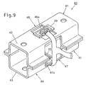
- strain sensor according to the present invention is utilizable not only in the load cell of the three-beam type as shown in Fig. 1, but also in the load cell of the two-beam type as shown in any one of Fig. 9.
- the load cell shown in Fig. 9 and now identified by 40 comprises a elastic element 41 of a hollow box-like configuration.
- This elastic element 41 is of a substantially two-layered structure which includes upper and lower plate members 42 and 43 of a generally U-shaped cross-section, each prepared from a metallic plate and having a pair of side flanges 42a or 43a, said upper and lower plate members 42 and 42 being connected together with the respective pairs of the side flanges 42a and 43a welded together.
- One end of the elastic element 41 that is, a portion of the elastic element 41 defined by respective one ends of the upper plate member 42 and the lower plate member 43 forms a stationary rigid body 44 while the opposite end of the elastic element 41, that is, an opposite portion of the elastic element 41 defined by respective other ends of the upper plate member 42 and the lower plate member 43 forms a movable rigid body 45, while respective portions of the upper plate member 42 and the lower plate member 43 intermediate between the opposite ends, that is, the stationary and movable rigid bodies 44 and 45 of the elastic element 41 form respective beams 46 and 47.
- Each of the upper and lower beams 46 and 47 has a generally rectangular opening 46a or 47a defined therein at a location intermediate of the length thereof, and carries a generally rectangular strain sensor 20 mounted in said opening 46a or 47a with its opposite ends fixedly secured to opposite portions of the associated plate member 42 or 43 around the opening 46a or 47a and with its longitudinal axis aligned with the longitudinal axis of the associated plate member 42 or 43.
- each strain sensor 20 or 20A has been shown as a half bridge circuit design in which the two strain sensing areas are employed. However, as shown in Fig. 11, four strain sensing areas for each strain sensor may be formed on a single substrate to provide the strain sensor, now identified by 60, of the full bridge circuit design.
- the strain sensor 60 of the full bridge circuit design shown in Fig. 10 is comprised of, as is the case with the strain sensor 20 shown and described in connection with the foregoing embodiment of the present invention, a generally rectangular substrate 61 having one surface formed with a pair of transverse grooves 64 extending widthwise of the substrate 61 adjacent the opposite ends thereof to define respective areas 61a of low rigidity and also having the opposite surface deposited with a strain detecting element 63 through an electrically insulating layer 62.
- the strain detecting element 63 so formed on the opposite surface of the substrate 61 has a pair of strain sensing areas 63a defined in register with each transverse groove 64 and, hence, has four strain sensing areas 63a in total number.
- the two strain sensing areas 63a are arranged in a direction widthwise of the substrate 61 in register with each area 61a of low rigidity. If notches are to be formed in the direction widthwise of the substrate to form an area of low rigidity in the substrate as is the case with the prior art, the substrate must have an increased width. However, according to the present invention, the necessity of use of the substrate having an increased width can be avoided, making it possible to provide a highly precise strain sensor of the full bridge circuit design that is compact in size.
- a method of manufacturing individual strain sensors (20) each comprised of a generally rectangular substrate (21) having first and second major surfaces opposite to each other, a strain detecting element (23) formed on the first major surface of the substrate and having at least one pair of strain sensing areas (23a), and a pair of grooves (24) defining respective areas (21a) of low rigidity and formed in the second major surface of the substrate (21) at respective locations adjacent the opposite ends of the substrate (21) while extending across the width of the substrate with the strain sensing areas (23a) of the strain detecting element (23) positioned in register with the respective grooves (24).
- the strain sensors (20) are prepared from a single plate material (30) of any suitable size having first and second surfaces opposite to each other and eventually forming respective substrates (21) of the individual strain sensors (20).
- a plurality of spaced groove segments (31) are formed on the second surface of the plate material (30) so as to extend parallel to each other, and a plurality of strain detecting elements (23) are subsequently formed on the first surface of the plate material (30) in a substantially matrix pattern so as to assume a predetermined positional relationship with respective positions of the groove segments (31). Thereafter, the plate material (30) is cut along cutting lines (b) extending in two different directions to separate the individual strain sensors (20).
Abstract
Description
- The present invention relates to a strain sensor of a type generally useable in various load cells for detecting the weight of an object to be weighed or an accelerometer and, more specifically, to a method of manufacturing such strain sensor.
- A load cell generally used in a weight detecting apparatus such as, for example, an electronic scale makes use of a elastic element of a generally hollow rectangular configuration comprising stationary and movable rigid bodies defined at opposite ends thereof and upper and lower beams extending between the rigid bodies while spaced a distance from each other, each of said upper and lower beams having a region of low rigidity. The stationary rigid body is fixedly secured to a support such as, for example, a housing framework of the apparatus and the movable rigid body is adapted to receive a load of which weight is desired to be measured. When in use the load is applied to the movable rigid body of the elastic element through, for example, a weighing table, the movable rigid body displaces relative to the stationary rigid body in a quantity proportional to the weight of the load, accompanied by the upper and lower beams yielding at the respective regions of low rigidity. By detecting a tensile strain or a compressive strain developed at the regions of low rigidity of the beams as a result of the relative displacement between the stationary and movable rigid bodies, an indication of the weight of the load applied can be obtained.
- A sophisticated version of the load cell of a three-beam design is now conceived by the applicant. This prior art three-beam type load cell is shown in Fig. 11 of the accompanying drawings. Referring to Fig. 11 for the discussion of the prior art, the three-beam type load cell shown therein comprises a elastic element D of a generally parallelopiped configuration including rigid bodies A defined at opposite ends thereof, upper and lower beams B extending between the rigid bodies A in parallel relation to each other, each of said beams B having a pair of regions of low rigidity B1, and arms C extending from the respective rigid bodies A into a space, delimited by the rigid bodies A and the beams B, in alignment with each other in a direction close towards each other. A strain sensor E is fitted at its opposite ends to the respective arms C so that the elastic element D as a whole represents a three-layered structure. When in use a displacement of one of the rigid bodies A relative to the other of the rigid bodies A in a direction generally perpendicular to any one of the beams B results in a tensile strain or a compressive strain developed on the surface of a substrate of the strain sensor E, and a subsequent detection of the strain so developed on the strain sensor can provide an indication of the magnitude of the load applied, that is, the weight of an object having been weighed.
- The strain sensor E employed is well known is manufactured by the following manner which will now be described with reference to Fig. 12. Namely, a generally rectangular substrate F has its opposite ends adapted to be fixedly secured to the respective arms C of the elastic element D as shown in Fig. 11. This substrate F has two pairs of generally U-shaped notches F1 formed therein with each pair adjacent the corresponding end of the substrate E while the notches F1 of each pair extend inwardly of the substrate E from opposite side edges of the substrate E in alignment with each other so as to leave an associated neck region F2 having a low rigidity. A detecting element G having a pair of strain sensing areas C1 each comprised of a fine resistance wiring is deposited on an upper surface of the substrate E with the strain sensing areas C1 positioned respective surface portions of the substrate E where the associated neck regions F2 are defined.
- It has however been found that, in the case of the strain sensor E of the structure described above, the amount of strains induced in each of the neck regions F2 of low rigidity as a result of application of a load, that is, the magnitude of an output from the detecting element G or the sensitivity to the strain depends on the ratio (L1/L2) of the width L1 of the substrate F relative to the width L2 of each of the neck regions F2 of low rigidity left by the respective pairs of the U-shaped notches F1. Accordingly, in order to increase the sensitivity to the strain, either must the width L1 of the substrate F be increased, or the width L2 of each of the neck regions F2 of low rigidity must be reduced. However, in view of the fact that the strain sensing areas G1 of the strain detecting element G are formed on the substrate F between the respective pairs of the U-shaped notches F1, that is, on the respective neck regions F2 of low rigidity, reduction in width L2 of each of the neck regions F2 of low rigidity is limited practically. Hence, a practical compromise to increase the sensitivity to the strain is to employ the substrate F having an increased width L1, and this in turn results in an increase in size of the strain sensor.
- Also, the strain sensor E of the above described structure is prepared, as shown in Fig. 13, from a relatively large plate material H having one surface formed with a plurality of strain detecting elements G each having a pair of the strain sensing areas G1 and arranged in a matrix pattern, which strain detecting elements G are subsequently separated from each other by means of a laser beam cutting technique to provide the individual strain sensors E each being shown in Fig. 13. In such case, since two pairs of notches F1 must be formed for each resultant strain sensor E, a cutting line along which the plate material H has to be cut by means of the laser beam cutting technique to provide the individual strain sensors E is so complicated as shown by the phantom line in Fig. 13 and, therefore, the cutting involves a complicated and time-consuming procedures to such an extent as to result in a reduction in productivity of the strain sensors E.
- There is an additional problem. A YAG laser is generally used during the cutting of the plate material H to provide the individual strain sensors E since the YAG laser is superior in that it brings about little thermal influence on the surroundings. However, during the formation of the notches F1, the laser beam is traversed in close proximity to the individual strain sensing areas G1 which are most sensible and important areas and, therefore, there is no way to avoid a thermal influence on the strain sensing areas G1. Therefore, it often occurs that some of the resultant strain sensors E are found defective and/or are liable of a reduction in detecting accuracy.
- In view of the foregoing, the present invention is intended to provide an improved strain sensor of either a three-beam type or a two-beam type which can be advantageously used in a load cell or an accelerometer and which can be manufactured in high productivity, capable of exhibiting a high detecting accuracy stably at all times.
- To this end, the present invention provides a method of manufacturing individual strain sensors each comprised of a generally rectangular substrate having first and second major surfaces opposite to each other, a strain detecting element formed on the first major surface of the substrate and having at least one pair of strain sensing areas, and a pair of grooves defining respective areas of low rigidity and formed in the second major surface of the substrate at respective locations adjacent the opposite ends of the substrate while extending across the width of the substrate with the strain sensing areas of the strain detecting element positioned in register with the respective grooves.
- According to the present invention, these strain sensors are prepared from a single plate material of any suitable size having first and second surfaces opposite to each other and eventually forming respective substrates of the individual strain sensors. A plurality of groove segments spaced a predetermined distance from each other are then formed on the second surface of the plate material so as to extend parallel to each other, and a plurality of strain detecting elements are subsequently on the first surface of the plate material in a substantially matrix pattern so as to assume a predetermined positional relationship with respective positions of the groove segments. Thereafter, the plate material is cut along cutting lines extending in two different directions to separate the individual strain sensors.
- In the practice of the method of the present invention, if after the formation of the parallel groove segments on the second surface of the plate material, which groove segments eventually form the areas of low rigidity in the substrate of each strain sensor, the strain detecting elements are formed on the first surface of the plate material in any known manner so as to assume the predetermined positional relationship with the respective positions of the groove segments, the subsequent cutting of the plate material along the cutting lines extending in the two different directions, i.e., widthwise and lengthwise of the plate material, results in separation of the individual strain sensors. Therefore, as compared with the prior art method of cutting to provide strain sensors each having notches, the cutting job is extremely easy to perform and the productivity of the strain sensors is increased accordingly.
- In each strain sensor manufactured according to the method of the present invention, the pair of the regions of low rigidity in the rectangular substrate positioned adjacent the respective opposite ends of the rectangular substrate are defined by the grooves formed on the second major surface of the substrate opposite to the first major surface where the strain detecting element is formed. Accordingly, the sensitivity of the strain sensor to the strain is determined by the wall thickness of that portion of the substrate where each area of low rigidity is defined, and therefore, by properly choosing the wall thickness of that portion of the substrate, a required sensitivity to the strain can be obtained. This means that a compact strain sensor capable of exhibiting an accurate sensing performance can be manufactured with no need to employ the substrate of an increased width such as required in the prior art strain sensor. The use of the compact strain sensor provided for by the method of the present invention contributes to a reduction in size of the load cell or accelerometer utilizing the strain sensor. Also, where the strain sensors are prepared from a single plate material, the number of the strain sensors which can be prepared from the single plate material can be increased, accompanied by an increase of the productivity and a reduction in cost.
- Where the cutting lines along which the plate material is to be cut to provide the individual strain sensors extend perpendicular to each other and in the respective direction widthwise and lengthwise of the plate material, the cutting process can easily be performed.
- Preferably, the distance defined between each cutting line extending in one of the two directions and each of the strain sensing areas of each of the strain detecting elements and the distance defined between each cutting line extending in the other of the two directions and each of the strain sensing areas of such strain detecting element are so chosen as to provide a respective marginal area sufficient to prevent the strain detecting element from being adversely affected during an execution of the cutting step along the cutting lines. This is particularly advantageous in that the strain sensing areas can be isolated from any possible adverse effect which would otherwise be brought about when the laser beam traverses in close proximity of the strain sensing areas during an execution of the cutting process. The result is that the highly accurate strain sensor can be obtained.
- Also preferably, terminal elements for electrically connecting the strain detecting element with an external signal processing device are formed on the first surface of the plate material at a location between the strain sensing areas of each of the strain detecting elements and adjacent the cutting line corresponding to one side edge of the substrate of each eventually formed strain sensor. By so doing, a maximized utilization of a space is possible for connecting lines leading from the external signal processing device with the strain detecting element.
- Although the plate elements having the plural strain detecting elements may be cut by machining to provide the individual strain sensors, the use of a laser beam is particularly preferred since the plate material can be cut to a high precision while providing a smooth cut face.
- The grooves can be formed easily by means of an etching process.
- Where the plate material is made of metal such as, for example, stainless steel or aluminum, an electrically insulating layer is to be formed on the first surface of the plate material prior to the formation of the strain detecting elements so that no electric contact occurs between the strain detecting elements and the plate material.
- In any event, the present invention will become more clearly understood from the following description of preferred embodiments thereof, when taken in conjunction with the accompanying drawings. However, the embodiments and the drawings are given only for the purpose of illustration and explanation, and are not to be taken as limiting the scope of the present invention in any way whatsoever, which scope is to be determined by the appended claims. In the accompanying drawings, like reference numerals are used to denote like parts throughout the several views, and:
- Fig. 1a is a perspective view, with a portion cut away, showing an example of a load cell in which a strain sensor manufactured according to a method of the present invention can be employed;
- Fig. 1b is schematic side view showing the manner in which the load cell operates;
- Fig. 2 is a perspective view of the strain sensor;
- Fig. 3 is a perspective view showing a plate material which eventually forms substrates for the strain sensors and in which grooves are formed during the practice of the method according to one preferred embodiment of the present invention;
- Fig. 4 is a side sectional view, on an enlarged scale, showing a first step of an etching method for forming the grooves in the plate material;
- Fig. 5 is a side sectional view, on an enlarged scale, showing a second step of the etching method for forming the grooves;
- Fig. 6 is a side sectional view, on an enlarged scale, showing a third step of the etching method for forming the grooves;
- Fig. 7 is a schematic perspective view of the plate material in which a plurality of strain detecting elements are formed;
- Fig. 8 is a side sectional view, on an enlarged scale, showing the structure of one of the strain detecting elements formed on the plate material;
- Fig. 9 is a perspective view showing another example of the load cell in which the strain sensor shown in Fig. 1a is employed;
- Fig. 10 is a top plan view showing another example of the strain sensor manufactured according to the method of the present invention;
- Fig. 11 is a perspective view showing a three-beam type load cell;
- Fig. 12 is a perspective view showing the prior art strain sensor; and
- Fig. 13 is a perspective view showing one step of the method of manufacturing the prior art strain sensor.
- With reference to Fig. 1a, the load cell in which a strain sensor according to the present invention may be employed will first be described in detail. The illustrated load cell, generally identified by 1, comprises a
elastic element 10 of a hollow box-like configuration. Thiselastic element 10 is of a substantially three-layered structure which includes upper andlower plate members side flanges intermediate plate member 13 having its opposite side portions fixedly sandwiched between theside flanges 11a of theupper plate member 11 and theside flanges 12a of thelower plate member 12. - One end of the
elastic element 1, that is, a portion of theelastic element 1 defined by respective one ends of theupper plate member 11, thelower plate member 12 and theintermediate plate member 13, forms a stationaryrigid body 14 while the opposite end of theelastic element 1, that is, an opposite portion of theelastic element 1 defined by respective other ends of theupper plate member 11, thelower plate member 12 and theintermediate plate member 13, forms a movablerigid body 15. - In this construction, respective portions of the
upper plate member 11 and thelower plate member 12 intermediate between the opposite ends, that is, the stationary and movablerigid bodies elastic element 1 formrespective beams beams notches rigid bodies notches plate member respective neck region intermediate plate member 13 has anopening 13a defined therein at a location intermediate of the length thereof, and a generallyrectangular strain sensor 20 is mounted in saidopening 13a with its opposite ends fixedly secured to opposite portions of theintermediate plate member 13 around theopening 13a and with its longitudinal axis aligned with the longitudinal axis of theintermediate plate member 13. - As shown in Fig. 1b, when in use, the stationary
rigid body 14 is fixedly secured to a bench A, for example, a housing framework of a weighing apparatus, while the movablerigid body 15 is coupled with a weighing table B. Placement of a load W of an object C to be weighed on the weighing table B results in a flexure of the upper andlower beams respective neck regions beam rigid body 15 displaced downwardly, as viewed in Fig. 1b, relative to the stationaryrigid body 14, accompanied by a corresponding flexure of thestrain sensor 20 carried by theintermediate plate member 13. As thestrain sensor 20 is so deformed, one end of thestrain sensor 20 adjacent the movablerigid body 15 is correspondingly displaced downwardly relative to the opposite end of thestrain sensor 20 adjacent the stationaryrigid body 14 with tensile and compressive strains consequently induced on a surface of a substrate forming a part of thestrain sensor 20. By detecting the tensile and compressive strains induced in thestrain sensor 20, the load applied to the movablerigid body 15 can be measured. - The structure of the
strain sensor 20 will now be described in detail with particular reference to Fig. 2. As shown therein, thestrain sensor 20 comprises a generallyrectangular substrate 21 made of metal such as, for example, stainless steel, and astrain detecting element 23 formed on one of first and second opposite major surfaces, for example, the first major surface, of thesubstrate 21 through an insulatinglayer 22 made of electrically insulating material such as, for example, polyester or polyimide. The second major surface of thesubstrate 21 is formed withgrooves 14 positioned adjacent the opposite ends of thesubstrate 21 and extending across the width thereof so as to leave respective reduced thickness areas which define associatedareas 21a of low rigidity of thesubstrate 21. - The
strain detecting element 23 referred to above includes a pair ofstrain sensing areas 23a each in the form of a resistance wiring and positioned substantially in register with the associatedgroove 24 in thesubstrate 21, a generally L-shapedfirst conductor 23b electrically connecting one end of one of thestrain sensing areas 23a with a firstterminal element 23c, a generally L-shapedsecond conductor 23b electrically connecting one end of the other of thestrain sensing areas 23a with a secondterminal element 23c, and a generally T-shapedthird conductor 23b electrically connecting the other ends of the respectivestrain sensing areas 23a with a thirdterminal element 23c. Thisstrain detecting element 23 is so designed and so configured as to provide a so-called half-bridge circuit, saidterminal elements 23c being positioned adjacent one side portion of thesubstrate 21. It is to be noted that the distance L3 between eachend 21b of thesubstrate 21 and the adjacentstrain sensing area 23a of thestrain detecting element 23 and the distance L4 between eachside edge 21c of thesubstrate 21 and the adjacentstrain sensing area 23a of thestrain detecting element 23 are so sized as to provide a marginal area sufficient to prevent eachstrain sensing areas 23a from being adversely affected by heat evolved during the cutting process as will be described later. - When as a result of deformation of the
elastic element 10 shown in Fig. 1a the tensile strain and the compressive strain are induced in a surface region of one of theareas 21a of low rigidity of thesubstrate 21 shown in Fig. 2 and a surface region of the other of theareas 21a of low rigidity of thesubstrate 21, respectively, the resistance values of the respectivestrain sensing areas 23a correspondingly vary, i.e., increases or decreases. A change in resistance value of eachstrain sensing area 23a is outputted to an external signal processing device (not shown) through acable 25 shown in Fig. 1a having respective lines electrically connected with the first to thirdterminal elements 23c as shown in Fig. 2, which signal processing device performs a calculation to determine the magnitude of the load which has resulted in the deformation of theelastic element 10 and, hence, that of thesubstrate 21 of thestrain sensor 20. - As hereinabove described, disposition of the first to third
terminal elements 23c adjacent theside edge 21c of thesubstrate 21 makes it possible to connect the first to thirdterminal elements 23c with the external signal processing device through thecable 25 without permitting thecable 25 to interfere any one of thestrain sensing areas 23a while providing a sufficient space for the electric connection. - In the
strain sensor 20 of the above described construction, the sensitivity of thestrain sensor 20 to the induced strain depends on the depth of each of thegrooves 24 which define theareas 21a of low rigidity in thesubstrate 21, that is, the wall thickness of that portion of thesubstrate 21 where eacharea 21a of low rigidity is defined, and therefore, by properly choosing the wall thickness of that portion of thesubstrate 21, a required sensitivity to the strain can be obtained. Accordingly, it is possible to reduce the width L1 of thesubstrate 21 to such a value as required in forming thestrain detecting element 23 and, therefore, thestrain sensor 20 and, hence, the load cell as a whole can be manufactured compact in size. - Hereinafter, a method of making the
strain sensor 20 of the above described construction will be described. - Given a
rectangular plate material 30 of a suitable size made of metal such as, for example, stainless steel, a plurality ofparallel grooves 31 are formed on one surface (a second surface) of theplate material 30 with a predetermined space between the neighboring grooves as shown in Fig. 3. To form theseparallel grooves 31 in theplate material 30, any known machining process may be employed. However, in the illustrated embodiment of the present invention, a half-etching technique which is one of the know etching methods is employed and practiced in the following manner. - At the outset, as shown in Fig. 4, a resist
film 32 is formed on the surface of theplate material 30, followed by a placement of apatterned masking film 33 over the resistfilm 32. The patternedmasking film 33 has a pattern oflight shielding areas 33a and lighttransmissive areas 33b alternating with thelight shielding areas 33a, saidlight shielding areas 33a corresponding in position to thegrooves 31 which are eventually formed in theplate material 30. Theplate material 30 having the resistfilm 32 covered by the patternedmasking film 33 is subsequently exposed to light from above so that respective portions of the resistfilm 32 in register with thelight transmissive areas 33b of the patternedmasking film 33 can be cured. - The patterned
masking film 33 is then removed off, or otherwise removed in any suitable manner, from theplate material 30 and the non-cured areas of the resistfilm 32 which have been registered with thelight shielding areas 33a of the patternedmasking film 33 are removed in contact with a developing solution of a predetermined composition, thereby leaving only the curedportions 32a of the resistfilm 32 on the surface of theplate material 30. - Thereafter, as shown in Fig. 6, using any known etching process, portions of the
plate material 30 where the resistlayer 32 no longer exist are etched off to a desired depth to thereby form thegrooves 31 in that surface of theplate material 30, followed by removal of the curedportions 32a of the resistlayer 32 to complete thegrooved plate material 30 such as shown in Fig. 3. - Subsequent to the formation of the
grooves 31 in that surface of theplate material 30, a plurality ofstrain detecting elements 23 are, as shown in Fig. 7, formed on the surface of thegrooved plate material 30 opposite to that surface where thegrooves 31 have been formed, in a substantially matrix pattern through electrically insulatinglayers 22 intervening between eachstrain detecting element 23 and the opposite surface of thegrooved plate material 30. - The formation of the
strain detecting elements 23 is carried out by repeating, for example, a sputtering process to form a metallic thin film and an etching process to configure the metallic thin film into a predetermined pattern so that, as schematically shown in Fig. 8, a multi-layered structure including at least thestrain sensing areas 23a and theconductors 23b are formed. Theplate material 30 having thestrain detecting elements 23 so formed on that surface thereof are covered by aprotective film 23d which may be formed by the use of any known screen printing technique, except for theterminal elements 23c. At this time, each of thestrain detecting elements 23 is so positioned that the pair of thestrain sensing areas 23a can occupy respective positions in register with thegrooves 31 formed on the surface of theplate material 30 opposite to the surface where thestrain detecting elements 23 have been formed. - Thereafter, the
plate material 30 having thegrooves 31 formed on one surface thereof and the pluralstrain sensing elements 23 formed on the opposite surface (a first surface) thereof is cut along a grid pattern of cutting lines b shown by the phantom line in Fig. 7 to thereby separate the individualstrain sensing elements 23 each being of the construction shown in Fig. 2. As a matter of course, the cutting lines b define opposite ends and opposite side edges of each of thestrain detecting elements 23 when the latter are separated from each other. Since the cutting lines b merely consist of lines extending widthwise of theplate material 30 and transverse lines extending lengthwise of theplate material 30, the cutting process can extremely easily be performed enough to increase the productivity. - Even where a laser beam is employed in the practice of the cutting process, and since the distances L3 and L4 between the cutting lines b and each
strain sensing area 23a are so chosen as to have respective values sufficient to prevent eachstrain sensing area 23a from being adversely affected by heat brought about the laser beam, the laser beam will not traverse in close proximity to eachstrain sensing area 23a and, therefore, the highlyaccurate strain sensors 20 can be obtained at all times. - It is to be noted that the strain sensor according to the present invention is utilizable not only in the load cell of the three-beam type as shown in Fig. 1, but also in the load cell of the two-beam type as shown in any one of Fig. 9.
- More specifically, the load cell shown in Fig. 9 and now identified by 40 comprises a
elastic element 41 of a hollow box-like configuration. Thiselastic element 41 is of a substantially two-layered structure which includes upper andlower plate members lower plate members elastic element 41, that is, a portion of theelastic element 41 defined by respective one ends of theupper plate member 42 and thelower plate member 43 forms a stationaryrigid body 44 while the opposite end of theelastic element 41, that is, an opposite portion of theelastic element 41 defined by respective other ends of theupper plate member 42 and thelower plate member 43 forms a movablerigid body 45, while respective portions of theupper plate member 42 and thelower plate member 43 intermediate between the opposite ends, that is, the stationary and movablerigid bodies elastic element 41 formrespective beams lower beams rectangular opening rectangular strain sensor 20 mounted in saidopening plate member opening plate member - Thus, it will readily be seen that in the
load cell 40 shown in Fig. 9, the twostrain sensors 20 each having the two strain sensing areas are employed completing the strain detecting element of a so-called full bridge circuit design. - It is to be noted that, in any one of the foregoing examples of the load cells, each
strain sensor 20 or 20A has been shown as a half bridge circuit design in which the two strain sensing areas are employed. However, as shown in Fig. 11, four strain sensing areas for each strain sensor may be formed on a single substrate to provide the strain sensor, now identified by 60, of the full bridge circuit design. - The
strain sensor 60 of the full bridge circuit design shown in Fig. 10 is comprised of, as is the case with thestrain sensor 20 shown and described in connection with the foregoing embodiment of the present invention, a generallyrectangular substrate 61 having one surface formed with a pair oftransverse grooves 64 extending widthwise of thesubstrate 61 adjacent the opposite ends thereof to definerespective areas 61a of low rigidity and also having the opposite surface deposited with astrain detecting element 63 through an electrically insulatinglayer 62. Thestrain detecting element 63 so formed on the opposite surface of thesubstrate 61 has a pair ofstrain sensing areas 63a defined in register with eachtransverse groove 64 and, hence, has fourstrain sensing areas 63a in total number. - In the case of the
strain sensor 60 shown in Fig. 10, the twostrain sensing areas 63a are arranged in a direction widthwise of thesubstrate 61 in register with eacharea 61a of low rigidity. If notches are to be formed in the direction widthwise of the substrate to form an area of low rigidity in the substrate as is the case with the prior art, the substrate must have an increased width. However, according to the present invention, the necessity of use of the substrate having an increased width can be avoided, making it possible to provide a highly precise strain sensor of the full bridge circuit design that is compact in size. - Although the present invention has been fully described in connection with the preferred embodiments thereof with reference to the accompanying drawings which are used only for the purpose of illustration, those skilled in the art will readily conceive numerous changes and modifications within the framework of obviousness upon the reading of the specification herein presented of the present invention. Accordingly, such changes and modifications are, unless they depart from the scope of the present invention as delivered from the claims annexed hereto, to be construed as included therein.
- A method of manufacturing individual strain sensors (20) each comprised of a generally rectangular substrate (21) having first and second major surfaces opposite to each other, a strain detecting element (23) formed on the first major surface of the substrate and having at least one pair of strain sensing areas (23a), and a pair of grooves (24) defining respective areas (21a) of low rigidity and formed in the second major surface of the substrate (21) at respective locations adjacent the opposite ends of the substrate (21) while extending across the width of the substrate with the strain sensing areas (23a) of the strain detecting element (23) positioned in register with the respective grooves (24). The strain sensors (20) are prepared from a single plate material (30) of any suitable size having first and second surfaces opposite to each other and eventually forming respective substrates (21) of the individual strain sensors (20). A plurality of spaced groove segments (31) are formed on the second surface of the plate material (30) so as to extend parallel to each other, and a plurality of strain detecting elements (23) are subsequently formed on the first surface of the plate material (30) in a substantially matrix pattern so as to assume a predetermined positional relationship with respective positions of the groove segments (31). Thereafter, the plate material (30) is cut along cutting lines (b) extending in two different directions to separate the individual strain sensors (20).
Claims (7)
- A method of manufacturing individual strain sensors, each of said strain sensors being comprised of a generally rectangular substrate having first and second major surfaces opposite to each other, and a strain detecting element formed on the first major surface of the substrate and having at least one pair of strain sensing areas, said second major surface of the substrate being formed with a pair of grooves extending across the width of the substrate, said strain sensing areas of the strain detecting element being positioned in register with the respective grooves, said method comprising the steps of:
preparing a plate material of a suitable size having first and second surfaces opposite to each other, said plate material eventually forming respective substrates of the individual strain sensors;
forming a plurality of groove segments spaced a predetermined distance from each other on the second surface of the plate material so as to extend parallel to each other;
forming a plurality of strain detecting elements on the first surface of the plate material in a substantially matrix pattern so as to assume a predetermined positional relationship with respective positions of the groove segments; and
cutting the plate material along cutting lines extending in two different directions to separate the individual strain sensors. - The method as claimed in Claim 1, wherein the cutting lines extend perpendicular to each other in respective directions widthwise and lengthwise of the plate material.
- The method as claimed in Claim 1, wherein a distance defined between each cutting line extending in one of the two directions and each of the strain sensing areas of each of the strain detecting elements and a distance defined between each cutting line extending in the other of the two directions and each of the strain sensing areas of such strain detecting element is so chosen as to provide a respective marginal area sufficient to prevent the strain detecting element from being adversely affected during an execution of the cutting step along the cutting lines.
- The method as claimed in Claim 1, further comprising a step of forming terminal elements on the first surface of the plate material at a location between the strain sensing areas of each of the strain detecting elements and adjacent the cutting line corresponding to one side edge of the substrate of each eventually formed strain sensor, said terminal elements being used for electrically connecting the strain detecting element with an external signal processing device.
- The method as claimed in Claim 1, wherein said cutting step is carried out by the use of a laser beam.
- The method as claimed in Claim 1, wherein said groove forming step is carried out by means of an etching process.
- The method as claimed in Claim 1, wherein said plate material is made of metallic material and further comprising a step of forming an electrically insulating layer on the first surface of the plate material prior to the formation of the strain detecting elements.
Applications Claiming Priority (2)
| Application Number | Priority Date | Filing Date | Title |
|---|---|---|---|
| JP4354556A JPH06186096A (en) | 1992-12-15 | 1992-12-15 | Distortion gauge and manufacture thereof |
| JP354556/92 | 1992-12-15 |
Publications (3)
| Publication Number | Publication Date |
|---|---|
| EP0602606A2 true EP0602606A2 (en) | 1994-06-22 |
| EP0602606A3 EP0602606A3 (en) | 1994-08-31 |
| EP0602606B1 EP0602606B1 (en) | 1999-04-14 |
Family
ID=18438354
Family Applications (1)
| Application Number | Title | Priority Date | Filing Date |
|---|---|---|---|
| EP93120150A Expired - Lifetime EP0602606B1 (en) | 1992-12-15 | 1993-12-14 | Method of manufacturing strain sensors |
Country Status (4)
| Country | Link |
|---|---|
| US (1) | US5369875A (en) |
| EP (1) | EP0602606B1 (en) |
| JP (1) | JPH06186096A (en) |
| DE (1) | DE69324454T2 (en) |
Cited By (3)
| Publication number | Priority date | Publication date | Assignee | Title |
|---|---|---|---|---|
| WO1999024804A1 (en) * | 1997-11-06 | 1999-05-20 | Powerco S.P.A. | A strain gauge strip and applications thereof |
| WO2003102526A1 (en) * | 2002-06-03 | 2003-12-11 | Matsushita Electric Industrial Co., Ltd. | Load sensor |
| WO2016146275A3 (en) * | 2015-03-16 | 2016-11-03 | Robert Bosch Gmbh | Measuring device for detecting deformations |
Families Citing this family (7)
| Publication number | Priority date | Publication date | Assignee | Title |
|---|---|---|---|---|
| US5507090A (en) * | 1994-07-20 | 1996-04-16 | Thiokol Corporation | Method for making stress sensors |
| US5778507A (en) * | 1995-03-27 | 1998-07-14 | Lucas Automation & Control Engineering, Inc. | Machine and method for making dome arrays mounted on a backup strip |
| JP3783404B2 (en) | 1998-04-24 | 2006-06-07 | ミツミ電機株式会社 | Printed circuit board manufacturing method |
| ATE461437T1 (en) * | 2004-01-27 | 2010-04-15 | Mettler Toledo Ag | STRAIN STRIPS WITH MOISTURE PROTECTION THROUGH INHOMOGENEOUS INORGANIC LAYER ON SMOOTHING POLYMER LAYER (ORMOCER) AND SLOT ARRANGEMENT |
| WO2009084539A1 (en) * | 2007-12-27 | 2009-07-09 | Alps Electric Co., Ltd. | Load sensor |
| CN109141697B (en) * | 2017-06-15 | 2020-04-10 | 上海微创电生理医疗科技股份有限公司 | Strain gauge, pressure sensor and interventional medical catheter |
| JP2019120555A (en) * | 2017-12-28 | 2019-07-22 | ミネベアミツミ株式会社 | Strain gauge, sensor module |
Citations (5)
| Publication number | Priority date | Publication date | Assignee | Title |
|---|---|---|---|---|
| JPS61184433A (en) * | 1985-02-12 | 1986-08-18 | Kubota Ltd | Load cell |
| GB2174241A (en) * | 1985-04-25 | 1986-10-29 | Transamerica Delaval Inc | Transducer devices |
| US4630491A (en) * | 1984-04-09 | 1986-12-23 | Tokyo Electric Co., Ltd. | Load cell and method of compensating the same |
| EP0248965A1 (en) * | 1986-06-09 | 1987-12-16 | Esselte Moreau S.A. | Force sensor for a weighing instrument |
| JPH01212327A (en) * | 1988-02-19 | 1989-08-25 | Ishida Scales Mfg Co Ltd | Load cell and preparation thereof |
Family Cites Families (5)
| Publication number | Priority date | Publication date | Assignee | Title |
|---|---|---|---|---|
| US2749746A (en) * | 1953-07-14 | 1956-06-12 | Gen Electric | Magnetostriction strain gauge |
| US3075160A (en) * | 1960-12-01 | 1963-01-22 | Budd Co | Load measuring devices |
| US3492513A (en) * | 1967-07-27 | 1970-01-27 | Lewis E Hollander Jr | Mesa t-bar piezoresistor |
| US4071838A (en) * | 1976-02-09 | 1978-01-31 | Diax Corporation | Solid state force transducer and method of making same |
| US5306873A (en) * | 1990-09-26 | 1994-04-26 | Ishida Scales Mfg. Co., Ltd. | Load cell with strain gauges having low temperature dependent coefficient of resistance |
-
1992
- 1992-12-15 JP JP4354556A patent/JPH06186096A/en active Pending
-
1993
- 1993-12-14 EP EP93120150A patent/EP0602606B1/en not_active Expired - Lifetime
- 1993-12-14 DE DE69324454T patent/DE69324454T2/en not_active Expired - Fee Related
- 1993-12-14 US US08/165,938 patent/US5369875A/en not_active Expired - Fee Related
Patent Citations (5)
| Publication number | Priority date | Publication date | Assignee | Title |
|---|---|---|---|---|
| US4630491A (en) * | 1984-04-09 | 1986-12-23 | Tokyo Electric Co., Ltd. | Load cell and method of compensating the same |
| JPS61184433A (en) * | 1985-02-12 | 1986-08-18 | Kubota Ltd | Load cell |
| GB2174241A (en) * | 1985-04-25 | 1986-10-29 | Transamerica Delaval Inc | Transducer devices |
| EP0248965A1 (en) * | 1986-06-09 | 1987-12-16 | Esselte Moreau S.A. | Force sensor for a weighing instrument |
| JPH01212327A (en) * | 1988-02-19 | 1989-08-25 | Ishida Scales Mfg Co Ltd | Load cell and preparation thereof |
Non-Patent Citations (2)
| Title |
|---|
| PATENT ABSTRACTS OF JAPAN vol. 11, no. 9 (P-534) (2456) 10 January 1987 & JP-A-61 184 433 (KUBOTA LTD) 18 August 1986 * |
| PATENT ABSTRACTS OF JAPAN vol. 13, no. 520 (P-963) (3868) 21 November 1989 & JP-A-01 212 327 (ISHIDA SCALES MFG CO) 25 August 1989 * |
Cited By (5)
| Publication number | Priority date | Publication date | Assignee | Title |
|---|---|---|---|---|
| WO1999024804A1 (en) * | 1997-11-06 | 1999-05-20 | Powerco S.P.A. | A strain gauge strip and applications thereof |
| AU744856B2 (en) * | 1997-11-06 | 2002-03-07 | Powerco S.P.A. | A strain gauge strip and applications thereof |
| WO2003102526A1 (en) * | 2002-06-03 | 2003-12-11 | Matsushita Electric Industrial Co., Ltd. | Load sensor |
| US7121154B2 (en) | 2002-06-03 | 2006-10-17 | Matsushita Electric Industrial Co., Ltd. | Load sensor having hourglass-shaped coil spring |
| WO2016146275A3 (en) * | 2015-03-16 | 2016-11-03 | Robert Bosch Gmbh | Measuring device for detecting deformations |
Also Published As
| Publication number | Publication date |
|---|---|
| EP0602606A3 (en) | 1994-08-31 |
| DE69324454T2 (en) | 1999-11-11 |
| US5369875A (en) | 1994-12-06 |
| DE69324454D1 (en) | 1999-05-20 |
| JPH06186096A (en) | 1994-07-08 |
| EP0602606B1 (en) | 1999-04-14 |
Similar Documents
| Publication | Publication Date | Title |
|---|---|---|
| KR100248879B1 (en) | Load cell, manufacturing method of load cell, measuring apparatus using load cell and measuring method thereof | |
| US5440077A (en) | Combined weighting and displacement sensor and weighing apparatus using the same | |
| US7347109B2 (en) | Load cell with foil strain gauge | |
| US5369875A (en) | Method of manufacturing strain sensors | |
| JP5237383B2 (en) | Rosette strain gauge for measuring internal stress | |
| EP0534226A1 (en) | Strain sensor using a strain gauge circuit and load cell balance using the strain sensor | |
| EP2597441A2 (en) | Load cell and applications thereof | |
| US4529314A (en) | Method of measuring misalignment between levels on a substrate | |
| US7114399B2 (en) | Shaped non-contact capacitive displacement sensors for measuring shaped targets | |
| EP0080619B1 (en) | Method for determining photomask alignment | |
| US5543633A (en) | Process and structure for measuring the planarity degree of a dielectric layer in an integrated circuit and integrated circuit including means for performing said process | |
| US4750836A (en) | Method of measuring misalignment between superimposed patterns | |
| JP2003042861A (en) | Solid type strain sensor | |
| JPH07117470B2 (en) | Force detector | |
| JPH09269258A (en) | Load cell | |
| JPH05248925A (en) | Load cell its manufacturing method, gauge and weighing method | |
| GB2174241A (en) | Transducer devices | |
| US4672317A (en) | Multi-gap head apparatus for use with a magnetic scale | |
| JPH0926302A (en) | Contact-type displacement sensor and work measuring apparatus | |
| JPS5942401A (en) | Strain sensor | |
| JP2001153735A (en) | Load cell | |
| JPH0232594A (en) | Laminate type printed wiring board | |
| US5742011A (en) | Load cell having a neutral plane spaced from a top surface thereof by a distance greater than from a bottom surface thereof | |
| JPH0812101B2 (en) | Load cell | |
| SU1673829A1 (en) | Deformations amplifier |
Legal Events
| Date | Code | Title | Description |
|---|---|---|---|
| PUAI | Public reference made under article 153(3) epc to a published international application that has entered the european phase |
Free format text: ORIGINAL CODE: 0009012 |
|
| AK | Designated contracting states |
Kind code of ref document: A2 Designated state(s): DE FR GB |
|
| PUAL | Search report despatched |
Free format text: ORIGINAL CODE: 0009013 |
|
| AK | Designated contracting states |
Kind code of ref document: A3 Designated state(s): DE FR GB |
|
| 17P | Request for examination filed |
Effective date: 19950103 |
|
| 17Q | First examination report despatched |
Effective date: 19960404 |
|
| GRAG | Despatch of communication of intention to grant |
Free format text: ORIGINAL CODE: EPIDOS AGRA |
|
| GRAG | Despatch of communication of intention to grant |
Free format text: ORIGINAL CODE: EPIDOS AGRA |
|
| GRAH | Despatch of communication of intention to grant a patent |
Free format text: ORIGINAL CODE: EPIDOS IGRA |
|
| GRAH | Despatch of communication of intention to grant a patent |
Free format text: ORIGINAL CODE: EPIDOS IGRA |
|
| GRAA | (expected) grant |
Free format text: ORIGINAL CODE: 0009210 |
|
| AK | Designated contracting states |
Kind code of ref document: B1 Designated state(s): DE FR GB |
|
| REF | Corresponds to: |
Ref document number: 69324454 Country of ref document: DE Date of ref document: 19990520 |
|
| ET | Fr: translation filed | ||
| PLBE | No opposition filed within time limit |
Free format text: ORIGINAL CODE: 0009261 |
|
| STAA | Information on the status of an ep patent application or granted ep patent |
Free format text: STATUS: NO OPPOSITION FILED WITHIN TIME LIMIT |
|
| 26N | No opposition filed | ||
| REG | Reference to a national code |
Ref country code: GB Ref legal event code: IF02 |
|
| PGFP | Annual fee paid to national office [announced via postgrant information from national office to epo] |
Ref country code: GB Payment date: 20041208 Year of fee payment: 12 Ref country code: FR Payment date: 20041208 Year of fee payment: 12 |
|
| PGFP | Annual fee paid to national office [announced via postgrant information from national office to epo] |
Ref country code: DE Payment date: 20041209 Year of fee payment: 12 |
|
| PG25 | Lapsed in a contracting state [announced via postgrant information from national office to epo] |
Ref country code: GB Free format text: LAPSE BECAUSE OF NON-PAYMENT OF DUE FEES Effective date: 20051214 |
|
| PG25 | Lapsed in a contracting state [announced via postgrant information from national office to epo] |
Ref country code: DE Free format text: LAPSE BECAUSE OF NON-PAYMENT OF DUE FEES Effective date: 20060701 |
|
| GBPC | Gb: european patent ceased through non-payment of renewal fee |
Effective date: 20051214 |
|
| PG25 | Lapsed in a contracting state [announced via postgrant information from national office to epo] |
Ref country code: FR Free format text: LAPSE BECAUSE OF NON-PAYMENT OF DUE FEES Effective date: 20060831 |
|
| REG | Reference to a national code |
Ref country code: FR Ref legal event code: ST Effective date: 20060831 |