EP0617465A1 - A semiconductor device and package - Google Patents
A semiconductor device and package Download PDFInfo
- Publication number
- EP0617465A1 EP0617465A1 EP94302013A EP94302013A EP0617465A1 EP 0617465 A1 EP0617465 A1 EP 0617465A1 EP 94302013 A EP94302013 A EP 94302013A EP 94302013 A EP94302013 A EP 94302013A EP 0617465 A1 EP0617465 A1 EP 0617465A1
- Authority
- EP
- European Patent Office
- Prior art keywords
- chip
- semiconductor
- package
- circuit board
- printed circuit
- Prior art date
- Legal status (The legal status is an assumption and is not a legal conclusion. Google has not performed a legal analysis and makes no representation as to the accuracy of the status listed.)
- Granted
Links
Images


Classifications
-
- H—ELECTRICITY
- H01—ELECTRIC ELEMENTS
- H01L—SEMICONDUCTOR DEVICES NOT COVERED BY CLASS H10
- H01L24/00—Arrangements for connecting or disconnecting semiconductor or solid-state bodies; Methods or apparatus related thereto
- H01L24/91—Methods for connecting semiconductor or solid state bodies including different methods provided for in two or more of groups H01L24/80 - H01L24/90
-
- H—ELECTRICITY
- H01—ELECTRIC ELEMENTS
- H01L—SEMICONDUCTOR DEVICES NOT COVERED BY CLASS H10
- H01L23/00—Details of semiconductor or other solid state devices
- H01L23/28—Encapsulations, e.g. encapsulating layers, coatings, e.g. for protection
-
- H—ELECTRICITY
- H01—ELECTRIC ELEMENTS
- H01L—SEMICONDUCTOR DEVICES NOT COVERED BY CLASS H10
- H01L21/00—Processes or apparatus adapted for the manufacture or treatment of semiconductor or solid state devices or of parts thereof
- H01L21/02—Manufacture or treatment of semiconductor devices or of parts thereof
- H01L21/04—Manufacture or treatment of semiconductor devices or of parts thereof the devices having at least one potential-jump barrier or surface barrier, e.g. PN junction, depletion layer or carrier concentration layer
- H01L21/50—Assembly of semiconductor devices using processes or apparatus not provided for in a single one of the subgroups H01L21/06 - H01L21/326, e.g. sealing of a cap to a base of a container
- H01L21/60—Attaching or detaching leads or other conductive members, to be used for carrying current to or from the device in operation
-
- H—ELECTRICITY
- H01—ELECTRIC ELEMENTS
- H01L—SEMICONDUCTOR DEVICES NOT COVERED BY CLASS H10
- H01L23/00—Details of semiconductor or other solid state devices
- H01L23/02—Containers; Seals
- H01L23/04—Containers; Seals characterised by the shape of the container or parts, e.g. caps, walls
- H01L23/053—Containers; Seals characterised by the shape of the container or parts, e.g. caps, walls the container being a hollow construction and having an insulating or insulated base as a mounting for the semiconductor body
- H01L23/057—Containers; Seals characterised by the shape of the container or parts, e.g. caps, walls the container being a hollow construction and having an insulating or insulated base as a mounting for the semiconductor body the leads being parallel to the base
-
- H—ELECTRICITY
- H01—ELECTRIC ELEMENTS
- H01L—SEMICONDUCTOR DEVICES NOT COVERED BY CLASS H10
- H01L23/00—Details of semiconductor or other solid state devices
- H01L23/16—Fillings or auxiliary members in containers or encapsulations, e.g. centering rings
- H01L23/18—Fillings characterised by the material, its physical or chemical properties, or its arrangement within the complete device
- H01L23/24—Fillings characterised by the material, its physical or chemical properties, or its arrangement within the complete device solid or gel at the normal operating temperature of the device
-
- H—ELECTRICITY
- H01—ELECTRIC ELEMENTS
- H01L—SEMICONDUCTOR DEVICES NOT COVERED BY CLASS H10
- H01L23/00—Details of semiconductor or other solid state devices
- H01L23/34—Arrangements for cooling, heating, ventilating or temperature compensation ; Temperature sensing arrangements
- H01L23/36—Selection of materials, or shaping, to facilitate cooling or heating, e.g. heatsinks
- H01L23/367—Cooling facilitated by shape of device
- H01L23/3675—Cooling facilitated by shape of device characterised by the shape of the housing
-
- H—ELECTRICITY
- H01—ELECTRIC ELEMENTS
- H01L—SEMICONDUCTOR DEVICES NOT COVERED BY CLASS H10
- H01L23/00—Details of semiconductor or other solid state devices
- H01L23/48—Arrangements for conducting electric current to or from the solid state body in operation, e.g. leads, terminal arrangements ; Selection of materials therefor
- H01L23/488—Arrangements for conducting electric current to or from the solid state body in operation, e.g. leads, terminal arrangements ; Selection of materials therefor consisting of soldered or bonded constructions
- H01L23/495—Lead-frames or other flat leads
- H01L23/49572—Lead-frames or other flat leads consisting of thin flexible metallic tape with or without a film carrier
-
- H—ELECTRICITY
- H01—ELECTRIC ELEMENTS
- H01L—SEMICONDUCTOR DEVICES NOT COVERED BY CLASS H10
- H01L23/00—Details of semiconductor or other solid state devices
- H01L23/48—Arrangements for conducting electric current to or from the solid state body in operation, e.g. leads, terminal arrangements ; Selection of materials therefor
- H01L23/488—Arrangements for conducting electric current to or from the solid state body in operation, e.g. leads, terminal arrangements ; Selection of materials therefor consisting of soldered or bonded constructions
- H01L23/498—Leads, i.e. metallisations or lead-frames on insulating substrates, e.g. chip carriers
- H01L23/49833—Leads, i.e. metallisations or lead-frames on insulating substrates, e.g. chip carriers the chip support structure consisting of a plurality of insulating substrates
-
- H—ELECTRICITY
- H01—ELECTRIC ELEMENTS
- H01L—SEMICONDUCTOR DEVICES NOT COVERED BY CLASS H10
- H01L2224/00—Indexing scheme for arrangements for connecting or disconnecting semiconductor or solid-state bodies and methods related thereto as covered by H01L24/00
- H01L2224/01—Means for bonding being attached to, or being formed on, the surface to be connected, e.g. chip-to-package, die-attach, "first-level" interconnects; Manufacturing methods related thereto
- H01L2224/42—Wire connectors; Manufacturing methods related thereto
- H01L2224/47—Structure, shape, material or disposition of the wire connectors after the connecting process
- H01L2224/48—Structure, shape, material or disposition of the wire connectors after the connecting process of an individual wire connector
- H01L2224/4805—Shape
- H01L2224/4809—Loop shape
- H01L2224/48091—Arched
-
- H—ELECTRICITY
- H01—ELECTRIC ELEMENTS
- H01L—SEMICONDUCTOR DEVICES NOT COVERED BY CLASS H10
- H01L2224/00—Indexing scheme for arrangements for connecting or disconnecting semiconductor or solid-state bodies and methods related thereto as covered by H01L24/00
- H01L2224/01—Means for bonding being attached to, or being formed on, the surface to be connected, e.g. chip-to-package, die-attach, "first-level" interconnects; Manufacturing methods related thereto
- H01L2224/42—Wire connectors; Manufacturing methods related thereto
- H01L2224/47—Structure, shape, material or disposition of the wire connectors after the connecting process
- H01L2224/49—Structure, shape, material or disposition of the wire connectors after the connecting process of a plurality of wire connectors
- H01L2224/491—Disposition
- H01L2224/49105—Connecting at different heights
- H01L2224/49109—Connecting at different heights outside the semiconductor or solid-state body
-
- H—ELECTRICITY
- H01—ELECTRIC ELEMENTS
- H01L—SEMICONDUCTOR DEVICES NOT COVERED BY CLASS H10
- H01L2224/00—Indexing scheme for arrangements for connecting or disconnecting semiconductor or solid-state bodies and methods related thereto as covered by H01L24/00
- H01L2224/73—Means for bonding being of different types provided for in two or more of groups H01L2224/10, H01L2224/18, H01L2224/26, H01L2224/34, H01L2224/42, H01L2224/50, H01L2224/63, H01L2224/71
- H01L2224/732—Location after the connecting process
- H01L2224/73201—Location after the connecting process on the same surface
- H01L2224/73207—Bump and wire connectors
-
- H—ELECTRICITY
- H01—ELECTRIC ELEMENTS
- H01L—SEMICONDUCTOR DEVICES NOT COVERED BY CLASS H10
- H01L2224/00—Indexing scheme for arrangements for connecting or disconnecting semiconductor or solid-state bodies and methods related thereto as covered by H01L24/00
- H01L2224/73—Means for bonding being of different types provided for in two or more of groups H01L2224/10, H01L2224/18, H01L2224/26, H01L2224/34, H01L2224/42, H01L2224/50, H01L2224/63, H01L2224/71
- H01L2224/732—Location after the connecting process
- H01L2224/73251—Location after the connecting process on different surfaces
- H01L2224/73253—Bump and layer connectors
-
- H—ELECTRICITY
- H01—ELECTRIC ELEMENTS
- H01L—SEMICONDUCTOR DEVICES NOT COVERED BY CLASS H10
- H01L24/00—Arrangements for connecting or disconnecting semiconductor or solid-state bodies; Methods or apparatus related thereto
- H01L24/01—Means for bonding being attached to, or being formed on, the surface to be connected, e.g. chip-to-package, die-attach, "first-level" interconnects; Manufacturing methods related thereto
- H01L24/42—Wire connectors; Manufacturing methods related thereto
- H01L24/47—Structure, shape, material or disposition of the wire connectors after the connecting process
- H01L24/48—Structure, shape, material or disposition of the wire connectors after the connecting process of an individual wire connector
-
- H—ELECTRICITY
- H01—ELECTRIC ELEMENTS
- H01L—SEMICONDUCTOR DEVICES NOT COVERED BY CLASS H10
- H01L24/00—Arrangements for connecting or disconnecting semiconductor or solid-state bodies; Methods or apparatus related thereto
- H01L24/01—Means for bonding being attached to, or being formed on, the surface to be connected, e.g. chip-to-package, die-attach, "first-level" interconnects; Manufacturing methods related thereto
- H01L24/42—Wire connectors; Manufacturing methods related thereto
- H01L24/47—Structure, shape, material or disposition of the wire connectors after the connecting process
- H01L24/49—Structure, shape, material or disposition of the wire connectors after the connecting process of a plurality of wire connectors
-
- H—ELECTRICITY
- H01—ELECTRIC ELEMENTS
- H01L—SEMICONDUCTOR DEVICES NOT COVERED BY CLASS H10
- H01L2924/00—Indexing scheme for arrangements or methods for connecting or disconnecting semiconductor or solid-state bodies as covered by H01L24/00
- H01L2924/0001—Technical content checked by a classifier
- H01L2924/00014—Technical content checked by a classifier the subject-matter covered by the group, the symbol of which is combined with the symbol of this group, being disclosed without further technical details
-
- H—ELECTRICITY
- H01—ELECTRIC ELEMENTS
- H01L—SEMICONDUCTOR DEVICES NOT COVERED BY CLASS H10
- H01L2924/00—Indexing scheme for arrangements or methods for connecting or disconnecting semiconductor or solid-state bodies as covered by H01L24/00
- H01L2924/01—Chemical elements
- H01L2924/01005—Boron [B]
-
- H—ELECTRICITY
- H01—ELECTRIC ELEMENTS
- H01L—SEMICONDUCTOR DEVICES NOT COVERED BY CLASS H10
- H01L2924/00—Indexing scheme for arrangements or methods for connecting or disconnecting semiconductor or solid-state bodies as covered by H01L24/00
- H01L2924/01—Chemical elements
- H01L2924/01006—Carbon [C]
-
- H—ELECTRICITY
- H01—ELECTRIC ELEMENTS
- H01L—SEMICONDUCTOR DEVICES NOT COVERED BY CLASS H10
- H01L2924/00—Indexing scheme for arrangements or methods for connecting or disconnecting semiconductor or solid-state bodies as covered by H01L24/00
- H01L2924/01—Chemical elements
- H01L2924/01013—Aluminum [Al]
-
- H—ELECTRICITY
- H01—ELECTRIC ELEMENTS
- H01L—SEMICONDUCTOR DEVICES NOT COVERED BY CLASS H10
- H01L2924/00—Indexing scheme for arrangements or methods for connecting or disconnecting semiconductor or solid-state bodies as covered by H01L24/00
- H01L2924/01—Chemical elements
- H01L2924/01029—Copper [Cu]
-
- H—ELECTRICITY
- H01—ELECTRIC ELEMENTS
- H01L—SEMICONDUCTOR DEVICES NOT COVERED BY CLASS H10
- H01L2924/00—Indexing scheme for arrangements or methods for connecting or disconnecting semiconductor or solid-state bodies as covered by H01L24/00
- H01L2924/01—Chemical elements
- H01L2924/01033—Arsenic [As]
-
- H—ELECTRICITY
- H01—ELECTRIC ELEMENTS
- H01L—SEMICONDUCTOR DEVICES NOT COVERED BY CLASS H10
- H01L2924/00—Indexing scheme for arrangements or methods for connecting or disconnecting semiconductor or solid-state bodies as covered by H01L24/00
- H01L2924/01—Chemical elements
- H01L2924/01074—Tungsten [W]
-
- H—ELECTRICITY
- H01—ELECTRIC ELEMENTS
- H01L—SEMICONDUCTOR DEVICES NOT COVERED BY CLASS H10
- H01L2924/00—Indexing scheme for arrangements or methods for connecting or disconnecting semiconductor or solid-state bodies as covered by H01L24/00
- H01L2924/01—Chemical elements
- H01L2924/01078—Platinum [Pt]
-
- H—ELECTRICITY
- H01—ELECTRIC ELEMENTS
- H01L—SEMICONDUCTOR DEVICES NOT COVERED BY CLASS H10
- H01L2924/00—Indexing scheme for arrangements or methods for connecting or disconnecting semiconductor or solid-state bodies as covered by H01L24/00
- H01L2924/01—Chemical elements
- H01L2924/01082—Lead [Pb]
-
- H—ELECTRICITY
- H01—ELECTRIC ELEMENTS
- H01L—SEMICONDUCTOR DEVICES NOT COVERED BY CLASS H10
- H01L2924/00—Indexing scheme for arrangements or methods for connecting or disconnecting semiconductor or solid-state bodies as covered by H01L24/00
- H01L2924/15—Details of package parts other than the semiconductor or other solid state devices to be connected
- H01L2924/151—Die mounting substrate
- H01L2924/153—Connection portion
- H01L2924/1531—Connection portion the connection portion being formed only on the surface of the substrate opposite to the die mounting surface
- H01L2924/15311—Connection portion the connection portion being formed only on the surface of the substrate opposite to the die mounting surface being a ball array, e.g. BGA
-
- H—ELECTRICITY
- H01—ELECTRIC ELEMENTS
- H01L—SEMICONDUCTOR DEVICES NOT COVERED BY CLASS H10
- H01L2924/00—Indexing scheme for arrangements or methods for connecting or disconnecting semiconductor or solid-state bodies as covered by H01L24/00
- H01L2924/15—Details of package parts other than the semiconductor or other solid state devices to be connected
- H01L2924/151—Die mounting substrate
- H01L2924/153—Connection portion
- H01L2924/1532—Connection portion the connection portion being formed on the die mounting surface of the substrate
-
- H—ELECTRICITY
- H01—ELECTRIC ELEMENTS
- H01L—SEMICONDUCTOR DEVICES NOT COVERED BY CLASS H10
- H01L2924/00—Indexing scheme for arrangements or methods for connecting or disconnecting semiconductor or solid-state bodies as covered by H01L24/00
- H01L2924/15—Details of package parts other than the semiconductor or other solid state devices to be connected
- H01L2924/161—Cap
- H01L2924/1615—Shape
- H01L2924/16195—Flat cap [not enclosing an internal cavity]
-
- H—ELECTRICITY
- H01—ELECTRIC ELEMENTS
- H01L—SEMICONDUCTOR DEVICES NOT COVERED BY CLASS H10
- H01L2924/00—Indexing scheme for arrangements or methods for connecting or disconnecting semiconductor or solid-state bodies as covered by H01L24/00
- H01L2924/15—Details of package parts other than the semiconductor or other solid state devices to be connected
- H01L2924/181—Encapsulation
Definitions
- the present invention relates to a semiconductor-device package and a semiconductor device.
- a TAB (Tab Automated Bonding) tape comprises a heat resistant support film (for example, a polyimide film or the like) and a circuit pattern made of copper foil formed on the support film, the circuit pattern having inner leads projecting inside an element-accommodating hole of the support film and outer leads projecting outside the support film.
- a heat resistant support film for example, a polyimide film or the like
- a circuit pattern made of copper foil formed on the support film the circuit pattern having inner leads projecting inside an element-accommodating hole of the support film and outer leads projecting outside the support film.
- a conventional bonding technique using this TAB tape makes it possible to facilitate tests of semiconductor elements (chips) before packaging them, to simultaneously bond a narrow-pitch chip whose pitch width is so narrow that this chip cannot be simultaneously bonded by means of a conventional multi-pin and wire-bonding technique. Furthermore such a TAB tape bonding technique is superior to wire-bonding technique with regard to its high frequency properties and is suitable to high density packaging. Therefore, such a TAB tape bonding technique is very appropriate to a multi-pin, narrow-pitch and high-speed chip, such as a CPU chip or the like.
- a semiconductor device package comprises a printed circuit board having a chip-accommodating hole, respective surfaces and a circuit pattern, one of said surfaces being provided with external connection terminals electrically connected to said circuit pattern; a flexible substrate comprising a supporting film having a central hole substantially in alignment with said chip-accommodating hole and a circuit pattern formed on said supporting film, at least a part of said circuit pattern projecting inside said central hole as inner leads having micro patterns; and said flexible substrate being bonded to the other surface of said printed circuit board in such a manner that the circuit pattern of the flexible substrate is electrically connected to the circuit pattern of said printed circuit board.
- a semiconductor-device comprises: a package in accordance with the invention, and a semiconductor chip bonded and mounted on said inner leads of said package, and sealing means for sealing said semiconductor chip located in said chip accommodating hole.
- the semiconductor device also includes a heat radiating plate attached to said package so as to cover said chip-accommodating hole and directly or indirectly contact said semiconductor chip to support it.
- a semiconductor-device package of this invention it is possible to perform bonding by a conventional bonding technique in order to electrically connect said semiconductor-device package and a chip together.
- a semiconductor-device package of the present invention is especially suitable for packaging a multi-pin and narrow-pitch chip which cannot be bonded by a conventional wire-bonding technique.
- the present invention can provide a miniature and low-cost semiconductor-device package which has excellent packaging ability because the semiconductor-device package of the present invention has no outer leads projecting outward in contrast to a TAB tape.
- a semiconductor device of the present invention it becomes possible to provide a semiconductor device which excels in heat radiating ability, high-density packaging ability and electrical properties even when it mounts a multi-pin, narrow-pitch and high-power chip.
- Figure. 10 shows an example of a heat radiation structure on a conventional semiconductor device.
- This conventional semiconductor device has complex and expensive package structure.
- a circuit pattern for a PGA (Pin Grid Array) type package 10 and a chip 11 are connected through a TAB tape 12 and are sealed by a cap 13.
- a heat sink 15 is fastened to a support 14 bonded to the chip 11.
- Fig. 1 is a cross-sectional view of an embodiment of a semiconductor-device package 20 and Fig. 2 is a bottom view of the same.
- a multi-layer printed circuit board is indicated at 21.
- the top pattern and the bottom pattern of this printed circuit board are electrically coupled together through conducting portions as through-hole plating or the like.
- This printed circuit board has multiple layers which include a signal circuit pattern, as well as a ground circuit pattern, a power-supply circuit pattern and the like which are separated from the signal layer in view of these electrical properties. These circuit patterns are formed inside the printed circuit board.
- External connection bumps or terminals 24 are formed on the bottom surface of the printed circuit board 21. These bumps 24 may be lead pins, solderable pads or conductive adhesive.
- a chip-accommodating hole 25 is formed in the centre portion of the printed circuit board 21.
- the printed circuit board 21 is provided on the bottom surface thereof with a dent along the periphery of the chip-accommodating hole 25. This dent works as a recess for a cap fitting.
- a flexible substrate is indicated at 26.
- This substrate is fixed on the upper surface of the printed circuit board 21 by means of an adhesive.
- a copper foil on the bottom surface of the supporting film 27 (for example, a polyimide film), a circuit pattern 28a on a bottom surface of the supporting film 27 and a pattern of inner leads 28b projecting inside said chip-accommodating hole 25 are formed.
- the supporting film 27 is also formed in a frame-like form which has a hole in its centre portion. This hole is made so as to have a smaller size than that of the chip-accommodating hole 25. Preferably, a portion of the supporting film 27 projects inside the chip accommodating hole 25 and supports the base portions of the inner leads 28b which project inside the chip accommodating hole 25.
- the flexible substrate 26 is fixed on the printed circuit board 29 by means of an adhesive.
- a circuit pattern on the upper surface of the printed circuit board 21 and the circuit pattern 28a on the bottom surface of the supporting film 27 are electrically coupled together through a plated film on the inner surface of through-holes.
- This plated film is formed by boring holes through the printed circuit board at necessary points and by forming a through-hole plated film on the inner surface of the through-holes. That is to say, the whole structure of a package body 20 is able to be made by means of a substantially same structure and method as those used for a conventional printed circuit board. Furthermore, according to this embodiment, only the inner leads 28b of the circuit pattern on the top layer of the printed circuit board project inside the chip accommodating hole 25 in the form of TAB tape. This makes the structure of the package 20 different from that of a conventional semiconductor-device package.
- this spacer 30 has such a thickness that the upper surface of a semiconductor chip 31 (Fig. 3) can be flush with the upper surface of the spacer 30 when the semiconductor chip 31 is mounted on the inner leads 28b.
- Fig. 3 shows an embodiment of a semiconductor device in which the semiconductor chip 31 is mounted and sealed on the above-mentioned package 20.
- the chip 31 can be mounted on the inner leads 28b by simultaneous bonding.
- the upper surface of the chip 31 mounted in this manner is almost flush with the upper surface of the spacer 30.
- the upper side of the chip 31 and the upper side of the spacer 30 are applied with an adhesive 33 and a heat sink 32 is fixed on these surfaces and is laid over the chip-accommodating hole 25.
- the heat sink 32 may be made of a metal material such as aluminum, copper-tungsten alloy, copper and the like.
- a fin member 35 is preferably mounted on the heat sink 32.
- each of the upper and bottom surfaces of the inner leads 28b can be provided with the above mentioned supporting film 27 (Fig. 4) and, as a result, the inner leads 28b can be supported from their both the upper and bottom surfaces, which reinforces the mechanical strength of the inner leads.
- the electrical coupling between the circuit pattern 28a and the circuit pattern on the upper side of the printed circuit board 21 can be established in the same manner as described above.
- the spacer 30 it is not always necessary to use the spacer 30.
- the spacer 30 it is preferable to use the heat sink 32 having a recess whose depth is equal to the thickness of the chip 31, as shown in Fig. 5.
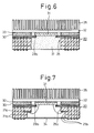
- Fig. 6 shows another embodiment of a semiconductor-device package of this invention.
- the cap 34 is not used to air-tightly seal the bottom surface of the chip-accommodating hole 25, but the chip-accommodating hole 25 is filled with a resin 37 to hermetically seal the chip 31 and the TAB tape.
- the chip accommodating holes 25b of the printed circuit boards 21b are larger than the chip accommodating holes 25a of the printed circuit boards 21a.
- chip 31 is electrically connected to the conductive patterns 39 on the circuit board 21a by bonding wires 41. Such a connection can be done by a conventional wire-bonding process.
- Fig. 8 shows another embodiment of a semiconductor-device package which is similar to that of Fig. 7, except that the cap 34 is not used, but the chip-accommodating hole 25a, 25b is filled with a resin 37 in the same manner as the embodiment of Fig. 6.
- Fig. 9 shows another embodiment of a semiconductor-device package which is similar to that of Fig. 6, except that the heat sink 32 and the fin member 35 are not used. Therefore, the structure and the function of this embodiment are quite the same as the embodiment of Fig. 6 except for the heat radiation means.
- a semiconductor-device package of this invention it is possible to bond a semiconductor device package and a chip together by a conventional TAB bonding technique in order to electrically couple the package and the chip together.
- a semiconductor-device package of the present invention is especially suitable for packaging a multi-pin and narrow-pitch chip which cannot be bonded by a conventional wire-bonding technique.
- the present invention can provide a miniature and low-cost semiconductor-device package which has excellent packaging ability because the semiconductor-device package of the present invention has no outer leads projecting outward in contrast to a TAB tape.
- the present invention it becomes possible to provide a semiconductor-device which excels in heat radiating ability, high-density packaging ability and electrical properties even when it mounts a multi-pin, narrow-pitch, high-speed and high-power chip.
Abstract
Description
- The present invention relates to a semiconductor-device package and a semiconductor device.
- A TAB (Tab Automated Bonding) tape comprises a heat resistant support film (for example, a polyimide film or the like) and a circuit pattern made of copper foil formed on the support film, the circuit pattern having inner leads projecting inside an element-accommodating hole of the support film and outer leads projecting outside the support film.
- A conventional bonding technique using this TAB tape makes it possible to facilitate tests of semiconductor elements (chips) before packaging them, to simultaneously bond a narrow-pitch chip whose pitch width is so narrow that this chip cannot be simultaneously bonded by means of a conventional multi-pin and wire-bonding technique. Furthermore such a TAB tape bonding technique is superior to wire-bonding technique with regard to its high frequency properties and is suitable to high density packaging. Therefore, such a TAB tape bonding technique is very appropriate to a multi-pin, narrow-pitch and high-speed chip, such as a CPU chip or the like.
- However, in such a conventional TAB tape bonding technique, both inner lead bonding and outer lead bonding is required and, as a result, a large number of working man-hours are inevitably required. In addition to this, because of requirements for mounting the package on a substrate, the pitch width between outer leads cannot be made narrow in the same manner as the pitch width between inner leads and, for this reason, the outer leads must project beyond its support film. Thus, according to such a conventional TAB tape bonding technique, the overall size of a semiconductor device typically becomes larger when a chip is mounted on it, which is contrary to demands of miniaturization.
- Furthermore, when such a conventional TAB tape bonding technique is applied to a high-power chip such as a CPU chip or the like, complex and expensive packaging is necessary because adaptation to a heat radiating structure is difficult to obtain.
- According to this invention a semiconductor device package comprises a printed circuit board having a chip-accommodating hole, respective surfaces and a circuit pattern, one of said surfaces being provided with external connection terminals electrically connected to said circuit pattern;
a flexible substrate comprising a supporting film having a central hole substantially in alignment with said chip-accommodating hole and a circuit pattern formed on said supporting film, at least a part of said circuit pattern projecting inside said central hole as inner leads having micro patterns; and
said flexible substrate being bonded to the other surface of said printed circuit board in such a manner that the circuit pattern of the flexible substrate is electrically connected to the circuit pattern of said printed circuit board. - Preferably a semiconductor-device comprises: a package in accordance with the invention, and a semiconductor chip bonded and mounted on said inner leads of said package, and sealing means for sealing said semiconductor chip located in said chip accommodating hole.
- Preferably the semiconductor device also includes a heat radiating plate attached to said package so as to cover said chip-accommodating hole and directly or indirectly contact said semiconductor chip to support it.
- According to a semiconductor-device package of this invention, it is possible to perform bonding by a conventional bonding technique in order to electrically connect said semiconductor-device package and a chip together. Thus a semiconductor-device package of the present invention is especially suitable for packaging a multi-pin and narrow-pitch chip which cannot be bonded by a conventional wire-bonding technique. Furthermore, the present invention can provide a miniature and low-cost semiconductor-device package which has excellent packaging ability because the semiconductor-device package of the present invention has no outer leads projecting outward in contrast to a TAB tape.
- Furthermore, according to a semiconductor device of the present invention, it becomes possible to provide a semiconductor device which excels in heat radiating ability, high-density packaging ability and electrical properties even when it mounts a multi-pin, narrow-pitch and high-power chip.
- Particular embodiments in accordance with this invention will now be described and contrasted with the prior art with reference to the accompanying drawings; in which;
- Figure 1 is a vertical cross-sectional view of anembodiment of a semiconductor-device package according to the present invention;
- Figure 2 is a bottom view of the example of Fig. 1;
- Figure 3 is a longitudinal sectional view of the example of Fig. 1 which is completed as a semiconductor device.
- Figure 4 shows another example of the substrate in the embodiment shown in Fig. 1;
- Figure 5 shows another example of the heat sink in the embodiment shown in Fig. 1;
- Figure 6 is a cross-sectional view of another embodiment of a semiconductor-device package of this invention;
- Figure 7 is a cross-sectional view of another embodiment of a semiconductor-device package of this invention;
- Figure 8 is a cross-sectional view of another embodiment of a semiconductor-device package of this invention;
- Figure 9 is a cross-sectional view of an embodiment similar to that of Fig. 6; and
- Figure 10 is a cross-sectional view of a semiconductor device having a conventional heat-radiating structure.
- Figure. 10 shows an example of a heat radiation structure on a conventional semiconductor device.
- This conventional semiconductor device has complex and expensive package structure. As shown in this figure, a circuit pattern for a PGA (Pin Grid Array)
type package 10 and achip 11 are connected through aTAB tape 12 and are sealed by acap 13. Moreover, by means of soldering or the like, aheat sink 15 is fastened to asupport 14 bonded to thechip 11. - Fig. 1 is a cross-sectional view of an embodiment of a semiconductor-
device package 20 and Fig. 2 is a bottom view of the same. A multi-layer printed circuit board is indicated at 21. The top pattern and the bottom pattern of this printed circuit board are electrically coupled together through conducting portions as through-hole plating or the like. This printed circuit board has multiple layers which include a signal circuit pattern, as well as a ground circuit pattern, a power-supply circuit pattern and the like which are separated from the signal layer in view of these electrical properties. These circuit patterns are formed inside the printed circuit board. - External connection bumps or
terminals 24 are formed on the bottom surface of the printedcircuit board 21. Thesebumps 24 may be lead pins, solderable pads or conductive adhesive. - A chip-accommodating
hole 25 is formed in the centre portion of the printedcircuit board 21. - The printed
circuit board 21 is provided on the bottom surface thereof with a dent along the periphery of the chip-accommodatinghole 25. This dent works as a recess for a cap fitting. - A flexible substrate is indicated at 26. This substrate is fixed on the upper surface of the printed
circuit board 21 by means of an adhesive. In the embodiment shown in Fig. 1, by etching a copper foil on the bottom surface of the supporting film 27 (for example, a polyimide film), acircuit pattern 28a on a bottom surface of the supportingfilm 27 and a pattern ofinner leads 28b projecting inside said chip-accommodatinghole 25 are formed. - The supporting
film 27 is also formed in a frame-like form which has a hole in its centre portion. This hole is made so as to have a smaller size than that of the chip-accommodatinghole 25. Preferably, a portion of the supportingfilm 27 projects inside thechip accommodating hole 25 and supports the base portions of theinner leads 28b which project inside thechip accommodating hole 25. - As described above, the
flexible substrate 26 is fixed on the printedcircuit board 29 by means of an adhesive. - In the same way as an electrical connection between the lower and upper patterns in a conventional printed circuit board, a circuit pattern on the upper surface of the printed
circuit board 21 and thecircuit pattern 28a on the bottom surface of the supportingfilm 27 are electrically coupled together through a plated film on the inner surface of through-holes. - This plated film is formed by boring holes through the printed circuit board at necessary points and by forming a through-hole plated film on the inner surface of the through-holes. That is to say, the whole structure of a
package body 20 is able to be made by means of a substantially same structure and method as those used for a conventional printed circuit board. Furthermore, according to this embodiment, only the inner leads 28b of the circuit pattern on the top layer of the printed circuit board project inside thechip accommodating hole 25 in the form of TAB tape. This makes the structure of thepackage 20 different from that of a conventional semiconductor-device package. - It is preferable to bond a
spacer 30 made of a material such as a resin containing a glass-filler to the upper side of the supportingfilm 27 by using an adhesive material. Preferably, thisspacer 30 has such a thickness that the upper surface of a semiconductor chip 31 (Fig. 3) can be flush with the upper surface of thespacer 30 when thesemiconductor chip 31 is mounted on theinner leads 28b. - Fig. 3 shows an embodiment of a semiconductor device in which the
semiconductor chip 31 is mounted and sealed on the above-mentionedpackage 20. - The
chip 31 can be mounted on theinner leads 28b by simultaneous bonding. The upper surface of thechip 31 mounted in this manner is almost flush with the upper surface of thespacer 30. The upper side of thechip 31 and the upper side of thespacer 30 are applied with an adhesive 33 and aheat sink 32 is fixed on these surfaces and is laid over the chip-accommodatinghole 25. - The
heat sink 32 may be made of a metal material such as aluminum, copper-tungsten alloy, copper and the like. Afin member 35 is preferably mounted on theheat sink 32. - Then, after the bottom surface of the chip-accommodating
hole 25 is air-tightly sealed by acap 34, a semiconductor device is completed. - Furthermore, each of the upper and bottom surfaces of the
inner leads 28b can be provided with the above mentioned supporting film 27 (Fig. 4) and, as a result, the inner leads 28b can be supported from their both the upper and bottom surfaces, which reinforces the mechanical strength of the inner leads. In this case, by the formation of through-holes piecing the printedcircuit board 21, the electrical coupling between thecircuit pattern 28a and the circuit pattern on the upper side of the printedcircuit board 21 can be established in the same manner as described above. - Furthermore, it is not always necessary to use the
spacer 30. When thespacer 30 is not used, it is preferable to use theheat sink 32 having a recess whose depth is equal to the thickness of thechip 31, as shown in Fig. 5. - Fig. 6 shows another embodiment of a semiconductor-device package of this invention. In this embodiment, the
cap 34 is not used to air-tightly seal the bottom surface of the chip-accommodatinghole 25, but the chip-accommodatinghole 25 is filled with aresin 37 to hermetically seal thechip 31 and the TAB tape. - In an embodiment shown in Fig. 7, the
chip accommodating holes 25b of the printedcircuit boards 21b are larger than thechip accommodating holes 25a of the printedcircuit boards 21a. Thus,chip 31 is electrically connected to the conductive patterns 39 on thecircuit board 21a by bonding wires 41. Such a connection can be done by a conventional wire-bonding process. - Fig. 8 shows another embodiment of a semiconductor-device package which is similar to that of Fig. 7, except that the
cap 34 is not used, but the chip-accommodatinghole resin 37 in the same manner as the embodiment of Fig. 6. - Fig. 9 shows another embodiment of a semiconductor-device package which is similar to that of Fig. 6, except that the
heat sink 32 and thefin member 35 are not used. Therefore, the structure and the function of this embodiment are quite the same as the embodiment of Fig. 6 except for the heat radiation means. - According to a semiconductor-device package of this invention, it is possible to bond a semiconductor device package and a chip together by a conventional TAB bonding technique in order to electrically couple the package and the chip together. Thus a semiconductor-device package of the present invention is especially suitable for packaging a multi-pin and narrow-pitch chip which cannot be bonded by a conventional wire-bonding technique. Furthermore, the present invention can provide a miniature and low-cost semiconductor-device package which has excellent packaging ability because the semiconductor-device package of the present invention has no outer leads projecting outward in contrast to a TAB tape.
- According to the present invention, it becomes possible to provide a semiconductor-device which excels in heat radiating ability, high-density packaging ability and electrical properties even when it mounts a multi-pin, narrow-pitch, high-speed and high-power chip.
Claims (7)
- A semiconductor-device package (20) comprising:
a printed circuit board (21) having a chip-accommodating hole (25), respective surfaces and a circuit pattern, one of said surfaces being provided with external connection terminals (24) electrically connected to said circuit pattern;
a flexible substrate (26) comprising a supporting film (27) having a central hole substantially in alignment with said chip-accommodating hole (25) and a circuit pattern (28) formed on said supporting film (27), at least a part of said circuit pattern (28) projecting inside said central hole as inner leads (28b) having micro patterns; and,
said flexible substrate (26) being bonded to the other surface of said printed circuit board (21) in such a manner that the circuit pattern (28) of the flexible substrate (26) is electrically connected to the circuit pattern of said printed circuit board (21). - A semiconductor-device package according to claim 1, wherein said printed circuit board (21) is multi-layer printed circuit board.
- A semiconductor device comprising:
a package (20) in accordance with claim 1 or 2;
a semiconductor chip (31) bonded and mounted on said inner leads (28b) of said package (20); and,
sealing means (34, 37) for sealing said semiconductor chip (31) located in said chip accommodating hole (25). - A semiconductor-device according to claim 3, which also includes:
a heat radiating plate. (32) attached to said package (20) so as to cover said chip-accommodating hole (25) and directly or indirectly contact said semiconductor chip (31) to support it. - A semiconductor-device according to claim 4, wherein said heat radiating plate (32) is attached to said package (20) via a spacer (30).
- A semiconductor-device according to claim 4 or 5, wherein said sealing means includes a cap (34) which hermetically closes said chip-accommodating hole (25) in cooperation with said heat radiating plate (32).
- A semiconductor-device according to claim 3, 4 or 5, wherein said sealing means is a moulded resin (37) filling said chip-accommodating hole (25).
Applications Claiming Priority (2)
| Application Number | Priority Date | Filing Date | Title |
|---|---|---|---|
| JP5063737A JPH06275677A (en) | 1993-03-23 | 1993-03-23 | Package for semiconductor device and semiconductor device |
| JP63737/93 | 1993-03-23 |
Publications (2)
| Publication Number | Publication Date |
|---|---|
| EP0617465A1 true EP0617465A1 (en) | 1994-09-28 |
| EP0617465B1 EP0617465B1 (en) | 1998-11-04 |
Family
ID=13238028
Family Applications (1)
| Application Number | Title | Priority Date | Filing Date |
|---|---|---|---|
| EP94302013A Expired - Lifetime EP0617465B1 (en) | 1993-03-23 | 1994-03-22 | A semiconductor device and package |
Country Status (5)
| Country | Link |
|---|---|
| US (1) | US5404273A (en) |
| EP (1) | EP0617465B1 (en) |
| JP (1) | JPH06275677A (en) |
| KR (1) | KR0135585B1 (en) |
| DE (1) | DE69414291T2 (en) |
Cited By (9)
| Publication number | Priority date | Publication date | Assignee | Title |
|---|---|---|---|---|
| EP0718882A1 (en) * | 1993-09-03 | 1996-06-26 | Advanced Semiconductor Assembly Technology, Inc. | Tab grid array for a semiconductor device |
| EP0701278A3 (en) * | 1994-09-08 | 1997-03-26 | Shinko Electric Ind Co | Semiconductor device and method for manufacturing same |
| FR2747509A1 (en) * | 1996-04-12 | 1997-10-17 | Nec Corp | Semiconductor integrated circuit mounting assembly |
| EP0817266A2 (en) * | 1996-07-01 | 1998-01-07 | NEC Corporation | Mounting structure for an integrated circuit |
| WO2001094874A1 (en) * | 2000-06-07 | 2001-12-13 | Siemens Aktiengesellschaft | Firing component for activating an occupant protection means of a motor vehicle |
| WO2002073690A2 (en) * | 2001-03-07 | 2002-09-19 | Teledyne Technologies Incorporated | A method of packaging a device with a lead frame |
| US7656236B2 (en) | 2007-05-15 | 2010-02-02 | Teledyne Wireless, Llc | Noise canceling technique for frequency synthesizer |
| US8179045B2 (en) | 2008-04-22 | 2012-05-15 | Teledyne Wireless, Llc | Slow wave structure having offset projections comprised of a metal-dielectric composite stack |
| US9202660B2 (en) | 2013-03-13 | 2015-12-01 | Teledyne Wireless, Llc | Asymmetrical slow wave structures to eliminate backward wave oscillations in wideband traveling wave tubes |
Families Citing this family (30)
| Publication number | Priority date | Publication date | Assignee | Title |
|---|---|---|---|---|
| US5854534A (en) | 1992-08-05 | 1998-12-29 | Fujitsu Limited | Controlled impedence interposer substrate |
| JPH0831988A (en) * | 1994-07-20 | 1996-02-02 | Nec Corp | Sealing structure of tape carrier package |
| JPH0846085A (en) * | 1994-08-02 | 1996-02-16 | Fujitsu Ltd | Semiconductor device and method of manufacture |
| EP0698922B1 (en) * | 1994-08-12 | 2001-06-06 | STMicroelectronics S.r.l. | Leadframe for supporting integrated semiconductor devices |
| KR0170023B1 (en) * | 1994-12-16 | 1999-02-01 | 황인길 | Semiconductor package |
| US5972736A (en) * | 1994-12-21 | 1999-10-26 | Sun Microsystems, Inc. | Integrated circuit package and method |
| JP2636777B2 (en) * | 1995-02-14 | 1997-07-30 | 日本電気株式会社 | Semiconductor module for microprocessor |
| AU6450096A (en) * | 1995-07-14 | 1997-02-18 | Olin Corporation | Metal ball grid electronic package |
| WO1997044821A1 (en) * | 1996-05-22 | 1997-11-27 | Olin Corporation | Metal electronic package with peripherally attached leads |
| US5726079A (en) * | 1996-06-19 | 1998-03-10 | International Business Machines Corporation | Thermally enhanced flip chip package and method of forming |
| USRE39426E1 (en) | 1996-06-19 | 2006-12-12 | International Business Machines Corporation | Thermally enhanced flip chip package and method of forming |
| US5724230A (en) * | 1996-06-21 | 1998-03-03 | International Business Machines Corporation | Flexible laminate module including spacers embedded in an adhesive |
| US5812376A (en) * | 1997-04-21 | 1998-09-22 | Chrysler Corporation | Mounting assembly for electrical components and heat sinks |
| TW449844B (en) * | 1997-05-17 | 2001-08-11 | Hyundai Electronics Ind | Ball grid array package having an integrated circuit chip |
| US6552264B2 (en) | 1998-03-11 | 2003-04-22 | International Business Machines Corporation | High performance chip packaging and method |
| JP2000114413A (en) * | 1998-09-29 | 2000-04-21 | Sony Corp | Semiconductor device, its manufacture, and method for mounting parts |
| TW399309B (en) * | 1998-09-30 | 2000-07-21 | World Wiser Electronics Inc | Cavity-down package structure with thermal via |
| JP3269815B2 (en) * | 1999-12-13 | 2002-04-02 | 富士通株式会社 | Semiconductor device and manufacturing method thereof |
| US6350954B1 (en) | 2000-01-24 | 2002-02-26 | Motorola Inc. | Electronic device package, and method |
| US6469907B1 (en) | 2000-10-23 | 2002-10-22 | Team Pacific, Corporation | Packaging for power and other circuitry |
| JP2002134650A (en) * | 2000-10-23 | 2002-05-10 | Rohm Co Ltd | Semiconductor device and its manufacturing method |
| US6653167B2 (en) * | 2001-09-10 | 2003-11-25 | Sun Microsystems, Inc. | Facilitating heat transfer from an integrated circuit package |
| US6784540B2 (en) * | 2001-10-10 | 2004-08-31 | International Rectifier Corp. | Semiconductor device package with improved cooling |
| US6933603B2 (en) * | 2002-07-11 | 2005-08-23 | Teledyne Technologies Incorporated | Multi-substrate layer semiconductor packages and method for making same |
| JP3858834B2 (en) * | 2003-02-24 | 2006-12-20 | オンキヨー株式会社 | Semiconductor element heatsink |
| JP2010267954A (en) * | 2009-04-15 | 2010-11-25 | Panasonic Corp | Electronic device |
| FR3037439A1 (en) * | 2015-06-12 | 2016-12-16 | St Microelectronics Sa | ELECTRONIC DEVICE WITH REAR PLATE EVIDED. |
| DE102015115271B4 (en) * | 2015-09-10 | 2021-07-15 | Infineon Technologies Ag | ELECTRONICS ASSEMBLY WITH SUPPRESSION CAPACITORS AND METHOD FOR OPERATING THE ELECTRONICS ASSEMBLY |
| US10008411B2 (en) | 2016-12-15 | 2018-06-26 | Infineon Technologies Ag | Parallel plate waveguide for power circuits |
| US10410952B2 (en) | 2016-12-15 | 2019-09-10 | Infineon Technologies Ag | Power semiconductor packages having a substrate with two or more metal layers and one or more polymer-based insulating layers for separating the metal layers |
Citations (4)
| Publication number | Priority date | Publication date | Assignee | Title |
|---|---|---|---|---|
| EP0352429A2 (en) * | 1988-07-25 | 1990-01-31 | International Business Machines Corporation | High power, pluggable tape automated bonding package |
| EP0376062A1 (en) * | 1988-12-27 | 1990-07-04 | Eta SA Fabriques d'Ebauches | Electronic module with an integrated circuit for a portable object of small dimensions, such as a card or a key, and process for manufacturing such a module |
| EP0476971A2 (en) * | 1990-09-18 | 1992-03-25 | Ngk Insulators, Ltd. | Ceramic packages and ceramic wiring board |
| EP0524761A1 (en) * | 1991-07-22 | 1993-01-27 | AT&T Corp. | Plastic pin grid array package |
Family Cites Families (3)
| Publication number | Priority date | Publication date | Assignee | Title |
|---|---|---|---|---|
| US4964019A (en) * | 1989-12-27 | 1990-10-16 | Ag Communication Systems Corporation | Multilayer bonding and cooling of integrated circuit devices |
| JPH0496257A (en) * | 1990-08-03 | 1992-03-27 | Hitachi Ltd | Pin grid array type semiconductor integrated circuit device |
| JP3000307B2 (en) * | 1991-08-28 | 2000-01-17 | 株式会社日立製作所 | Semiconductor device with cooling device and method of manufacturing the same |
-
1993
- 1993-03-23 JP JP5063737A patent/JPH06275677A/en active Pending
-
1994
- 1994-03-22 DE DE69414291T patent/DE69414291T2/en not_active Expired - Fee Related
- 1994-03-22 KR KR1019940005728A patent/KR0135585B1/en not_active IP Right Cessation
- 1994-03-22 EP EP94302013A patent/EP0617465B1/en not_active Expired - Lifetime
- 1994-03-23 US US08/216,323 patent/US5404273A/en not_active Expired - Lifetime
Patent Citations (4)
| Publication number | Priority date | Publication date | Assignee | Title |
|---|---|---|---|---|
| EP0352429A2 (en) * | 1988-07-25 | 1990-01-31 | International Business Machines Corporation | High power, pluggable tape automated bonding package |
| EP0376062A1 (en) * | 1988-12-27 | 1990-07-04 | Eta SA Fabriques d'Ebauches | Electronic module with an integrated circuit for a portable object of small dimensions, such as a card or a key, and process for manufacturing such a module |
| EP0476971A2 (en) * | 1990-09-18 | 1992-03-25 | Ngk Insulators, Ltd. | Ceramic packages and ceramic wiring board |
| EP0524761A1 (en) * | 1991-07-22 | 1993-01-27 | AT&T Corp. | Plastic pin grid array package |
Non-Patent Citations (1)
| Title |
|---|
| "tape automated bonding/pin grid array package", IBM TECHNICAL DISCLOSURE BULLETIN, vol. 31, no. 4, September 1988 (1988-09-01), NEW YORK, pages 279 - 280 * |
Cited By (12)
| Publication number | Priority date | Publication date | Assignee | Title |
|---|---|---|---|---|
| EP0718882A1 (en) * | 1993-09-03 | 1996-06-26 | Advanced Semiconductor Assembly Technology, Inc. | Tab grid array for a semiconductor device |
| EP0701278A3 (en) * | 1994-09-08 | 1997-03-26 | Shinko Electric Ind Co | Semiconductor device and method for manufacturing same |
| FR2747509A1 (en) * | 1996-04-12 | 1997-10-17 | Nec Corp | Semiconductor integrated circuit mounting assembly |
| EP0817266A2 (en) * | 1996-07-01 | 1998-01-07 | NEC Corporation | Mounting structure for an integrated circuit |
| EP0817266A3 (en) * | 1996-07-01 | 1998-11-25 | NEC Corporation | Mounting structure for an integrated circuit |
| WO2001094874A1 (en) * | 2000-06-07 | 2001-12-13 | Siemens Aktiengesellschaft | Firing component for activating an occupant protection means of a motor vehicle |
| WO2002073690A2 (en) * | 2001-03-07 | 2002-09-19 | Teledyne Technologies Incorporated | A method of packaging a device with a lead frame |
| WO2002073690A3 (en) * | 2001-03-07 | 2003-05-15 | Teledyne Tech Inc | A method of packaging a device with a lead frame |
| US6828663B2 (en) | 2001-03-07 | 2004-12-07 | Teledyne Technologies Incorporated | Method of packaging a device with a lead frame, and an apparatus formed therefrom |
| US7656236B2 (en) | 2007-05-15 | 2010-02-02 | Teledyne Wireless, Llc | Noise canceling technique for frequency synthesizer |
| US8179045B2 (en) | 2008-04-22 | 2012-05-15 | Teledyne Wireless, Llc | Slow wave structure having offset projections comprised of a metal-dielectric composite stack |
| US9202660B2 (en) | 2013-03-13 | 2015-12-01 | Teledyne Wireless, Llc | Asymmetrical slow wave structures to eliminate backward wave oscillations in wideband traveling wave tubes |
Also Published As
| Publication number | Publication date |
|---|---|
| EP0617465B1 (en) | 1998-11-04 |
| DE69414291D1 (en) | 1998-12-10 |
| JPH06275677A (en) | 1994-09-30 |
| DE69414291T2 (en) | 1999-03-25 |
| KR0135585B1 (en) | 1998-04-22 |
| US5404273A (en) | 1995-04-04 |
| KR940022812A (en) | 1994-10-21 |
Similar Documents
| Publication | Publication Date | Title |
|---|---|---|
| US5404273A (en) | Semiconductor-device package and semiconductor device | |
| EP0638931B1 (en) | Multi-chip module | |
| US5677575A (en) | Semiconductor package having semiconductor chip mounted on board in face-down relation | |
| US6908794B1 (en) | Method of making a semiconductor package device that includes a conductive trace with recessed and non-recessed portions | |
| US6545366B2 (en) | Multiple chip package semiconductor device | |
| JP3209320B2 (en) | Multi-chip module package | |
| US7564137B2 (en) | Stackable integrated circuit structures and systems devices and methods related thereto | |
| US5684330A (en) | Chip-sized package having metal circuit substrate | |
| US5849608A (en) | Semiconductor chip package | |
| US5177863A (en) | Method of forming integrated leadouts for a chip carrier | |
| EP1189273A2 (en) | Semiconductor device and production process | |
| JPH081936B2 (en) | Chip carrier and method of manufacturing the same | |
| US6486551B1 (en) | Wired board and method of producing the same | |
| US5107329A (en) | Pin-grid array semiconductor device | |
| KR100226335B1 (en) | Molded plastic packaging of electronic devices | |
| US6989295B1 (en) | Method of making a semiconductor package device that includes an insulative housing with first and second housing portions | |
| KR19990069447A (en) | Semiconductor package and manufacturing method | |
| US6320250B1 (en) | Semiconductor package and process for manufacturing the same | |
| JPH0558657B2 (en) | ||
| JP3061014B2 (en) | Semiconductor device and manufacturing method thereof | |
| JPS6110299A (en) | Integrated circuit mounting structure | |
| KR100565766B1 (en) | Semiconductor chip package and manufacturing method the same | |
| KR100260996B1 (en) | Array type semiconductor package using a lead frame and its manufacturing method | |
| KR19980043249A (en) | Chip Scale Package with Grooved Printed Circuit Board | |
| JPH04139737A (en) | Method for mounting semiconductor chip |
Legal Events
| Date | Code | Title | Description |
|---|---|---|---|
| PUAI | Public reference made under article 153(3) epc to a published international application that has entered the european phase |
Free format text: ORIGINAL CODE: 0009012 |
|
| AK | Designated contracting states |
Kind code of ref document: A1 Designated state(s): DE FR GB |
|
| 17P | Request for examination filed |
Effective date: 19950324 |
|
| 17Q | First examination report despatched |
Effective date: 19970509 |
|
| GRAG | Despatch of communication of intention to grant |
Free format text: ORIGINAL CODE: EPIDOS AGRA |
|
| GRAG | Despatch of communication of intention to grant |
Free format text: ORIGINAL CODE: EPIDOS AGRA |
|
| GRAH | Despatch of communication of intention to grant a patent |
Free format text: ORIGINAL CODE: EPIDOS IGRA |
|
| GRAH | Despatch of communication of intention to grant a patent |
Free format text: ORIGINAL CODE: EPIDOS IGRA |
|
| GRAA | (expected) grant |
Free format text: ORIGINAL CODE: 0009210 |
|
| AK | Designated contracting states |
Kind code of ref document: B1 Designated state(s): DE FR GB |
|
| REF | Corresponds to: |
Ref document number: 69414291 Country of ref document: DE Date of ref document: 19981210 |
|
| ET | Fr: translation filed | ||
| PLBE | No opposition filed within time limit |
Free format text: ORIGINAL CODE: 0009261 |
|
| STAA | Information on the status of an ep patent application or granted ep patent |
Free format text: STATUS: NO OPPOSITION FILED WITHIN TIME LIMIT |
|
| 26N | No opposition filed | ||
| REG | Reference to a national code |
Ref country code: GB Ref legal event code: IF02 |
|
| PGFP | Annual fee paid to national office [announced via postgrant information from national office to epo] |
Ref country code: DE Payment date: 20070315 Year of fee payment: 14 |
|
| PGFP | Annual fee paid to national office [announced via postgrant information from national office to epo] |
Ref country code: GB Payment date: 20070321 Year of fee payment: 14 |
|
| PGFP | Annual fee paid to national office [announced via postgrant information from national office to epo] |
Ref country code: FR Payment date: 20070308 Year of fee payment: 14 |
|
| GBPC | Gb: european patent ceased through non-payment of renewal fee |
Effective date: 20080322 |
|
| REG | Reference to a national code |
Ref country code: FR Ref legal event code: ST Effective date: 20081125 |
|
| PG25 | Lapsed in a contracting state [announced via postgrant information from national office to epo] |
Ref country code: DE Free format text: LAPSE BECAUSE OF NON-PAYMENT OF DUE FEES Effective date: 20081001 |
|
| PG25 | Lapsed in a contracting state [announced via postgrant information from national office to epo] |
Ref country code: FR Free format text: LAPSE BECAUSE OF NON-PAYMENT OF DUE FEES Effective date: 20080331 |
|
| PG25 | Lapsed in a contracting state [announced via postgrant information from national office to epo] |
Ref country code: GB Free format text: LAPSE BECAUSE OF NON-PAYMENT OF DUE FEES Effective date: 20080322 |