EP0635744B1 - Optical system for light emitting diodes - Google Patents
Optical system for light emitting diodes Download PDFInfo
- Publication number
- EP0635744B1 EP0635744B1 EP93202869A EP93202869A EP0635744B1 EP 0635744 B1 EP0635744 B1 EP 0635744B1 EP 93202869 A EP93202869 A EP 93202869A EP 93202869 A EP93202869 A EP 93202869A EP 0635744 B1 EP0635744 B1 EP 0635744B1
- Authority
- EP
- European Patent Office
- Prior art keywords
- lens
- longitudinal
- optical system
- diode
- lens element
- Prior art date
- Legal status (The legal status is an assumption and is not a legal conclusion. Google has not performed a legal analysis and makes no representation as to the accuracy of the status listed.)
- Expired - Lifetime
Links
Images


Classifications
-
- H—ELECTRICITY
- H01—ELECTRIC ELEMENTS
- H01L—SEMICONDUCTOR DEVICES NOT COVERED BY CLASS H10
- H01L33/00—Semiconductor devices with at least one potential-jump barrier or surface barrier specially adapted for light emission; Processes or apparatus specially adapted for the manufacture or treatment thereof or of parts thereof; Details thereof
- H01L33/48—Semiconductor devices with at least one potential-jump barrier or surface barrier specially adapted for light emission; Processes or apparatus specially adapted for the manufacture or treatment thereof or of parts thereof; Details thereof characterised by the semiconductor body packages
- H01L33/52—Encapsulations
- H01L33/54—Encapsulations having a particular shape
-
- G—PHYSICS
- G02—OPTICS
- G02B—OPTICAL ELEMENTS, SYSTEMS OR APPARATUS
- G02B19/00—Condensers, e.g. light collectors or similar non-imaging optics
- G02B19/0004—Condensers, e.g. light collectors or similar non-imaging optics characterised by the optical means employed
- G02B19/0028—Condensers, e.g. light collectors or similar non-imaging optics characterised by the optical means employed refractive and reflective surfaces, e.g. non-imaging catadioptric systems
-
- G—PHYSICS
- G02—OPTICS
- G02B—OPTICAL ELEMENTS, SYSTEMS OR APPARATUS
- G02B19/00—Condensers, e.g. light collectors or similar non-imaging optics
- G02B19/0033—Condensers, e.g. light collectors or similar non-imaging optics characterised by the use
- G02B19/0047—Condensers, e.g. light collectors or similar non-imaging optics characterised by the use for use with a light source
- G02B19/0061—Condensers, e.g. light collectors or similar non-imaging optics characterised by the use for use with a light source the light source comprising a LED
-
- G—PHYSICS
- G02—OPTICS
- G02B—OPTICAL ELEMENTS, SYSTEMS OR APPARATUS
- G02B6/00—Light guides; Structural details of arrangements comprising light guides and other optical elements, e.g. couplings
- G02B6/0001—Light guides; Structural details of arrangements comprising light guides and other optical elements, e.g. couplings specially adapted for lighting devices or systems
-
- H—ELECTRICITY
- H01—ELECTRIC ELEMENTS
- H01L—SEMICONDUCTOR DEVICES NOT COVERED BY CLASS H10
- H01L33/00—Semiconductor devices with at least one potential-jump barrier or surface barrier specially adapted for light emission; Processes or apparatus specially adapted for the manufacture or treatment thereof or of parts thereof; Details thereof
- H01L33/48—Semiconductor devices with at least one potential-jump barrier or surface barrier specially adapted for light emission; Processes or apparatus specially adapted for the manufacture or treatment thereof or of parts thereof; Details thereof characterised by the semiconductor body packages
- H01L33/58—Optical field-shaping elements
-
- F—MECHANICAL ENGINEERING; LIGHTING; HEATING; WEAPONS; BLASTING
- F21—LIGHTING
- F21V—FUNCTIONAL FEATURES OR DETAILS OF LIGHTING DEVICES OR SYSTEMS THEREOF; STRUCTURAL COMBINATIONS OF LIGHTING DEVICES WITH OTHER ARTICLES, NOT OTHERWISE PROVIDED FOR
- F21V7/00—Reflectors for light sources
- F21V7/0091—Reflectors for light sources using total internal reflection
-
- F—MECHANICAL ENGINEERING; LIGHTING; HEATING; WEAPONS; BLASTING
- F21—LIGHTING
- F21Y—INDEXING SCHEME ASSOCIATED WITH SUBCLASSES F21K, F21L, F21S and F21V, RELATING TO THE FORM OR THE KIND OF THE LIGHT SOURCES OR OF THE COLOUR OF THE LIGHT EMITTED
- F21Y2115/00—Light-generating elements of semiconductor light sources
- F21Y2115/10—Light-emitting diodes [LED]
-
- H—ELECTRICITY
- H01—ELECTRIC ELEMENTS
- H01L—SEMICONDUCTOR DEVICES NOT COVERED BY CLASS H10
- H01L33/00—Semiconductor devices with at least one potential-jump barrier or surface barrier specially adapted for light emission; Processes or apparatus specially adapted for the manufacture or treatment thereof or of parts thereof; Details thereof
- H01L33/48—Semiconductor devices with at least one potential-jump barrier or surface barrier specially adapted for light emission; Processes or apparatus specially adapted for the manufacture or treatment thereof or of parts thereof; Details thereof characterised by the semiconductor body packages
- H01L33/58—Optical field-shaping elements
- H01L33/60—Reflective elements
Definitions
- This invention relates to an optical system for light emitting diodes.
- An optical system for light emitting diodes is known in which the diode, which acts as a light-emitting semiconductor element, is incorporated in a fixed manner on the optical axis of a carrier lens.
- the carrier lens consists of a front portion with an outer transverse surface formed concave towards the emitted light, and a longitudinal portion with an outer longitudinal surface, for incorporating the diode.
- US-A-4,698,730 and US-A-5,173,810 disclose optical systems according to the preamble of claim 1. This optical system has the drawback that the light rays are emitted with considerable dispersion, causing wastage of the emitted light energy and a consequent limitation in the performance of the optical system.
- This dispersion is also very influenced by the extent of the geometrical tolerances in positioning the LED relative to the carrier lens, which acts as a container and rigidifies the position of the constituent elements of the active part of the LED.
- These geometrical tolerances are practically inevitable with current LED production methods, because of which the optical systems are produced only in a few limited types without particular adaptation and personalization to the emitting element. Manufacturers are therefore compelled to apply a careful selection procedure to the LEDs produced, with substantial cost increase, in order to market homogeneous batches.
- DE-A-2,510,267 discloses a light-emitting unit, in which a diode is fixed in an inner lens element that is secured in a cavity by an intermediate lens element positioned between the inner lens element and a carrier lens element, and formed by in-situ polymerisation.
- the longitudinal part of the outer lens element is cylindrical and the inner element has a corresponding shape; this causes a problem in fitting the inner element in the outer element, since even in this case, the tolerances concerning size and shape of the inner element may be quite small.
- the object of the present invention is to provide an optical system which does not present said drawbacks and which enables high intensity to be achieved with only modest dispersion.
- This object is achieved according to the invention by an optical system for light emitting diodes, according to claim 1.
- This optical system of the present invention has the advantage that the performance of the optical system is considerably increased by the reduction in the light radiation dispersion by virtue of the outer longitudinal surface and the further transverse surface of the carrier lens according to the present invention. Moreover, the technical features of the present optical system lead to an easier mounting of the device and also allow a higher tolerance in size variation of the inner lens element.
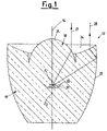
- an optical system for light emitting diodes comprises a carrier lens, indicated overall by 12, with a diode 13 incorporated in a fixed manner on the optical axis 14 within the carrier lens 12.
- a mirror 31 is positioned within the carrier lens 12 in such a manner that the light emitted by the diode 13 can be transmitted by the optical system only in a frontal direction.
- the carrier lens 12 consists of a front portion 18 with an outer transverse surface 25 formed concave towards the emitted light, and a longitudinal portion 19 for incorporating the diode 13 with the mirror 31.
- the longitudinal portion 19 is shaped such that its outer longitudinal surface 22 is concave towards the diode 13, in this case with its major diameter close to the front portion 18.
- the transverse surface 25 is surrounded by a further outer transverse surface 24 having a convex shape of spherical or ellipsoidal nature towards the light emitted in a longitudinal direction.
- the longitudinal portion 19 is able to reflect light rays emitted by the diode 13 via the concave longitudinal surface 22 towards the further outer transverse surface 24, which is able to transmit the light rays to the outside in a longitudinal direction.
- Figure 1 also shows a light ray 27 emitted by the diode 13 in a direction towards the outer transverse surface 25, at which it is refracted such that it leaves the carrier lens 12 in the longitudinal direction and hence parallel to the optical axis 14.
- the diode 13, together with the mirror 31, is able to emit light rays within a solid angle of 2 ⁇ about the optical axis 14, these being conveyed by the optical system formed by the surfaces 22, 24 and 25 into a beam of limited angular aperture.
- FIG. 2 shows an embodiment of the optical system according to the present invention, in which parts corresponding to the embodiment of Figure 1 are indicated by the same numerals.
- the carrier lens 12 consists of a plurality of lenses, namely an outer lens element 17, an inner lens 26 carrying the diode 13 with the mirror 31, and an intermediate lens 20.
- the outer lens element 17 has the same external configuration as the carrier lens 12 of the embodiment of Figure 1 and is provided internally with a cavity 21.
- the cavity 21 is bounded in a longitudinal direction by a front part 18 and in a direction perpendicular to the optical axis 14 by a longitudinal part 19.
- the cavity 21 is therefore open in a longitudinal direction in front of the front part 18 to allow the inner lens 26 to be inserted into the outer lens element 17.
- the inner lens 26 is integrated into the cavity 21 such that the intermediate lens 20 is positioned between the inner lens 26 and the lens element 17 and formed by in-situ polymerization of a suitable resin. In this manner the intermediate lens 20 fixes the inner lens 26 to the lens element 17 so that there are no gaps in the cavity 21.
- the inner lens 26 comprises in its front part a surface 15 concave towards the emitted light and at its longitudinal part a cylindrical or frusto-conical surface 16.
- the front part of the inner lens 26 is generally of hemispherical shape.
- the outer lens element 17 is shaped according to the present invention such that the front part 18 is in the form of the meniscus cup concave towards the emitted light.
- the longitudinal part 19 is shaped such that the cavity 21 is in the form of a cone frustum with its minor diameter towards the front part 18.
- Figure 2 also shows a light ray 29 emitted by the diode 13 and refracted at the two separation surfaces of the intermediate lens 20 in the direction of the outer transverse surface 25, at which it is refracted such that it emerges from the carrier lens 12 again in a longitudinal direction parallel to the optical axis 14,
- the lens element 17 is provided in the cavity 21 with a plurality of longitudinal guides 23, in this case three guides 23.
- the purpose of the guides 23, which on assembly are in contact with the outer diameter of the inner lens 26, is to position the inner lens 26 plus diode 13 in the cavity 21 such that the diode 13 is always on the optical axis 14.
- the carrier lens 12, the outer lens element 17, the intermediate lens 20 and the inner lens 26 are of injection-mouldable transparent polymer.
- the absolute refractive index of the intermediate lens 20 must be different from the absolute refractive index of the inner lens 26 and of the lens element 17.
- the absolute refractive index of the inner lens 26 is generally chosen by the manufacturer as high as possible (greater than 1.57) to improve the emissivity of the LED which has an index close to 3.
- the absolute refractive index of the intermediate lens 20 is between 1.33 and 1.48 and is preferably 1.415, and that of the lens element 17 is between 1.48 and 1.63, and is preferably 1.59.
- the complete optical system of the present invention is formed by firstly prefabricating the lens element 17 and the inner lens 26 with the diode 13 and mirror 31 incorporated.
- the inner lens 26 is then inserted into the cavity 21 of the lens element 17, in which the diode 13 is automatically positioned on the optical axis 14 because of the presence of the longitudinal guides 23.
- the free space remaining between the inner lens 26 and the lens element 17 is filled by pouring in a transparent thermosetting polymer, which forms the intermediate lens 20. In this manner the optical system 11 becomes a single piece by virtue of the intermediate lens 20.
- the improvement in the optical system according to the present invention is based on the fact that the longitudinal surface 22 and the transverse surface 24 of the longitudinal part 19 of the lens element 17 allow recovery of the light radiation which would otherwise be dispersed by the inability of the surface 16, for example cylindrical, of the inner lens 26 to produce adequate transmission.
- the optical system of the present invention is therefore a bifocal optical system, being structured such that the longitudinal part 19 has a focal point indicated by F2, which is different from that indicated by F1 of the front part 18.
- This focal difference is substantially equivalent to the error in the positioning of the diode 13 within the inner lens 26. It is noted that any reduction in the efficiency of the front part 18 caused by the LED positioning error is recovered by the longitudinal part 19, to increase the efficiency of the optical system, and vice versa. In this manner the achieved overall efficiency of the optical system is practically constant independently of the LED positioning error.
- the second embodiment of the optical system is therefore applied to existing commercial carrier lenses, which can have any absolute refractive index, and enables their performance to be considerably improved by levelling the varying degree of dispersion in commercial production. In this case the performance is improved on an average by a factor of between 1.5 and 4, depending on whether the initial intensity is high or low.
- a commercially existent carrier lens such as the inner lens 26 with the diode 13 and mirror 31 incorporated, is only effective for transmitting light rays to the outside in the longitudinal direction, these being emitted by the diode 13 in a bundle having an angular aperture of a maximum of 39° about the optical axis 14, as shown in Figure 4.
- the application of the optical system of the present invention enables light rays emitted by the diode 13 in a bundle having an angular aperture greater than 39°, for example 45° or more about the optical axis 14, to be transmitted to the outside in a longitudinal direction.
- the embodiment of Figure 2 has the further advantage that as the lens element of the present invention is of non-limiting form, the optical system can be easily applied to different types of light emitter device, for example the internal lens type, to always achieve a considerable improvement in the effective performance of the LED.
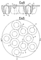
- Figures 3 to 6 show groups of lens elements 17, in which each group is formed as a single piece.
- Figures 3 and 4 show a group for example of five lens elements 17, whereas Figures 5 and 6 show a group of ten lens elements 17.
- the present invention is very suitable for example for use in variable-message road information panels and in motor vehicle indicators.
- the present invention is very effective, because if sunlight is present the light emitting diodes 13 must demonstrate maximum performance, which can be achieved only by the present optical system.
- Figure 7 shows a second embodiment of the outer lens element 17 with a flat transverse surface 24 and a paraboloid outer, longitudinal surface 22.
- Figure 8 shows a third embodiment of the outer lens element 17 with a transverse surface 24 of spherical or ellipsoidal rotation shape, the outer longitudinal surface 22 being ellipsoidal.
- the embodiment of the optical system according to the present invention therefore consists of two sub-systems, one being purely dioptric and the other being mixed dioptric-catoptric, in two different practical forms, one of which is homogeneous and to be used for incorporation of the LED 13 in the polymer,. and the other being additional employing more than one polymer, to be used to improve the performance of LED devices which are already commercially available.
- the outer longitudinal surface 22 can also be aluminized.
Abstract
Description
- This invention relates to an optical system for light emitting diodes.
- An optical system for light emitting diodes (LEDs) is known in which the diode, which acts as a light-emitting semiconductor element, is incorporated in a fixed manner on the optical axis of a carrier lens. The carrier lens consists of a front portion with an outer transverse surface formed concave towards the emitted light, and a longitudinal portion with an outer longitudinal surface, for incorporating the diode. For example, US-A-4,698,730 and US-A-5,173,810 disclose optical systems according to the preamble of
claim 1. This optical system has the drawback that the light rays are emitted with considerable dispersion, causing wastage of the emitted light energy and a consequent limitation in the performance of the optical system. This dispersion is also very influenced by the extent of the geometrical tolerances in positioning the LED relative to the carrier lens, which acts as a container and rigidifies the position of the constituent elements of the active part of the LED. These geometrical tolerances are practically inevitable with current LED production methods, because of which the optical systems are produced only in a few limited types without particular adaptation and personalization to the emitting element. Manufacturers are therefore compelled to apply a careful selection procedure to the LEDs produced, with substantial cost increase, in order to market homogeneous batches. - Moreover, in order to overcome these drawbacks DE-A-2,510,267 discloses a light-emitting unit, in which a diode is fixed in an inner lens element that is secured in a cavity by an intermediate lens element positioned between the inner lens element and a carrier lens element, and formed by in-situ polymerisation. However, the longitudinal part of the outer lens element is cylindrical and the inner element has a corresponding shape; this causes a problem in fitting the inner element in the outer element, since even in this case, the tolerances concerning size and shape of the inner element may be quite small.
- The object of the present invention is to provide an optical system which does not present said drawbacks and which enables high intensity to be achieved with only modest dispersion. This object is achieved according to the invention by an optical system for light emitting diodes, according to
claim 1. - This optical system of the present invention has the advantage that the performance of the optical system is considerably increased by the reduction in the light radiation dispersion by virtue of the outer longitudinal surface and the further transverse surface of the carrier lens according to the present invention. Moreover, the technical features of the present optical system lead to an easier mounting of the device and also allow a higher tolerance in size variation of the inner lens element.
- The technical characteristics and further advantages of the present invention will be more apparent from the description given hereinafter by way of non-limiting example with reference to the accompanying drawings, in which:
- Figure 1 is a longitudinal section through an embodiment of an optical system belonging to the state of the art;
- Figure 2 is a longitudinal section through an embodiment of an optical system according to the present invention;
- Figure 3 is a view from below of a group of five outer lens elements of the optical system of Figure 2;
- Figure 4 is a longitudinal section through the group of outer lens elements on the line IV-IV of Figure 3;
- Figure 5 is a view from below of a group of ten outer lens elements of the optical system of Figure 2;
- Figure 6 is a longitudinal section through the group of outer lens elements on the line VI-VI of Figure 5;
- Figure 7 is a longitudinal section through a second embodiment of the outer lens element of Figure 2; and
- Figure 8 is a longitudinal section through a third embodiment of the outer lens element of Figure 2.
-
- With reference to Figure 1, an optical system for light emitting diodes (LEDs) comprises a carrier lens, indicated overall by 12, with a
diode 13 incorporated in a fixed manner on theoptical axis 14 within thecarrier lens 12. Amirror 31 is positioned within thecarrier lens 12 in such a manner that the light emitted by thediode 13 can be transmitted by the optical system only in a frontal direction. Thecarrier lens 12 consists of afront portion 18 with an outertransverse surface 25 formed concave towards the emitted light, and alongitudinal portion 19 for incorporating thediode 13 with themirror 31. - The
longitudinal portion 19 is shaped such that its outerlongitudinal surface 22 is concave towards thediode 13, in this case with its major diameter close to thefront portion 18. Thetransverse surface 25 is surrounded by a further outertransverse surface 24 having a convex shape of spherical or ellipsoidal nature towards the light emitted in a longitudinal direction. - It can also be seen from Figure 1 that the further outer
transverse surface 24 surrounds thefront portion 18 of thecarrier lens 12 coaxially, and the outerlongitudinal surface 22 of thecarrier lens 12 is coaxial with theoptical axis 14. - By virtue of its outer configuration, the
longitudinal portion 19 is able to reflect light rays emitted by thediode 13 via the concavelongitudinal surface 22 towards the further outertransverse surface 24, which is able to transmit the light rays to the outside in a longitudinal direction. - Figure 1 also shows a
light ray 27 emitted by thediode 13 in a direction towards the outertransverse surface 25, at which it is refracted such that it leaves thecarrier lens 12 in the longitudinal direction and hence parallel to theoptical axis 14. - It also shows a
light ray 28 striking the outerlongitudinal surface 22, at which it is refracted to reach thetransverse surface 24, which refracts it in the longitudinal direction parallel to theoptical axis 14. - Hence the
diode 13, together with themirror 31, is able to emit light rays within a solid angle of 2π about theoptical axis 14, these being conveyed by the optical system formed by thesurfaces - Figure 2 shows an embodiment of the optical system according to the present invention, in which parts corresponding to the embodiment of Figure 1 are indicated by the same numerals.
- In this case the
carrier lens 12 consists of a plurality of lenses, namely anouter lens element 17, aninner lens 26 carrying thediode 13 with themirror 31, and anintermediate lens 20. Theouter lens element 17 has the same external configuration as thecarrier lens 12 of the embodiment of Figure 1 and is provided internally with acavity 21. Thecavity 21 is bounded in a longitudinal direction by afront part 18 and in a direction perpendicular to theoptical axis 14 by alongitudinal part 19. - The
cavity 21 is therefore open in a longitudinal direction in front of thefront part 18 to allow theinner lens 26 to be inserted into theouter lens element 17. - The
inner lens 26 is integrated into thecavity 21 such that theintermediate lens 20 is positioned between theinner lens 26 and thelens element 17 and formed by in-situ polymerization of a suitable resin. In this manner theintermediate lens 20 fixes theinner lens 26 to thelens element 17 so that there are no gaps in thecavity 21. - The
inner lens 26 comprises in its front part asurface 15 concave towards the emitted light and at its longitudinal part a cylindrical or frusto-conical surface 16. In this case the front part of theinner lens 26 is generally of hemispherical shape. - The
outer lens element 17 is shaped according to the present invention such that thefront part 18 is in the form of the meniscus cup concave towards the emitted light. Thelongitudinal part 19 is shaped such that thecavity 21 is in the form of a cone frustum with its minor diameter towards thefront part 18. - As an example of the operation of this embodiment of the optical system according to the present invention, Figure 2 also shows a
light ray 29 emitted by thediode 13 and refracted at the two separation surfaces of theintermediate lens 20 in the direction of the outertransverse surface 25, at which it is refracted such that it emerges from thecarrier lens 12 again in a longitudinal direction parallel to theoptical axis 14, - It also shows a
light ray 30 which strikes the outerlongitudinal surface 22, at which it is refracted to reach thetransverse surface 24, where it is refracted in a longitudinal direction parallel to theoptical axis 14. As can be seen from Figures 3 to 6, thelens element 17 is provided in thecavity 21 with a plurality oflongitudinal guides 23, in this case threeguides 23. - The purpose of the
guides 23, which on assembly are in contact with the outer diameter of theinner lens 26, is to position theinner lens 26 plusdiode 13 in thecavity 21 such that thediode 13 is always on theoptical axis 14. - The
carrier lens 12, theouter lens element 17, theintermediate lens 20 and theinner lens 26 are of injection-mouldable transparent polymer. According to the present invention the absolute refractive index of theintermediate lens 20 must be different from the absolute refractive index of theinner lens 26 and of thelens element 17. The absolute refractive index of theinner lens 26 is generally chosen by the manufacturer as high as possible (greater than 1.57) to improve the emissivity of the LED which has an index close to 3. In this case the absolute refractive index of theintermediate lens 20 is between 1.33 and 1.48 and is preferably 1.415, and that of thelens element 17 is between 1.48 and 1.63, and is preferably 1.59. - The complete optical system of the present invention is formed by firstly prefabricating the
lens element 17 and theinner lens 26 with thediode 13 andmirror 31 incorporated. Theinner lens 26 is then inserted into thecavity 21 of thelens element 17, in which thediode 13 is automatically positioned on theoptical axis 14 because of the presence of thelongitudinal guides 23. The free space remaining between theinner lens 26 and thelens element 17 is filled by pouring in a transparent thermosetting polymer, which forms theintermediate lens 20. In this manner the optical system 11 becomes a single piece by virtue of theintermediate lens 20. - The improvement in the optical system according to the present invention is based on the fact that the
longitudinal surface 22 and thetransverse surface 24 of thelongitudinal part 19 of thelens element 17 allow recovery of the light radiation which would otherwise be dispersed by the inability of thesurface 16, for example cylindrical, of theinner lens 26 to produce adequate transmission. - The optical system of the present invention is therefore a bifocal optical system, being structured such that the
longitudinal part 19 has a focal point indicated by F2, which is different from that indicated by F1 of thefront part 18. - This focal difference is substantially equivalent to the error in the positioning of the
diode 13 within theinner lens 26. It is noted that any reduction in the efficiency of thefront part 18 caused by the LED positioning error is recovered by thelongitudinal part 19, to increase the efficiency of the optical system, and vice versa. In this manner the achieved overall efficiency of the optical system is practically constant independently of the LED positioning error. The second embodiment of the optical system is therefore applied to existing commercial carrier lenses, which can have any absolute refractive index, and enables their performance to be considerably improved by levelling the varying degree of dispersion in commercial production. In this case the performance is improved on an average by a factor of between 1.5 and 4, depending on whether the initial intensity is high or low. - A commercially existent carrier lens, such as the
inner lens 26 with thediode 13 andmirror 31 incorporated, is only effective for transmitting light rays to the outside in the longitudinal direction, these being emitted by thediode 13 in a bundle having an angular aperture of a maximum of 39° about theoptical axis 14, as shown in Figure 4. The application of the optical system of the present invention enables light rays emitted by thediode 13 in a bundle having an angular aperture greater than 39°, for example 45° or more about theoptical axis 14, to be transmitted to the outside in a longitudinal direction. - The embodiment of Figure 2 has the further advantage that as the lens element of the present invention is of non-limiting form, the optical system can be easily applied to different types of light emitter device, for example the internal lens type, to always achieve a considerable improvement in the effective performance of the LED.
- Figures 3 to 6 show groups of
lens elements 17, in which each group is formed as a single piece. Figures 3 and 4 show a group for example of fivelens elements 17, whereas Figures 5 and 6 show a group of tenlens elements 17. - Using a plurality of optical systems formed as a single piece, the present invention is very suitable for example for use in variable-message road information panels and in motor vehicle indicators. For this application the present invention is very effective, because if sunlight is present the
light emitting diodes 13 must demonstrate maximum performance, which can be achieved only by the present optical system. - Figure 7 shows a second embodiment of the
outer lens element 17 with a flattransverse surface 24 and a paraboloid outer,longitudinal surface 22. - In addition, Figure 8 shows a third embodiment of the
outer lens element 17 with atransverse surface 24 of spherical or ellipsoidal rotation shape, the outerlongitudinal surface 22 being ellipsoidal. - The embodiment of the optical system according to the present invention therefore consists of two sub-systems, one being purely dioptric and the other being mixed dioptric-catoptric, in two different practical forms, one of which is homogeneous and to be used for incorporation of the
LED 13 in the polymer,. and the other being additional employing more than one polymer, to be used to improve the performance of LED devices which are already commercially available. - The use of polymers of different refractive index enables even higher performance to be achieved.
- In addition the use of a bifocal optical system with its focal points separated by an amount substantially equal to the longitudinal geometrical positioning tolerance of the LED enables the performance to be maintained in proximity to its maximum. To obtain reflection of the light rays from the
diode 13 in any direction, the outerlongitudinal surface 22 can also be aluminized.
Claims (6)
- An optical system for light emitting diodes, in which the diode (13) is incorporated in a fixed manner on the optical axis (14) of a carrier lens (12), said optical axis (14) defining a longitudinal direction, said carrier lens (12) consisting of a front portion (18) with an outer transverse surface (25) formed concave towards the emitted light and, for incorporating the diode (13), a longitudinal portion (19) with an outer longitudinal surface (22), said outer longitudinal surface (22) being formed concave towards the diode (13) and said concave transverse surface (25) being surrounded by a further outer transverse surface (24), in which said concave longitudinal surface (22) is arranged to reflect the diode-emitted light rays towards said further outer transverse surface (24), which is arranged to transmit said light rays to the outside in a longitudinal direction, said further outer transverse surface (24) being flat or convex towards the light emitted in the longitudinal direction and surrounding said front portion (18) of said carrier lens (12) coaxially, said outer longitudinal surface (22) of the carrier lens (12) being coaxial to the optical axis (14), characterised in that said carrier lens (12) consists of an outer lens element (17), an inner lens (26) carrying the diode (13) and an intermediate lens (20), in which the outer lens element (17) has the external configuration of said carrier lens (12) and is provided internally with a cavity (21) bounded in a longitudinal direction by a front part (18) and in a direction perpendicular to the optical axis (14) by a longitudinal part (19), said inner lens (26) being integrated into said cavity (21) such that said intermediate lens (20) is positioned between the inner lens (26) and the outer lens element (17) and is arranged to fix the inner lens (26) to the outer lens element (17) such that there are no gaps in the cavity (21), wherein the cavity (21) of said outer lens element (17) is shaped such that the front part (18) is in the form of a meniscus cup concave towards the emitted light and the longitudinal part (19) is shaped such that the cavity is in the form of a cone frustum with its minor diameter towards the front part (18) and wherein the intermediate lens (20) is obtained by in-situ polymerization of a thermosetting resin.
- An optical system as claimed in claim 1, characterised in that said further outer transverse surface (24) is convex and said convex shape is of spherical or ellipsoidal nature.
- An optical system as claimed in claim 1, characterised in that the absolute refractive index of said intermediate lens (20) is different from the absolute refractive index of said inner lens (26) and of said outer lens element (17), said absolute refractive index of the intermediate lens (20) being between 1.33 and 1.48, preferably 1.415, and said absolute refractive index of the outer lens element (17) being between 1.49 and 1.63, preferably 1.59.
- An optical system as claimed in claim 1, characterised in that said inner lens (26) comprises at its front part a surface (15) concave towards the emitted light and at its longitudinal part a surface (16) of cylindrical or frusto-conical form.
- An optical system as claimed in claim 1, characterised in that said outer lens element (17) is provided in the cavity (21) with a plurality of longitudinal guides (23) arranged so as to position said inner lens (26) within the cavity (21) such that the diode (13) is positioned on said optical axis (14).
- An optical system as claimed in claim 1, characterised in that said outer lens element (17) forms part of a group of outer lens elements (17), which together form a single piece.
Applications Claiming Priority (2)
| Application Number | Priority Date | Filing Date | Title |
|---|---|---|---|
| IT93MI001654A IT1265106B1 (en) | 1993-07-23 | 1993-07-23 | OPTICAL SYSTEM FOR LIGHT-EMITTING DIODES |
| ITMI931654 | 1993-07-23 |
Publications (3)
| Publication Number | Publication Date |
|---|---|
| EP0635744A2 EP0635744A2 (en) | 1995-01-25 |
| EP0635744A3 EP0635744A3 (en) | 1995-12-06 |
| EP0635744B1 true EP0635744B1 (en) | 1999-04-21 |
Family
ID=11366679
Family Applications (1)
| Application Number | Title | Priority Date | Filing Date |
|---|---|---|---|
| EP93202869A Expired - Lifetime EP0635744B1 (en) | 1993-07-23 | 1993-10-12 | Optical system for light emitting diodes |
Country Status (7)
| Country | Link |
|---|---|
| US (1) | US5485317A (en) |
| EP (1) | EP0635744B1 (en) |
| JP (1) | JPH0758362A (en) |
| AT (1) | ATE179257T1 (en) |
| DE (1) | DE69324575T2 (en) |
| ES (1) | ES2133353T3 (en) |
| IT (1) | IT1265106B1 (en) |
Families Citing this family (158)
| Publication number | Priority date | Publication date | Assignee | Title |
|---|---|---|---|---|
| US5699201A (en) * | 1995-03-27 | 1997-12-16 | Hewlett-Packard Co. | Low-profile, high-gain, wide-field-of-view, non-imaging optics |
| US6403124B1 (en) * | 1997-04-16 | 2002-06-11 | Sigma-Tau Industrie Farmaceutiche Riunite S.P.A. | Storage and maintenance of blood products including red blood cells and platelets |
| US5757557A (en) * | 1997-06-09 | 1998-05-26 | Tir Technologies, Inc. | Beam-forming lens with internal cavity that prevents front losses |
| JP3057432B2 (en) * | 1997-08-26 | 2000-06-26 | スタンレー電気株式会社 | Lens for light receiving element |
| US6200134B1 (en) | 1998-01-20 | 2001-03-13 | Kerr Corporation | Apparatus and method for curing materials with radiation |
| US6525386B1 (en) * | 1998-03-10 | 2003-02-25 | Masimo Corporation | Non-protruding optoelectronic lens |
| EP1045193A1 (en) * | 1999-04-13 | 2000-10-18 | MCDERMOTT, Kevin F. | Lighting device for concentrating axial light with an angled converging reflector |
| EP2131404A3 (en) * | 1999-07-26 | 2010-01-06 | Labosphere Institute | Bulk-shaped lens, light-emitting unit, lighting equipment and optical information system |
| US6929472B2 (en) | 1999-09-24 | 2005-08-16 | Cao Group, Inc. | Curing light |
| US6979193B2 (en) | 1999-09-24 | 2005-12-27 | Cao Group, Inc. | Curing light |
| US6755648B2 (en) | 1999-09-24 | 2004-06-29 | Cao Group, Inc. | Curing light |
| US7077648B2 (en) * | 1999-09-24 | 2006-07-18 | Cao Group, Inc. | Curing light |
| US6988890B2 (en) | 1999-09-24 | 2006-01-24 | Cao Group, Inc. | Curing light |
| US6971875B2 (en) | 1999-09-24 | 2005-12-06 | Cao Group, Inc. | Dental curing light |
| US6981867B2 (en) | 1999-09-24 | 2006-01-03 | Cao Group, Inc. | Curing light |
| US6910886B2 (en) | 1999-09-24 | 2005-06-28 | Cao Group, Inc. | Curing light |
| US6932600B2 (en) * | 1999-09-24 | 2005-08-23 | Cao Group, Inc. | Curing light |
| US6926524B2 (en) * | 1999-09-24 | 2005-08-09 | Cao Group, Inc. | Curing light |
| US6780010B2 (en) | 1999-09-24 | 2004-08-24 | Cao Group, Inc. | Curing light |
| US6719558B2 (en) | 1999-09-24 | 2004-04-13 | Densen Cao | Curing light |
| US6971876B2 (en) | 1999-09-24 | 2005-12-06 | Cao Group, Inc. | Curing light |
| US7066732B2 (en) * | 1999-09-24 | 2006-06-27 | Cao Group, Inc. | Method for curing light-curable materials |
| US6755649B2 (en) | 1999-09-24 | 2004-06-29 | Cao Group, Inc. | Curing light |
| US6974319B2 (en) * | 1999-09-24 | 2005-12-13 | Cao Group, Inc. | Curing light |
| US6979194B2 (en) * | 1999-09-24 | 2005-12-27 | Cao Group, Inc. | Light for activating light-activated materials, the light including a plurality of individual chips and providing a particular spectral profile |
| US6988891B2 (en) * | 1999-09-24 | 2006-01-24 | Cao Group, Inc. | Curing light |
| US6719559B2 (en) | 1999-09-24 | 2004-04-13 | Densen Cao | Curing light |
| US7294364B2 (en) * | 1999-09-24 | 2007-11-13 | Cao Group, Inc. | Method for curing composite materials |
| US6824294B2 (en) * | 1999-09-24 | 2004-11-30 | Cao Group, Inc. | Light for use in activating light-activated materials, the light having a plurality of chips mounted in a gross well of a heat sink, and a dome covering the chips |
| US7344264B2 (en) * | 2000-04-21 | 2008-03-18 | Labosphere Institute | Frightening apparatus |
| US8360615B2 (en) | 2000-05-08 | 2013-01-29 | Farlight, Llc | LED light module for omnidirectional luminaire |
| US6543911B1 (en) | 2000-05-08 | 2003-04-08 | Farlight Llc | Highly efficient luminaire having optical transformer providing precalculated angular intensity distribution and method therefore |
| DE10023353A1 (en) * | 2000-05-12 | 2001-11-29 | Osram Opto Semiconductors Gmbh | Optoelectronic component and method for producing it |
| US20020085390A1 (en) * | 2000-07-14 | 2002-07-04 | Hironobu Kiyomoto | Optical device and apparatus employing the same |
| SG100618A1 (en) * | 2001-01-03 | 2003-12-26 | Labosphere Inst | Bulky lens, light emitting unit, and lighting instrument |
| JP4344978B2 (en) * | 2001-01-30 | 2009-10-14 | ラボ・スフィア株式会社 | Interior lighting device |
| US7108504B2 (en) | 2001-07-10 | 2006-09-19 | Cao Group, Inc. | Light for use in activating light-activated materials, the light having insulators and an air jacket |
| US6799967B2 (en) | 2001-07-10 | 2004-10-05 | Cao Group, Inc. | Light for use in activating light-activated materials, the light having a plurality of light emitting single chip arrays |
| US20040264188A1 (en) * | 2001-09-11 | 2004-12-30 | Hare Tazawa | Condensing element and forming method threfor and condensing element-carrying led lamp and linear light emitting device using led lamp as light source |
| US6538828B1 (en) * | 2001-10-24 | 2003-03-25 | Seamus Redmond | Magnifying page illuminator |
| JP2003158302A (en) * | 2001-11-21 | 2003-05-30 | Toyoda Gosei Co Ltd | Light emitting diode |
| EP1453107A4 (en) * | 2001-11-16 | 2008-12-03 | Toyoda Gosei Kk | Light-emitting diode, led light, and light apparatus |
| ITMI20012579A1 (en) * | 2001-12-06 | 2003-06-06 | Fraen Corp Srl | HIGH HEAT DISSIPATION ILLUMINATING MODULE |
| US6560038B1 (en) * | 2001-12-10 | 2003-05-06 | Teledyne Lighting And Display Products, Inc. | Light extraction from LEDs with light pipes |
| DE10163117C5 (en) * | 2001-12-24 | 2005-12-01 | G.L.I. Global Light Industries Gmbh | Process for producing light-conducting LED bodies in two time-separated stages |
| DE10163116B4 (en) | 2001-12-24 | 2008-04-10 | G.L.I. Global Light Industries Gmbh | Method for producing light-conducting LED bodies in two spatially and temporally separate stages |
| US20030215766A1 (en) * | 2002-01-11 | 2003-11-20 | Ultradent Products, Inc. | Light emitting systems and kits that include a light emitting device and one or more removable lenses |
| US6940659B2 (en) * | 2002-01-11 | 2005-09-06 | Ultradent Products, Inc. | Cone-shaped lens having increased forward light intensity and kits incorporating such lenses |
| US7106523B2 (en) | 2002-01-11 | 2006-09-12 | Ultradent Products, Inc. | Optical lens used to focus led light |
| US20030148242A1 (en) * | 2002-02-05 | 2003-08-07 | Fischer Dan E. | Lightweight hand held dental curing device |
| JP4058291B2 (en) * | 2002-04-10 | 2008-03-05 | 富士通株式会社 | Display device and electronic device |
| US7213945B2 (en) * | 2002-05-17 | 2007-05-08 | Ccs, Inc. | Light emitting diode and method for fabricating the same |
| US6826336B2 (en) * | 2002-05-22 | 2004-11-30 | The Boeing Company | Fiber optic LED illuminator |
| US20030230377A1 (en) * | 2002-06-14 | 2003-12-18 | Turvey Robert R. | Apparatus and method for automated splicing of closer tape |
| US6827475B2 (en) * | 2002-09-09 | 2004-12-07 | Steven Robert Vetorino | LED light collection and uniform transmission system |
| DE60317808T2 (en) * | 2002-09-30 | 2008-10-30 | Teledyne Lighting and Display Products, Inc., Los Angeles | LIGHTING ARRANGEMENT |
| US6724543B1 (en) | 2002-10-23 | 2004-04-20 | Visteon Global Technologies, Inc. | Light collection assembly having mixed conic shapes for use with various light emitting sources |
| DE60318611T2 (en) * | 2002-11-05 | 2008-06-05 | Matsushita Electric Industrial Co., Ltd., Kadoma | Light emitting diode |
| JP4040955B2 (en) * | 2002-11-06 | 2008-01-30 | 株式会社小糸製作所 | Vehicle headlamp and manufacturing method thereof |
| US20040101802A1 (en) * | 2002-11-21 | 2004-05-27 | Scott Robert R. | Wide bandwidth led curing light |
| CA2507051C (en) * | 2002-11-27 | 2015-04-07 | Dmi Biosciences, Inc. | Treatment of diseases and conditions mediated by increased phosphorylation |
| US6994546B2 (en) * | 2002-12-18 | 2006-02-07 | Ultradent Products, Inc. | Light curing device with detachable power supply |
| US6890175B2 (en) * | 2002-12-18 | 2005-05-10 | Ultradent Products, Inc. | Cooling system for hand-held curing light |
| US6939059B1 (en) * | 2003-01-03 | 2005-09-06 | Finisar Corporation | Method and system for optical packaging |
| WO2004068187A2 (en) | 2003-01-27 | 2004-08-12 | Zetetic Institute | Apparatus and method for joint measurements of conjugated quadratures of fields of reflected/scattered and transmitted beams by an object in interferometry |
| US7084983B2 (en) * | 2003-01-27 | 2006-08-01 | Zetetic Institute | Interferometric confocal microscopy incorporating a pinhole array beam-splitter |
| EP1606575A4 (en) * | 2003-01-27 | 2006-12-27 | Zetetic Inst | Leaky guided-wave modes used in interferometric confocal microscopy to measure properties of trenches |
| EP1590626A4 (en) * | 2003-02-04 | 2007-01-10 | Zetetic Inst | Compensation for effects of mismatch in indices of refraction at a substrate-medium interface in non-confocal, confocal, and interferometric confocal microscopy |
| WO2004072688A2 (en) * | 2003-02-07 | 2004-08-26 | Zetetic Institute | Multiple-source arrays fed by guided-wave structures and resonant guided-wave structure cavities |
| WO2004072695A2 (en) * | 2003-02-13 | 2004-08-26 | Zetetic Institute | Transverse differential interferometric confocal microscopy |
| KR20050098952A (en) * | 2003-02-19 | 2005-10-12 | 제테틱 인스티튜트 | Longitudinal differential interferometric confocal microscopy |
| US7023560B2 (en) * | 2003-02-19 | 2006-04-04 | Zetetic Institute | Method and apparatus for dark field interferometric confocal microscopy |
| KR20050108422A (en) * | 2003-04-01 | 2005-11-16 | 제테틱 인스티튜트 | Method for constructing a catadioptric lens system |
| KR20050119672A (en) * | 2003-04-01 | 2005-12-21 | 제테틱 인스티튜트 | Apparatus and method for joint measurement of fields of scattered/reflected or transmitted orthogonally polarized beams by an object in interferometry |
| US7064838B2 (en) * | 2003-04-03 | 2006-06-20 | Zetetic Institute | Apparatus and method for measurement of fields of backscattered and forward scattered/reflected beams by an object in interferometry |
| US20070020578A1 (en) * | 2005-07-19 | 2007-01-25 | Scott Robert R | Dental curing light having a short wavelength LED and a fluorescing lens for converting wavelength light to curing wavelengths and related method |
| US20040214131A1 (en) * | 2003-04-25 | 2004-10-28 | Ultradent Products, Inc., | Spot curing lens used to spot cure a dental appliance adhesive and systems and methods employing such lenses |
| US7324209B2 (en) * | 2003-07-07 | 2008-01-29 | Zetetic Institute | Apparatus and method for ellipsometric measurements with high spatial resolution |
| US7084984B2 (en) | 2003-07-07 | 2006-08-01 | Zetetic Institute | Apparatus and method for high speed scan for detection and measurement of properties of sub-wavelength defects and artifacts in semiconductor and mask metrology |
| US7192276B2 (en) * | 2003-08-20 | 2007-03-20 | Ultradent Products, Inc. | Dental curing light adapted to emit light at a desired angle |
| DE10340039B4 (en) | 2003-08-28 | 2011-01-05 | Odelo Gmbh | Lighting unit with light source and this downstream transparent light guide body |
| WO2005026810A2 (en) * | 2003-09-10 | 2005-03-24 | Zetetic Institute | Catoptric and catadioptric imaging systems with adaptive catoptric surfaces |
| WO2005031397A2 (en) * | 2003-09-26 | 2005-04-07 | Zetetic Institute | Catoptric and catadioptric imaging systems with pellicle and aperture-array beam-splitters and non-adaptive and adaptive catoptric surfaces |
| US6819506B1 (en) | 2003-09-30 | 2004-11-16 | Infinity Trading Co. Ltd. | Optical lens system for projecting light in a lambertion pattern from a high power led light source |
| JP2005109289A (en) * | 2003-10-01 | 2005-04-21 | Nichia Chem Ind Ltd | Light-emitting device |
| WO2005033747A2 (en) * | 2003-10-01 | 2005-04-14 | Zetetic Institute | Method and apparatus for enhanced resolution of high spatial frequency components of images using standing wave beams in non-interferometric and interferometric microscopy |
| US7083297B2 (en) * | 2003-12-09 | 2006-08-01 | Surefire Llc | Flashlight with lens for transmitting central and off-axis light sources |
| US7144250B2 (en) | 2003-12-17 | 2006-12-05 | Ultradent Products, Inc. | Rechargeable dental curing light |
| US7195482B2 (en) * | 2003-12-30 | 2007-03-27 | Ultradent Products, Inc. | Dental curing device having a heat sink for dissipating heat |
| US7074040B2 (en) * | 2004-03-30 | 2006-07-11 | Ultradent Products, Inc. | Ball lens for use with a dental curing light |
| JP2005322380A (en) * | 2004-04-09 | 2005-11-17 | Toshiba Corp | Semiconductor storage device |
| TW200538703A (en) * | 2004-05-06 | 2005-12-01 | Zetetic Inst | Apparatus and methods for measurement of critical dimensions of features and detection of defects in UV, VUV, and EUV lithography masks |
| WO2005114095A2 (en) * | 2004-05-21 | 2005-12-01 | Zetetic Institute | Apparatus and methods for overlay, alignment mark, and critical dimension metrologies based on optical interferometry |
| DE102004042561A1 (en) * | 2004-07-20 | 2006-02-16 | Osram Opto Semiconductors Gmbh | Optical element |
| TW200607991A (en) * | 2004-08-16 | 2006-03-01 | Zetetic Inst | Apparatus and method for joint and time delayed measurements of components of conjugated quadratures of fields of reflected/scattered and transmitted/scattered beams by an object in interferometry |
| WO2006023612A2 (en) * | 2004-08-19 | 2006-03-02 | Zetetic Institute | Sub-nanometer overlay, critical dimension, and lithography tool projection optic metrology systems based on measurement of exposure induced changes in photoresist on wafers |
| WO2006034065A2 (en) * | 2004-09-20 | 2006-03-30 | Zetetic Institute | Catoptric imaging systems comprising pellicle and/or aperture-array beam-splitters and non-adaptive and /or adaptive catoptric surfaces |
| DE102004045950A1 (en) | 2004-09-22 | 2006-03-30 | Osram Opto Semiconductors Gmbh | Housing for an optoelectronic component, optoelectronic component and method for producing an optoelectronic component |
| KR101080355B1 (en) | 2004-10-18 | 2011-11-04 | 삼성전자주식회사 | Light emitting diode, lens for the same |
| US7056116B2 (en) * | 2004-10-26 | 2006-06-06 | Ultradent Products, Inc. | Heat sink for dental curing light comprising a plurality of different materials |
| US7545584B2 (en) * | 2004-12-29 | 2009-06-09 | University Of Florida Research Foundation, Inc. | High intensity laser or diode-based lighting apparatus having integrated optics |
| US7731395B2 (en) * | 2005-01-26 | 2010-06-08 | Anthony International | Linear lenses for LEDs |
| CN100585268C (en) * | 2005-03-07 | 2010-01-27 | 日亚化学工业株式会社 | Planar light source and planar lighting apparatus |
| KR101112552B1 (en) | 2005-03-08 | 2012-02-15 | 삼성전자주식회사 | Lens for light emitting diode, light emitting lens, back light assembly and liquid crystal display |
| KR101136344B1 (en) * | 2005-04-06 | 2012-04-18 | 삼성전자주식회사 | Optical lens, optical module having the optical lens, back light assembly having the optical module and display apparatus having the back light assembly |
| KR101229874B1 (en) * | 2005-04-22 | 2013-02-05 | 삼성디스플레이 주식회사 | Optic lens, optic package, backlight assembly and display device having the same |
| CN101238325B (en) * | 2005-06-01 | 2011-03-30 | Ccs株式会社 | Light irradiation device |
| US20070037113A1 (en) * | 2005-08-10 | 2007-02-15 | Scott Robert R | Dental curing light including a light integrator for providing substantially equal distribution of each emitted wavelength |
| US7401948B2 (en) * | 2005-10-17 | 2008-07-22 | Visteon Global Technologies, Inc. | Near field lens having reduced size |
| US7160010B1 (en) | 2005-11-15 | 2007-01-09 | Visteon Global Technologies, Inc. | Light manifold for automotive light module |
| US7489453B2 (en) * | 2005-11-15 | 2009-02-10 | Visteon Global Technologies, Inc. | Side emitting near field lens |
| US7564070B2 (en) * | 2005-11-23 | 2009-07-21 | Visteon Global Technologies, Inc. | Light emitting diode device having a shield and/or filter |
| US7438454B2 (en) * | 2005-11-29 | 2008-10-21 | Visteon Global Technologies, Inc. | Light assembly for automotive lighting applications |
| US20070128577A1 (en) * | 2005-12-05 | 2007-06-07 | Ultradent Products, Inc. | Dental curing lights including a capacitor power source |
| JP2007173322A (en) * | 2005-12-19 | 2007-07-05 | Enplas Corp | Light emitting device |
| JP4965858B2 (en) * | 2005-12-26 | 2012-07-04 | 株式会社東芝 | LED device with lens |
| US8044412B2 (en) | 2006-01-20 | 2011-10-25 | Taiwan Semiconductor Manufacturing Company, Ltd | Package for a light emitting element |
| JP2007265688A (en) * | 2006-03-27 | 2007-10-11 | Harison Toshiba Lighting Corp | Collimation lens and lighting fixture using this |
| US8044585B2 (en) * | 2006-05-02 | 2011-10-25 | Chain Technology Consultant Inc. | Light emitting diode with bumps |
| US7804147B2 (en) * | 2006-07-31 | 2010-09-28 | Cree, Inc. | Light emitting diode package element with internal meniscus for bubble free lens placement |
| US20080030974A1 (en) * | 2006-08-02 | 2008-02-07 | Abu-Ageel Nayef M | LED-Based Illumination System |
| CN101523253B (en) | 2006-09-29 | 2012-12-12 | 奥斯兰姆奥普托半导体有限责任公司 | Optical waveguide and optical apparatus |
| US8007156B1 (en) | 2007-01-09 | 2011-08-30 | Surefire, Llc | Light assembly for flashlights |
| US8033690B1 (en) | 2007-01-09 | 2011-10-11 | Surefire, Llc | Light assembly for flashlights |
| US8714782B1 (en) | 2007-01-09 | 2014-05-06 | Surefire, Llc | Light assembly for flashlights |
| US8727576B1 (en) | 2007-01-09 | 2014-05-20 | Surefire, Llc | Light assembly for flashlights |
| US8840277B1 (en) | 2007-01-09 | 2014-09-23 | Surefire, Llc | Light assembly for flashlights |
| DE102007008405B4 (en) * | 2007-02-21 | 2011-11-17 | Automotive Lighting Reutlingen Gmbh | Motor vehicle light |
| US8220958B2 (en) * | 2007-04-05 | 2012-07-17 | Koninklijke Philips Electronics N.V. | Light-beam shaper |
| US7554742B2 (en) * | 2007-04-17 | 2009-06-30 | Visteon Global Technologies, Inc. | Lens assembly |
| US7618160B2 (en) * | 2007-05-23 | 2009-11-17 | Visteon Global Technologies, Inc. | Near field lens |
| US8002435B2 (en) * | 2008-06-13 | 2011-08-23 | Philips Electronics Ltd Philips Electronique Ltee | Orientable lens for an LED fixture |
| US7766509B1 (en) | 2008-06-13 | 2010-08-03 | Lumec Inc. | Orientable lens for an LED fixture |
| US8235556B2 (en) * | 2008-10-20 | 2012-08-07 | Reflexite Corporation | Condensing element, array, and methods thereof |
| JP5228807B2 (en) * | 2008-11-04 | 2013-07-03 | 豊田合成株式会社 | Light emitting method of light emitting diode |
| US20100202129A1 (en) * | 2009-01-21 | 2010-08-12 | Abu-Ageel Nayef M | Illumination system utilizing wavelength conversion materials and light recycling |
| US8246212B2 (en) * | 2009-01-30 | 2012-08-21 | Koninklijke Philips Electronics N.V. | LED optical assembly |
| JP5465452B2 (en) * | 2009-03-26 | 2014-04-09 | 株式会社キーエンス | Main unit of optical fiber type photoelectric sensor and optical fiber type photoelectric sensor |
| US9066777B2 (en) | 2009-04-02 | 2015-06-30 | Kerr Corporation | Curing light device |
| US9072572B2 (en) | 2009-04-02 | 2015-07-07 | Kerr Corporation | Dental light device |
| US10422503B2 (en) * | 2009-10-30 | 2019-09-24 | Ideal Industries Lighting Llc | One-piece multi-lens optical member and method of manufacture |
| USD638944S1 (en) | 2009-09-22 | 2011-05-31 | Ultradent Products, Inc. | Dental illumination device |
| ES2363396B1 (en) * | 2010-01-20 | 2012-08-30 | Universidad Complutense De Madrid | OPTICAL SYSTEM OF COLIMATION OR CONCENTRATION OF LIGHT RADIATION |
| JP2011198473A (en) * | 2010-03-17 | 2011-10-06 | Igari Industry Co Ltd | Condensing optical element and device using the same |
| US8351125B2 (en) * | 2010-12-10 | 2013-01-08 | Industrial Technology Research Institute | Directional light distributed optical element and directional light distributed optical assembly |
| TWI452360B (en) | 2010-12-10 | 2014-09-11 | Ind Tech Res Inst | Collimating optical element, collimating optical assembly, collimating optical array and collimating optical module |
| DE102011085275B4 (en) | 2011-07-08 | 2021-01-28 | Zumtobel Lighting Gmbh | Optical element |
| DE102011079404A1 (en) | 2011-07-19 | 2013-01-24 | Zumtobel Lighting Gmbh | Arrangement for emitting light |
| JP2013183078A (en) * | 2012-03-02 | 2013-09-12 | Asahi Rubber Inc | Led apparatus with lens and multidirectional illumination apparatus |
| US8969784B2 (en) | 2012-05-14 | 2015-03-03 | Avago Technologies General Ip (Singapore) Pte. Ltd. | Optical lens assembly and optical devices thereof |
| DE102012107676B4 (en) * | 2012-08-21 | 2016-04-14 | Truck-Lite Europe Gmbh | Optic body for a vehicle light |
| US10400984B2 (en) | 2013-03-15 | 2019-09-03 | Cree, Inc. | LED light fixture and unitary optic member therefor |
| TWI585340B (en) * | 2014-04-16 | 2017-06-01 | 鴻海精密工業股份有限公司 | Lens for diffusing light of point light source |
| US9470394B2 (en) | 2014-11-24 | 2016-10-18 | Cree, Inc. | LED light fixture including optical member with in-situ-formed gasket and method of manufacture |
| CN204785815U (en) * | 2015-07-16 | 2015-11-18 | 泉州钰乘礼品有限公司 | Novel luminous basin |
| US9977235B2 (en) | 2016-06-21 | 2018-05-22 | Abl Ip Holding Llc | Variable total internal reflection electrowetting lens assembly for a detector |
| US10072822B2 (en) * | 2016-06-21 | 2018-09-11 | Abl Ip Holding Llc | Variable total internal reflection electrowetting lens assembly |
| US10247935B2 (en) | 2016-07-06 | 2019-04-02 | Abl Ip Holding Llc | MicroLED with integrated controllable beam steering and/or shaping |
Family Cites Families (8)
| Publication number | Priority date | Publication date | Assignee | Title |
|---|---|---|---|---|
| US2254961A (en) * | 1937-08-21 | 1941-09-02 | George M Cressaty | Unitary lens system |
| US2215900A (en) * | 1939-10-28 | 1940-09-24 | Ralph E Bitner | Catadioptrical lens |
| US2224178A (en) * | 1940-05-08 | 1940-12-10 | Ralph E Bitner | Catadioptrical lens system |
| SE385419B (en) * | 1974-03-22 | 1976-06-28 | Asea Ab | LED DISPLAY FOR RADIATION OF RADIATION IN A PRESERVED DIRECTION |
| US4698730A (en) * | 1986-08-01 | 1987-10-06 | Stanley Electric Co., Ltd. | Light-emitting diode |
| US4770514A (en) * | 1986-11-21 | 1988-09-13 | David Silverglate | Collimating compound catoptric immersion lens |
| US4935665A (en) * | 1987-12-24 | 1990-06-19 | Mitsubishi Cable Industries Ltd. | Light emitting diode lamp |
| US5173810A (en) * | 1991-08-21 | 1992-12-22 | Aisens Co., Ltd. | Light transmitting lens for use with a photoelectric sensor |
-
1993
- 1993-07-23 IT IT93MI001654A patent/IT1265106B1/en active IP Right Grant
- 1993-10-08 US US08/134,295 patent/US5485317A/en not_active Expired - Fee Related
- 1993-10-12 EP EP93202869A patent/EP0635744B1/en not_active Expired - Lifetime
- 1993-10-12 DE DE69324575T patent/DE69324575T2/en not_active Expired - Fee Related
- 1993-10-12 AT AT93202869T patent/ATE179257T1/en not_active IP Right Cessation
- 1993-10-12 JP JP5277324A patent/JPH0758362A/en active Pending
- 1993-10-12 ES ES93202869T patent/ES2133353T3/en not_active Expired - Lifetime
Also Published As
| Publication number | Publication date |
|---|---|
| IT1265106B1 (en) | 1996-10-30 |
| ES2133353T3 (en) | 1999-09-16 |
| JPH0758362A (en) | 1995-03-03 |
| DE69324575D1 (en) | 1999-05-27 |
| ITMI931654A1 (en) | 1995-01-23 |
| DE69324575T2 (en) | 1999-11-18 |
| ITMI931654A0 (en) | 1993-07-23 |
| EP0635744A3 (en) | 1995-12-06 |
| ATE179257T1 (en) | 1999-05-15 |
| EP0635744A2 (en) | 1995-01-25 |
| US5485317A (en) | 1996-01-16 |
Similar Documents
| Publication | Publication Date | Title |
|---|---|---|
| EP0635744B1 (en) | Optical system for light emitting diodes | |
| US4770514A (en) | Collimating compound catoptric immersion lens | |
| US4698730A (en) | Light-emitting diode | |
| CN1900579B (en) | Device for lighting or signalizing, in particular for vehicles | |
| US6986594B2 (en) | Lighting device for motor vehicles | |
| US6767111B1 (en) | Projection light source from light emitting diodes | |
| EP1255306B1 (en) | Side emitting LED | |
| US7431480B2 (en) | Optical element, compound optical element, and illuminating apparatus | |
| US5825051A (en) | Optoelectronic component with central hollow | |
| US7073931B2 (en) | Vehicular headlamp and optical unit | |
| EP0940625B1 (en) | A dimpled manifold optical element for a vehicle lighting system | |
| US6607286B2 (en) | Lens and lens cap with sawtooth portion for light emitting diode | |
| US5697690A (en) | Illuminating device for vehicles | |
| US6739738B1 (en) | Method and apparatus for light redistribution by internal reflection | |
| US20210356725A1 (en) | Total internal reflection lens to improve color mixing of an led light source | |
| CN1864027A (en) | Light source using light emitting diodes and an improved method of collecting the energy radiating from them | |
| KR100829409B1 (en) | Sensing device for detecting wetness on a window | |
| KR20000071235A (en) | Optical transmission and receiving module | |
| CN214306927U (en) | Lamp for a motor vehicle and motor vehicle comprising such a lamp | |
| KR20200110215A (en) | Luminous device that images a virtual illuminated surface of a collector | |
| JP2004514918A (en) | Rain sensor used especially for automobiles | |
| JP3916668B2 (en) | Window glass wetness detection device | |
| US8616733B1 (en) | Light emitting diode optical system and related methods | |
| US7099536B1 (en) | Single lens system integrating both transmissive and reflective surfaces for light focusing to an optical fiber and light reflection back to a monitor photodetector | |
| JPS6338272A (en) | Photosemiconductor device |
Legal Events
| Date | Code | Title | Description |
|---|---|---|---|
| PUAI | Public reference made under article 153(3) epc to a published international application that has entered the european phase |
Free format text: ORIGINAL CODE: 0009012 |
|
| AK | Designated contracting states |
Kind code of ref document: A2 Designated state(s): AT BE CH DE DK ES FR GB GR IE LI LU MC NL PT SE |
|
| PUAL | Search report despatched |
Free format text: ORIGINAL CODE: 0009013 |
|
| AK | Designated contracting states |
Kind code of ref document: A3 Designated state(s): AT BE CH DE DK ES FR GB GR IE LI LU MC NL PT SE |
|
| 17P | Request for examination filed |
Effective date: 19960416 |
|
| 17Q | First examination report despatched |
Effective date: 19970506 |
|
| GRAG | Despatch of communication of intention to grant |
Free format text: ORIGINAL CODE: EPIDOS AGRA |
|
| GRAG | Despatch of communication of intention to grant |
Free format text: ORIGINAL CODE: EPIDOS AGRA |
|
| GRAH | Despatch of communication of intention to grant a patent |
Free format text: ORIGINAL CODE: EPIDOS IGRA |
|
| GRAH | Despatch of communication of intention to grant a patent |
Free format text: ORIGINAL CODE: EPIDOS IGRA |
|
| GRAA | (expected) grant |
Free format text: ORIGINAL CODE: 0009210 |
|
| AK | Designated contracting states |
Kind code of ref document: B1 Designated state(s): AT BE CH DE DK ES FR GB GR IE LI LU MC NL PT SE |
|
| PG25 | Lapsed in a contracting state [announced via postgrant information from national office to epo] |
Ref country code: SE Free format text: THE PATENT HAS BEEN ANNULLED BY A DECISION OF A NATIONAL AUTHORITY Effective date: 19990421 Ref country code: NL Free format text: LAPSE BECAUSE OF FAILURE TO SUBMIT A TRANSLATION OF THE DESCRIPTION OR TO PAY THE FEE WITHIN THE PRESCRIBED TIME-LIMIT Effective date: 19990421 Ref country code: LI Free format text: LAPSE BECAUSE OF FAILURE TO SUBMIT A TRANSLATION OF THE DESCRIPTION OR TO PAY THE FEE WITHIN THE PRESCRIBED TIME-LIMIT Effective date: 19990421 Ref country code: GR Free format text: LAPSE BECAUSE OF NON-PAYMENT OF DUE FEES Effective date: 19990421 Ref country code: CH Free format text: LAPSE BECAUSE OF FAILURE TO SUBMIT A TRANSLATION OF THE DESCRIPTION OR TO PAY THE FEE WITHIN THE PRESCRIBED TIME-LIMIT Effective date: 19990421 Ref country code: BE Free format text: LAPSE BECAUSE OF FAILURE TO SUBMIT A TRANSLATION OF THE DESCRIPTION OR TO PAY THE FEE WITHIN THE PRESCRIBED TIME-LIMIT Effective date: 19990421 Ref country code: AT Free format text: LAPSE BECAUSE OF FAILURE TO SUBMIT A TRANSLATION OF THE DESCRIPTION OR TO PAY THE FEE WITHIN THE PRESCRIBED TIME-LIMIT Effective date: 19990421 |
|
| REF | Corresponds to: |
Ref document number: 179257 Country of ref document: AT Date of ref document: 19990515 Kind code of ref document: T |
|
| REG | Reference to a national code |
Ref country code: CH Ref legal event code: EP |
|
| REG | Reference to a national code |
Ref country code: IE Ref legal event code: FG4D |
|
| REF | Corresponds to: |
Ref document number: 69324575 Country of ref document: DE Date of ref document: 19990527 |
|
| PG25 | Lapsed in a contracting state [announced via postgrant information from national office to epo] |
Ref country code: DK Free format text: LAPSE BECAUSE OF FAILURE TO SUBMIT A TRANSLATION OF THE DESCRIPTION OR TO PAY THE FEE WITHIN THE PRESCRIBED TIME-LIMIT Effective date: 19990721 |
|
| PG25 | Lapsed in a contracting state [announced via postgrant information from national office to epo] |
Ref country code: PT Free format text: LAPSE BECAUSE OF FAILURE TO SUBMIT A TRANSLATION OF THE DESCRIPTION OR TO PAY THE FEE WITHIN THE PRESCRIBED TIME-LIMIT Effective date: 19990723 |
|
| ET | Fr: translation filed | ||
| REG | Reference to a national code |
Ref country code: ES Ref legal event code: FG2A Ref document number: 2133353 Country of ref document: ES Kind code of ref document: T3 |
|
| PG25 | Lapsed in a contracting state [announced via postgrant information from national office to epo] |
Ref country code: LU Free format text: LAPSE BECAUSE OF NON-PAYMENT OF DUE FEES Effective date: 19991012 Ref country code: IE Free format text: LAPSE BECAUSE OF NON-PAYMENT OF DUE FEES Effective date: 19991012 |
|
| REG | Reference to a national code |
Ref country code: CH Ref legal event code: PL |
|
| PLBE | No opposition filed within time limit |
Free format text: ORIGINAL CODE: 0009261 |
|
| STAA | Information on the status of an ep patent application or granted ep patent |
Free format text: STATUS: NO OPPOSITION FILED WITHIN TIME LIMIT |
|
| 26N | No opposition filed | ||
| PG25 | Lapsed in a contracting state [announced via postgrant information from national office to epo] |
Ref country code: MC Free format text: LAPSE BECAUSE OF NON-PAYMENT OF DUE FEES Effective date: 20000430 |
|
| REG | Reference to a national code |
Ref country code: IE Ref legal event code: MM4A |
|
| PGFP | Annual fee paid to national office [announced via postgrant information from national office to epo] |
Ref country code: DE Payment date: 20001002 Year of fee payment: 8 |
|
| PGFP | Annual fee paid to national office [announced via postgrant information from national office to epo] |
Ref country code: FR Payment date: 20001010 Year of fee payment: 8 |
|
| PGFP | Annual fee paid to national office [announced via postgrant information from national office to epo] |
Ref country code: GB Payment date: 20001011 Year of fee payment: 8 |
|
| PGFP | Annual fee paid to national office [announced via postgrant information from national office to epo] |
Ref country code: ES Payment date: 20001025 Year of fee payment: 8 |
|
| PG25 | Lapsed in a contracting state [announced via postgrant information from national office to epo] |
Ref country code: GB Free format text: LAPSE BECAUSE OF NON-PAYMENT OF DUE FEES Effective date: 20011012 |
|
| PG25 | Lapsed in a contracting state [announced via postgrant information from national office to epo] |
Ref country code: ES Free format text: LAPSE BECAUSE OF NON-PAYMENT OF DUE FEES Effective date: 20011013 |
|
| REG | Reference to a national code |
Ref country code: GB Ref legal event code: IF02 |
|
| GBPC | Gb: european patent ceased through non-payment of renewal fee |
Effective date: 20011012 |
|
| PG25 | Lapsed in a contracting state [announced via postgrant information from national office to epo] |
Ref country code: FR Free format text: LAPSE BECAUSE OF NON-PAYMENT OF DUE FEES Effective date: 20020628 |
|
| PG25 | Lapsed in a contracting state [announced via postgrant information from national office to epo] |
Ref country code: DE Free format text: LAPSE BECAUSE OF NON-PAYMENT OF DUE FEES Effective date: 20020702 |
|
| REG | Reference to a national code |
Ref country code: FR Ref legal event code: ST |
|
| REG | Reference to a national code |
Ref country code: ES Ref legal event code: FD2A Effective date: 20021113 |