EP0639006B1 - Multiplexed control pins for in-system programming and boundary scan testing using state machines in a high density programmable logic device - Google Patents
Multiplexed control pins for in-system programming and boundary scan testing using state machines in a high density programmable logic device Download PDFInfo
- Publication number
- EP0639006B1 EP0639006B1 EP94202212A EP94202212A EP0639006B1 EP 0639006 B1 EP0639006 B1 EP 0639006B1 EP 94202212 A EP94202212 A EP 94202212A EP 94202212 A EP94202212 A EP 94202212A EP 0639006 B1 EP0639006 B1 EP 0639006B1
- Authority
- EP
- European Patent Office
- Prior art keywords
- state
- boundary
- pin
- system programming
- signal
- Prior art date
- Legal status (The legal status is an assumption and is not a legal conclusion. Google has not performed a legal analysis and makes no representation as to the accuracy of the status listed.)
- Expired - Lifetime
Links
Images

Classifications
-
- G—PHYSICS
- G06—COMPUTING; CALCULATING OR COUNTING
- G06F—ELECTRIC DIGITAL DATA PROCESSING
- G06F30/00—Computer-aided design [CAD]
- G06F30/30—Circuit design
- G06F30/34—Circuit design for reconfigurable circuits, e.g. field programmable gate arrays [FPGA] or programmable logic devices [PLD]
-
- G—PHYSICS
- G01—MEASURING; TESTING
- G01R—MEASURING ELECTRIC VARIABLES; MEASURING MAGNETIC VARIABLES
- G01R31/00—Arrangements for testing electric properties; Arrangements for locating electric faults; Arrangements for electrical testing characterised by what is being tested not provided for elsewhere
- G01R31/28—Testing of electronic circuits, e.g. by signal tracer
- G01R31/317—Testing of digital circuits
- G01R31/3181—Functional testing
- G01R31/3185—Reconfiguring for testing, e.g. LSSD, partitioning
- G01R31/318533—Reconfiguring for testing, e.g. LSSD, partitioning using scanning techniques, e.g. LSSD, Boundary Scan, JTAG
- G01R31/318555—Control logic
-
- G—PHYSICS
- G01—MEASURING; TESTING
- G01R—MEASURING ELECTRIC VARIABLES; MEASURING MAGNETIC VARIABLES
- G01R31/00—Arrangements for testing electric properties; Arrangements for locating electric faults; Arrangements for electrical testing characterised by what is being tested not provided for elsewhere
- G01R31/28—Testing of electronic circuits, e.g. by signal tracer
- G01R31/317—Testing of digital circuits
- G01R31/3181—Functional testing
- G01R31/3185—Reconfiguring for testing, e.g. LSSD, partitioning
- G01R31/318533—Reconfiguring for testing, e.g. LSSD, partitioning using scanning techniques, e.g. LSSD, Boundary Scan, JTAG
- G01R31/318558—Addressing or selecting of subparts of the device under test
-
- G—PHYSICS
- G01—MEASURING; TESTING
- G01R—MEASURING ELECTRIC VARIABLES; MEASURING MAGNETIC VARIABLES
- G01R31/00—Arrangements for testing electric properties; Arrangements for locating electric faults; Arrangements for electrical testing characterised by what is being tested not provided for elsewhere
- G01R31/28—Testing of electronic circuits, e.g. by signal tracer
- G01R31/317—Testing of digital circuits
- G01R31/3181—Functional testing
- G01R31/3185—Reconfiguring for testing, e.g. LSSD, partitioning
- G01R31/318533—Reconfiguring for testing, e.g. LSSD, partitioning using scanning techniques, e.g. LSSD, Boundary Scan, JTAG
- G01R31/318572—Input/Output interfaces
-
- G—PHYSICS
- G06—COMPUTING; CALCULATING OR COUNTING
- G06F—ELECTRIC DIGITAL DATA PROCESSING
- G06F1/00—Details not covered by groups G06F3/00 - G06F13/00 and G06F21/00
- G06F1/22—Means for limiting or controlling the pin/gate ratio
-
- H—ELECTRICITY
- H03—ELECTRONIC CIRCUITRY
- H03K—PULSE TECHNIQUE
- H03K19/00—Logic circuits, i.e. having at least two inputs acting on one output; Inverting circuits
- H03K19/02—Logic circuits, i.e. having at least two inputs acting on one output; Inverting circuits using specified components
- H03K19/173—Logic circuits, i.e. having at least two inputs acting on one output; Inverting circuits using specified components using elementary logic circuits as components
- H03K19/1731—Optimisation thereof
- H03K19/1732—Optimisation thereof by limitation or reduction of the pin/gate ratio
-
- H—ELECTRICITY
- H03—ELECTRONIC CIRCUITRY
- H03K—PULSE TECHNIQUE
- H03K19/00—Logic circuits, i.e. having at least two inputs acting on one output; Inverting circuits
- H03K19/02—Logic circuits, i.e. having at least two inputs acting on one output; Inverting circuits using specified components
- H03K19/173—Logic circuits, i.e. having at least two inputs acting on one output; Inverting circuits using specified components using elementary logic circuits as components
- H03K19/1733—Controllable logic circuits
- H03K19/1737—Controllable logic circuits using multiplexers
Definitions
- This invention relates to the design of integrated circuits, and in particular, to the design of programmable logic devices.
- an in-system programmable logic device can be reprogrammed in place, i.e. without removal from the system in which it is deployed.
- the method of reprogramming a programmable logic device in place is known as in-system programming (ISP).
- ISP in-system programming
- the standard pins utilized in in-system programming include a serial data input pin (SDI), a serial data output pin (SDO), a select mode pin (MODE) and a shift clock pin (SCLK).
- SDI serial data input pin
- SDO serial data output pin
- MODE select mode pin
- SCLK shift clock pin
- U.S. Patent 5,237,218 allows an in-system programmable logic device to be implemented using only one dedicated in-system programming pin (ISP bar).
- ISP bar in-system programming pin
- the additional in-system programming pins (MODE, SCLK, SDI and SDO) are made available by multiplexing pins which are used as functional pins (such as input pins) when not in in-system programming mode.
- the in-system programming is controlled by an instruction-based state machine. An instruction set is provided to control the in-system programming activities.
- test logic architecture for implementing boundary scan functions which can be included in an integrated circuit for the purpose of testing the integrated circuit.
- the test architecture is defined to include a test access port (TAP) having connections for a test clock pin (TCK), a test mode select pin (TMS), a test data input pin (TDI) and a test data output pin (TDO).
- TAP test access port
- TAP controller boundary-scan state machine
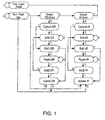
- the state diagram of the TAP controller is shown in Fig. 1.
- the test architecture includes an instruction register and a group of test data registers.
- the test data registers include at least a bypass register and a boundary-scan register.
- a block diagram of the test logic is illustrated in Fig. 2.
- IC integrated circuit
- MODE, SDO, SDI, and SCLK pins provide the in-system programming functions and the TMS, TDO, TDI, and TCK pins provide the boundary-scan testing functions. Because the pins of an integrated circuit package are considered a scarce resource, minimizing the number of pins is highly desirable. Therefore, it is desirable to reduce the number of pins required for in-system programming and boundary-scan testing.
- in-system programming and boundary-scan testing utilize different state machines to control each function. By eliminating one of these state machines, the silicon area required for such an IC would be reduced. Therefore, it is desirable to utilize the same state machine to control both in-system programming and boundary-scan testing.
- US Patent 4,602,210 addresses the problem of reducing the number of pins required for in-system programming and testing by sharing a set of pins using multiplexer and demultiplexer means.
- an in-system programmable logic decive as defined in claim I and a method for controlling an in-system programmable logic device as defined in claim 7 are provided, which device uses a common interface for accessing boundary scan testing and in-system programming functions.
- This common interface providing the shared use of a set of control pins, can be an interface invoking different state machines for boundary scan testing and in-system programming functions.
- the common state machine can be invoked according to a protocol of the control signals in a common physical interface.
- the common state machine executes an instruction set including different instructions for accomplishing boundary scan testing and in-system programming functions.
- An instruction register is used to select the function.
- test logic architecture similar to that specified in IEEE Standard 1149.1-1990, is utilized.
- the instruction register of the test architecture is modified to include private instructions which perform the desired programming functions.
- private instructions are similar to those discussed in Chapter 7.3 of the IEEE Standard.
- the present invention provides for both in-system programming and boundary-scan testing using only four dedicated pins.
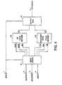
- Fig. 4 shows five pins of an integrated circuit package of the present invention. These pins include ISPEN (in-system programming enable) pin 1, SDI/TDI pin 2, SCLK/TCK pin 3, MODE/TMS pin 4, and SDO/TDO pin 5.
- the ISPEN pin 1 is coupled to input demultiplexer 12 and output multiplexer 14.
- the input demultiplexer 12 routes the signals on SCLK/TCK pin 2, MODE/TMS pin 3, and SDI/TDI pin 4, through to the ISP state machine 16 along the lines labeled SCLK, MODE and SDI, respectively.
- the high signal on ISPEN pin 1 causes the output multiplexer 14 to route the output (SDO) of the ISP state machine 16 through to SDO/TDO pin 5.
- the circuit When the signal on ISPEN pin 1 is low, the circuit may operate in either a boundary-scan test mode or a normal user mode. If the ISPEN pin 1 is low and there is a clock signal applied to SCLK/TCK pin 3, the integrated circuit operates in boundary-scan test mode. When the ISPEN pin 1 is low and there is no signal on SCLK/TCK pin 3, the integrated circuit operates in a normal user mode.
- the input demultiplexer 12 routes the signals on SCLK/TCK pin 2, MODE/TMS pin 3 and SDI/TDI pin 4 to the boundary-scan state machine 18 along the lines labeled TCK, TMS and TDI, respectively.
- the low signal on ISPEN pin 1 causes the output multiplexer 14 to route the output (TDO) of the boundary-scan state machine 18 through to SDO/TDO pin 5.
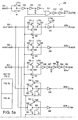
- FIG. 5 While the demultiplexing function may be performed in numerous ways, one demultiplexing circuit 500 is shown in Fig. 5.
- ISPEN pin 501, SCLK/TCK pin 502, MODE/TMS pin 503, and SDI/TDI pin 504 are external pins of an integrated circuit chip.
- SCLK node 502a, MODE node 503a, and SDI node 504a represent connections within the chip to ISP state machine 16.
- TCK node 502b, TMS node 503b, and TDI node 504b represent connections within the chip to boundary scan state machine 18.
- the boundary scan state machine 18 is enabled as follows.
- the signal on the ISPEN pin 501 is inverted by an inverter formed by transistors 506 and 507, and again inverted by inverter 508.
- the output of inverter 508 is provided directly to one terminal of NOR gate 511.
- the output of inverter 508 is also amplified by two inverters 509 and 510 before being provided to the other terminal of NOR gate 511.
- the output of NOR gate 511 is connected to inverters 512 and 513. Consequently, the inverse of the signal applied at ISPEN pin 501 appears at ISPEN node 501a. A high signal on ISPEN pin 501 therefore results in a low signal at ISPEN node 501a.
- a high signal on ISPEN pin 501 also causes transistors 521, 531 and 541 to remain off.
- the inverter formed by transistors 522-523, the inverter formed by transistors 532-533 and the inverter formed by transistors 542-543 are turned off.
- the signals present on SCLK node 502a, MODE node 503a and SDI node 504a are not responsive to the signals on SCLK/TCK pin 502, MODE/TMS pin 503 or SDI/TDI pin 504.
- the logic high signal on ISPEN pin 501 causes transistors 554, 564 and 574 to turn on. These transistors enable the inverter formed by transistors 551-552, the inverter formed by transistors 561-562, and the inverter formed by transistors 571-572, respectively.
- transistors 553, 563 and 573 are brought to a nonconductive state by the logic low signal on ISPEN node 501a. Consequently, the signals on SCLK/TCK pin 502, MODE/TMS pin 503 and SDI/TDI pin 504 are transmitted to TCK node 502b, TMS node 503b and TDI node 504b, respectively.
- the signal on SCLK/TCK pin 502 is first inverted by transistors 551-552, and then inverted by inverter 556 such that the original signal is provided to TCK node 502b.
- the ISP state machine 16 When the signal on ISPEN pin 501 is low, the ISP state machine 16 is enabled as follows. As previously described, the signal on the ISPEN pin 501 is inverted by elements 506-513, resulting in a logic high signal at ISPEN node 501a.
- transistors 521, 531 and 541 enable the inverter formed by transistors 522-523, the inverter formed by transistors 532-533, and the inverter formed by transistors 542-543, respectively.
- the signals on SCLK/TCK pin 502, MODE/TMS pin 503 and SDI/TDI pin 504 are inverted by transistors 522-523, transistors 532-533 or transistors 542-543, respectively.
- the signal originating on SCLK/TCK pin 502 is again inverted by inverter 526 such that the signal on SCLK/TCK pin 502 is transmitted to SCLK node 502a.
- the signal originating on MODE/TMS pin 503 is further inverted by inverter 536 such that the signal on MODE/TMS pin 503 is transmitted to MODE node 503a.
- the signal on SDI/TDI pin 504 is further inverted by inverters 546-550 such that the signal on SDI/TDI pin 504 is transmitted to SDI node 504a.
- transistors 554, 564 and 574 are turned off by the logic high signal on ISPEN node 501a. This disables the inverter formed by transistors 551-552, the inverter formed by transistors 561-562, and the inverter formed by transistors 571-572. In addition, transistors 553, 563 and 573 are brought to a conductive state, thereby supplying inverters 556, 566 and 576 with a ground voltage. Consequently, TCK node 502b, TMS node 503b, and TDI node 504b are all brought to a logic high state and are not responsive to any signals on SCLK/TCK pin 502, MODE/TMS pin 503 or SDI/TDI pin 504.
- ISP state machine 16 is disclosed in US patent application, Serial No. 07/695,356, filed 05/03/91 (now US-A-5 237 218).
- the boundary-scan state machine 18 While operating in the boundary-scan mode, the boundary-scan state machine 18 operates according to IEEE Standard 1149.1-1990. Using the above described configuration, the ISP state machine 16 and the boundary-scan state machine 18 may be implemented with five dedicated pins on the integrated circuit package.
- Fig. 6 illustrates a control circuit 600 of the embodiment of the present invention.
- a boundary-scan state machine is implemented in accordance with IEEE Standard 1149.1-1990.
- the state diagram of the tap controller state machine 610 is set forth in Fig. 1.
- the state of the tap controller state machine 610 is decoded by decoding logic block 611.
- the decoded state is used to control clock logic block 615, and control logic block 614.
- instruction register 612, instruction decode 613, bypass register 620, boundary-scan register 621, TCK pin 602, TMS pin 603, TDI pin 604 and TDO pin 605 are provided.
- the control circuit 600 of this embodiment is "instruction-based".
- instructions are received from TDI pin 604 and shifted in accordance with the state of TAP controller 610 into instruction register 612.
- the instruction in instruction register 612 is decoded by control logic 614, which controls the various data registers 620, 621, 622, 623, 624 and 625. Each of these data registers is used in one or more instructions of control circuit 600.
- the control logic block 614 loads bit-serial data on TDI pin 604 into the 1-bit bypass register 620. This bit-serial data is shifted out of bypass register 620 is then transmitted to the TDO pin 605 through the SDO multiplexer 616.
- boundary-scan register 621 When executing an instruction relating to a boundary-scan test operation, bit-serial data on TDI pin 604 can be shifted into N-bit boundary scan register 621.
- the operation of boundary-scan register 621 follows the requirements defined for boundary scan operations in IEEE Standard 1149.1-1990.
- the tap controller 610 is also used to perform the in-system programming function.
- the address shift register 622, the data shift register 623, the generic logic block (GLB) register 624 and the I/O register 625 are additionally provided. These registers are described in said US patent application Serial No. 07/695,356.
- Control logic block 614 controls these registers 622, 623, 624, 625 to perform in-system programming in accordance with the instruction in instruction register 612, as decoded by instruction decode logic 613. Because the tap controller state machine of this embodiment performs both the boundary-scan functions and the in-system programming, the ISPEN pin is not required. The multiplexing of pins 603-605 occurs within the circuit of Fig. 6 as the function of the circuit is switched from in-system programming to boundary-scan testing.
- Chapter 7.3 of IEEE Standard 1149.1-1990 allows for private instructions which may be defined by the component manufacturer.
- the present invention uses these private instructions to provide the instructions used for in-system programming.
- the private instructions may consist of any binary code other than those codes used for the defined public instruction codes, BYPASS, SAMPLE/PRELOAD and EXTEST.
- BYPASS code is defined as a logical "1" being entered into every instruction register cell.
- EXTEST code consists of a logical "0" being loaded into every instruction register cell.
- the SAMPLE/PRELOAD code is not defined by the standard, but may be defined by the component designer. Therefore, all codes other than all 1's or all 0's may be used as private instructions.
- PROGODD Program odd columns Program odd columns of array, pia and architecture cells at the rows selected by Address SR 010000 9.
- SFPRG Program security cell 010010 10.
- VERIFYEVEN Verify even columns programmed cells Verify even columns of array, pia and architecture programmed cells. Only one row can be selected for each verification 010100 11.
- VERIFYODD Verify odd columns programmed cells Verify odd columns of array, pia and architecture programmed cells. Only one row can be selected for each verification 010110 12.
- GLCPRELD Preload GLB registers 011000 13.
- IOPRELD Preload I/O Cell registers 011010 14.
- FLOWTHRU Flow through SDI flow through to SDO 011100 15.
- PROGESR Program ESR Address SR is automatically cleared to 0 011110 16.
- VERESR Verify ESR Address SR is automatically cleared to 0 100010 18.
- VEREVENH Verify even columns erased cells Verify even columns pia, array and architecture erased cells. Only one row can be selected for each verification 100100 19.
- VERODDH Verify odd columns erased cells Verify odd columns pia, array and architecture erased cells. Only one row can be selected for each verification 100110 20. NOP No operation 101000 31. INIT Initialize 111110
- the decoded instructions are provided from the instruction decode 613 to control logic 614.
- the control logic 614 directs the data received at TDI pin 604, according to the decoded instructions, into the selected one of address shift register 622, data shift register 623, GLB register 624 and input/output register 625. These four registers 622-625 perform the in-system programming of the chip.
- Clock logic block 615 provides the input clock signals for registers 612 and 620-625.
- the control logic block 614 and SDO multiplexer 616 operate to select which one of the registers 612, 620-625 will provide an output signal to TDO pin 605.
Description
- This invention relates to the design of integrated circuits, and in particular, to the design of programmable logic devices.
- Unlike a conventional programmable logic device (PLD), an in-system programmable logic device (ISPLD) can be reprogrammed in place, i.e. without removal from the system in which it is deployed. The method of reprogramming a programmable logic device in place is known as in-system programming (ISP). The standard pins utilized in in-system programming include a serial data input pin (SDI), a serial data output pin (SDO), a select mode pin (MODE) and a shift clock pin (SCLK). In-system programming is discussed in Application Serial No. 07/695,356, filed 05/03/91 and assigned to Lattice Semiconductor Corporation, which will issue as U.S. Patent 5,237,218 on August 17, 1993.
- U.S. Patent 5,237,218 allows an in-system programmable logic device to be implemented using only one dedicated in-system programming pin (ISP bar). The additional in-system programming pins (MODE, SCLK, SDI and SDO) are made available by multiplexing pins which are used as functional pins (such as input pins) when not in in-system programming mode. The in-system programming is controlled by an instruction-based state machine. An instruction set is provided to control the in-system programming activities.
- In integrated circuit testing, a technique called "boundary scan" has been developed in recent years. On February 15, 1990, the Institute of Electrical and Electronics Engineers (IEEE) approved standard 1149.1-1990. This standard defines a standard test logic architecture for implementing boundary scan functions which can be included in an integrated circuit for the purpose of testing the integrated circuit. The test architecture is defined to include a test access port (TAP) having connections for a test clock pin (TCK), a test mode select pin (TMS), a test data input pin (TDI) and a test data output pin (TDO). The test architecture also includes a TAP controller (boundary-scan state machine). The state diagram of the TAP controller is shown in Fig. 1. Finally, the test architecture includes an instruction register and a group of test data registers. The test data registers include at least a bypass register and a boundary-scan register. A block diagram of the test logic is illustrated in Fig. 2.
- FR-A-2 643 992 as well as P. Thorel et al. "Implementing boundary-scan and pseudo-random BIST in an asynchronous transfer mode switch.", IEEE International Test Conference 1991,
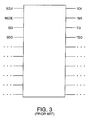
paper 5,2 & XP 000272243 disclose both boundary-scan applications according to the preamble ofclaim 1 and claim 7. - Previously, in order to provide bath in-system programming and standard test logic architecture in an integrated circuit (IC), eight pins were required. An example of a pin out of such an IC is illustrated in Fig. 3. The MODE, SDO, SDI, and SCLK pins provide the in-system programming functions and the TMS, TDO, TDI, and TCK pins provide the boundary-scan testing functions. Because the pins of an integrated circuit package are considered a scarce resource, minimizing the number of pins is highly desirable. Therefore, it is desirable to reduce the number of pins required for in-system programming and boundary-scan testing.
- In addition, in-system programming and boundary-scan testing utilize different state machines to control each function. By eliminating one of these state machines, the silicon area required for such an IC would be reduced. Therefore, it is desirable to utilize the same state machine to control both in-system programming and boundary-scan testing.
- US Patent 4,602,210 adresses the problem of reducing the number of pins required for in-system programming and testing by sharing a set of pins using multiplexer and demultiplexer means.
- In accordance with the present invention, an in-system programmable logic decive as defined in claim I and a method for controlling an in-system programmable logic device as defined in claim 7 are provided, which device uses a common interface for accessing boundary scan testing and in-system programming functions.
- This common interface, providing the shared use of a set of control pins, can be an interface invoking different state machines for boundary scan testing and in-system programming functions.
- The common state machine can be invoked according to a protocol of the control signals in a common physical interface. The common state machine executes an instruction set including different instructions for accomplishing boundary scan testing and in-system programming functions. An instruction register is used to select the function.
- While the in-system programming is enabled, selected pins will be used for in-system programming purposes. If the in-system programming is not enabled, the same selected pins will be used for boundary scan testing purposes.
- A test logic architecture, similar to that specified in IEEE Standard 1149.1-1990, is utilized. To implement the in-system programming instructions, the instruction register of the test architecture is modified to include private instructions which perform the desired programming functions. Such private instructions are similar to those discussed in Chapter 7.3 of the IEEE Standard.
- The present invention provides for both in-system programming and boundary-scan testing using only four dedicated pins.
- The present invention is better understood upon consideration of the following detailed description and the accompanying drawings.
-
- Fig. 1 shows the state diagram of a TAP controller under IEEE Standard 1149.1-1990;
- Fig. 2 shows a block diagram of the boundary-scan test logic according to IEEE Standard 1149.1-1990;
- Fig. 3 shows a pin-out diagram of a prior art in-system programmable logic device (ISPLD) having in-system programming pins, MODE, SCLK, SDI and SDO and boundary-scan testing pins TMS, TCK, TDI and TDO;
- Fig. 4 shows a block diagram according to embodiment which is not claimed having enable pin ISPEN and multiplexed in-system programming/boundary-scan test pins MODE/TMS, SCLK/TCK, SDI/TDI and SDO/TDO;
- Fig. 5 shows one embodiment of the demultiplexer block of Fig. 4; and
- Fig. 6 shows a block diagram according to the embodiment of the present invention.
-
- Fig. 4 shows five pins of an integrated circuit package of the present invention. These pins include ISPEN (in-system programming enable)
pin 1, SDI/TDI pin 2, SCLK/TCK pin 3, MODE/TMS pin 4, and SDO/TDO pin 5. TheISPEN pin 1 is coupled to inputdemultiplexer 12 and output multiplexer 14. When the signal onISPEN pin 1 is high, the circuit operates in the in-system programming mode. That is, theinput demultiplexer 12 routes the signals on SCLK/TCK pin 2, MODE/TMS pin 3, and SDI/TDI pin 4, through to theISP state machine 16 along the lines labeled SCLK, MODE and SDI, respectively. In addition, the high signal onISPEN pin 1 causes the output multiplexer 14 to route the output (SDO) of theISP state machine 16 through to SDO/TDO pin 5. - When the signal on
ISPEN pin 1 is low, the circuit may operate in either a boundary-scan test mode or a normal user mode. If theISPEN pin 1 is low and there is a clock signal applied to SCLK/TCK pin 3, the integrated circuit operates in boundary-scan test mode. When theISPEN pin 1 is low and there is no signal on SCLK/TCK pin 3, the integrated circuit operates in a normal user mode. - When the circuit is operating in a boundary-scan test mode, the
input demultiplexer 12 routes the signals on SCLK/TCK pin 2, MODE/TMS pin 3 and SDI/TDI pin 4 to the boundary-scan state machine 18 along the lines labeled TCK, TMS and TDI, respectively. In addition, the low signal onISPEN pin 1 causes the output multiplexer 14 to route the output (TDO) of the boundary-scan state machine 18 through to SDO/TDO pin 5. - While the demultiplexing function may be performed in numerous ways, one
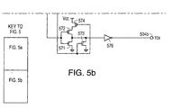
demultiplexing circuit 500 is shown in Fig. 5. In Fig. 5, ISPENpin 501, SCLK/TCK pin 502, MODE/TMS pin 503, and SDI/TDI pin 504 are external pins of an integrated circuit chip.SCLK node 502a,MODE node 503a, and SDI node 504a represent connections within the chip toISP state machine 16. TCK node 502b,TMS node 503b, andTDI node 504b, represent connections within the chip to boundaryscan state machine 18. - When the
ISPEN pin 501 is in a logic low state, the boundaryscan state machine 18 is enabled as follows. The signal on theISPEN pin 501 is inverted by an inverter formed bytransistors inverter 508. The output ofinverter 508 is provided directly to one terminal of NORgate 511. The output ofinverter 508 is also amplified by twoinverters gate 511. The output of NORgate 511 is connected toinverters ISPEN pin 501 appears atISPEN node 501a. A high signal onISPEN pin 501 therefore results in a low signal atISPEN node 501a. - When
ISPEN node 501a is in a logic low state, pull-uptransistors transistor 524 toinverter 526, resulting in a logic low state atSCLK node 502a. Similarly, the Vcc voltage is supplied throughtransistors inverter 536 and to inverters 546-550, respectively, resulting in logic low states atMODE node 503a and SDI node 504a. - A high signal on
ISPEN pin 501 also causestransistors - As a result, the signals present on
SCLK node 502a,MODE node 503a and SDI node 504a are not responsive to the signals on SCLK/TCK pin 502, MODE/TMS pin 503 or SDI/TDI pin 504. - In the lower portion of Fig. 5, the logic high signal on ISPEN pin 501 (logic low on
ISPEN node 501a) causestransistors transistors ISPEN node 501a. Consequently, the signals on SCLK/TCK pin 502, MODE/TMS pin 503 and SDI/TDI pin 504 are transmitted to TCK node 502b,TMS node 503b andTDI node 504b, respectively. For example, the signal on SCLK/TCK pin 502 is first inverted by transistors 551-552, and then inverted byinverter 556 such that the original signal is provided to TCK node 502b. - When the signal on
ISPEN pin 501 is low, theISP state machine 16 is enabled as follows. As previously described, the signal on theISPEN pin 501 is inverted by elements 506-513, resulting in a logic high signal atISPEN node 501a. - When the
ISPEN node 501a is at logic high, pull-uptransistors transistors transistors TCK pin 502, MODE/TMS pin 503 and SDI/TDI pin 504 are inverted by transistors 522-523, transistors 532-533 or transistors 542-543, respectively. The signal originating on SCLK/TCK pin 502 is again inverted byinverter 526 such that the signal on SCLK/TCK pin 502 is transmitted toSCLK node 502a. The signal originating on MODE/TMS pin 503 is further inverted byinverter 536 such that the signal on MODE/TMS pin 503 is transmitted toMODE node 503a. The signal on SDI/TDI pin 504 is further inverted by inverters 546-550 such that the signal on SDI/TDI pin 504 is transmitted to SDI node 504a. - In the lower portion of Fig. 5,
transistors ISPEN node 501a. This disables the inverter formed by transistors 551-552, the inverter formed by transistors 561-562, and the inverter formed by transistors 571-572. In addition,transistors inverters TMS node 503b, andTDI node 504b are all brought to a logic high state and are not responsive to any signals on SCLK/TCK pin 502, MODE/TMS pin 503 or SDI/TDI pin 504. - One embodiment of
ISP state machine 16 is disclosed in US patent application, Serial No. 07/695,356, filed 05/03/91 (now US-A-5 237 218). - While operating in the boundary-scan mode, the boundary-
scan state machine 18 operates according to IEEE Standard 1149.1-1990. Using the above described configuration, theISP state machine 16 and the boundary-scan state machine 18 may be implemented with five dedicated pins on the integrated circuit package. - Fig. 6 illustrates a
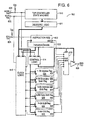
control circuit 600 of the embodiment of the present invention. In this embodiment, a boundary-scan state machine is implemented in accordance with IEEE Standard 1149.1-1990. Thus, the state diagram of the tapcontroller state machine 610 is set forth in Fig. 1. The state of the tapcontroller state machine 610 is decoded by decodinglogic block 611. The decoded state is used to controlclock logic block 615, and controllogic block 614. Also in accordance with IEEE Standard 1149.1-1990,instruction register 612,instruction decode 613,bypass register 620, boundary-scan register 621,TCK pin 602,TMS pin 603,TDI pin 604 andTDO pin 605 are provided. Thecontrol circuit 600 of this embodiment is "instruction-based". Thus, instructions are received fromTDI pin 604 and shifted in accordance with the state ofTAP controller 610 intoinstruction register 612. The instruction ininstruction register 612 is decoded bycontrol logic 614, which controls thevarious data registers control circuit 600. For example, when executing the bypass instruction, the control logic block 614 loads bit-serial data onTDI pin 604 into the 1-bit bypass register 620. This bit-serial data is shifted out ofbypass register 620 is then transmitted to theTDO pin 605 through theSDO multiplexer 616. When executing an instruction relating to a boundary-scan test operation, bit-serial data onTDI pin 604 can be shifted into N-bitboundary scan register 621. The operation of boundary-scan register 621 follows the requirements defined for boundary scan operations in IEEE Standard 1149.1-1990. - In this embodiment, the
tap controller 610 is also used to perform the in-system programming function. In order to perform in-system programming, theaddress shift register 622, thedata shift register 623, the generic logic block (GLB)register 624 and the I/O register 625 are additionally provided. These registers are described in said US patent application Serial No. 07/695,356.Control logic block 614 controls theseregisters instruction register 612, as decoded byinstruction decode logic 613. Because the tap controller state machine of this embodiment performs both the boundary-scan functions and the in-system programming, the ISPEN pin is not required. The multiplexing of pins 603-605 occurs within the circuit of Fig. 6 as the function of the circuit is switched from in-system programming to boundary-scan testing. - Chapter 7.3 of IEEE Standard 1149.1-1990 allows for private instructions which may be defined by the component manufacturer. The present invention uses these private instructions to provide the instructions used for in-system programming. The private instructions may consist of any binary code other than those codes used for the defined public instruction codes, BYPASS, SAMPLE/PRELOAD and EXTEST. The BYPASS code is defined as a logical "1" being entered into every instruction register cell. The EXTEST code consists of a logical "0" being loaded into every instruction register cell. The SAMPLE/PRELOAD code is not defined by the standard, but may be defined by the component designer. Therefore, all codes other than all 1's or all 0's may be used as private instructions. This flexibility allows the appropriate codes for in-system programming to be loaded into the instruction register. An example of a set of instructions for in-system programming is set forth in Table 1 below.
In System Programming Instructions CMD 0. NOP No operation 000001 1. ADDSHFT Address register shift 000010 2. DATASHFT Data register shift 000100 3. GBE Global bulk erase Erase pia, array, architecture and security cells 000110 4. PIABE PIA bulk erase Erase pia cells 001000 5. ARRBE Array bulk erase Erase array cells 001010 6. ARCHBE Architecture bulk erase Erase architecture cells 001100 7. PROGEVEN Program even columns Program even columns of array, pia and architecture cells at the rows selected by Address SR 001110 8. PROGODD Program odd columns Program odd columns of array, pia and architecture cells at the rows selected by Address SR 010000 9. SFPRG Program security cell 010010 10. VERIFYEVEN Verify even columns programmed cells Verify even columns of array, pia and architecture programmed cells. Only one row can be selected for each verification 010100 11. VERIFYODD Verify odd columns programmed cells Verify odd columns of array, pia and architecture programmed cells. Only one row can be selected for each verification 010110 12. GLCPRELD Preload GLB registers 011000 13. IOPRELD Preload I/O Cell registers 011010 14. FLOWTHRU Flow through SDI flow through to SDO 011100 15. PROGESR Program ESR Address SR is automatically cleared to 0 011110 16. ERAALL Erase all Erase pia, array, architecture, ES and security cells 100000 17. VERESR Verify ESR Address SR is automatically cleared to 0 100010 18. VEREVENH Verify even columns erased cells Verify even columns pia, array and architecture erased cells. Only one row can be selected for each verification 100100 19. VERODDH Verify odd columns erased cells Verify odd columns pia, array and architecture erased cells. Only one row can be selected for each verification 100110 20. NOP No operation 101000 31. INIT Initialize 111110 - The decoded instructions are provided from the
instruction decode 613 to controllogic 614. Thecontrol logic 614 directs the data received atTDI pin 604, according to the decoded instructions, into the selected one ofaddress shift register 622,data shift register 623, GLB register 624 and input/output register 625. These four registers 622-625 perform the in-system programming of the chip.Clock logic block 615 provides the input clock signals forregisters 612 and 620-625. Thecontrol logic block 614 andSDO multiplexer 616 operate to select which one of theregisters 612, 620-625 will provide an output signal toTDO pin 605. - The above detailed description is provided to illustrate the specific embodiment of the present invention described herein. It is appreciated that one skilled in the art will be able to provide numerous modifications and variations within the scope of the present invention upon consideration of the detailed description and the accompanying drawings. For example, although the IEEE 1149.1-1990 standard is used to illustrate the above embodiments of the present invention, the present invention is applicable to any other test architecture using a serial input pin, a serial output pin and a clock pin. The present invention is defined by the following claims.
Claims (11)
- An in-system programmable logic device comprising a common interface for accessing boundary scan testing and in-system programming functions, having a first state and a second state, said first state enabling in-system programming of said device and said second state enabling a boundary-scan test function of said device, said in-system programmable logic device further comprising:a first pin (603) for receiving a mode input signal (MODE) for performing in-system programming in said first state, said first pin (603) receiving a test mode select signal (TMS) for performing a boundary-scan test function in said second state;a second pin (604) for receiving a serial data input signal (SDI) for performing in-system programming in said first state, said second pin (604) receiving a test data input signal (TDI) for performing a boundary-scan test function in said second state;a third pin (602) for receiving a shift clock signal (SCLK) for performing in-system programming in said first state, said third pin (602) receiving a test clock signal (TCK) for performing a boundary-scan test function in said second state; anda fourth pin (605) for providing a serial data output (SDO) signal for performing in-system programming in said first state, said fourth pin (605) providing a test data output (TDO) signal for performing a boundary-scan function in said second state, further characterized in thatsaid first and second states are instruction-based, and in that said common interface comprises a common state machine (610) for performing both in-system programming of said device and boundary-scan testing said device, said state machine executing an instruction set including an instruction for an in-system programming function and an instruction for a boundary-scan testing function.
- The in-system programming logic device of claim 1, wherein said common interface distinguishes boundary-scan testing and in-system programming functions using a control signal protocol applied to a set of pins of said common interface.
- The in-system programmable logic device of claim 1, wherein said common interface invokes an in-system programming state machine (16) to perform in-system programming functions and a boundary-scan state machine (18) to perform boundary scan testing functions.
- The in-system programmable logic device of claim 3, wherein said state machine uses an instruction register (612), said instruction register (612) providing an instruction to perform said in-system programming of said device.
- The in-system programmable logic device of claim 4, wherein said state machine further comprises,
an address shift register (622);
a data shift register (623);
a GLB register (624); and
an input/output register (625);
wherein said address shift register (622), said data shift register (623), said GLB register (624) and said input/output register (625) receive said instructions from said instruction register (612). - The in-system programmable logic device of claim 3, 4 or 5, wherein said state machine meets the requirements of IEEE Standard 1149.1-1990.
- A method for controlling an in-system programmable logic device comprising the steps of:providing a common interface for accessing boundary scan testing and in-system programming functions; andinvoking through said common interface alternatively said boundary-scan testing functions and said in-system programming functions. according to instruction received via said common interface, wherein said step of invoking further comprises the steps of:invoking a first state and a second state of said device;accessing an in-system programming function of said device in said first state; andaccessing a boundary-scan test function of said device in said second state, said method further comprising the steps of:utilizing a signal on a first pin (603) as a mode input signal (MODE) for in-system programming in said first state and utilizing said signal on said first pin (603) as a test mode select signal (TMS) for boundary-scan testing in said second state;utilizing a signal on a second pin (604) as a serial data input signal (SDI) for in-system programming in said first state and utilizing said signal on said second pin (604) as a test data input signal (TDI) for boundary-scan testing in said second state;utilizing a signal on a third pin (602) as a shift clock signal (SCLK) for in-system programming in said first state and utilizing said signal on said third pin (602) as a test clock signal (TCK) for boundary-scan testing in said second state; andutilizing a signal on a fourth pin (605) as a serial data output signal (SDO) for in-system programming in said first state and utilizing said signal on said fourth pin (5) as a test data output signal (TDO) for boundary-scan testing in said second state, wherein the method is further characterized in that said first and second states are instruction-based and said step of providing a common interface comprises the step of providing a state machine (610) for performing both boundary-scan testing and in-system programming, said state machine executing instructions from an instruction set including an instruction for a boundary scan testing function and an instruction for an in-system programming function.
- The method of claim 7, wherein said step of providing a common interface comprises the steps of:providing an in-system programming state machine (16) to perform in-system programming functions; andproviding a boundary-scan testing state machine (18) to perform boundary-scan testing functions.
- The method of claim 7, wherein said step of providing a common interface provides an interface distinguishing boundary-scan testing and in-system programming functions according to a control signal protocol applied to a set of control pins of said interface.
- The method of claim 9, further comprising the step of loading an instruction register (612) in accordance with said state machine (610) to provide instructions to perform said in-system programming.
- The method of claim 9, wherein said state machine is a boundary-scan state machine in accordance with IEEE Standard 1149.1-1990.
Applications Claiming Priority (2)
| Application Number | Priority Date | Filing Date | Title |
|---|---|---|---|
| US08/106,263 US5412260A (en) | 1991-05-03 | 1993-08-13 | Multiplexed control pins for in-system programming and boundary scan state machines in a high density programmable logic device |
| US106263 | 2002-03-26 |
Publications (2)
| Publication Number | Publication Date |
|---|---|
| EP0639006A1 EP0639006A1 (en) | 1995-02-15 |
| EP0639006B1 true EP0639006B1 (en) | 2003-10-22 |
Family
ID=22310437
Family Applications (1)
| Application Number | Title | Priority Date | Filing Date |
|---|---|---|---|
| EP94202212A Expired - Lifetime EP0639006B1 (en) | 1993-08-13 | 1994-07-28 | Multiplexed control pins for in-system programming and boundary scan testing using state machines in a high density programmable logic device |
Country Status (4)
| Country | Link |
|---|---|
| US (1) | US5412260A (en) |
| EP (1) | EP0639006B1 (en) |
| JP (1) | JPH07175677A (en) |
| DE (2) | DE69433259D1 (en) |
Families Citing this family (68)
| Publication number | Priority date | Publication date | Assignee | Title |
|---|---|---|---|---|
| US5596734A (en) * | 1993-12-17 | 1997-01-21 | Intel Corporation | Method and apparatus for programming embedded memories of a variety of integrated circuits using the IEEE test access port |
| TW253031B (en) * | 1993-12-27 | 1995-08-01 | At & T Corp | |
| JPH0991957A (en) * | 1995-07-14 | 1997-04-04 | Mitsubishi Electric Corp | Mode selection circuit for semiconductor device |
| US5734868A (en) * | 1995-08-09 | 1998-03-31 | Curd; Derek R. | Efficient in-system programming structure and method for non-volatile programmable logic devices |
| US5706297A (en) * | 1995-08-24 | 1998-01-06 | Unisys Corporation | System for adapting maintenance operations to JTAG and non-JTAG modules |
| US5629635A (en) * | 1995-09-26 | 1997-05-13 | Ics Technologies, Inc. | Address programming via LED pin |
| US5717695A (en) * | 1995-12-04 | 1998-02-10 | Silicon Graphics, Inc. | Output pin for selectively outputting one of a plurality of signals internal to a semiconductor chip according to a programmable register for diagnostics |
| US5898701A (en) * | 1995-12-21 | 1999-04-27 | Cypress Semiconductor Corporation | Method and apparatus for testing a device |
| US5805794A (en) * | 1996-03-28 | 1998-09-08 | Cypress Semiconductor Corp. | CPLD serial programming with extra read register |
| US5835503A (en) * | 1996-03-28 | 1998-11-10 | Cypress Semiconductor Corp. | Method and apparatus for serially programming a programmable logic device |
| US5815510A (en) * | 1996-03-28 | 1998-09-29 | Cypress Semiconductor Corp. | Serial programming of instruction codes in different numbers of clock cycles |
| US5768288A (en) * | 1996-03-28 | 1998-06-16 | Cypress Semiconductor Corp. | Method and apparatus for programming a programmable logic device having verify logic for comparing verify data read from a memory location with program data |
| US5869979A (en) | 1996-04-05 | 1999-02-09 | Altera Corporation | Technique for preconditioning I/Os during reconfiguration |
| US5870410A (en) * | 1996-04-29 | 1999-02-09 | Altera Corporation | Diagnostic interface system for programmable logic system development |
| US5864486A (en) * | 1996-05-08 | 1999-01-26 | Lattice Semiconductor Corporation | Method and apparatus for in-system programming of a programmable logic device using a two-wire interface |
| US5764076A (en) * | 1996-06-26 | 1998-06-09 | Xilinx, Inc. | Circuit for partially reprogramming an operational programmable logic device |
| GB2346473B (en) * | 1996-07-18 | 2000-12-27 | Altera Corp | Configuration memory |
| US6097211A (en) * | 1996-07-18 | 2000-08-01 | Altera Corporation | Configuration memory integrated circuit |
| US6804725B1 (en) * | 1996-08-30 | 2004-10-12 | Texas Instruments Incorporated | IC with state machine controlled linking module |
| US5805607A (en) * | 1996-10-22 | 1998-09-08 | Advanced Micro Devices, Inc. | Method for user-controlled I/O switching during in-circuit programming of CPLDs through the IEEE 1149.1 test access port |
| US5867037A (en) * | 1996-10-24 | 1999-02-02 | International Business Machines Corporation | Method and apparatus of programming FPGA devices through ASIC devices |
| US5825199A (en) * | 1997-01-30 | 1998-10-20 | Vlsi Technology, Inc. | Reprogrammable state machine and method therefor |
| EP0862063A1 (en) * | 1997-02-27 | 1998-09-02 | Siemens Aktiengesellschaft | Control of a test interface |
| GB9707364D0 (en) * | 1997-04-11 | 1997-05-28 | Eidos Technologies Limited | A method and a system for processing digital information |
| US6421812B1 (en) * | 1997-06-10 | 2002-07-16 | Altera Corporation | Programming mode selection with JTAG circuits |
| US6691267B1 (en) | 1997-06-10 | 2004-02-10 | Altera Corporation | Technique to test an integrated circuit using fewer pins |
| US6034857A (en) * | 1997-07-16 | 2000-03-07 | Altera Corporation | Input/output buffer with overcurrent protection circuit |
| US6011744A (en) * | 1997-07-16 | 2000-01-04 | Altera Corporation | Programmable logic device with multi-port memory |
| US6020760A (en) * | 1997-07-16 | 2000-02-01 | Altera Corporation | I/O buffer circuit with pin multiplexing |
| US6108807A (en) * | 1997-07-28 | 2000-08-22 | Lucent Technologies Inc. | Apparatus and method for hybrid pin control of boundary scan applications |
| US6032279A (en) * | 1997-11-07 | 2000-02-29 | Atmel Corporation | Boundary scan system with address dependent instructions |
| US5848026A (en) * | 1997-12-08 | 1998-12-08 | Atmel Corporation | Integrated circuit with flag register for block selection of nonvolatile cells for bulk operations |
| US5968196A (en) * | 1998-04-21 | 1999-10-19 | Atmel Corporation | Configuration control in a programmable logic device using non-volatile elements |
| US6304099B1 (en) * | 1998-05-21 | 2001-10-16 | Lattice Semiconductor Corporation | Method and structure for dynamic in-system programming |
| US6430719B1 (en) * | 1998-06-12 | 2002-08-06 | Stmicroelectronics, Inc. | General port capable of implementing the JTAG protocol |
| JP2000065899A (en) | 1998-08-14 | 2000-03-03 | Sony Corp | Semiconductor device, and its data rewriting method |
| US6742150B1 (en) | 1998-09-29 | 2004-05-25 | Siemens Aktiengesellschaft | Low redesign application-specific module |
| US6158034A (en) * | 1998-12-03 | 2000-12-05 | Atmel Corporation | Boundary scan method for terminating or modifying integrated circuit operating modes |
| US7013415B1 (en) * | 1999-05-26 | 2006-03-14 | Renesas Technology Corp. | IC with internal interface switch for testability |
| US6618839B1 (en) | 1999-11-30 | 2003-09-09 | Synplicity, Inc. | Method and system for providing an electronic system design with enhanced debugging capabilities |
| US7065481B2 (en) | 1999-11-30 | 2006-06-20 | Synplicity, Inc. | Method and system for debugging an electronic system using instrumentation circuitry and a logic analyzer |
| US7356786B2 (en) * | 1999-11-30 | 2008-04-08 | Synplicity, Inc. | Method and user interface for debugging an electronic system |
| US6931572B1 (en) | 1999-11-30 | 2005-08-16 | Synplicity, Inc. | Design instrumentation circuitry |
| US6823497B2 (en) | 1999-11-30 | 2004-11-23 | Synplicity, Inc. | Method and user interface for debugging an electronic system |
| US7072818B1 (en) * | 1999-11-30 | 2006-07-04 | Synplicity, Inc. | Method and system for debugging an electronic system |
| US6803785B1 (en) | 2000-06-12 | 2004-10-12 | Altera Corporation | I/O circuitry shared between processor and programmable logic portions of an integrated circuit |
| US7340596B1 (en) | 2000-06-12 | 2008-03-04 | Altera Corporation | Embedded processor with watchdog timer for programmable logic |
| US6961884B1 (en) | 2000-06-12 | 2005-11-01 | Altera Corporation | JTAG mirroring circuitry and methods |
| US7222315B2 (en) * | 2000-11-28 | 2007-05-22 | Synplicity, Inc. | Hardware-based HDL code coverage and design analysis |
| GB2379524A (en) * | 2001-09-06 | 2003-03-12 | Nec Technologies | Multiplexing pins on an ASIC |
| US6898750B2 (en) | 2002-01-16 | 2005-05-24 | Microtune (San Diego), Inc. | In-chip monitoring system to monitor input/output of functional blocks |
| US7249298B2 (en) | 2002-04-30 | 2007-07-24 | Samsung Electronics Co., Ltd. | Multiple scan chains with pin sharing |
| US7424658B1 (en) | 2002-07-01 | 2008-09-09 | Altera Corporation | Method and apparatus for testing integrated circuits |
| TW569221B (en) * | 2002-09-11 | 2004-01-01 | Elan Microelectronics Corp | Chip having on-system programmable nonvolatile memory and off-system programmable nonvolatile memory, and forming method and programming method of the same |
| US7010733B2 (en) * | 2002-10-09 | 2006-03-07 | International Business Machines Corporation | Parametric testing for high pin count ASIC |
| US7191265B1 (en) | 2003-04-29 | 2007-03-13 | Cisco Technology, Inc. | JTAG and boundary scan automatic chain selection |
| CN100351638C (en) * | 2003-05-01 | 2007-11-28 | 中兴通讯股份有限公司 | Boundary scan testing device for integrated circuit |
| CN100348992C (en) * | 2003-11-19 | 2007-11-14 | 华为技术有限公司 | Testing method of peripheral interconnecting wire |
| US7332928B2 (en) * | 2004-03-05 | 2008-02-19 | Finisar Corporation | Use of a third state applied to a digital input terminal of a circuit to initiate non-standard operational modes of the circuit |
| US8205186B1 (en) | 2005-04-11 | 2012-06-19 | Synopsys, Inc. | Incremental modification of instrumentation logic |
| US7518397B2 (en) * | 2007-01-03 | 2009-04-14 | International Rectifier Corporation | Chip with in-circuit programability |
| TWI343773B (en) * | 2007-10-19 | 2011-06-11 | Realtek Semiconductor Corp | Microelectronic device and pin arrangement method thereof |
| WO2009063359A1 (en) * | 2007-11-14 | 2009-05-22 | Koninklijke Philips Electronics N.V. | General purpose serial communication using jtag interface |
| JP5167904B2 (en) * | 2008-03-28 | 2013-03-21 | 富士通株式会社 | Scan control method, scan control circuit and apparatus |
| US10162000B2 (en) * | 2012-02-16 | 2018-12-25 | Nxp B.V. | Testing an integrated circuit device with multiple testing protocols |
| US9742847B2 (en) * | 2013-08-30 | 2017-08-22 | Texas Instruments Incorporated | Network node physical/communication pins, state machines, interpreter and executor circuitry |
| US9817066B1 (en) * | 2014-08-26 | 2017-11-14 | Xilinx, Inc. | Configurable JTAG-to-serial bus translator |
| CN111665432B (en) * | 2020-05-22 | 2022-10-25 | 中国人民解放军国防科技大学 | Verification method, device, equipment and storage medium for chip pin multiplexing module |
Citations (1)
| Publication number | Priority date | Publication date | Assignee | Title |
|---|---|---|---|---|
| FR2643992A1 (en) * | 1989-03-06 | 1990-09-07 | Nec Corp | Data processing system, capable of storing control data in a control memory with enhanced speed |
Family Cites Families (22)
| Publication number | Priority date | Publication date | Assignee | Title |
|---|---|---|---|---|
| US4870302A (en) * | 1984-03-12 | 1989-09-26 | Xilinx, Inc. | Configurable electrical circuit having configurable logic elements and configurable interconnects |
| US4855954A (en) * | 1985-03-04 | 1989-08-08 | Lattice Semiconductor Corporation | In-system programmable logic device with four dedicated terminals |
| US4833646A (en) * | 1985-03-04 | 1989-05-23 | Lattice Semiconductor Corp. | Programmable logic device with limited sense currents and noise reduction |
| US4887239A (en) * | 1985-03-04 | 1989-12-12 | Lattice Semiconductor Corporation | One-time programmable data security system for programmable logic device |
| US4766569A (en) * | 1985-03-04 | 1988-08-23 | Lattice Semiconductor Corporation | Programmable logic array |
| US4896296A (en) * | 1985-03-04 | 1990-01-23 | Lattice Semiconductor Corporation | Programmable logic device configurable input/output cell |
| US4761768A (en) * | 1985-03-04 | 1988-08-02 | Lattice Semiconductor Corporation | Programmable logic device |
| US4852044A (en) * | 1985-03-04 | 1989-07-25 | Lattice Semiconductor Corporation | Programmable data security circuit for programmable logic device |
| US4879688A (en) * | 1985-03-04 | 1989-11-07 | Lattice Semiconductor Corporation | In-system programmable logic device |
| US4857774A (en) * | 1986-09-19 | 1989-08-15 | Actel Corporation | Testing apparatus and diagnostic method for use with programmable interconnect architecture |
| US4918641A (en) * | 1987-08-26 | 1990-04-17 | Ict International Cmos Technology, Inc. | High-performance programmable logic device |
| JPS6478023A (en) * | 1987-09-18 | 1989-03-23 | Fujitsu Ltd | Programmable logic device |
| JP2541248B2 (en) * | 1987-11-20 | 1996-10-09 | 三菱電機株式会社 | Programmable logic array |
| US5023606A (en) * | 1988-01-13 | 1991-06-11 | Plus Logic, Inc. | Programmable logic device with ganged output pins |
| KR910005615B1 (en) * | 1988-07-18 | 1991-07-31 | 삼성전자 주식회사 | Programmable sequential code recognition circuit |
| US5023484A (en) * | 1988-09-02 | 1991-06-11 | Cypress Semiconductor Corporation | Architecture of high speed synchronous state machine |
| JP2650124B2 (en) * | 1989-07-11 | 1997-09-03 | 三菱電機株式会社 | Semiconductor integrated circuit |
| JPH0756749B2 (en) * | 1989-09-29 | 1995-06-14 | 株式会社東芝 | Function selection circuit |
| US5027011A (en) * | 1989-10-31 | 1991-06-25 | Sgs-Thomson Microelectronics, Inc. | Input row drivers for programmable logic devices |
| US5072138A (en) * | 1990-08-17 | 1991-12-10 | Sgs-Thomson Microelectronics, Inc. | Semiconductor memory with sequential clocked access codes for test mode entry |
| IT1246301B (en) * | 1990-10-22 | 1994-11-17 | St Microelectronics Srl | SCAN PATH OPERATIONAL ANALYSIS DEVICE WITH SINGLE SCAN CLOCK AND SINGLE OUTPUT PHASE FOR INTEGRATED CIRCUIT. |
| US5237218A (en) * | 1991-05-03 | 1993-08-17 | Lattice Semiconductor Corporation | Structure and method for multiplexing pins for in-system programming |
-
1993
- 1993-08-13 US US08/106,263 patent/US5412260A/en not_active Expired - Lifetime
-
1994
- 1994-07-28 DE DE69433259T patent/DE69433259D1/en not_active Expired - Lifetime
- 1994-07-28 DE DE0639006T patent/DE639006T1/en active Pending
- 1994-07-28 EP EP94202212A patent/EP0639006B1/en not_active Expired - Lifetime
- 1994-08-12 JP JP21192294A patent/JPH07175677A/en active Pending
Patent Citations (1)
| Publication number | Priority date | Publication date | Assignee | Title |
|---|---|---|---|---|
| FR2643992A1 (en) * | 1989-03-06 | 1990-09-07 | Nec Corp | Data processing system, capable of storing control data in a control memory with enhanced speed |
Non-Patent Citations (2)
| Title |
|---|
| 1990 IEEE Standard 1149.1-1990 * |
| THOREL P., ET AL.: "IMPLEMENTING BOUNDARY-SCAN AND PSEUDO-RANDOM BIST IN AN ASYNCHRONOUS TRANSFER MODE SWITCH.", PROCEEDINGS OF THE INTERNATIONAL TEST CONFERENCE. NASHVILLE, OCT. 28 - 30, 1991., NEW YORK, IEEE., US, 15 May 1992 (1992-05-15), US, pages 131 - 139., XP000272243, ISBN: 978-0-8186-9156-0 * |
Also Published As
| Publication number | Publication date |
|---|---|
| DE69433259D1 (en) | 2003-11-27 |
| US5412260A (en) | 1995-05-02 |
| JPH07175677A (en) | 1995-07-14 |
| EP0639006A1 (en) | 1995-02-15 |
| DE639006T1 (en) | 1996-02-15 |
Similar Documents
| Publication | Publication Date | Title |
|---|---|---|
| EP0639006B1 (en) | Multiplexed control pins for in-system programming and boundary scan testing using state machines in a high density programmable logic device | |
| EP0602973B1 (en) | Mixed signal integrated circuit architecture and test methodology | |
| US5237218A (en) | Structure and method for multiplexing pins for in-system programming | |
| US6191603B1 (en) | Modular embedded test system for use in integrated circuits | |
| US5867507A (en) | Testable programmable gate array and associated LSSD/deterministic test methodology | |
| US6711707B2 (en) | Process of controlling plural test access ports | |
| US8713389B2 (en) | Tap and linking module TDO register, gating for TCK and TMS | |
| EP0868667B1 (en) | High impedance test mode for jtag | |
| KR101118407B1 (en) | Test architecture and method | |
| US6026039A (en) | Parallel test circuit for semiconductor memory | |
| JP2000275303A (en) | Method and device for boundary scan test | |
| US6289477B1 (en) | Fast-scan-flop and integrated circuit device incorporating the same | |
| JP2000009799A (en) | Semiconductor device | |
| EP0158006A2 (en) | Electronically selectable redundant array (ESRA) | |
| US7954017B2 (en) | Multiple embedded memories and testing components for the same | |
| WO1999066338A1 (en) | Using power-on mode to control test mode | |
| US20020199143A1 (en) | Method and apparatus for testing circuit modules | |
| KR20050032613A (en) | Integrated circuit with embedded identification code |
Legal Events
| Date | Code | Title | Description |
|---|---|---|---|
| PUAI | Public reference made under article 153(3) epc to a published international application that has entered the european phase |
Free format text: ORIGINAL CODE: 0009012 |
|
| AK | Designated contracting states |
Kind code of ref document: A1 Designated state(s): DE GB IT |
|
| 17P | Request for examination filed |
Effective date: 19950425 |
|
| ITCL | It: translation for ep claims filed |
Representative=s name: NOTARBARTOLO & GERVASI S.R.L. |
|
| DET | De: translation of patent claims | ||
| 17Q | First examination report despatched |
Effective date: 19961106 |
|
| APAB | Appeal dossier modified |
Free format text: ORIGINAL CODE: EPIDOS NOAPE |
|
| APAB | Appeal dossier modified |
Free format text: ORIGINAL CODE: EPIDOS NOAPE |
|
| APAD | Appeal reference recorded |
Free format text: ORIGINAL CODE: EPIDOS REFNE |
|
| APAB | Appeal dossier modified |
Free format text: ORIGINAL CODE: EPIDOS NOAPE |
|
| GRAG | Despatch of communication of intention to grant |
Free format text: ORIGINAL CODE: EPIDOS AGRA |
|
| GRAG | Despatch of communication of intention to grant |
Free format text: ORIGINAL CODE: EPIDOS AGRA |
|
| GRAH | Despatch of communication of intention to grant a patent |
Free format text: ORIGINAL CODE: EPIDOS IGRA |
|
| GRAH | Despatch of communication of intention to grant a patent |
Free format text: ORIGINAL CODE: EPIDOS IGRA |
|
| GRAA | (expected) grant |
Free format text: ORIGINAL CODE: 0009210 |
|
| AK | Designated contracting states |
Kind code of ref document: B1 Designated state(s): DE GB IT |
|
| PG25 | Lapsed in a contracting state [announced via postgrant information from national office to epo] |
Ref country code: IT Free format text: LAPSE BECAUSE OF FAILURE TO SUBMIT A TRANSLATION OF THE DESCRIPTION OR TO PAY THE FEE WITHIN THE PRE;WARNING: LAPSES OF ITALIAN PATENTS WITH EFFECTIVE DATE BEFORE 2007 MAY HAVE OCCURRED AT ANY TIME BEFORE 2007. THE CORRECT EFFECTIVE DATE MAY BE DIFFERENT FROM THE ONE RECORDED.SCRIBED TIME-LIMIT Effective date: 20031022 |
|
| REG | Reference to a national code |
Ref country code: GB Ref legal event code: FG4D |
|
| REF | Corresponds to: |
Ref document number: 69433259 Country of ref document: DE Date of ref document: 20031127 Kind code of ref document: P |
|
| PG25 | Lapsed in a contracting state [announced via postgrant information from national office to epo] |
Ref country code: DE Free format text: LAPSE BECAUSE OF FAILURE TO SUBMIT A TRANSLATION OF THE DESCRIPTION OR TO PAY THE FEE WITHIN THE PRESCRIBED TIME-LIMIT Effective date: 20040123 |
|
| PLBE | No opposition filed within time limit |
Free format text: ORIGINAL CODE: 0009261 |
|
| STAA | Information on the status of an ep patent application or granted ep patent |
Free format text: STATUS: NO OPPOSITION FILED WITHIN TIME LIMIT |
|
| 26N | No opposition filed |
Effective date: 20040723 |
|
| APAH | Appeal reference modified |
Free format text: ORIGINAL CODE: EPIDOSCREFNO |
|
| PGFP | Annual fee paid to national office [announced via postgrant information from national office to epo] |
Ref country code: GB Payment date: 20130724 Year of fee payment: 20 |
|
| REG | Reference to a national code |
Ref country code: GB Ref legal event code: PE20 Expiry date: 20140727 |
|
| PG25 | Lapsed in a contracting state [announced via postgrant information from national office to epo] |
Ref country code: GB Free format text: LAPSE BECAUSE OF EXPIRATION OF PROTECTION Effective date: 20140727 |