EP0640488B1 - Improvements in or relating to printing - Google Patents
Improvements in or relating to printing Download PDFInfo
- Publication number
- EP0640488B1 EP0640488B1 EP94113311A EP94113311A EP0640488B1 EP 0640488 B1 EP0640488 B1 EP 0640488B1 EP 94113311 A EP94113311 A EP 94113311A EP 94113311 A EP94113311 A EP 94113311A EP 0640488 B1 EP0640488 B1 EP 0640488B1
- Authority
- EP
- European Patent Office
- Prior art keywords
- light
- pixel
- data
- phases
- elements
- Prior art date
- Legal status (The legal status is an assumption and is not a legal conclusion. Google has not performed a legal analysis and makes no representation as to the accuracy of the status listed.)
- Expired - Lifetime
Links
Images


Classifications
-
- G—PHYSICS
- G06—COMPUTING; CALCULATING OR COUNTING
- G06K—GRAPHICAL DATA READING; PRESENTATION OF DATA; RECORD CARRIERS; HANDLING RECORD CARRIERS
- G06K15/00—Arrangements for producing a permanent visual presentation of the output data, e.g. computer output printers
- G06K15/02—Arrangements for producing a permanent visual presentation of the output data, e.g. computer output printers using printers
- G06K15/12—Arrangements for producing a permanent visual presentation of the output data, e.g. computer output printers using printers by photographic printing, e.g. by laser printers
-
- H—ELECTRICITY
- H04—ELECTRIC COMMUNICATION TECHNIQUE
- H04N—PICTORIAL COMMUNICATION, e.g. TELEVISION
- H04N1/00—Scanning, transmission or reproduction of documents or the like, e.g. facsimile transmission; Details thereof
- H04N1/40—Picture signal circuits
- H04N1/40025—Circuits exciting or modulating particular heads for reproducing continuous tone value scales
- H04N1/40043—Circuits exciting or modulating particular heads for reproducing continuous tone value scales using more than one type of modulation, e.g. pulse width modulation and amplitude modulation
-
- G—PHYSICS
- G06—COMPUTING; CALCULATING OR COUNTING
- G06K—GRAPHICAL DATA READING; PRESENTATION OF DATA; RECORD CARRIERS; HANDLING RECORD CARRIERS
- G06K15/00—Arrangements for producing a permanent visual presentation of the output data, e.g. computer output printers
- G06K15/02—Arrangements for producing a permanent visual presentation of the output data, e.g. computer output printers using printers
- G06K15/12—Arrangements for producing a permanent visual presentation of the output data, e.g. computer output printers using printers by photographic printing, e.g. by laser printers
- G06K15/1238—Arrangements for producing a permanent visual presentation of the output data, e.g. computer output printers using printers by photographic printing, e.g. by laser printers simultaneously exposing more than one point
-
- H—ELECTRICITY
- H04—ELECTRIC COMMUNICATION TECHNIQUE
- H04N—PICTORIAL COMMUNICATION, e.g. TELEVISION
- H04N1/00—Scanning, transmission or reproduction of documents or the like, e.g. facsimile transmission; Details thereof
- H04N1/40—Picture signal circuits
- H04N1/40025—Circuits exciting or modulating particular heads for reproducing continuous tone value scales
- H04N1/40031—Circuits exciting or modulating particular heads for reproducing continuous tone value scales for a plurality of reproducing elements simultaneously
-
- H—ELECTRICITY
- H04—ELECTRIC COMMUNICATION TECHNIQUE
- H04N—PICTORIAL COMMUNICATION, e.g. TELEVISION
- H04N1/00—Scanning, transmission or reproduction of documents or the like, e.g. facsimile transmission; Details thereof
- H04N1/40—Picture signal circuits
- H04N1/40062—Discrimination between different image types, e.g. two-tone, continuous tone
Definitions
- This invention relates generally to the field of printing, and more particularly to a method and apparatus for printing stroke and contone data together.
- Hard copy devices such as printers, generally print two kinds of data.
- the first type of data is stroke data, usually text and graphics data.
- the second type of data is continuous tone ("contone”) data, which is usually image data, for example, a data representation of a photographic image.
- High quality rendering of stroke data requires a printer that can produce a spatial resolution of 600 dots per inch (“dpi”) or more. This resolution is required, for example, to reduce jaggedness of diagonal edges or to reproduce fine seriphs in text.
- Contone data does not require such high spatial resolution, but requires a printer than can produce gray shades. Indeed, if the printer is capable of producing 256 gray shades (which is typical intensity resolution of image scanners), a 200-250 dpi printer will generally suffice. Such a printer provides appropriate spatial resolution for the human eye to perceive smooth shades.
- printers are binary printers that can reproduce only two gray shades, black and white. These printers simulate more gray shades by logically combining several dots into cells and relying on the spatial integration property of the human eye to stimulate smooth shades.
- a 3200 dpi printer can achieve appropriate gray shades by forming cells from 16 X 16 arrays of dots, resulting in 200 cells per inch (sometimes referred to as lines per inch). By controlling the number of dots that are black (or white) in this array, each cell can represent up to 257 gray levels (0 through 256, with 256 represented by all dots being black). The spatial resolution of the human eye will perceive smooth shades with such a printer.
- EP-A-0 540 221 sets forth a printer using a laser scanning apparatus and discloses the idea of using "small pixels" within an "objective pixel” to achieve halftone printing. However, the pixels are not formed using a spatial light modulator array of elements.
- EP-A-0 361 880 which discloses an image signal processor, distinguishes between character data and halftone image data and applies an error diffusion process and binarisation process to the halftone image data and character data, respectively. This document is also directed to half-toning.
- the image signal processor comprises an image signal identification means for outputting a kind-identification signal of said input image signal based on a detected power at a fixed frequency at least in a direction of the main scanning or subscanning of the input image signal.
- EP-A-0 556 591 discloses a printer using an array of deformable mirror devices (DMD), a photoconductive drum and a processor for controlling the spatial light modulator such that predetermined areas of the photoconductive drum render gray scale levels.
- DMD deformable mirror devices
- EP-A-0 620 676 discloses a process and architecture for a digital micromirror printer for achieving high resolution, high-speed gray scale printing with binary spatial light modulators.
- the process comprises illuminating a SLM having a plurality of rows of elements; using the SLM elements to modulate light in conjunction with movement of a photoconductive surface having a process direction, and converting grayscale information into codes that coordinate reflecting light from selected individual elements of the plurality of rows of said SLM with motion of the photoconductive surface, to reflect light on predetermined areas of the photoconductive surface that corresponds to that grayscale information. Additionaly, each pixel can be divided up into four phases in the process direction and printed in phase pairs.
- a method and apparatus for printing stroke and contone data together is provided which substantially eliminates or reduces disadvantages and problems associated with prior art printers and printing techniques.
- a method of printing both stroke and contone data together in which data to be printed is identified as either contone data or stroke data.
- the contone data is then rendered with intensity modulation and spatial modulation in the process and cross-process directions, and the stroke data is rendered with intensity modulation.
- contone data is rendered by reflecting the light from predetermined individual elements of a plurality of rows onto predetermined phases of pixels of a photoconductive drum, the predetermined phases rendering the pixels at image quality gray scale levels.
- Stroke data is rendered by reflecting the light from predetermined individual elements onto predetermined phases of the photoconductive drum, the predetermined phases rendering the stroke data at high resolution.
- An important technical advantage of the present invention is that the different requirements of stroke and contone data are satisfied by using different methods to render them by exploiting spatial and intensity modulation capabilities of a DMD based printer.
- FIGURE 1 illustrates a printer 10 constructed according to the teachings of the present invention.
- a spatial light modulator SLM having individual elements making up an array 12 is provided.
- array 12 comprises an array of DMDs.
- individual elements of the array 12 will be referred to as mirrors.
- Array 12 may comprise an array of DMDs constructed as disclosed in U.S. Patent No. 4,956,619, "Spatial Light Modulator.”
- each row of array 12 is staggered, such that individual mirrors (elements) are offset from row to row. This offset will be exploited, as discussed below, to allow for generation of many gray scales for the printing of image data and for the printing of smooth edges for graphics data. Only a portion of array 12 is shown for clarity, it being understood that array 12 may include more rows or columns, as particular applications require.
- Light from a light source 14 is reflected by array 12 either onto or off of OPC drum 16.
- Light source 14 may comprise a light-emitting diode.
- Light from array 12 may be reflected directly onto OPC drum 16 or focused through optics 18.
- OPC drum 16 Only a line of logical pixels is shown for clarity, it being understood that several lines of pixels can be simultaneously illuminated by the DMD array. Each of these pixels will be illuminated and thereby either charged or discharged for toner attraction. The drum 16 will then rotate over the page to be printed, and the toner will be transferred from the drum 16 to the page, the line of pixels printing a line on the page.
- an exemplary pixel 20 receives light from mirrors 22-36 of array 12. The light is received from each row of mirrors at different time instances as the drum rotates. Likewise, mirrors 38-52 reflect light onto pixel 54 of OPC drum 16. Pixel 21 is also shown, and will be discussed below. Pixel 21 will be exposed by mirrors 22-36 as OPC drum 16 rotates.
- FIGUREs 2a-2h illustrate light received at pixel 20 from each of the mirrors 22-36.
- light from mirrors 22 and 24 first impinges on the top of pixel 20.
- the mirrors of array 12 shine light on an area approximately 1 ⁇ 4 the area of pixel 20.
- pixel 20 may be 1/300 of an inch by 1/300 of an inch, whereas the light from mirror 22 may be 1/600 of an inch by 1/600 of an inch. It should be understood that other sized and shaped pixels and mirrors are possible, or the effective size of the mirrors may be altered through optics 18.
- phase 20 The particular area on pixel 20 on which light from any one mirror falls is referred to as a phase.
- a phase The particular area on pixel 20 on which light from any one mirror falls is referred to as a phase.
- FIGURE 2a light from mirrors 22 and 24 fall on phases A and B, shown by the circled A and B.
- the duration for which the light falls can be controlled by switching the mirrors OFF or alternatively switching the light source OFF.
- FIGURE 2b as time goes on and the OPC drum 16 rotates, in this example by a quarter of a pixel, light from mirrors 22 and 24 falls on phases C and D.
- phase H falls half on pixel 20 and half on the adjacent pixel of OPC drum 16.
- This light falling on the adjacent pixel can be handled in one of two ways. First, it can be taken into account in determining the gray scale to be generated in the adjacent pixel. Thus, if the gray scale of the adjacent pixel is to be, for example, level 200 of 256 gray levels, the amount of light received on that pixel from phase H can be taken into account. Alternatively, the light received from phase H on the adjacent pixel can be disregarded. Indeed, if the adjacent pixel is to be completely white, then this is the only alternative, and there will be some blur between pixels.
- phase I and J As shown in FIGURE 2d, as OPC drum 16 continues to rotate, the light from mirrors 22 and 24 falls on phases I and J. As discussed above in connection with FIGURE 2c, phases I and J overlap on to the pixel of the next line of OPC drum 16. This overlap can either be taken into account in determining the gray scale to be generated on that pixel, or disregarded. The light from mirrors 26 and 28 falls on phases K and L.
- Intensity modulation is achieved at each phase by choosing to turn the mirror ON or OFF (the ON position corresponds to the case where the light is reflected on the OPC pixel and the OFF position corresponds to the case where the light is reflected away from the OPC).
- the ON position corresponds to the case where the light is reflected on the OPC pixel and the OFF position corresponds to the case where the light is reflected away from the OPC.
- three levels of exposure may be generated for each phase by exposing each phase zero, one, or two times. For example, to generate an exposure level of one in phase A, mirror 22 would be ON in FIGURE 2a, but mirror 30 would be OFF for FIGURE 2e.
- More exposure levels are also possible by intensity modulation with amplitude modulation of the light source, which is, for example, an LED.
- the entire array could be exposed at a certain base exposure level (1) for FIGUREs 2a-2d, and at twice that level (2) for FIGUREs 2e-2g.
- This cycle of intensity levels is repeated in a periodic fashion.
- four levels of exposure (0, 1, 2, and 3) can be generated in each phase.
- mirror 22 would be switched ON in FIGURE 2a and mirror 30 in FIGURE 2e.
- Many more exposure intensity levels can be generated by using more rows of DMDs and more light source levels.
- FIGUREs 2a-2g show the ideal case when the exposure is instantaneous.
- each phase will be about 3 ⁇ 4 of a pixel wide, leading to overlap, for example between phases A and E.
- the size of the phases can also be varied or modulated for generating gray scales. This approach, referred to as pulse duration modulation, is described in copending U.S. Patent No.
- contone data can be printed together at different resolutions, thus allowing for the proper printing of both types of data.
- RIPs raster image processors
- RIPs process printing languages, such as the postscript language, which require clear identification of different types of data, such as image data through use of the image operator, text data through use of the show operator, and graphics data through use of the stroke operator.
- the RIP is programmed to render image data at a resolution which allows for the generation of many shades of gray, such as 300 dpi, while rendering text and graphics data at high resolution, such as 600 dpi. This is accomplished by taking advantage of the structure of array 12, as will be discussed.
- FIGURE 3 illustrates two lookup tables that are used by a RIP to render stroke and contone data.
- lookup table A For contone data, lookup table A is used. Lookup table A provides the intensity levels that must fall on each phase of a pixel to generate the appropriate gray scale. The phases correspond to those of FIGUREs 2a-2h, and gray scale levels are rendered by integrating the light from the phases in both the process and cross-process directions.
- Pixel 60 illustrates a pixel of contone data, for example, at 1/300 of an inch, to be printed at a gray scale level of 201.
- a raster image processor uses lookup table A to determine the particular light intensities that should fall on each of the phases of pixel 60 to generate the gray scale level of 201.
- the specific exposure levels desired for different phases are obtained through lookup table A.
- These tables can be derived experimentally or through modeling.
- the table entries are translated into mirror settings (ON or OFF) based on the light source intensity cycle. For example, assuming the light source is modulated periodically from one, to two, to four, to eight times a base intensity level, the mirrors that expose phase A may be ON for levels 2 and 8 and OFF for levels 1 and 4 to generate a total intensity of 10 in phase A.
- Stroke data is rendered through use of lookup table B, shown in FIGURE 3.
- Lookup table B provides the intensity level that must fall on a phase to render it at a particular gray shade.
- pixel 62 is divided into four phases, phases A, B, E, and F, corresponding to the phases in FIGUREs 2a and 2c. These phases are of a resolution high enough to render high quality stroke data, for example, 1/600 of an inch. With existing optical photoconductive technology, dots of the size of about 1/600 of an inch can be rendered at about 8-32 shades of gray. Thus, the intensity required to generate the appropriate shades of gray for phases A, B, E, and F, can be obtained from lookup table B.
- phase A were to be rendered at a gray scale level of 30, an intensity level of, for example, 7 would be directed to that phase.
- phase F is to be at a gray scale of 100, an intensity level of 15 would be directed to that phase.
- 256 gray shades index into the lookup table B, fewer intensity levels are output from the lookup table due to the above mentioned toner limitations.
- the stroke data is rendered by using the four phases A, B, E, and F of pixel 62.
- the other phases of pixel 62 are inactive, and stroke data is rendered at twice the spatial resolution of contone data.
- This arrangement is shown for convenience, it being understood that other arrangements are also possible.
- pixel 62 can include many other phases, for example phases C, D, and G-P. With the present invention, any of these phases may be used to render the stroke data.
- phases other than just phases A, B, E, and F the stroke data will be rendered at the same overall resolution, but can be addressed at a finer resolution, due to the offset of the rows of array 12.
- Some input contone data may be received at 600 dpi resolution, and such contone data can be handled in at least three ways to generate gray shades.
- the 600 dpi contone data can be rendered through use of lookup table B, and use of the four phases shown in connection with pixel 62 of FIGURE 3, which may also be combined with some dithering scheme.
- the gray scale of each of the 600 dpi data points can be averaged and then rendered through use of a lookup table such as lookup table A. For example, if the contone data is received at 600 dpi, then there are four data points for each 1/300 of an inch pixel.
- the gray scale for each of these four data points can be averaged (for example, arithmetically) to derive a gray scale for the 1/300 of an inch pixel. This averaged gray scale can then be rendered through use of lookup table A, as discussed above. As a third alternative, this data can be subsampled by half (after smoothing with a low pass filter to prevent aliasing) to 300 dpi resolution, and rendered through use of lookup table A.
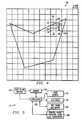
- FIGURE 4 illustrates the technique by which the present invention accomplishes the rendering of many gray shades while allowing for high resolution printing of stroke data.
- an array 64 of logical pixels is shown, as they would be mapped on a piece of paper. As an example, the size of these pixels is 1/300 of an inch.
- a polygon 66 is shown as printed on the array.
- Processors such as raster image processors, can be programmed to determine which pixels are inside of, outside of, or on the perimeter of a particular geometric shape.
- This technique known as scan conversion, has been described in Foley, et al., Computer Graphics: Principles and Practice, 2nd Edition , Addison-Wesley Publishing Company, 1992, pp. 92-94.
- this technique uses the geometric formula of an object, and pixel mapping, to determine whether a pixel is inside, outside, or on a shape.
- pixels within the polygon such as pixel 70
- pixels outside of the polygon such as pixel 72
- Pixels on the edge such as pixels 74 and 76
- pixels 74 and 76 will be treated as stroke data, and rendered at a high resolution, for example, a resolution of 1/600 of an inch, as discussed above.
- each 1/300 of an inch pixel is divided into smaller phases, for example, four 1/600 of an inch phases. Phases that fall outside the polygon, such as phase 78, will not be rendered. Phases within the polygon that do not fall on its perimeter, such as phase 80, will be rendered at a stroke gray scale as close to the desired gray scale as possible. As discussed previously, varying technologies offer between 8 and 32 shades of gray for high resolution pixels. Thus, the gray shade of phase 80 can be made as close as possible to the desired gray shades by reproducing the intensity level that best approximates the shade.
- Anti-aliasing techniques can also be used to determine the gray shades of the 1/300'' pixels and the 1/600'' phases. Such techniques are known in the art and have been described in Computer Graphics: Principles and Practice , pp. 132-134. Once the gray shade of a phase of a pixel on the perimeter is determined, it can be approximated through the use of lookup table B in FIGURE 3. As an example of an anti-aliasing technique, the percentage of the phase that is inside the perimeter of the polygon 66 is determined. This percentage is then multiplied by the desired gray scale to determine the gray scale to be rendered at the phase on the perimeter.
- phase 82 of polygon 66 is to be rendered at a gray level of 60, and assuming half of phase 82 is inside the polygon, then that phase can be rendered at 1 ⁇ 2 times 60, or 30. Using lookup table B in FIGURE 3, this translates to a desired intensity level of 7 at that phase.
- Phases other than A, B, E, and F can be used at the subpixel level on the perimeter to further smooth out jaggies as was discussed in copending U.S. Patent No. 5,453,778, "Method and Apparatus for Spatial Modulation in the Cross-Process Direction" (TI-17829) published as EP-A-0 636 997 (01/02/95).
- FIGURE 5 illustrates a block diagram of the circuitry for a printer 10 constructed according to the teachings of the present invention.
- a processor 100 receives data to be printed from block 102 either directly or through memory 104.
- Block 102 may represent any device that can output data to be printed, such as a personal computer.
- the memory 104 may be used to buffer data to be printed from block 102 or may store other data, such as pre-programmed data, for later printing.
- Memory 104 also includes instructions for controlling processor 100, as well as lookup tables, such as those discussed in connection with FIGURE 3.
- Processor 100 is coupled to light source 14, array 12, and OPC drum and motor 16.
- Processor 100 is also coupled to printer paper handling, user I/O, and diagnostics block 106.
- processor 100 processes the data to be printed by controlling light source 14 and array 12. For example, after determining that a pixel is to be contone data, processor 100 will determine the gray scale that must be written to that pixel, and with the aid of lookup tables controls the particular mirrors of array 12 and light source 14 to direct the appropriate intensity at different phases of the pixel. Processor 100 also controls the rotation of the OPC drum and the paper handling, user I/O and diagnostics as required by the printing system.
Description
- This invention relates generally to the field of printing, and more particularly to a method and apparatus for printing stroke and contone data together.
- Hard copy devices, such as printers, generally print two kinds of data. The first type of data is stroke data, usually text and graphics data. The second type of data is continuous tone ("contone") data, which is usually image data, for example, a data representation of a photographic image.
- High quality rendering of stroke data requires a printer that can produce a spatial resolution of 600 dots per inch ("dpi") or more. This resolution is required, for example, to reduce jaggedness of diagonal edges or to reproduce fine seriphs in text.
- Contone data, on the other hand, does not require such high spatial resolution, but requires a printer than can produce gray shades. Indeed, if the printer is capable of producing 256 gray shades (which is typical intensity resolution of image scanners), a 200-250 dpi printer will generally suffice. Such a printer provides appropriate spatial resolution for the human eye to perceive smooth shades.
- Unfortunately, most existing printers are binary printers that can reproduce only two gray shades, black and white. These printers simulate more gray shades by logically combining several dots into cells and relying on the spatial integration property of the human eye to stimulate smooth shades. As an example, a 3200 dpi printer can achieve appropriate gray shades by forming cells from 16
X 16 arrays of dots, resulting in 200 cells per inch (sometimes referred to as lines per inch). By controlling the number of dots that are black (or white) in this array, each cell can represent up to 257 gray levels (0 through 256, with 256 represented by all dots being black). The spatial resolution of the human eye will perceive smooth shades with such a printer. - Thus, binary printers reproduce high quality contone data only at an extremely high resolution. To produce both contone and stroke data, therefore, the resolution is defined by the contone image requirements. Consequently, the stroke data is printed at a higher resolution than needed. Furthermore, printing at the high resolution needed for contone data with existing systems makes them expensive.
- Therefore, a need has arisen for a printer that can print both stroke and contone data at the resolution of stroke data.
- EP-A-0 540 221 sets forth a printer using a laser scanning apparatus and discloses the idea of using "small pixels" within an "objective pixel" to achieve halftone printing. However, the pixels are not formed using a spatial light modulator array of elements.
- EP-A-0 361 880, which discloses an image signal processor, distinguishes between character data and halftone image data and applies an error diffusion process and binarisation process to the halftone image data and character data, respectively. This document is also directed to half-toning. The image signal processor comprises an image signal identification means for outputting a kind-identification signal of said input image signal based on a detected power at a fixed frequency at least in a direction of the main scanning or subscanning of the input image signal.
- EP-A-0 556 591 discloses a printer using an array of deformable mirror devices (DMD), a photoconductive drum and a processor for controlling the spatial light modulator such that predetermined areas of the photoconductive drum render gray scale levels.
- EP-A-0 620 676 discloses a process and architecture for a digital micromirror printer for achieving high resolution, high-speed gray scale printing with binary spatial light modulators. The process comprises illuminating a SLM having a plurality of rows of elements; using the SLM elements to modulate light in conjunction with movement of a photoconductive surface having a process direction, and converting grayscale information into codes that coordinate reflecting light from selected individual elements of the plurality of rows of said SLM with motion of the photoconductive surface, to reflect light on predetermined areas of the photoconductive surface that corresponds to that grayscale information. Additionaly, each pixel can be divided up into four phases in the process direction and printed in phase pairs.
- In accordance with the teaching of the present invention, a method and apparatus for printing stroke and contone data together is provided which substantially eliminates or reduces disadvantages and problems associated with prior art printers and printing techniques.
- According to the present invention, there is provided a method of printing both stroke and contone data as defined in
claim 1. - In particular, a method of printing both stroke and contone data together is disclosed in which data to be printed is identified as either contone data or stroke data. The contone data is then rendered with intensity modulation and spatial modulation in the process and cross-process directions, and the stroke data is rendered with intensity modulation. In a particular embodiment of the present invention, contone data is rendered by reflecting the light from predetermined individual elements of a plurality of rows onto predetermined phases of pixels of a photoconductive drum, the predetermined phases rendering the pixels at image quality gray scale levels. Stroke data is rendered by reflecting the light from predetermined individual elements onto predetermined phases of the photoconductive drum, the predetermined phases rendering the stroke data at high resolution.
- An important technical advantage of the present invention is that the different requirements of stroke and contone data are satisfied by using different methods to render them by exploiting spatial and intensity modulation capabilities of a DMD based printer.
- For a more complete understanding of the present invention, and the advantages thereof, reference is now made to the following descriptions taken in conjunction with the accompanying drawings, in which:
- FIGURE 1 illustrates a block diagram of a printer constructed according to the teachings of the present invention;
- FIGUREs 2a-2h illustrate various phases of a pixel to be printed according to present invention;
- FIGURE 3 illustrates lookup tables according to the teachings of the present invention;
- FIGURE 4 illustrates a polygon printed according to the teachings of the present invention; and
- FIGURE 5 illustrates a block diagram of the circuitry of a printer constructed according to the teachings of the present invention.
-
- FIGURE 1 illustrates a
printer 10 constructed according to the teachings of the present invention. As shown in FIGURE 1, a spatial light modulator (SLM) having individual elements making up anarray 12 is provided. In a particular embodiment,array 12 comprises an array of DMDs. Throughout this description, individual elements of thearray 12 will be referred to as mirrors.Array 12 may comprise an array of DMDs constructed as disclosed in U.S. Patent No. 4,956,619, "Spatial Light Modulator." - As shown in FIGURE 1, each row of
array 12 is staggered, such that individual mirrors (elements) are offset from row to row. This offset will be exploited, as discussed below, to allow for generation of many gray scales for the printing of image data and for the printing of smooth edges for graphics data. Only a portion ofarray 12 is shown for clarity, it being understood thatarray 12 may include more rows or columns, as particular applications require. - Light from a
light source 14 is reflected byarray 12 either onto or off ofOPC drum 16.Light source 14 may comprise a light-emitting diode. Light fromarray 12 may be reflected directly onto OPCdrum 16 or focused throughoptics 18. - As shown in FIGURE 1, light received from
array 12 falls onOPC drum 16. Only a line of logical pixels is shown for clarity, it being understood that several lines of pixels can be simultaneously illuminated by the DMD array. Each of these pixels will be illuminated and thereby either charged or discharged for toner attraction. Thedrum 16 will then rotate over the page to be printed, and the toner will be transferred from thedrum 16 to the page, the line of pixels printing a line on the page. - For the illustrated example, we will assume that the position (ON or OFF) of the mirrors in the array are updated for every one-quarter of a pixel drum movement. Other update speeds are possible, without departing from the scope of the invention. With this scheme, as shown in FIGURE 1, an
exemplary pixel 20 receives light from mirrors 22-36 ofarray 12. The light is received from each row of mirrors at different time instances as the drum rotates. Likewise, mirrors 38-52 reflect light ontopixel 54 ofOPC drum 16. Pixel 21 is also shown, and will be discussed below. Pixel 21 will be exposed by mirrors 22-36 asOPC drum 16 rotates. - FIGUREs 2a-2h illustrate light received at
pixel 20 from each of the mirrors 22-36. As shown in FIGURE 2a, light frommirrors pixel 20. In a particular embodiment, the mirrors ofarray 12 shine light on an area approximately ¼ the area ofpixel 20. For example,pixel 20 may be 1/300 of an inch by 1/300 of an inch, whereas the light frommirror 22 may be 1/600 of an inch by 1/600 of an inch. It should be understood that other sized and shaped pixels and mirrors are possible, or the effective size of the mirrors may be altered throughoptics 18. - The particular area on
pixel 20 on which light from any one mirror falls is referred to as a phase. Thus, as shown in FIGURE 2a, light frommirrors OPC drum 16 rotates, in this example by a quarter of a pixel, light frommirrors - As shown in FIGURE 2c, as
OPC drum 16 continues to rotate, light frommirrors mirrors pixel 20 and half on the adjacent pixel ofOPC drum 16. This light falling on the adjacent pixel can be handled in one of two ways. First, it can be taken into account in determining the gray scale to be generated in the adjacent pixel. Thus, if the gray scale of the adjacent pixel is to be, for example, level 200 of 256 gray levels, the amount of light received on that pixel from phase H can be taken into account. Alternatively, the light received from phase H on the adjacent pixel can be disregarded. Indeed, if the adjacent pixel is to be completely white, then this is the only alternative, and there will be some blur between pixels. - As shown in FIGURE 2d, as
OPC drum 16 continues to rotate, the light frommirrors OPC drum 16. This overlap can either be taken into account in determining the gray scale to be generated on that pixel, or disregarded. The light frommirrors - As shown in FIGURE 2e, as
OPC drum 16 continues to rotate, the light frommirrors mirrors mirrors mirrors mirrors - As shown in FIGURE 2g, light from
mirrors mirrors mirrors - Intensity modulation is achieved at each phase by choosing to turn the mirror ON or OFF (the ON position corresponds to the case where the light is reflected on the OPC pixel and the OFF position corresponds to the case where the light is reflected away from the OPC). As an example with the embodiment of FIGUREs 2a-2h, three levels of exposure may be generated for each phase by exposing each phase zero, one, or two times. For example, to generate an exposure level of one in phase A,
mirror 22 would be ON in FIGURE 2a, butmirror 30 would be OFF for FIGURE 2e. - More exposure levels are also possible by intensity modulation with amplitude modulation of the light source, which is, for example, an LED. For example, the entire array could be exposed at a certain base exposure level (1) for FIGUREs 2a-2d, and at twice that level (2) for FIGUREs 2e-2g. This cycle of intensity levels is repeated in a periodic fashion. With this scheme, four levels of exposure (0, 1, 2, and 3) can be generated in each phase. For example, to generate a level of 3 in phase A,
mirror 22 would be switched ON in FIGURE 2a andmirror 30 in FIGURE 2e. Many more exposure intensity levels can be generated by using more rows of DMDs and more light source levels. - Copending U.S. Patent No. 5,453,778, filed July 30, 1993, and entitled "Method and Apparatus for Spatial Modulation in the Cross-Process Direction," published as EP-A-636 997 (01/02/95), discloses in detail the techniques by which the apparatus of FIGURE 1 may be used to generate many shades of gray for the printing of contone data. As described in that application, the arrangement of
array 12 is exemplary, and other arrangements may also be used. Generally speaking, that application describes generating many shades of gray by integrating light from all of the phases of a particular pixel, with phase locations in both the process and cross-process directions. - Note that the size of a phase in the process direction is determined by the time the light source is ON when that phase is exposed. FIGUREs 2a-2g show the ideal case when the exposure is instantaneous. In the extreme case when the light source is on for the entire duration between two successive data load times, each phase will be about ¾ of a pixel wide, leading to overlap, for example between phases A and E. Thus, the size of the phases can also be varied or modulated for generating gray scales. This approach, referred to as pulse duration modulation, is described in copending U.S. Patent No. 5,461,411 filed March 29, 1993, entitled "Process and Architecture for Digital Micromirror Printer," (TI-17632) assigned to Texas Instruments Incorporated and published as EP-A-0 620 676 (19/10/94). Though the examples shown in this application show constant duration phases, it should be understood that the present invention may also use pulse duration modulation.
- With the present invention, contone data, as well as stroke data, can be printed together at different resolutions, thus allowing for the proper printing of both types of data. This is made possible by taking advantage of the fact that raster image processors ("RIPs") can distinguish between text and contone data. RIPs process printing languages, such as the postscript language, which require clear identification of different types of data, such as image data through use of the image operator, text data through use of the show operator, and graphics data through use of the stroke operator. Thus, with the present invention the RIP is programmed to render image data at a resolution which allows for the generation of many shades of gray, such as 300 dpi, while rendering text and graphics data at high resolution, such as 600 dpi. This is accomplished by taking advantage of the structure of
array 12, as will be discussed. - FIGURE 3 illustrates two lookup tables that are used by a RIP to render stroke and contone data. For contone data, lookup table A is used. Lookup table A provides the intensity levels that must fall on each phase of a pixel to generate the appropriate gray scale. The phases correspond to those of FIGUREs 2a-2h, and gray scale levels are rendered by integrating the light from the phases in both the process and cross-process directions.
Pixel 60 illustrates a pixel of contone data, for example, at 1/300 of an inch, to be printed at a gray scale level of 201. A raster image processor uses lookup table A to determine the particular light intensities that should fall on each of the phases ofpixel 60 to generate the gray scale level of 201. - In particular, to generate
gray scale 201 inpixel 60, the specific exposure levels desired for different phases are obtained through lookup table A. These tables can be derived experimentally or through modeling. The table entries are translated into mirror settings (ON or OFF) based on the light source intensity cycle. For example, assuming the light source is modulated periodically from one, to two, to four, to eight times a base intensity level, the mirrors that expose phase A may be ON for levels 2 and 8 and OFF forlevels 1 and 4 to generate a total intensity of 10 in phase A. - Stroke data is rendered through use of lookup table B, shown in FIGURE 3. Lookup table B provides the intensity level that must fall on a phase to render it at a particular gray shade. As illustrated,
pixel 62 is divided into four phases, phases A, B, E, and F, corresponding to the phases in FIGUREs 2a and 2c. These phases are of a resolution high enough to render high quality stroke data, for example, 1/600 of an inch. With existing optical photoconductive technology, dots of the size of about 1/600 of an inch can be rendered at about 8-32 shades of gray. Thus, the intensity required to generate the appropriate shades of gray for phases A, B, E, and F, can be obtained from lookup table B. Thus, for example, if phase A were to be rendered at a gray scale level of 30, an intensity level of, for example, 7 would be directed to that phase. Likewise, if phase F is to be at a gray scale of 100, an intensity level of 15 would be directed to that phase. Although 256 gray shades index into the lookup table B, fewer intensity levels are output from the lookup table due to the above mentioned toner limitations. - In the example described for stroke data, the stroke data is rendered by using the four phases A, B, E, and F of
pixel 62. With such an arrangement, the other phases ofpixel 62 are inactive, and stroke data is rendered at twice the spatial resolution of contone data. This arrangement is shown for convenience, it being understood that other arrangements are also possible. As discussed above, for example,pixel 62 can include many other phases, for example phases C, D, and G-P. With the present invention, any of these phases may be used to render the stroke data. By using phases other than just phases A, B, E, and F, the stroke data will be rendered at the same overall resolution, but can be addressed at a finer resolution, due to the offset of the rows ofarray 12. This fine addressing is discussed in "Method and Apparatus for Spatial Modulation in the Cross-Process Direction." Furthermore, it should be understood that the present invention works without staggering of the rows ofarray 12. It should be noted that dithering or half-toning schemes can be used in conjunction with the above methods, in particular for rendering stroke data which does not exploit spatial modulation. - Some input contone data may be received at 600 dpi resolution, and such contone data can be handled in at least three ways to generate gray shades. In one alternative, the 600 dpi contone data can be rendered through use of lookup table B, and use of the four phases shown in connection with
pixel 62 of FIGURE 3, which may also be combined with some dithering scheme. Second, the gray scale of each of the 600 dpi data points can be averaged and then rendered through use of a lookup table such as lookup table A. For example, if the contone data is received at 600 dpi, then there are four data points for each 1/300 of an inch pixel. The gray scale for each of these four data points can be averaged (for example, arithmetically) to derive a gray scale for the 1/300 of an inch pixel. This averaged gray scale can then be rendered through use of lookup table A, as discussed above. As a third alternative, this data can be subsampled by half (after smoothing with a low pass filter to prevent aliasing) to 300 dpi resolution, and rendered through use of lookup table A. - Many applications require both high resolution and many shades of gray. An example is the printing of graphics data, such as that for geometric shapes with a solid, patterned, or gradient fill. It is desirable to allow the rendering of many shades of gray within the geometric shape, while providing high resolution at the edges to prevent jagged appearing edges. The above discussion describes how contone and stroke data, once identified as such, are handled by the RIP, the
array 12, and theOPC drum 16. Following is a discussion of how the data is so identified, and then printed. - FIGURE 4 illustrates the technique by which the present invention accomplishes the rendering of many gray shades while allowing for high resolution printing of stroke data. As shown in FIGURE 4, an
array 64 of logical pixels is shown, as they would be mapped on a piece of paper. As an example, the size of these pixels is 1/300 of an inch. Apolygon 66 is shown as printed on the array. Processors, such as raster image processors, can be programmed to determine which pixels are inside of, outside of, or on the perimeter of a particular geometric shape. This technique, known as scan conversion, has been described in Foley, et al., Computer Graphics: Principles and Practice, 2nd Edition, Addison-Wesley Publishing Company, 1992, pp. 92-94. Generally speaking, this technique uses the geometric formula of an object, and pixel mapping, to determine whether a pixel is inside, outside, or on a shape. - Thus, pixels within the polygon, such as
pixel 70, will be treated as if they were contone data, and printed as discussed above, for example using 16 phases. Likewise, pixels outside of the polygon, such aspixel 72, will not be rendered. Pixels on the edge, such aspixels - To accomplish this high resolution rendering with the present invention, each 1/300 of an inch pixel is divided into smaller phases, for example, four 1/600 of an inch phases. Phases that fall outside the polygon, such as
phase 78, will not be rendered. Phases within the polygon that do not fall on its perimeter, such asphase 80, will be rendered at a stroke gray scale as close to the desired gray scale as possible. As discussed previously, varying technologies offer between 8 and 32 shades of gray for high resolution pixels. Thus, the gray shade ofphase 80 can be made as close as possible to the desired gray shades by reproducing the intensity level that best approximates the shade. - Anti-aliasing techniques can also be used to determine the gray shades of the 1/300'' pixels and the 1/600'' phases. Such techniques are known in the art and have been described in Computer Graphics: Principles and Practice, pp. 132-134. Once the gray shade of a phase of a pixel on the perimeter is determined, it can be approximated through the use of lookup table B in FIGURE 3. As an example of an anti-aliasing technique, the percentage of the phase that is inside the perimeter of the
polygon 66 is determined. This percentage is then multiplied by the desired gray scale to determine the gray scale to be rendered at the phase on the perimeter. For example, ifphase 82 ofpolygon 66 is to be rendered at a gray level of 60, and assuming half ofphase 82 is inside the polygon, then that phase can be rendered at ½times - Phases other than A, B, E, and F can be used at the subpixel level on the perimeter to further smooth out jaggies as was discussed in copending U.S. Patent No. 5,453,778, "Method and Apparatus for Spatial Modulation in the Cross-Process Direction" (TI-17829) published as EP-A-0 636 997 (01/02/95).
- FIGURE 5 illustrates a block diagram of the circuitry for a
printer 10 constructed according to the teachings of the present invention. As shown in FIGURE 5, aprocessor 100 receives data to be printed fromblock 102 either directly or throughmemory 104.Block 102 may represent any device that can output data to be printed, such as a personal computer. Thememory 104 may be used to buffer data to be printed fromblock 102 or may store other data, such as pre-programmed data, for later printing.Memory 104 also includes instructions for controllingprocessor 100, as well as lookup tables, such as those discussed in connection with FIGURE 3.Processor 100 is coupled tolight source 14,array 12, and OPC drum andmotor 16.Processor 100 is also coupled to printer paper handling, user I/O, and diagnostics block 106. - In operation,
processor 100 processes the data to be printed by controllinglight source 14 andarray 12. For example, after determining that a pixel is to be contone data,processor 100 will determine the gray scale that must be written to that pixel, and with the aid of lookup tables controls the particular mirrors ofarray 12 andlight source 14 to direct the appropriate intensity at different phases of the pixel.Processor 100 also controls the rotation of the OPC drum and the paper handling, user I/O and diagnostics as required by the printing system. - Although the present invention has been described in detail, it should be understood that various changes, substitutions, and alterations can be made without departing from the scope of the appended claims.
Claims (6)
- A method of printing both stroke and contone data comprising:illuminating a spatial light modulator (12) having a plurality of rows of elements (22-36, 38-52);using said spatial light modulator elements (22-36, 38-52) to modulate light in conjunction with movement of a photoconductive surface (16) having a process direction;for the contone data, coordinating the reflection of light from selected individual elements (22-36, 38-52) of said plurality of rows of said spatial light modulator (12) with motion of said photoconductive surface (16), to reflect light on predetermined areas of said photoconductive surface (16) to form a contone data pixel that corresponds to that grayscale information;attracting toner to the areas, the amount of toner attracted to a particular area being based on the amount of light that has fallen on that area; andtransferring the toner to a print medium;
whereinsaid modulation is performed by said spatial light modulator elements (22-36, 38-52) in both the process and cross process directions andfor the stroke data, reflecting light from predetermined individual elements (22-36, 38-52) onto phases of a pixel (62), wherein each phase of a pixel (62) is an area that is smaller than the area of a printed contone data pixel (60), wherein the placement of the areas is controlled to produce a resolution higher than the resolution of the printed contone data pixels (60), and intensity modulating the stroke data using said light source (14) illuminating the spatial light modulator elements (22-36, 38-52) to control the amount of illumination modulated by said elements (22-36, 38-52) to form a print image with the stroke data. - The method of claim 1, further comprising producing the stroke data at each pixel (62) by reflecting light onto fewer than all of the phases of a pixel (62).
- The method of claim 1, further comprising using staggered rows of elements of the spatial light modulator (12), and timing illumination of those rows with the rotation of the photoconductive surface (16) to provide at least two phases for each pixel (60) in the cross process direction.
- The method of any of claims 1 to 3, wherein said step of illuminating comprises pulsing the light such that each individual element (22-36, 38-52) is operable to reflect light on at least two area locations in the process direction.
- The method of any of claims 1 to 4, and further comprising the step of periodically changing the intensity of the light.
- The method of any of claims 1 to 5, wherein said step of reflecting comprises switching the individual elements (22-36, 38-52) such that each individual element (22-36, 38-52) is operable to reflect light on at least two areas in the process direction.
Priority Applications (1)
| Application Number | Priority Date | Filing Date | Title |
|---|---|---|---|
| EP98114020A EP0875386B1 (en) | 1993-08-30 | 1994-08-25 | Improvements in or relating to printing |
Applications Claiming Priority (2)
| Application Number | Priority Date | Filing Date | Title |
|---|---|---|---|
| US08/113,936 US5459492A (en) | 1993-08-30 | 1993-08-30 | Method and apparatus for printing stroke and contone data together |
| US113936 | 1993-08-30 |
Related Child Applications (1)
| Application Number | Title | Priority Date | Filing Date |
|---|---|---|---|
| EP98114020A Division EP0875386B1 (en) | 1993-08-30 | 1994-08-25 | Improvements in or relating to printing |
Publications (3)
| Publication Number | Publication Date |
|---|---|
| EP0640488A2 EP0640488A2 (en) | 1995-03-01 |
| EP0640488A3 EP0640488A3 (en) | 1996-01-24 |
| EP0640488B1 true EP0640488B1 (en) | 1999-04-21 |
Family
ID=22352402
Family Applications (2)
| Application Number | Title | Priority Date | Filing Date |
|---|---|---|---|
| EP98114020A Expired - Lifetime EP0875386B1 (en) | 1993-08-30 | 1994-08-25 | Improvements in or relating to printing |
| EP94113311A Expired - Lifetime EP0640488B1 (en) | 1993-08-30 | 1994-08-25 | Improvements in or relating to printing |
Family Applications Before (1)
| Application Number | Title | Priority Date | Filing Date |
|---|---|---|---|
| EP98114020A Expired - Lifetime EP0875386B1 (en) | 1993-08-30 | 1994-08-25 | Improvements in or relating to printing |
Country Status (6)
| Country | Link |
|---|---|
| US (1) | US5459492A (en) |
| EP (2) | EP0875386B1 (en) |
| JP (1) | JPH07232458A (en) |
| KR (1) | KR100313410B1 (en) |
| DE (2) | DE69431078T2 (en) |
| TW (1) | TW367691B (en) |
Families Citing this family (40)
| Publication number | Priority date | Publication date | Assignee | Title |
|---|---|---|---|---|
| US6219015B1 (en) | 1992-04-28 | 2001-04-17 | The Board Of Directors Of The Leland Stanford, Junior University | Method and apparatus for using an array of grating light valves to produce multicolor optical images |
| US5754217A (en) * | 1995-04-19 | 1998-05-19 | Texas Instruments Incorporated | Printing system and method using a staggered array spatial light modulator having masked mirror elements |
| US5841579A (en) | 1995-06-07 | 1998-11-24 | Silicon Light Machines | Flat diffraction grating light valve |
| US5699168A (en) * | 1995-06-22 | 1997-12-16 | Texas Instruments Incorporated | Grayscale printing with sliding window memory |
| US5982553A (en) | 1997-03-20 | 1999-11-09 | Silicon Light Machines | Display device incorporating one-dimensional grating light-valve array |
| US6088102A (en) | 1997-10-31 | 2000-07-11 | Silicon Light Machines | Display apparatus including grating light-valve array and interferometric optical system |
| JPH11320968A (en) * | 1998-05-13 | 1999-11-24 | Ricoh Microelectronics Co Ltd | Optical image forming method and apparatus, imaging system and exposing unit for lithography |
| US6271808B1 (en) | 1998-06-05 | 2001-08-07 | Silicon Light Machines | Stereo head mounted display using a single display device |
| US6130770A (en) | 1998-06-23 | 2000-10-10 | Silicon Light Machines | Electron gun activated grating light valve |
| US6101036A (en) | 1998-06-23 | 2000-08-08 | Silicon Light Machines | Embossed diffraction grating alone and in combination with changeable image display |
| US6215579B1 (en) | 1998-06-24 | 2001-04-10 | Silicon Light Machines | Method and apparatus for modulating an incident light beam for forming a two-dimensional image |
| US6303986B1 (en) | 1998-07-29 | 2001-10-16 | Silicon Light Machines | Method of and apparatus for sealing an hermetic lid to a semiconductor die |
| US6429949B1 (en) | 1998-10-15 | 2002-08-06 | Electronics For Imaging, Inc. | Low memory printer controller |
| US6487322B1 (en) * | 1999-03-03 | 2002-11-26 | Autodesk Canada Inc. | Generating image data |
| DE10012017A1 (en) | 2000-03-11 | 2001-09-13 | Basysprint Gmbh Sys Druckind | Printing plate exposure device, has optical error and/or tolerance compensation device incorporated in electronic image processing device controlling light modulator |
| US6396530B1 (en) * | 2000-06-12 | 2002-05-28 | Eastman Kodak Company | Method for improving exposure resolution using multiple exposures |
| JP3512171B2 (en) * | 2000-08-28 | 2004-03-29 | 大日本スクリーン製造株式会社 | Image recording device |
| JP4497682B2 (en) * | 2000-09-01 | 2010-07-07 | キヤノン株式会社 | Image forming apparatus |
| US6707591B2 (en) | 2001-04-10 | 2004-03-16 | Silicon Light Machines | Angled illumination for a single order light modulator based projection system |
| US6782205B2 (en) | 2001-06-25 | 2004-08-24 | Silicon Light Machines | Method and apparatus for dynamic equalization in wavelength division multiplexing |
| US6747781B2 (en) | 2001-06-25 | 2004-06-08 | Silicon Light Machines, Inc. | Method, apparatus, and diffuser for reducing laser speckle |
| US6829092B2 (en) | 2001-08-15 | 2004-12-07 | Silicon Light Machines, Inc. | Blazed grating light valve |
| TW556043B (en) | 2001-11-30 | 2003-10-01 | Asml Netherlands Bv | Imaging apparatus, device manufacturing method and device manufactured by said method |
| US6800238B1 (en) | 2002-01-15 | 2004-10-05 | Silicon Light Machines, Inc. | Method for domain patterning in low coercive field ferroelectrics |
| US6767751B2 (en) | 2002-05-28 | 2004-07-27 | Silicon Light Machines, Inc. | Integrated driver process flow |
| US6728023B1 (en) | 2002-05-28 | 2004-04-27 | Silicon Light Machines | Optical device arrays with optimized image resolution |
| US6822797B1 (en) | 2002-05-31 | 2004-11-23 | Silicon Light Machines, Inc. | Light modulator structure for producing high-contrast operation using zero-order light |
| US6829258B1 (en) | 2002-06-26 | 2004-12-07 | Silicon Light Machines, Inc. | Rapidly tunable external cavity laser |
| US6813059B2 (en) | 2002-06-28 | 2004-11-02 | Silicon Light Machines, Inc. | Reduced formation of asperities in contact micro-structures |
| US6801354B1 (en) | 2002-08-20 | 2004-10-05 | Silicon Light Machines, Inc. | 2-D diffraction grating for substantially eliminating polarization dependent losses |
| KR101049608B1 (en) * | 2002-08-24 | 2011-07-14 | 매스크리스 리소그래피 인코퍼레이티드 | Continuous Direct-Write Optical Lithography Apparatus and Method |
| US6712480B1 (en) | 2002-09-27 | 2004-03-30 | Silicon Light Machines | Controlled curvature of stressed micro-structures |
| US8045215B2 (en) * | 2002-10-18 | 2011-10-25 | Hewlett-Packard Development Company, L.P. | Printer object list resolutions |
| US7042622B2 (en) * | 2003-10-30 | 2006-05-09 | Reflectivity, Inc | Micromirror and post arrangements on substrates |
| US6829077B1 (en) | 2003-02-28 | 2004-12-07 | Silicon Light Machines, Inc. | Diffractive light modulator with dynamically rotatable diffraction plane |
| US6806997B1 (en) | 2003-02-28 | 2004-10-19 | Silicon Light Machines, Inc. | Patterned diffractive light modulator ribbon for PDL reduction |
| KR20050077756A (en) * | 2004-01-28 | 2005-08-03 | 이 아이 듀폰 디 네모아 앤드 캄파니 | Method for imaging regular patterns |
| US8335999B2 (en) | 2010-06-11 | 2012-12-18 | Orbotech Ltd. | System and method for optical shearing |
| US10872257B2 (en) * | 2018-06-06 | 2020-12-22 | Weltrend Semiconductor Inc. | Barcode detection method and barcode detection system for increasing detection efficiency |
| TWI676936B (en) * | 2018-06-06 | 2019-11-11 | 偉詮電子股份有限公司 | Barcode detection method and barcode detection system |
Citations (1)
| Publication number | Priority date | Publication date | Assignee | Title |
|---|---|---|---|---|
| EP0620676A1 (en) * | 1993-03-29 | 1994-10-19 | Agfa-Gevaert N.V. | Process and architecture for digital micromirror printer |
Family Cites Families (14)
| Publication number | Priority date | Publication date | Assignee | Title |
|---|---|---|---|---|
| US4577235A (en) * | 1984-08-20 | 1986-03-18 | The Mead Corporation | Text/continuous tone image decision processor |
| US4677571A (en) * | 1985-02-08 | 1987-06-30 | Rise Technology Inc. | Electronic publishing |
| US4838652A (en) * | 1985-05-15 | 1989-06-13 | Canon Kabushiki Kaisha | Image forming apparatus |
| US4673953A (en) * | 1985-12-13 | 1987-06-16 | Xerox Corporation | Interpixel null suppression for optical image bars |
| US4956619A (en) * | 1988-02-19 | 1990-09-11 | Texas Instruments Incorporated | Spatial light modulator |
| JPH0296473A (en) * | 1988-09-30 | 1990-04-09 | Matsushita Graphic Commun Syst Inc | Picture signal processor |
| US4965599A (en) * | 1989-11-13 | 1990-10-23 | Eastman Kodak Company | Scanning apparatus for halftone image screen writing |
| US5142303A (en) * | 1989-12-21 | 1992-08-25 | Texas Instruments Incorporated | Printing system exposure module optic structure and method of operation |
| US5049901A (en) * | 1990-07-02 | 1991-09-17 | Creo Products Inc. | Light modulator using large area light sources |
| US5225911A (en) * | 1991-05-07 | 1993-07-06 | Xerox Corporation | Means for combining data of different frequencies for a raster output device |
| US5185852A (en) * | 1991-05-31 | 1993-02-09 | Digital Equipment Corporation | Antialiasing apparatus and method for computer printers |
| US5223857A (en) * | 1991-09-09 | 1993-06-29 | Xerox Corporation | Pulsed imaging, pulse width modulation raster output scanner for tri-level exposure |
| DE69227886T2 (en) * | 1991-11-01 | 1999-06-10 | Konishiroku Photo Ind | Imaging device |
| CA2087625C (en) * | 1992-01-23 | 2006-12-12 | William E. Nelson | Non-systolic time delay and integration printing |
-
1993
- 1993-08-30 US US08/113,936 patent/US5459492A/en not_active Expired - Fee Related
-
1994
- 1994-08-25 EP EP98114020A patent/EP0875386B1/en not_active Expired - Lifetime
- 1994-08-25 DE DE69431078T patent/DE69431078T2/en not_active Expired - Fee Related
- 1994-08-25 EP EP94113311A patent/EP0640488B1/en not_active Expired - Lifetime
- 1994-08-25 DE DE69417973T patent/DE69417973T2/en not_active Expired - Fee Related
- 1994-08-29 JP JP6203769A patent/JPH07232458A/en not_active Ceased
- 1994-08-29 KR KR1019940021353A patent/KR100313410B1/en not_active IP Right Cessation
- 1994-09-02 TW TW083108070A patent/TW367691B/en not_active IP Right Cessation
Patent Citations (1)
| Publication number | Priority date | Publication date | Assignee | Title |
|---|---|---|---|---|
| EP0620676A1 (en) * | 1993-03-29 | 1994-10-19 | Agfa-Gevaert N.V. | Process and architecture for digital micromirror printer |
Also Published As
| Publication number | Publication date |
|---|---|
| JPH07232458A (en) | 1995-09-05 |
| TW367691B (en) | 1999-08-21 |
| DE69417973D1 (en) | 1999-05-27 |
| DE69431078T2 (en) | 2003-01-30 |
| KR100313410B1 (en) | 2002-04-24 |
| US5459492A (en) | 1995-10-17 |
| EP0875386A1 (en) | 1998-11-04 |
| DE69417973T2 (en) | 1999-10-07 |
| EP0640488A3 (en) | 1996-01-24 |
| EP0875386B1 (en) | 2002-07-24 |
| EP0640488A2 (en) | 1995-03-01 |
| DE69431078D1 (en) | 2002-08-29 |
| KR950006653A (en) | 1995-03-21 |
Similar Documents
| Publication | Publication Date | Title |
|---|---|---|
| EP0640488B1 (en) | Improvements in or relating to printing | |
| KR100245235B1 (en) | System and method for achieving gray scale dmd operation | |
| EP0636997B1 (en) | Spatial light modulation | |
| JP2583717B2 (en) | Display device with fine position designation | |
| EP0620676B1 (en) | Process for digital micromirror printer | |
| US5742703A (en) | Method and apparatus for the resolution enhancement of gray-scale images that include text and line art | |
| KR100318033B1 (en) | Grayscale Printing with Spatial Light Modulators | |
| US5430472A (en) | Method and apparatus for eliminating distortion via overscanned illumination for optical printers and the like having high gamma photosensitive recording media and high addressability | |
| EP0854636B1 (en) | Hierarchical template-matching filters | |
| EP1426900B1 (en) | Image forming apparatus with resolution conversion | |
| US5357273A (en) | Resolution conversion via intensity controlled overscanned illumination for optical printers and the like having high gamma photosensitive recording media | |
| US5367381A (en) | Method and apparatus for enhanced resolution and contrast via super intensity controlled overscanned illumination in a two dimensional high addressability printer | |
| US6295078B1 (en) | Methods of providing lower resolution format data into a higher resolution format | |
| JP2002356008A (en) | Image forming apparatus and method | |
| US5841956A (en) | Anti-aliasing for digital printing with dot shape modulation and greyscale | |
| CA2134517C (en) | Multi-level xerography exposure control through multi-beam overscan | |
| JPH0862911A (en) | Method and apparatus for spatial light modulation | |
| JPH0691930A (en) | Method and device for improving resolution and contrast of optical printer | |
| JPH03206478A (en) | Laser scanning type image forming device | |
| WO1995033330A1 (en) | Technique for rendering images on a binary marking engine |
Legal Events
| Date | Code | Title | Description |
|---|---|---|---|
| PUAI | Public reference made under article 153(3) epc to a published international application that has entered the european phase |
Free format text: ORIGINAL CODE: 0009012 |
|
| AK | Designated contracting states |
Kind code of ref document: A2 Designated state(s): DE FR GB IT NL |
|
| PUAL | Search report despatched |
Free format text: ORIGINAL CODE: 0009013 |
|
| AK | Designated contracting states |
Kind code of ref document: A3 Designated state(s): DE FR GB IT NL |
|
| 17P | Request for examination filed |
Effective date: 19960605 |
|
| 17Q | First examination report despatched |
Effective date: 19970403 |
|
| GRAG | Despatch of communication of intention to grant |
Free format text: ORIGINAL CODE: EPIDOS AGRA |
|
| GRAG | Despatch of communication of intention to grant |
Free format text: ORIGINAL CODE: EPIDOS AGRA |
|
| GRAG | Despatch of communication of intention to grant |
Free format text: ORIGINAL CODE: EPIDOS AGRA |
|
| GRAH | Despatch of communication of intention to grant a patent |
Free format text: ORIGINAL CODE: EPIDOS IGRA |
|
| GRAH | Despatch of communication of intention to grant a patent |
Free format text: ORIGINAL CODE: EPIDOS IGRA |
|
| GRAA | (expected) grant |
Free format text: ORIGINAL CODE: 0009210 |
|
| ITF | It: translation for a ep patent filed |
Owner name: BARZANO' E ZANARDO ROMA S.P.A. |
|
| AK | Designated contracting states |
Kind code of ref document: B1 Designated state(s): DE FR GB IT NL |
|
| REF | Corresponds to: |
Ref document number: 69417973 Country of ref document: DE Date of ref document: 19990527 |
|
| ET | Fr: translation filed | ||
| PLBE | No opposition filed within time limit |
Free format text: ORIGINAL CODE: 0009261 |
|
| STAA | Information on the status of an ep patent application or granted ep patent |
Free format text: STATUS: NO OPPOSITION FILED WITHIN TIME LIMIT |
|
| 26N | No opposition filed | ||
| REG | Reference to a national code |
Ref country code: GB Ref legal event code: IF02 |
|
| PGFP | Annual fee paid to national office [announced via postgrant information from national office to epo] |
Ref country code: IT Payment date: 20060831 Year of fee payment: 13 |
|
| PGFP | Annual fee paid to national office [announced via postgrant information from national office to epo] |
Ref country code: NL Payment date: 20080715 Year of fee payment: 15 Ref country code: DE Payment date: 20080829 Year of fee payment: 15 |
|
| PGFP | Annual fee paid to national office [announced via postgrant information from national office to epo] |
Ref country code: FR Payment date: 20080807 Year of fee payment: 15 |
|
| PGFP | Annual fee paid to national office [announced via postgrant information from national office to epo] |
Ref country code: GB Payment date: 20080708 Year of fee payment: 15 |
|
| PG25 | Lapsed in a contracting state [announced via postgrant information from national office to epo] |
Ref country code: IT Free format text: LAPSE BECAUSE OF NON-PAYMENT OF DUE FEES Effective date: 20070825 |
|
| REG | Reference to a national code |
Ref country code: NL Ref legal event code: V1 Effective date: 20100301 |
|
| GBPC | Gb: european patent ceased through non-payment of renewal fee |
Effective date: 20090825 |
|
| REG | Reference to a national code |
Ref country code: FR Ref legal event code: ST Effective date: 20100430 |
|
| PG25 | Lapsed in a contracting state [announced via postgrant information from national office to epo] |
Ref country code: NL Free format text: LAPSE BECAUSE OF NON-PAYMENT OF DUE FEES Effective date: 20100301 Ref country code: FR Free format text: LAPSE BECAUSE OF NON-PAYMENT OF DUE FEES Effective date: 20090831 Ref country code: DE Free format text: LAPSE BECAUSE OF NON-PAYMENT OF DUE FEES Effective date: 20100302 |
|
| PG25 | Lapsed in a contracting state [announced via postgrant information from national office to epo] |
Ref country code: GB Free format text: LAPSE BECAUSE OF NON-PAYMENT OF DUE FEES Effective date: 20090825 |