EP0653710B1 - Speech information processing - Google Patents
Speech information processing Download PDFInfo
- Publication number
- EP0653710B1 EP0653710B1 EP94307883A EP94307883A EP0653710B1 EP 0653710 B1 EP0653710 B1 EP 0653710B1 EP 94307883 A EP94307883 A EP 94307883A EP 94307883 A EP94307883 A EP 94307883A EP 0653710 B1 EP0653710 B1 EP 0653710B1
- Authority
- EP
- European Patent Office
- Prior art keywords
- speech information
- execution means
- sound source
- memory
- memory means
- Prior art date
- Legal status (The legal status is an assumption and is not a legal conclusion. Google has not performed a legal analysis and makes no representation as to the accuracy of the status listed.)
- Expired - Lifetime
Links
- 230000010365 information processing Effects 0.000 title description 4
- 230000015654 memory Effects 0.000 claims description 136
- 230000004044 response Effects 0.000 claims description 3
- 239000011295 pitch Substances 0.000 description 18
- 239000000654 additive Substances 0.000 description 15
- 230000000996 additive effect Effects 0.000 description 15
- 238000006243 chemical reaction Methods 0.000 description 11
- 238000000034 method Methods 0.000 description 7
- 238000010586 diagram Methods 0.000 description 5
- 238000004519 manufacturing process Methods 0.000 description 5
- 238000005070 sampling Methods 0.000 description 5
- 238000001514 detection method Methods 0.000 description 4
- 230000003252 repetitive effect Effects 0.000 description 4
- 238000013500 data storage Methods 0.000 description 2
- 230000000694 effects Effects 0.000 description 2
- 230000002269 spontaneous effect Effects 0.000 description 2
- 230000006835 compression Effects 0.000 description 1
- 238000007906 compression Methods 0.000 description 1
- 230000003247 decreasing effect Effects 0.000 description 1
- 230000009977 dual effect Effects 0.000 description 1
- 238000005562 fading Methods 0.000 description 1
- 230000003993 interaction Effects 0.000 description 1
- 238000013139 quantization Methods 0.000 description 1
- 239000010453 quartz Substances 0.000 description 1
- 238000009877 rendering Methods 0.000 description 1
- VYPSYNLAJGMNEJ-UHFFFAOYSA-N silicon dioxide Inorganic materials O=[Si]=O VYPSYNLAJGMNEJ-UHFFFAOYSA-N 0.000 description 1
- 230000003936 working memory Effects 0.000 description 1
Images


Classifications
-
- G—PHYSICS
- G10—MUSICAL INSTRUMENTS; ACOUSTICS
- G10H—ELECTROPHONIC MUSICAL INSTRUMENTS; INSTRUMENTS IN WHICH THE TONES ARE GENERATED BY ELECTROMECHANICAL MEANS OR ELECTRONIC GENERATORS, OR IN WHICH THE TONES ARE SYNTHESISED FROM A DATA STORE
- G10H7/00—Instruments in which the tones are synthesised from a data store, e.g. computer organs
- G10H7/002—Instruments in which the tones are synthesised from a data store, e.g. computer organs using a common processing for different operations or calculations, and a set of microinstructions (programme) to control the sequence thereof
- G10H7/004—Instruments in which the tones are synthesised from a data store, e.g. computer organs using a common processing for different operations or calculations, and a set of microinstructions (programme) to control the sequence thereof with one or more auxiliary processor in addition to the main processing unit
-
- G—PHYSICS
- G10—MUSICAL INSTRUMENTS; ACOUSTICS
- G10H—ELECTROPHONIC MUSICAL INSTRUMENTS; INSTRUMENTS IN WHICH THE TONES ARE GENERATED BY ELECTROMECHANICAL MEANS OR ELECTRONIC GENERATORS, OR IN WHICH THE TONES ARE SYNTHESISED FROM A DATA STORE
- G10H7/00—Instruments in which the tones are synthesised from a data store, e.g. computer organs
- G10H7/08—Instruments in which the tones are synthesised from a data store, e.g. computer organs by calculating functions or polynomial approximations to evaluate amplitudes at successive sample points of a tone waveform
-
- G—PHYSICS
- G06—COMPUTING; CALCULATING OR COUNTING
- G06F—ELECTRIC DIGITAL DATA PROCESSING
- G06F13/00—Interconnection of, or transfer of information or other signals between, memories, input/output devices or central processing units
- G06F13/14—Handling requests for interconnection or transfer
- G06F13/16—Handling requests for interconnection or transfer for access to memory bus
- G06F13/1668—Details of memory controller
- G06F13/1673—Details of memory controller using buffers
-
- G—PHYSICS
- G10—MUSICAL INSTRUMENTS; ACOUSTICS
- G10L—SPEECH ANALYSIS OR SYNTHESIS; SPEECH RECOGNITION; SPEECH OR VOICE PROCESSING; SPEECH OR AUDIO CODING OR DECODING
- G10L13/00—Speech synthesis; Text to speech systems
- G10L13/02—Methods for producing synthetic speech; Speech synthesisers
- G10L13/04—Details of speech synthesis systems, e.g. synthesiser structure or memory management
Definitions
- This invention relates to a speech information processor which may, for example, advantageously be employed in an electronic musical instrument or a television game device.
- the sound sources employed in general in an electronic musical instrument or a television game may be roughly classified into analog sound sources, comprising a voltage-controlled oscillator (VCO), a voltage-controlled amplifier (VCA), a voltage-controlled filter (VCF) etc., and digital sound sources, such as a programmable sound generator (PSG) or a zigzag readout type ROM.
- VCO voltage-controlled oscillator
- VCA voltage-controlled amplifier
- VCF voltage-controlled filter
- digital sound sources such as a programmable sound generator (PSG) or a zigzag readout type ROM.
- JP-A-62264099 (1987) or JP-A-62267798 (1987) disclose a sampler sound source in which sound source data sampled from live instrument sound and digitally processed is stored in a memory for use as a sound source.
- the above-mentioned sound source stores only sound source data of a pre-set pitch (interval) after compression by, for example, non-linear quantization.
- Each sound source data is stored in two parts, that is in a formant portion (FR) and a one-period portion (LP) of plural repeated waveforms of the fundamental period following the formant portion, as shown in Fig.4.
- the formant portion is a signal waveform at the initial stage of sound production proper to each musical instrument, such as a sound produced from when a key of a keyboard is struck until a hammer hits the string in the case of a piano.
- the formant portion is read out first and the one-period portion is read out a plurality of times.
- an audio processing unit (APU) 107 consisting of a digital signal processing unit (DSP) 101, a memory 102 and a central processing unit (CPU) 103, as shown in Fig.10, has been proposed.
- DSP digital signal processing unit
- CPU central processing unit
- the APU 107 is connected to a host computer 104, provided in a customary personal computer, a digital electronic musical instrument or a TV game machine.
- the host computer 104 includes a ROM cassette storing the above-mentioned sound source data, control programs, etc.
- the control program stored in the ROM cassette is read out by the CPU 103 so as to be stored in a working memory (RAM) 103a therein.
- the CPU 103 causes the sound source data to be read out from the ROM cassette and transiently stored in the memory 102 via the DSP 101, based upon the above-mentioned control program by way of performing writing control for the memory 102.
- the CPU 103 also controls the DSP 101 in accordance with the control program.
- the DSP 101 causes the sound source data stored in the memory 102 to be read out under control by the CPU 103 and processes the sound source data thus read out with, for example, bit expansion or pitch conversion.
- the DSP 101 also processes the sound source data with looping for reading out the repetitive portion of the sound source data a plurality of number of times.
- the sound source data outputted by the DSP 101 after such processing operations, is fed by a D/A converter 105 and thereby converted into analog speech signals which are fed to a speaker unit 106.
- a D/A converter 105 converts analog speech signals into analog speech signals into analog speech signals into analog speech signals into analog speech signals into a speaker unit 106.
- an acoustic output corresponding to the speech sound data can be produced via the speaker unit 106.
- the access timing to the memory 102 by the CPU 103 and the DSP 101 is pre-set so that the CPU 101 accesses the memory 102 once after the DSP 101 accesses the memory twice. Consequently, when partially rewriting the sound source data of the memory 102, the CPU 103 controls the writing in the memory 102 so that the CPU reads out sound source data from the ROM cassette and writes the data in the memory 102 during the time the DSP 101 is not accessing the memory. This enables the acoustic output corresponding to the rewritten scund source data to be produced from the next time on.
- the present applicants have filed a related European Application Publication No. EP-A-0 543 667 and corresponding US Patent Nos. US-A-5 390 158 and US-A-5 539 716.
- the memory 102 is used in common by the DSP 101 and the CPU 103, and the access timing of the DSP 101 and the CPU 103 to the memory 102 is pre-set, such that the it is possible for the CPU 103 to have access to the memory only at the pre-set timing and hence high-speed data transfer cannot be achieved.
- speech data readout is necessarily interrupted, such that speech data outputting cannot be made continuously.
- EP-A-0 421 696 discloses a staggered access memory system in which a number of memory access devices (such as processors or intelligent controllers) operate via a memory interface device to provide time-division access to one or more memory units. The phase relationship between the time-division access opportunities of each memory unit is controlled, so that one or more access devices can address the respective memory units simultaneously.
- a number of memory access devices such as processors or intelligent controllers
- the phase relationship between the time-division access opportunities of each memory unit is controlled, so that one or more access devices can address the respective memory units simultaneously.
- GB-A-2 263 047 discloses an interface chip for a voice processing system. Requests can be received from two processors and the flow of data therebetween can be controlled.
- the interface chip acts as a dual port controller for interaction of RAMs and processors of the voice processing system.
- the present invention provides apparatus for processing speech information, comprising
- the apparatus preferably further comprises a direct memory access controller for recording the speech information on or reproducing the speech information from the second memory means.
- a preferred embodiment of the invention described hereinbelow provides a speech information processor in which, even if memory is exploited in common by a CPU and a DSP, and the memory access timing is pre-set, high-speed data transfer may be achieved without interrupting the DSP operations.
- the execution cycles of the first execution means for example a central processing unit (CPU)
- the second execution means for example a digital signal processor (DSP)
- DSP digital signal processor
- the first memory means is preceded by second memory means via which the speech information is written into and read out from the first memory means.
- the CPU reading out the speech information from the sound source ROM of, for example, a TV game device, controls the writing in the second storage means for causing the speech information to be stored therein transiently. That is, the recording of the speech information in the second memory means is carried out during the execution cycle of the CPU.
- the DSP reads out the speech information stored in the second memory means during the time the DSP is not accessing the first memory means, such as during the execution cycle of the CPU, and controls the writing in the first memory means so that the speech information thus read out will be stored in the first memory means. That is, the recording of the speech information in the first memory means is carried out during the execution cycle of the DSP.
- the DSP reads out the speech information stored in the first memory means and processes the speech information thus read out with, for example, bit expansion or pitch conversion.
- An output of the DSP which is the speech information processed with bit expansion etc., is routed to a speaker device or the like.
- the speaker device produces an acoustic output corresponding to the speech information.
- the CPU When reading out the speech information stored in the first memory means, the CPU demands the DSP to read out the speech information stored in the first memory means. This causes the speech information to be read out from the first memory means during the execution cycle of the DSP so as to be recorded in the second memory means. That is, the writing of the speech information in the second memory means in such case is carried out at the DSP timing.
- the CPU causes the speech information to be read out from the second memory means. That is, the writing of the speech information in the second memory means in such case is earried out at the CPU timing.
- the apparatus for processing speech information embodying the present invention includes a direct accessing controller (DMAC) in the second memory means for recording and readout of the speech information.
- DMAC direct accessing controller
- the DMAC routes a bus request signal to the CPU in order to obtain a permission of using the bus line.
- the CPU interrupts the operation it is performing at an opportune point and routes an acknowledge signal permitting the use of the bus line to the DMC.
- the DMC transfers the speech information read out from the CPU to the second memory means, or reads out the speech information stored in the second memory means in order to route the read-out speech information to the CPU.
- the DMAC is a hardware designed for exclusive use in information transfer and hence is capable of faster information transfer than is possible with the CPU.
- the apparatus for processing speech information embodying the present invention since the transfer of the speech information between the first execution means and the second execution means may be performed at the timing of the first execution means, the first execution means having a high rate of transfer of the speech information may be employed, thus rendering it possible to achieve high speed transfer.
- the transfer of the speech information between the second memory means and the first memory means is performed at the timing of the second execution means during the time the second execution means is not accessing the first memory means, the transfer of the speech information may be achieved without interrupting the information processing by the second execution means, so that the continuous outputting of the speech information may be prevented from being interrupted.
- the apparatus for processing speech information embodying the present invention by employing the direct memory access controller (DMAC), the information transfer becomes possible without the interposition of the CPU, thereby making possible faster information transfer than is possible with the CPU.
- DMAC direct memory access controller
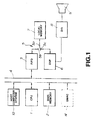
- the speech information processor includes a central processing unit (CPU) 1, as first execution means, a main memory 2, in which control programs etc., for the CPU 1 are stored, and a first-in-first-out (FIFO) 3, as second memory means, which are interconnected via a bus line 4.
- CPU central processing unit
- main memory 2 in which control programs etc., for the CPU 1 are stored
- FIFO first-in-first-out
- the FIFO 3 is connected to a fixed terminal 5b of a changeover switch 5, another fixed terminal 5c of which is connected to a sound source data input terminal of a digital signal processor (DSP) 6.
- the movable contact 5a of the changeover switch 5 is connected to a local memory 7 as first memory means.
- the DSP 6 has its sound source data output terminal connected to an input terminal of a D/A converter 8, an output terminal of which is connected to a speaker unit 9.
- a host computer 10 such as a television game device, having a sound source ROM having sound source data pre-stored therein.
- 16-bit sound source data of various musical instruments such as piano, saxophone or cymbals
- the sound source data having a non-interval portion such as a formant portion FR shown in Fig.9, as in the case of the sound source data of a piano, are stored divided into a non-interval portion and an interval portion (a repetitive portion LP shown in Fig.9).
- the local memory 7 has a storage capacity of, for example, 64 kbytes, with a memory access time being 330 nsec for each memory access operation.
- the programs for the CPU 1 are stored in the local memory 7 in addition to the sound source data.
- the local memory 7 is time-divisionally employed by the CPU 1 and the DSP 6, as will be explained subsequently.
- the above-described speech information processor of the present embodiment operates as follows:
- the CPU 1 causes the sound source data and the control programs to be read out from the sound source ROM of the host computer system 10 and routes the control program over the bus line 4 to the main memory 2, while routing portions of the control program and the sound source data over the bus line 4 to the FIFO 3.
- This stores the control program in the main memory 2, while transiently storing part of the control program and the sound source data in the FIFO 3.
- the DSP 6 controls the changeover switch 5 so that the movable contact 5a is set to the side of the fixed terminal 5c.
- the DSP 6 causes the movable contact 5a of the changeover switch 5 to be set to the side of a fixed terminal 5b if the DSP 6 is not accessing the local memory 7.
- the DSP 6 also has access to the FIFO 3.
- the sound source data temporarily stored in the FIFO 3 is read out sequentially in the order it is stored in the FIFO so as to be routed to and stored in the local memory 7.
- the DSP 6 changes over the switch 5 so that the movable contact 5a is set to the side of the fixed terminal 5c during the execution cycle of the DSP 6 in order to have access to the local memory 7. This transmits the sound source data recorded in the local memory 7 to the DSP 6 via the changeover switch 5.
- data transfer between the CPU 1 and the FIFO 3 can be performed at the transfer rate of the CPU 1.
- the CPU 1 having a high sound source data transfer rate may be employed to assure high-speed data transfer.
- the CPU 1 controls the DSP 6 to cause the sound source data stored in the local memory 7 to be read out if it is desired to process the sound source data stored in the local memory 7.
- the DSP 6 changes over the changeover switch 5 so that the movable contact 5a is set to the side of the fixed terminal 5b.
- the sound source data is read out from the local memory 7 and routed to the FIFO 3. That is, data transfer between the local memory 7 and the FIFO 3 can be performed at the transfer rate proper to the DSP 6.
- the CPU 1 causes sound source data to be read out from the FIFO 3 and processes the read-out data in a pre-set manner during the time the DSP 6 is not accessing the sound source ROM. That is, data transfer between the FIFO 3 and the CPU 1 can be performed at the transfer rate proper to the CPU 1. This enables data transfer rate from the local memory 7 to the CPU 1 to be elevated. Consequently, a vacant area can be provided in the local memory 7 and can be employed for data storage (RAM disc) for e.g. a host computer.
- RAM disc data storage
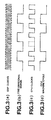
- Memory accessing by the CPU 1 and the DSP 6 is controlled by a synchronization circuit shown for example in Fig.2.
- frequency signals from an oscillator 71 connected to a quartz oscillator 71a are supplied to a first frequency divider 72 and a second frequency divider 73.
- the frequency divider 72 divides the frequency signals in a pre-set manner to produce DSP clocks shown in Fig.3a. These DSP clocks are supplied to clock input terminals of a time-multiplexing control circuit 74 and the DSP 6.
- the time-multiplexing control circuit 74 generates time-divisional signals which go high and low alternately and repeatedly at an interval of four periods of the DSP clocks, with the eight periods of the DSP signals corresponding to one period of the time-divisional signals. These time-divisional signals are fed to first to third switches 77 to 79 and to a comparator 75.
- the second frequency divider 73 has its frequency dividing ratio set to four times that of the first frequency divider 72. By dividing the frequency signal from the oscillator 71 with this frequency dividing ratio, CPU clocks having the frequency equal to one-fourth the frequency of the DSP clocks outputted from the first frequency divider 72, as shown in Fig.3C, are generated, and routes via an AND gate 76 to the CPU 1.
- the CPU 1 Based upon the CPU clocks, the CPU 1 generates machine cycle signals changed in synchronization with the time-multiplexed signals shown in Fig.3b, as shown in Fig.3d, and routes the machine cycle signals to the comparator 75.
- the comparator 75 compares the phase of the time-multiplexed control signal from the time-divisional signal from the time multiplexing control circuit 74 and the machine cycle signal from the CPU 1. If the two signals are in phase with each other, a high-level coincidence detection signal is fed to the AND gate 76. If otherwise, a low-level coincidence detection signal is supplied to the AND gate 76. When fed with the high-level coincidence detection signal, the AND gate routes a CPU clock from the second frequency divider 73 to the clock input terminal of the CPU 1. However, when fed with the low-level coincidence detection signal, the AND gate gates the clock from the second frequency divider 73.
- the CPU clock which should be fed to the CPU 1 is gated by the AND gate 76 and ceases to be supplied to the CPU 1, such that the machine cycle of the CPU 1 is shifted a half cycle to assume a normal state.
- the synchronization circuit controls the memory accessing so that memory accessing by the CPU 1 occurs once for two memory accessing operations performed by the DSP 6.
- the accessing time of the local memory 7 is about 330 nsec, that of the DSP is about 240 nsec, each machine cycle of the CPU 1 ia about 1 ⁇ sc and the memory access time of the CPU 1 is about 375 nsec within the machine cycle of the CPU 1.
- the memory accessing time period Mc of the CPU 1 is set in the latter half of each machine cycle S, as shown in Fig.4d, while two memory accessing time periods MD1, MD2 of the DSP 6 are set in the former half of the machine cycle S, as shown in Fig.4e.
- the accessing time of the local memory 7 is about 330 nsec, so that three accesses MD1, MD2 and MC are set at an equal interval in each machine cycle S, as shown in Fig.4g.
- the time-multiplexing control circuit 74 generates changeover control signals shown in Fig.4f, based on the time-multiplexed signal shown in Fig.4c, and routes the time-multiplexed control signal to the first to third switches 77 to 79.
- the first to third switches 77 to 79 are changed over to select the fixed terminals 77a to 79a by movable contacts 77c to 79c during the periods of the first access MD1 and the second access MD2 of the local memory 7, while being changed over to select the fixed terminals 77b to 79b by the movable contacts 77c to 79c during the period of the third access MC, as shown in Fig.4g.
- the sound source data of the address bus line, data bus line and the control bus line of the local memory 7 are fetched in the DSP 6 during the first access period MD1 and the second access period MD2 of the DSP 6.
- the sound source data of the address bus line, data bus line and the control bus line stored in the FIFO 3 are routed to the local memory 7 during the access period MC of the CPU 1.
- the local memory 7 is employed time-divisionally in common by the DSP 6 and the CPU 1. This improves the exploitation efficiency of the local memory 7 and enables the local memory 7 of a smaller storage capacity to be produced inexpensively, thereby lowering the production cost.
- the local memory 7 stores the sound source data under the numbers of, for example, 0 to 255.
- the sound source data having a non-interval portion (formant portion shown in Fig.9) is stored under numbers different from those for the interval portion (repetitive portion shown in Fig.9).
- the sound source data is read out by eight sound source selection data SRCa to SRCh from the DSP 6.
- the sound source data read out by the eight sound source selection data SRCa to SRCh are routed to signal processors 20A to 20H shown in Fig.5.
- the non-interval portion of the sound source data is routed to the signal processor 20A, while the interval portions of the sound source data are routed to the signal processors 20B to 20H.
- the DSP 6 executes the above processing by software program control. This is explained for convenience by referring to the functional block diagrams shown in Figs.5 and 6.
- the DSP 6 processes the eight sound source data (voice data) A to H time-divisionally for forming and outputting two channels (left and right channels).
- the sampling frequency of the DSP 6 is set to 44.1 Khz, such that a sum total of 128 cycles of the processing operations, with each cycle being 170 nsec, is performed for eight sound source data and two channels within each sampling period (1/ fs).
- the sound source data fed to the signal processors 20A to 20H are supplied to switches SIa to SIh.
- Each of the switches Sia to Sih is red from a register RAM in the DSP 6 with control data KON designating the start (key-on) of sound production of each sound source data, or with control data KOF designating the cessation (key-off) of sound production of each sound source data, via terminals 31a to 31h, so as to be thereby turned on and off.
- Each of the control data is made up of eight bits of data D0 to D7, these data D0 to D7 being associated with key-on and key-off of the sound source data A to H. These control data are written in separate registers.
- the sound source data via the switches Sia to Sih are fed to a data expansion circuit 21 provided in each of the signal processors 20A to 20H. Since the sound source data are compressed from 16 bits to 4 bits and stored in this form in the sound source RAM, the data expansion circuit 21 expands the sound source data compressed to 4 bits to generate 16-bit sound source data which is supplied via a buffer RAM 22 to a pitch conversion circuit 23.
- the pitch conversion circuit 23 is fed with pitch control data P(H) and P(L), such as processing parameters, from the register RAM via a terminal 33a and a control circuit 24.
- pitch control data P(H) and P(L) such as processing parameters
- the pitch conversion circuit 23 interpolates forward side four samples and rear side four samples by over-sampling based upon the pitch control data P(H) and P(L) in order to perform pitch conversion with the same sampling frequency fs as that for the input sound source data.
- the switch S2a is adapted for being turned on and off by the control data FMON (FM-on) supplied from the register RAM via a terminal 35a.
- control data FMON FM-on
- sound source data such as the sound source data H is fed to the control circuit 24.
- the control circuit 24 substitutes the sound source data for the pitch control data P(H) and P(L) in order to transmit the sound source data to the pitch conversion circuit 23.
- the sound source data A is frequency-modulated in the pitch conversion circuit 23, such that, if the modulating signal is of an extremely low frequency of several Hz, vibrato is applied to the modulated signal, whereas, if the modulating signal is of a variable frequency, the sound tone of the playback sound of the modulated signal may be variegated, so that it becomes unnecessary to provide a special sound source for modulation and the FM sound source can be produced by the sampler system.
- the control data FMON is written in an eight-bit register, as is the control data KON, such that the data D0 to D7 of respective bits correspond to the sound source data A to H, respectively.
- the sound source data via the pitch conversion circuit 23 are supplied to a multiplier 26.
- the multiplier is also fed via a terminal 36a, a control circuit 27 and a switch S3a with a control data ENV for controlling the envelope from the register RAM, while being also fed via a terminal 37a, a control circuit 28 and a switch S3a with a control data ADSR for ADSR control.
- the switch S3a is changed over by the upper most bit (MSB) of the control data ADSR, such that, if the MSB of the control data ADSR is "1", the switch S3a is changed over to select the control data ADSR from the control circuit 28 (ADSR mode) and, if the MSB of the control data ADSR is "0", the switch S3a is changed over to select the control data ENV from the control circuit 28 (ENV mode).
- MSB upper most bit
- the multiplier 26 When fed with the control data ENV, the multiplier 26 processes sound source data from the pitch conversion circuit 23 with envelope control such as fading.
- envelope control such as fading.
- envelope control one of five modes, that is direct designation, linear fade-in, kinked line fade-in, linear fade-out and exponential fade-out, may be selected by the upper three bits of the control data ENV.
- the current wave crest value is adopted as the initial value of each mode.
- the multiplier 26 when fed with the control data ADSR, performs a control operation of correspondingly changing the level of the sound source data of each voice on the sound source data from the pitch conversion circuit 23.
- the signal level is raised linearly only during the attack domain, while it is lowered exponentially during the three domains of decay, sustain and release.
- the time duration of the fade-in and fade-out is suitably set for each mode depending on parameter values specified by upper five bits of the control data ENV.
- the time duration of the attack and sustain is suitably set depending on parameter values specified by upper and lower four bits of the control data ADSR, while the sustain level and the time duration of the decay and release is set depending on parameter values specified by each two bits of the control data ADSR.
- the signal level is raised linearly only for the attack period during the ADSR mode for decreasing the number of times of the arithmetic-logical operations.
- the noise data from an M-series noise generator is supplied to the multiplier 26 in lieu of the sound source data from the pitch converter 23.
- the sound source data from the multiplier 26 is fed to second and third multipliers 29l, 29r.
- the second multiplier 29l is fed with left sound volume control data LVL for controlling the left channel sound volume from the register RAM via a terminal 38a
- the third multiplier 29r is fed with right sound volume control data RVL for controlling the right channel sound volume from the register RAM via a terminal 39a.
- the second multiplier 29l multiplies the sound source data with the left sound volume control data LVL for producing left channel sound source data having a pre-set sound volume and outputting the produced data via a terminal TLa.
- the third multiplier 29r multiplies the sound source data with the right sound volume control data RVL for producing right channel sound source data having a pre-set sound volume and outputting the produced data via a terminal TRa.
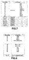
- Figs.7 and 8 show maps for all of the control data on the register RAM.
- left channel sound source data generated by the signal processing units 20A to 20H, are supplied via terminals Tla to TLh shown in Fig.6 to a left channel signal processing unit 50L, while the right channel sound source data are supplied via terminals Tra to TRh to a right channel signal processing unit 50L.
- the sound source data supplied via the terminals Tla to Tlh are fed to a main additive unit 51ml, while being fed via switches S4a to S4h to a subsidiary additive unit 51el.
- the sound source data supplied via the terminals Tra to Trh are fed to a main additive unit 51mr, while being fed via switches S5a to S5h to a subsidiary additive unit 51er.
- the additive units 51ml, 51mr add the sound source data supplied thereto via the terminals TL a to Tlh and Tra to Trh to supply the resulting sums to a multiplier 52.
- the multiplier 52 is fed from the register RAM via a terminal 62 with control data MVL for controlling the main sound volume.
- the multiplier 52 multiplies the sound source data with the control data MVL to control the main sound volume of the sound source data and transmits the resulting product to an additive unit 53.
- control data EONa to EONh for adding the echo (reverberating sound) from the register RAM via terminals 61a to 61h.
- the sound source data (voice) to be added to with the echo is selected by these control data EONa to EONh.
- the switches S4a and S5a are controlled so as to be turned off so that no echo is added to the non-interval portion.
- control data EON is written in an 8-bit register, as shown in Fig.8.
- the subsidiary additive nodes 51el, 51er add the sound source data supplied via the switches S4a to S4h and S5a to S5h and transmit the resulting sum data to channel echo control units 14El, 14Rr via an additive unit 54.
- the echo control units 14El, 14Er are fed via a terminal 64 with control data EDL (echo delay) for controlling the amount of the echo and control data ESA (echo start address) indicating the sound source data to be added to with echo.
- the echo control units 14EL, 14Er add echo to the sound source data from the subsidiary additive units 51el, 51er within the range of 255 msec so that the left channel echo and the right channel echo will be equal to each other, and transmits the resulting data via a buffer RAM 55 to a digital low-pass filter, such as a finite impulse response (FIR) filter 56.
- a digital low-pass filter such as a finite impulse response (FIR) filter 56.
- FIR finite impulse response
- the FIR filter 56 is fed from the register RAM via a terminal 66 with 8-bit coefficients C0 to C7, added to with codes, and has its filter characteristics variably controlled so that the echo sound will be produced which is spontaneous in psychoacoustic effects.
- the sound source data via the FIR filter 56 is supplied to multipliers 57, 58.
- the multiplier 57 is supplied with control data EFB (echo feedback) from the register RAM via a terminal 57.
- the multiplier 57 multiplies the sound source data from the FIR filter 56 with the control data EFB and routes the resulting product to the additive unit 54.
- the additive unit 54 adds the sound source data from the subsidiary additive units 51el and 51Er to the sound source data from the multiplier 57z and routes the resulting sum to the echo control units 14El and 14Er.
- the multiplier 58 is fed with the control data EVL for controlling the amount of the echo sound from the register RAM via a terminal 68.
- the multiplier 58 multiplies the sound source from the FIR filter 56 by the control data EVL to adjust the sound volume of the echo in the sound source data and routes the resulting product to the additive unit 53.
- the additive unit 53 sums the sound source data from the main additive units 51ml and 51mr to the sound source data from the multiplier 58 to add the echo to the sound source data from the multiplier 51mr, and outputs the resulting sum via an over-sampling filter 59 and a left-channel sound source data output terminal Lout and a right-channel sound source terminal Rout, respectively.
- the sound source data outputted from the DSP 6 via output terminals Lout, Rout are fed to the D/A converter 8 shown in Fig.1.
- the D/A converter 8 converts the sound source data into analog signals to form speech signals which are supplied to the speaker unit 9.
- the speech corresponding to the sound source data is produced by the speaker unit 9.
- the control data MVL for controlling the main sound volume and the control data for controlling the echo sound volume are 8-bit data devoid of codes and are independent of each other and with respect to the left and right channels.
- the main speech signal and the echo signal may be adjusted in level independently of each other to render the speech produced by the speaker unit 9 sufficient in ambience.
- a direct memory access controller (DMAC) 11 may also be provided as shown by a broken line in Fig.1 for transferring the sound source data read out from the sound source ROM to the FIFO 3.
- the DMAC is a hardware designed for use exclusively for data transfer, the sound source data may be transferred without the interposition of the CPU 1, so that faster data transfer may be achieved than is possible with the CPU 1.
- the local memory 7 has a storage capacity of 64 kbytes, and the memory access time is 330 nsec.
- these numerical values are merely illustrative and are not limitative of the present invention.
- the present invention is not limited to the numerical values given herein and may be modified in a desired manner without departing from the scope of the invention.
Description
- This invention relates to a speech information processor which may, for example, advantageously be employed in an electronic musical instrument or a television game device.
- The sound sources employed in general in an electronic musical instrument or a television game may be roughly classified into analog sound sources, comprising a voltage-controlled oscillator (VCO), a voltage-controlled amplifier (VCA), a voltage-controlled filter (VCF) etc., and digital sound sources, such as a programmable sound generator (PSG) or a zigzag readout type ROM.
- As an example of a digital sound source, Japanese Patent Applications Publications No. JP-A-62264099 (1987) or JP-A-62267798 (1987) disclose a sampler sound source in which sound source data sampled from live instrument sound and digitally processed is stored in a memory for use as a sound source.
- The above-mentioned sound source (sampler sound source) stores only sound source data of a pre-set pitch (interval) after compression by, for example, non-linear quantization. Each sound source data is stored in two parts, that is in a formant portion (FR) and a one-period portion (LP) of plural repeated waveforms of the fundamental period following the formant portion, as shown in Fig.4. The formant portion is a signal waveform at the initial stage of sound production proper to each musical instrument, such as a sound produced from when a key of a keyboard is struck until a hammer hits the string in the case of a piano. During readout of the sound source data, the formant portion is read out first and the one-period portion is read out a plurality of times.
- Since the above sound source data is compressed, and only the required portions, that is the above formant portion and the one-cycle repetitive portion, are extracted and stored, a large quantity of sound source data may be stored in a smaller storage space.
- As a general speech information processor for data processing of the sampler sound source, an audio processing unit (APU) 107 consisting of a digital signal processing unit (DSP) 101, a
memory 102 and a central processing unit (CPU) 103, as shown in Fig.10, has been proposed. - In this figure, the APU 107 is connected to a
host computer 104, provided in a customary personal computer, a digital electronic musical instrument or a TV game machine. - The
host computer 104 includes a ROM cassette storing the above-mentioned sound source data, control programs, etc. The control program stored in the ROM cassette is read out by theCPU 103 so as to be stored in a working memory (RAM) 103a therein. - The
CPU 103 causes the sound source data to be read out from the ROM cassette and transiently stored in thememory 102 via the DSP 101, based upon the above-mentioned control program by way of performing writing control for thememory 102. TheCPU 103 also controls the DSP 101 in accordance with the control program. The DSP 101 causes the sound source data stored in thememory 102 to be read out under control by theCPU 103 and processes the sound source data thus read out with, for example, bit expansion or pitch conversion. The DSP 101 also processes the sound source data with looping for reading out the repetitive portion of the sound source data a plurality of number of times. The sound source data, outputted by the DSP 101 after such processing operations, is fed by a D/A converter 105 and thereby converted into analog speech signals which are fed to aspeaker unit 106. Thus an acoustic output corresponding to the speech sound data can be produced via thespeaker unit 106. - The access timing to the
memory 102 by theCPU 103 and the DSP 101 is pre-set so that theCPU 101 accesses thememory 102 once after theDSP 101 accesses the memory twice. Consequently, when partially rewriting the sound source data of thememory 102, theCPU 103 controls the writing in thememory 102 so that the CPU reads out sound source data from the ROM cassette and writes the data in thememory 102 during the time theDSP 101 is not accessing the memory. This enables the acoustic output corresponding to the rewritten scund source data to be produced from the next time on. The present applicants have filed a related European Application Publication No. EP-A-0 543 667 and corresponding US Patent Nos. US-A-5 390 158 and US-A-5 539 716. - However, with the above speech information processor employing the
APU 107, thememory 102 is used in common by the DSP 101 and theCPU 103, and the access timing of theDSP 101 and theCPU 103 to thememory 102 is pre-set, such that the it is possible for theCPU 103 to have access to the memory only at the pre-set timing and hence high-speed data transfer cannot be achieved. - Conversely, the high-speed CPU cannot be employed because high speed data transfer cannot be achieved.
- If memory access is had by interrupt, for example, for achieving high-speed data transfer, when speech data is being read out by the DSP 101, speech data readout is necessarily interrupted, such that speech data outputting cannot be made continuously.
- EP-A-0 421 696 discloses a staggered access memory system in which a number of memory access devices (such as processors or intelligent controllers) operate via a memory interface device to provide time-division access to one or more memory units. The phase relationship between the time-division access opportunities of each memory unit is controlled, so that one or more access devices can address the respective memory units simultaneously.
- GB-A-2 263 047 discloses an interface chip for a voice processing system. Requests can be received from two processors and the flow of data therebetween can be controlled. The interface chip acts as a dual port controller for interaction of RAMs and processors of the voice processing system.
- The present invention provides apparatus for processing speech information, comprising
- first execution means and second execution means for executing operations at respective different execution cycles, and
- first memory means for reading and recording the speech information,
- said first execution means and said second execution means both exploiting said first memory means in time division manner for processing the speech information,
- said apparatus further comprising
- second memory means for transiently storing transferred speech information between said first execution means and said first memory means,
- said first execution means recording the speech information on or reading the speech information from said second memory means during the execution cycle of said first execution means,
- said second execution means accessing said first memory means during the execution cycle of said second execution means for outputting the speech information,
- the speech information recorded in said second memory means being read out therefrom and recorded in said first memory means, or the speech information recorded in said first memory means being read out therefrom and recorded in said second memory means during the time that said second execution means is not accessing said first memory means.
-
- The apparatus preferably further comprises a direct memory access controller for recording the speech information on or reproducing the speech information from the second memory means.
- In view of the problems explained above, a preferred embodiment of the invention described hereinbelow provides a speech information processor in which, even if memory is exploited in common by a CPU and a DSP, and the memory access timing is pre-set, high-speed data transfer may be achieved without interrupting the DSP operations.
- With the speech information processing apparatus according to the preferred embodiment of the invention, the execution cycles of the first execution means, for example a central processing unit (CPU), and the second execution means, for example a digital signal processor (DSP), are pre-set so that two execution cycles of the DSP are carried out for each execution cycle of the CPU, and the first memory means for recording and readout of the speech information is alternately used by the CPU and the DSP by these different execution cycles for processing the speech information.
- The first memory means is preceded by second memory means via which the speech information is written into and read out from the first memory means.
- Specifically, the CPU, reading out the speech information from the sound source ROM of, for example, a TV game device, controls the writing in the second storage means for causing the speech information to be stored therein transiently. That is, the recording of the speech information in the second memory means is carried out during the execution cycle of the CPU.
- If more than a pre-set quantity of the speech information is stored in the storage area of the second memory means, the DSP reads out the speech information stored in the second memory means during the time the DSP is not accessing the first memory means, such as during the execution cycle of the CPU, and controls the writing in the first memory means so that the speech information thus read out will be stored in the first memory means. That is, the recording of the speech information in the first memory means is carried out during the execution cycle of the DSP.
- During its execution cycle, the DSP reads out the speech information stored in the first memory means and processes the speech information thus read out with, for example, bit expansion or pitch conversion. An output of the DSP, which is the speech information processed with bit expansion etc., is routed to a speaker device or the like. The speaker device produces an acoustic output corresponding to the speech information.
- When reading out the speech information stored in the first memory means, the CPU demands the DSP to read out the speech information stored in the first memory means. This causes the speech information to be read out from the first memory means during the execution cycle of the DSP so as to be recorded in the second memory means. That is, the writing of the speech information in the second memory means in such case is carried out at the DSP timing.
- When the speech information has been recorded in the second memory means, the CPU causes the speech information to be read out from the second memory means. That is, the writing of the speech information in the second memory means in such case is earried out at the CPU timing.
- Even although the execution cycles of the CPU and the DSP are pre-set, and the first memory means is co-used by the CPU and the DSP, transfer of the speech information between the CPU and the second memory means is carried out at the CPU timing by the operation of the second memory means, so that high-speed transfer becomes possible through the use of the CPU having the high transfer rate of the speech information.
- On the other hand, since the transfer of the speech information between the second memory means and the first memory means is carried out at the DSP timing during the time the DSP is not accessing the first memory means, it becomes possible to transfer the speech information without interrupting the information processing by the DSP, so that continuous outputting of the speech information may be prevented from being interrupted.
- The apparatus for processing speech information embodying the present invention includes a direct accessing controller (DMAC) in the second memory means for recording and readout of the speech information.
- If the speech inrormation is to be transferred, the DMAC routes a bus request signal to the CPU in order to obtain a permission of using the bus line. When fed with the bus request signal, the CPU interrupts the operation it is performing at an opportune point and routes an acknowledge signal permitting the use of the bus line to the DMC. When fed with the bus acknowledge signal, the DMC transfers the speech information read out from the CPU to the second memory means, or reads out the speech information stored in the second memory means in order to route the read-out speech information to the CPU.
- In distinction from the CPU, performing the transfer of the speech information in accordance with the control program, the DMAC is a hardware designed for exclusive use in information transfer and hence is capable of faster information transfer than is possible with the CPU.
- In sum, with the apparatus for processing speech information embodying the present invention, since the transfer of the speech information between the first execution means and the second execution means may be performed at the timing of the first execution means, the first execution means having a high rate of transfer of the speech information may be employed, thus rendering it possible to achieve high speed transfer.
- On the other hand, since the transfer of the speech information between the second memory means and the first memory means is performed at the timing of the second execution means during the time the second execution means is not accessing the first memory means, the transfer of the speech information may be achieved without interrupting the information processing by the second execution means, so that the continuous outputting of the speech information may be prevented from being interrupted.
- In addition, with the apparatus for processing speech information embodying the present invention, by employing the direct memory access controller (DMAC), the information transfer becomes possible without the interposition of the CPU, thereby making possible faster information transfer than is possible with the CPU.
- Furthermore, since it is possible to perform high speed transfer of the speech information, high-speed transfer of the speech information becomes possible between the first execution means and the first memory means, so that a vacant area can be formed in the first storage means. Such vacant area in the first memory means may be exploited as data storage for a host computer (RAM disc).
- The invention will now be further described, by way of illustrative and non-limiting example, in the form of a detailed description of the preferred embodiment described in outline above, the description making reference to the accompanying drawings, in which:
- Fig.1 is a block diagram showing the speech information processor according to the preferred embodiment of the invention.
- Fig.2 is a block diagram of a synchronization circuit for controlling a CPU and a DSP provided in the speech information processor of Fig.1 so as to exploit local memory time-divisionally.
- Fig.3 is a timing chart for illustrating the operation of the synchronization circuit.
- Fig.4 is a timing chart for illustrating the operation of the synchronization circuit.
- Fig.5 is a block diagram showing a portion of the DSP provided in the speech information processor embodying the present invention.
- Fig.6 is a block diagram showing another portion of the DSP provided in the speech information processor embodying the present invention.
- Fig.7 illustrates a map of control data on a register RAM provided in the DSP.
- Fig.8 illustrates a map of control data on a register RAM provided in the DSP.
- Fig.9 illustrates sound source data of a non-interval portion and an interval portion separately stored in a sampler sound source.
- Fig.10 is block view showing a previously proposed speech information processor.
-
- Referring to the drawings, a preferred embodiment of a speech information processor according to the present invention will be explained.
- The speech information processor includes a central processing unit (CPU) 1, as first execution means, a
main memory 2, in which control programs etc., for theCPU 1 are stored, and a first-in-first-out (FIFO) 3, as second memory means, which are interconnected via a bus line 4. - The
FIFO 3 is connected to a fixed terminal 5b of achangeover switch 5, another fixedterminal 5c of which is connected to a sound source data input terminal of a digital signal processor (DSP) 6. Themovable contact 5a of thechangeover switch 5 is connected to alocal memory 7 as first memory means. TheDSP 6 has its sound source data output terminal connected to an input terminal of a D/A converter 8, an output terminal of which is connected to aspeaker unit 9. - To the bus line 4 is connected a
host computer 10, such as a television game device, having a sound source ROM having sound source data pre-stored therein. - In the sound source ROM of the
host computer 10, 16-bit sound source data of various musical instruments, such as piano, saxophone or cymbals, are stored in a 4-bit compressed form. The sound source data having a non-interval portion, such as a formant portion FR shown in Fig.9, as in the case of the sound source data of a piano, are stored divided into a non-interval portion and an interval portion (a repetitive portion LP shown in Fig.9). - The
local memory 7 has a storage capacity of, for example, 64 kbytes, with a memory access time being 330 nsec for each memory access operation. The programs for theCPU 1 are stored in thelocal memory 7 in addition to the sound source data. Thelocal memory 7 is time-divisionally employed by theCPU 1 and theDSP 6, as will be explained subsequently. - The above-described speech information processor of the present embodiment operates as follows:
- When the game is started, the
CPU 1 causes the sound source data and the control programs to be read out from the sound source ROM of thehost computer system 10 and routes the control program over the bus line 4 to themain memory 2, while routing portions of the control program and the sound source data over the bus line 4 to theFIFO 3. This stores the control program in themain memory 2, while transiently storing part of the control program and the sound source data in theFIFO 3. - Until the sound source data is stored in more than a pre-set amount in the
FIFO 3, theDSP 6 controls thechangeover switch 5 so that themovable contact 5a is set to the side of the fixedterminal 5c. When more than a pre-set amount of the sound source data is stored in theFIFO 3, theDSP 6 causes themovable contact 5a of thechangeover switch 5 to be set to the side of a fixed terminal 5b if theDSP 6 is not accessing thelocal memory 7. TheDSP 6 also has access to theFIFO 3. Thus the sound source data temporarily stored in theFIFO 3 is read out sequentially in the order it is stored in the FIFO so as to be routed to and stored in thelocal memory 7. - On the other hand, the
DSP 6 changes over theswitch 5 so that themovable contact 5a is set to the side of the fixed terminal 5c during the execution cycle of theDSP 6 in order to have access to thelocal memory 7. This transmits the sound source data recorded in thelocal memory 7 to theDSP 6 via thechangeover switch 5. - That is, data transfer between the
CPU 1 and theFIFO 3 can be performed at the transfer rate of theCPU 1. Thus theCPU 1 having a high sound source data transfer rate may be employed to assure high-speed data transfer. - On the other hand, data transfer between the
FIFO 3 and thelocal memory 7 and that between thelocal memory 7 and theDSP 6 can be preformed at the transfer rate proper to theDSP 6. Besides, sound source data transfer between theFIFO 3 and thelocal memory 7 is performed during the time theDSP 6 is not accessing thelocal memory 7. Consequently, sound source data may be transferred without interrupting data processing by theDSP 6. Thus it becomes possible to prevent interruption of a continuous speech output. - The
CPU 1 controls theDSP 6 to cause the sound source data stored in thelocal memory 7 to be read out if it is desired to process the sound source data stored in thelocal memory 7. Thus theDSP 6 changes over thechangeover switch 5 so that themovable contact 5a is set to the side of the fixed terminal 5b. Besides, during the time theDSP 6 is not reading out the sound source data stored in thelocal memory 7, the sound source data is read out from thelocal memory 7 and routed to theFIFO 3. That is, data transfer between thelocal memory 7 and theFIFO 3 can be performed at the transfer rate proper to theDSP 6. - If more than a pre-set amount of the sound source data is stored in the
FIFO 3, theCPU 1 causes sound source data to be read out from theFIFO 3 and processes the read-out data in a pre-set manner during the time theDSP 6 is not accessing the sound source ROM. That is, data transfer between theFIFO 3 and theCPU 1 can be performed at the transfer rate proper to theCPU 1. This enables data transfer rate from thelocal memory 7 to theCPU 1 to be elevated. Consequently, a vacant area can be provided in thelocal memory 7 and can be employed for data storage (RAM disc) for e.g. a host computer. - Memory accessing by the
CPU 1 and theDSP 6 is controlled by a synchronization circuit shown for example in Fig.2. - In the synchronization circuit, shown in Fig.2, frequency signals from an
oscillator 71 connected to a quartz oscillator 71a are supplied to afirst frequency divider 72 and a second frequency divider 73. Thefrequency divider 72 divides the frequency signals in a pre-set manner to produce DSP clocks shown in Fig.3a. These DSP clocks are supplied to clock input terminals of a time-multiplexingcontrol circuit 74 and theDSP 6. - The time-multiplexing
control circuit 74 generates time-divisional signals which go high and low alternately and repeatedly at an interval of four periods of the DSP clocks, with the eight periods of the DSP signals corresponding to one period of the time-divisional signals. These time-divisional signals are fed to first tothird switches 77 to 79 and to acomparator 75. - The second frequency divider 73 has its frequency dividing ratio set to four times that of the
first frequency divider 72. By dividing the frequency signal from theoscillator 71 with this frequency dividing ratio, CPU clocks having the frequency equal to one-fourth the frequency of the DSP clocks outputted from thefirst frequency divider 72, as shown in Fig.3C, are generated, and routes via an ANDgate 76 to theCPU 1. - Based upon the CPU clocks, the
CPU 1 generates machine cycle signals changed in synchronization with the time-multiplexed signals shown in Fig.3b, as shown in Fig.3d, and routes the machine cycle signals to thecomparator 75. - The
comparator 75 compares the phase of the time-multiplexed control signal from the time-divisional signal from the time multiplexingcontrol circuit 74 and the machine cycle signal from theCPU 1. If the two signals are in phase with each other, a high-level coincidence detection signal is fed to the ANDgate 76. If otherwise, a low-level coincidence detection signal is supplied to the ANDgate 76. When fed with the high-level coincidence detection signal, the AND gate routes a CPU clock from the second frequency divider 73 to the clock input terminal of theCPU 1. However, when fed with the low-level coincidence detection signal, the AND gate gates the clock from the second frequency divider 73. - Consequently, when the two signals are not in phase with each other, the CPU clock which should be fed to the
CPU 1 is gated by the ANDgate 76 and ceases to be supplied to theCPU 1, such that the machine cycle of theCPU 1 is shifted a half cycle to assume a normal state. - Thus the synchronization circuit controls the memory accessing so that memory accessing by the
CPU 1 occurs once for two memory accessing operations performed by theDSP 6. - Specifically, the accessing time of the
local memory 7 is about 330 nsec, that of the DSP is about 240 nsec, each machine cycle of theCPU 1 ia about 1 µsc and the memory access time of theCPU 1 is about 375 nsec within the machine cycle of theCPU 1. - Assuming that the DSP clocks supplied to the
DSP 6 by the synchronization circuit, the CPU clocks supplied to theCPU 1 and the time-multiplexed signal outputted from the time-multiplexingcontrol circuit 74 are produced under a regular condition as shown in Figs.4a to 4c, the memory accessing time period Mc of theCPU 1 is set in the latter half of each machine cycle S, as shown in Fig.4d, while two memory accessing time periods MD1, MD2 of theDSP 6 are set in the former half of the machine cycle S, as shown in Fig.4e. - On the other hand, the accessing time of the
local memory 7 is about 330 nsec, so that three accesses MD1, MD2 and MC are set at an equal interval in each machine cycle S, as shown in Fig.4g. - Thus an offset is produced in the accessing time of the
local memory 7,DSP 6 and theCPU 1. Such offset in the accessing time is adjusted by switching control of the first tothird switches 77 to 79 by the time-multiplexingcontrol circuit 74 shown in Fig.2 and sound source data writing and readout via theFIFO 3. - That is, the time-multiplexing
control circuit 74 generates changeover control signals shown in Fig.4f, based on the time-multiplexed signal shown in Fig.4c, and routes the time-multiplexed control signal to the first tothird switches 77 to 79. Thus the first tothird switches 77 to 79 are changed over to select the fixedterminals 77a to 79a bymovable contacts 77c to 79c during the periods of the first access MD1 and the second access MD2 of thelocal memory 7, while being changed over to select the fixedterminals 77b to 79b by themovable contacts 77c to 79c during the period of the third access MC, as shown in Fig.4g. - Thus the sound source data of the address bus line, data bus line and the control bus line of the
local memory 7 are fetched in theDSP 6 during the first access period MD1 and the second access period MD2 of theDSP 6. - On the other hand, the sound source data of the address bus line, data bus line and the control bus line stored in the
FIFO 3 are routed to thelocal memory 7 during the access period MC of theCPU 1. - Thus, with the speech information processor of the present embodiment, the
local memory 7 is employed time-divisionally in common by theDSP 6 and theCPU 1. This improves the exploitation efficiency of thelocal memory 7 and enables thelocal memory 7 of a smaller storage capacity to be produced inexpensively, thereby lowering the production cost. - The
local memory 7 stores the sound source data under the numbers of, for example, 0 to 255. The sound source data having a non-interval portion (formant portion shown in Fig.9) is stored under numbers different from those for the interval portion (repetitive portion shown in Fig.9). The sound source data is read out by eight sound source selection data SRCa to SRCh from theDSP 6. The sound source data read out by the eight sound source selection data SRCa to SRCh are routed to signalprocessors 20A to 20H shown in Fig.5. - If the sound source data, stored in the local memory by being divided into the non-interval portion and the interval portions, are read out, the non-interval portion of the sound source data is routed to the
signal processor 20A, while the interval portions of the sound source data are routed to thesignal processors 20B to 20H. TheDSP 6 executes the above processing by software program control. This is explained for convenience by referring to the functional block diagrams shown in Figs.5 and 6. - The
DSP 6 processes the eight sound source data (voice data) A to H time-divisionally for forming and outputting two channels (left and right channels). Specifically, the sampling frequency of theDSP 6 is set to 44.1 Khz, such that a sum total of 128 cycles of the processing operations, with each cycle being 170 nsec, is performed for eight sound source data and two channels within each sampling period (1/ fs). - That is, the sound source data fed to the
signal processors 20A to 20H are supplied to switches SIa to SIh. Each of the switches Sia to Sih is red from a register RAM in theDSP 6 with control data KON designating the start (key-on) of sound production of each sound source data, or with control data KOF designating the cessation (key-off) of sound production of each sound source data, via terminals 31a to 31h, so as to be thereby turned on and off. - Each of the control data is made up of eight bits of data D0 to D7, these data D0 to D7 being associated with key-on and key-off of the sound source data A to H. These control data are written in separate registers.
- Thus it suffices for the user to set a flag "1" for the sound source data desired to be keyed on or off, so that the laborious operation of preparing a program in which a bit not changed for each sound note is temporarily written in the buffer register may be eliminated.
- The sound source data via the switches Sia to Sih are fed to a
data expansion circuit 21 provided in each of thesignal processors 20A to 20H. Since the sound source data are compressed from 16 bits to 4 bits and stored in this form in the sound source RAM, thedata expansion circuit 21 expands the sound source data compressed to 4 bits to generate 16-bit sound source data which is supplied via abuffer RAM 22 to apitch conversion circuit 23. - The
pitch conversion circuit 23 is fed with pitch control data P(H) and P(L), such as processing parameters, from the register RAM via aterminal 33a and acontrol circuit 24. Thus thepitch conversion circuit 23 interpolates forward side four samples and rear side four samples by over-sampling based upon the pitch control data P(H) and P(L) in order to perform pitch conversion with the same sampling frequency fs as that for the input sound source data. - If lower bits of the control data P(L) are set to 0, it becomes possible to prevent the interpolating data from being non-uniformly thinned out and hence to prevent fine pitch wobbling in order to produce the high-quality playback sound.
- The switch S2a is adapted for being turned on and off by the control data FMON (FM-on) supplied from the register RAM via a terminal 35a. When the switch 2a is turned on by the control data FMON, sound source data such as the sound source data H is fed to the
control circuit 24. When fed with such other sound source data, thecontrol circuit 24 substitutes the sound source data for the pitch control data P(H) and P(L) in order to transmit the sound source data to thepitch conversion circuit 23. - Thus the sound source data A is frequency-modulated in the
pitch conversion circuit 23, such that, if the modulating signal is of an extremely low frequency of several Hz, vibrato is applied to the modulated signal, whereas, if the modulating signal is of a variable frequency, the sound tone of the playback sound of the modulated signal may be variegated, so that it becomes unnecessary to provide a special sound source for modulation and the FM sound source can be produced by the sampler system. - The control data FMON is written in an eight-bit register, as is the control data KON, such that the data D0 to D7 of respective bits correspond to the sound source data A to H, respectively.
- The sound source data via the
pitch conversion circuit 23 are supplied to amultiplier 26. The multiplier is also fed via aterminal 36a, acontrol circuit 27 and a switch S3a with a control data ENV for controlling the envelope from the register RAM, while being also fed via aterminal 37a, acontrol circuit 28 and a switch S3a with a control data ADSR for ADSR control. - The switch S3a is changed over by the upper most bit (MSB) of the control data ADSR, such that, if the MSB of the control data ADSR is "1", the switch S3a is changed over to select the control data ADSR from the control circuit 28 (ADSR mode) and, if the MSB of the control data ADSR is "0", the switch S3a is changed over to select the control data ENV from the control circuit 28 (ENV mode).
- When fed with the control data ENV, the
multiplier 26 processes sound source data from thepitch conversion circuit 23 with envelope control such as fading. As for such envelope control, one of five modes, that is direct designation, linear fade-in, kinked line fade-in, linear fade-out and exponential fade-out, may be selected by the upper three bits of the control data ENV. The current wave crest value is adopted as the initial value of each mode. - It is noted that, if the sound source is a drum or a piano, the total sound production period is divided into an attack domain, a decay domain, sustain domain and a release domain, and the signal amplitude exhibits peculiar change state in each domain. Thus, when fed with the control data ADSR, the
multiplier 26 performs a control operation of correspondingly changing the level of the sound source data of each voice on the sound source data from thepitch conversion circuit 23. - Specifically, with such control operation, the signal level is raised linearly only during the attack domain, while it is lowered exponentially during the three domains of decay, sustain and release. The time duration of the fade-in and fade-out is suitably set for each mode depending on parameter values specified by upper five bits of the control data ENV.
- The time duration of the attack and sustain is suitably set depending on parameter values specified by upper and lower four bits of the control data ADSR, while the sustain level and the time duration of the decay and release is set depending on parameter values specified by each two bits of the control data ADSR.
- With the
present DSP 6, the signal level is raised linearly only for the attack period during the ADSR mode for decreasing the number of times of the arithmetic-logical operations. By switching the ADSR mode to the ENV mode, setting the attack domain to the kinked line fade-in and setting the three domains of decay, sustain and release to exponential fade-out, it is possible to manually perform spontaneous ADSR control operations. - By supplying output sound source data of the
multiplier 26 via a terminal 41a to the register RAM and supplying the control data ENV via a terminal 42a to the register RAM for rewriting for each sample period, it becomes possible to produce speech signals of arbitrary envelope characteristics having significantly different pitches from the sound source data of the same musical instrument. - If the noise is employed as the effect sound, the noise data from an M-series noise generator, not shown, is supplied to the
multiplier 26 in lieu of the sound source data from thepitch converter 23. - The sound source data from the
multiplier 26 is fed to second andthird multipliers 29l, 29r. The second multiplier 29l is fed with left sound volume control data LVL for controlling the left channel sound volume from the register RAM via a terminal 38a, while thethird multiplier 29r is fed with right sound volume control data RVL for controlling the right channel sound volume from the register RAM via a terminal 39a. - The second multiplier 29l multiplies the sound source data with the left sound volume control data LVL for producing left channel sound source data having a pre-set sound volume and outputting the produced data via a terminal TLa. The
third multiplier 29r multiplies the sound source data with the right sound volume control data RVL for producing right channel sound source data having a pre-set sound volume and outputting the produced data via a terminal TRa. - Figs.7 and 8 show maps for all of the control data on the register RAM.
- Thus the left channel sound source data, generated by the
signal processing units 20A to 20H, are supplied via terminals Tla to TLh shown in Fig.6 to a left channel signal processing unit 50L, while the right channel sound source data are supplied via terminals Tra to TRh to a right channel signal processing unit 50L. - In the left channel signal processing unit 50L, the sound source data supplied via the terminals Tla to Tlh are fed to a main additive unit 51ml, while being fed via switches S4a to S4h to a subsidiary additive unit 51el.
- In the right channel
signal processing unit 50R, the sound source data supplied via the terminals Tra to Trh are fed to a main additive unit 51mr, while being fed via switches S5a to S5h to a subsidiary additive unit 51er. - The additive units 51ml, 51mr add the sound source data supplied thereto via the terminals TL a to Tlh and Tra to Trh to supply the resulting sums to a
multiplier 52. - The
multiplier 52 is fed from the register RAM via a terminal 62 with control data MVL for controlling the main sound volume. Themultiplier 52 multiplies the sound source data with the control data MVL to control the main sound volume of the sound source data and transmits the resulting product to anadditive unit 53. - To the switches S4a to S4h and S5a to S5h of the
signal processors 50L, 50R are routed control data EONa to EONh for adding the echo (reverberating sound) from the register RAM via terminals 61a to 61h. The sound source data (voice) to be added to with the echo is selected by these control data EONa to EONh. - When the signal processing of the non-interval component is performed by the
signal processing unit 20A for the voice A, the switches S4a and S5a are controlled so as to be turned off so that no echo is added to the non-interval portion. - The control data EON is written in an 8-bit register, as shown in Fig.8.
- The subsidiary additive nodes 51el, 51er add the sound source data supplied via the switches S4a to S4h and S5a to S5h and transmit the resulting sum data to channel echo control units 14El, 14Rr via an
additive unit 54. - The echo control units 14El, 14Er are fed via a terminal 64 with control data EDL (echo delay) for controlling the amount of the echo and control data ESA (echo start address) indicating the sound source data to be added to with echo. The echo control units 14EL, 14Er add echo to the sound source data from the subsidiary additive units 51el, 51er within the range of 255 msec so that the left channel echo and the right channel echo will be equal to each other, and transmits the resulting data via a
buffer RAM 55 to a digital low-pass filter, such as a finite impulse response (FIR)filter 56. - The
FIR filter 56 is fed from the register RAM via a terminal 66 with 8-bit coefficients C0 to C7, added to with codes, and has its filter characteristics variably controlled so that the echo sound will be produced which is spontaneous in psychoacoustic effects. The sound source data via theFIR filter 56 is supplied tomultipliers - The
multiplier 57 is supplied with control data EFB (echo feedback) from the register RAM via aterminal 57. Themultiplier 57 multiplies the sound source data from theFIR filter 56 with the control data EFB and routes the resulting product to theadditive unit 54. Theadditive unit 54 adds the sound source data from the subsidiary additive units 51el and 51Er to the sound source data from the multiplier 57z and routes the resulting sum to the echo control units 14El and 14Er. - The
multiplier 58 is fed with the control data EVL for controlling the amount of the echo sound from the register RAM via aterminal 68. Themultiplier 58 multiplies the sound source from theFIR filter 56 by the control data EVL to adjust the sound volume of the echo in the sound source data and routes the resulting product to theadditive unit 53. - The
additive unit 53 sums the sound source data from the main additive units 51ml and 51mr to the sound source data from themultiplier 58 to add the echo to the sound source data from the multiplier 51mr, and outputs the resulting sum via anover-sampling filter 59 and a left-channel sound source data output terminal Lout and a right-channel sound source terminal Rout, respectively. - The sound source data outputted from the
DSP 6 via output terminals Lout, Rout are fed to the D/A converter 8 shown in Fig.1. The D/A converter 8 converts the sound source data into analog signals to form speech signals which are supplied to thespeaker unit 9. Thus the speech corresponding to the sound source data is produced by thespeaker unit 9. - The control data MVL for controlling the main sound volume and the control data for controlling the echo sound volume are 8-bit data devoid of codes and are independent of each other and with respect to the left and right channels. Thus the main speech signal and the echo signal may be adjusted in level independently of each other to render the speech produced by the
speaker unit 9 sufficient in ambience. - In the above description, the sound source data read out from the sound source ROM of the
host computer system 10 is written in theFIFO 3 under control by theCPU 1. However, a direct memory access controller (DMAC) 11 may also be provided as shown by a broken line in Fig.1 for transferring the sound source data read out from the sound source ROM to theFIFO 3. - Since the DMAC is a hardware designed for use exclusively for data transfer, the sound source data may be transferred without the interposition of the
CPU 1, so that faster data transfer may be achieved than is possible with theCPU 1. - In addition, in the above description, the
local memory 7 has a storage capacity of 64 kbytes, and the memory access time is 330 nsec. However, these numerical values are merely illustrative and are not limitative of the present invention. Thus the present invention is not limited to the numerical values given herein and may be modified in a desired manner without departing from the scope of the invention.
Claims (10)
- Apparatus for processing speech information, comprisingfirst execution means (1) and second execution means (6) for executing operations at respective different execution cycles, andfirst memory means (7) for reading and recording the speech information,said first execution means (1) and the second execution means (6) both exploiting said first memory means (7) in time division manner for processing the speech information,
said apparatus further comprising
second memory means (3) for transiently storing transferred speech information between said first execution means (1) and said first memory means (7),said first execution means (1) recording the speech information on or reading the speech information from said second memory means (3) during the execution cycle of said first execution means (1),said second execution means (6) accessing said first memory means (7) during the execution cycle of said second execution means (6) for outputting the speech information,the speech information recorded in said second memory means (3) being read out therefrom and recorded in said first memory means (7), or the speech information recorded in said first memory means (7) being read out therefrom and recorded in said second memory means (3) during the time that said second execution means (6) is not accessing said first memory means (7). - Apparatus as claimed in claim 1, further comprisinga direct memory access controller (11) for recording the speech information on or reproducing the speech information from said second memory means (3).
- Apparatus as claimed in claim 1 or claim 2, further comprising a host computer system (10) having a memory means for storing the speech information, and wherein a vacant region of said first memory means (7) can be used by said host computer system (10) as a RAM disc.
- Apparatus as claimed in claim 1, claim 2 or claim 3, further comprisinga synchronization circuit (Fig. 2) for controlling said first execution means (1) and said second execution means (6).
- Apparatus as claimed in claim 4, wherein said synchronization circuit comprises a clock generating circuit (71,71a) and first and second frequency dividing circuits (72,73) for dividing the frequency of an output signal of said clock generating circuit (71,71a), said first and second frequency dividing circuits (72,73) controlling said first execution means (1) and the second execution means (6), respectively.
- Apparatus as claimed in claim 5, wherein output signals of said first and second frequency dividing circuits (72,73) are provided to clock inputs of said first and second execution means (1,6), respectively.
- Apparatus as claimed in claim 5 or claim 6, wherein a machine cycle of said first execution means (1) is provided as an output signal from said first execution means (1), and wherein the output signal is compared to an output signal of said first frequency dividing circuit (72) in a comparator (75), an cutput signal of which controls said first execution means (1).
- Apparatus as claimed in claim 7, further comprisinga logic circuit (76) for AND-combining the output signal of the comparator (75) and an output signal of the second frequency dividing circuit (73), an output signal of said logic circuit (76) controlling said first execution means (1).
- Apparatus as claimed in claim 7 or claim 8, further comprisinga time-multiplexing control circuit (74) connected between said first frequency dividing circuit (72) and said comparator (75) and a FIFO (3) for transiently storing an output signal of said first execution means (1) over a bus line, an output signal of said FIFO (3) and the output signal of said second execution means (6) being selectively switched (77) in response to an output signal of said time-multiplexing control circuit (74).
- Apparatus as claimed in claim 9, wherein output signals of said FIFO (3), said second execution means (6) and said first memory means (7) are selectively switched (77) in response to said time-multiplexing control circuit (74).
Applications Claiming Priority (3)
| Application Number | Priority Date | Filing Date | Title |
|---|---|---|---|
| JP5268905A JPH07121181A (en) | 1993-10-27 | 1993-10-27 | Sound information processor |
| JP268905/93 | 1993-10-27 | ||
| JP26890593 | 1993-10-27 |
Publications (2)
| Publication Number | Publication Date |
|---|---|
| EP0653710A1 EP0653710A1 (en) | 1995-05-17 |
| EP0653710B1 true EP0653710B1 (en) | 2000-07-05 |
Family
ID=17464902
Family Applications (1)
| Application Number | Title | Priority Date | Filing Date |
|---|---|---|---|
| EP94307883A Expired - Lifetime EP0653710B1 (en) | 1993-10-27 | 1994-10-26 | Speech information processing |
Country Status (9)
| Country | Link |
|---|---|
| US (2) | US5640489A (en) |
| EP (1) | EP0653710B1 (en) |
| JP (1) | JPH07121181A (en) |
| KR (1) | KR100302030B1 (en) |
| CN (1) | CN1118764C (en) |
| CA (1) | CA2134308C (en) |
| DE (1) | DE69425107T2 (en) |
| MY (1) | MY113976A (en) |
| TW (1) | TW256901B (en) |
Families Citing this family (8)
| Publication number | Priority date | Publication date | Assignee | Title |
|---|---|---|---|---|
| JP3019767B2 (en) * | 1995-12-28 | 2000-03-13 | ヤマハ株式会社 | Digital signal processor |
| US5913258A (en) * | 1997-03-11 | 1999-06-15 | Yamaha Corporation | Music tone generating method by waveform synthesis with advance parameter computation |
| US6401114B1 (en) * | 1997-05-01 | 2002-06-04 | Stratum Technologies Corporation | Method and apparatus for dynamic programming across a computer network |
| JP2003316395A (en) * | 2002-04-26 | 2003-11-07 | Toshiba Corp | Information reproducing device, and signal processing module and its program therefor |
| US7610200B2 (en) * | 2004-08-30 | 2009-10-27 | Lsi Corporation | System and method for controlling sound data |
| JP2006126482A (en) * | 2004-10-28 | 2006-05-18 | Seiko Epson Corp | Audio data processor |
| US20110191238A1 (en) * | 2010-01-29 | 2011-08-04 | Bank Of America Corporation | Variable merchant settlement options |
| CN105049173B (en) * | 2015-08-27 | 2017-12-22 | 南京南瑞继保电气有限公司 | The synchronous method of asynchronous device |
Family Cites Families (5)
| Publication number | Priority date | Publication date | Assignee | Title |
|---|---|---|---|---|
| GB8824373D0 (en) * | 1988-10-18 | 1988-11-23 | Hewlett Packard Ltd | Buffer memory arrangement |
| EP0421696A3 (en) * | 1989-10-02 | 1992-01-29 | Motorola Inc. | Staggered access memory |
| JPH03147013A (en) * | 1989-11-01 | 1991-06-24 | Casio Comput Co Ltd | Data updating device |
| US5404455A (en) * | 1991-12-31 | 1995-04-04 | Dictaphone Corporation | Time division multiplexer chip for supporting alternating communication between a pair of RAMs and two different interfaces |
| CA2086386C (en) * | 1991-12-31 | 1997-04-29 | Daniel F. Daly | Interface chip for a voice processing system |
-
1993
- 1993-10-27 JP JP5268905A patent/JPH07121181A/en active Pending
-
1994
- 1994-10-14 TW TW083109544A patent/TW256901B/zh not_active IP Right Cessation
- 1994-10-25 CA CA002134308A patent/CA2134308C/en not_active Expired - Lifetime
- 1994-10-26 DE DE69425107T patent/DE69425107T2/en not_active Expired - Lifetime
- 1994-10-26 EP EP94307883A patent/EP0653710B1/en not_active Expired - Lifetime
- 1994-10-26 KR KR1019940028021A patent/KR100302030B1/en not_active IP Right Cessation
- 1994-10-27 MY MYPI94002856A patent/MY113976A/en unknown
- 1994-10-27 US US08/330,840 patent/US5640489A/en not_active Expired - Lifetime
- 1994-10-27 CN CN94119941A patent/CN1118764C/en not_active Expired - Lifetime
-
1997
- 1997-04-04 US US08/835,115 patent/US5761643A/en not_active Expired - Lifetime
Also Published As
| Publication number | Publication date |
|---|---|
| KR950012319A (en) | 1995-05-16 |
| US5640489A (en) | 1997-06-17 |
| CN1118764C (en) | 2003-08-20 |
| US5761643A (en) | 1998-06-02 |
| KR100302030B1 (en) | 2001-10-22 |
| CA2134308A1 (en) | 1995-04-28 |
| TW256901B (en) | 1995-09-11 |
| JPH07121181A (en) | 1995-05-12 |
| DE69425107D1 (en) | 2000-08-10 |
| EP0653710A1 (en) | 1995-05-17 |
| CA2134308C (en) | 2004-07-06 |
| DE69425107T2 (en) | 2001-02-15 |
| CN1112261A (en) | 1995-11-22 |
| MY113976A (en) | 2002-07-31 |
Similar Documents
| Publication | Publication Date | Title |
|---|---|---|
| EP0427447B1 (en) | Karaoke music reproduction device | |
| US5111530A (en) | Digital audio signal generating apparatus | |
| JPS6362759B2 (en) | ||
| US4947723A (en) | Tone signal generation device having a tone sampling function | |
| EP0653710B1 (en) | Speech information processing | |
| JPS6327717B2 (en) | ||
| JP3482685B2 (en) | Sound generator for electronic musical instruments | |
| US20030171933A1 (en) | Method and device for recording in cyclic loops several sound sequences | |
| KR0151578B1 (en) | Tone signal generator having a sound effect function | |
| US6535772B1 (en) | Waveform data generation method and apparatus capable of switching between real-time generation and non-real-time generation | |
| JPH08160961A (en) | Sound source device | |
| JPH0318197B2 (en) | ||
| JP2773648B2 (en) | Electronic musical instruments and automatic performance devices | |
| JPH02135564A (en) | Data processor | |
| JP2611406B2 (en) | Digital audio signal generator | |
| JP2770353B2 (en) | Electronic musical instrument | |
| JP2642092B2 (en) | Digital effect device | |
| JP2730101B2 (en) | Digital audio signal generator | |
| JP3190103B2 (en) | Music synthesizer | |
| KR100734772B1 (en) | Implementation of multi-poly function Sound Generation Method including MIDI wave and Autolooping wave and time variance wave and original wave, which use block crossfading and phase modulation of memory address in Non-memory semiconductor | |
| JPH0315197B2 (en) | ||
| JPS6335994B2 (en) | ||
| JPH0132998B2 (en) | ||
| JPH10240265A (en) | Musical sound signal generating device | |
| JPH02130598A (en) | Digital sound signal generating device |
Legal Events
| Date | Code | Title | Description |
|---|---|---|---|
| PUAI | Public reference made under article 153(3) epc to a published international application that has entered the european phase |
Free format text: ORIGINAL CODE: 0009012 |
|
| AK | Designated contracting states |
Kind code of ref document: A1 Designated state(s): DE FR GB |
|
| 17P | Request for examination filed |
Effective date: 19951010 |
|
| 17Q | First examination report despatched |
Effective date: 19980417 |
|
| RIC1 | Information provided on ipc code assigned before grant |
Free format text: 6G 06F 13/16 A |
|
| GRAG | Despatch of communication of intention to grant |
Free format text: ORIGINAL CODE: EPIDOS AGRA |
|
| RIC1 | Information provided on ipc code assigned before grant |
Free format text: 6G 06F 13/16 A |
|
| GRAG | Despatch of communication of intention to grant |
Free format text: ORIGINAL CODE: EPIDOS AGRA |
|
| GRAH | Despatch of communication of intention to grant a patent |
Free format text: ORIGINAL CODE: EPIDOS IGRA |
|
| GRAH | Despatch of communication of intention to grant a patent |
Free format text: ORIGINAL CODE: EPIDOS IGRA |
|
| GRAA | (expected) grant |
Free format text: ORIGINAL CODE: 0009210 |
|
| AK | Designated contracting states |
Kind code of ref document: B1 Designated state(s): DE FR GB |
|
| REF | Corresponds to: |
Ref document number: 69425107 Country of ref document: DE Date of ref document: 20000810 |
|
| ET | Fr: translation filed | ||
| RAP2 | Party data changed (patent owner data changed or rights of a patent transferred) |
Owner name: SONY COMPUTER ENTERTAINMENT INC. |
|
| PLBE | No opposition filed within time limit |
Free format text: ORIGINAL CODE: 0009261 |
|
| STAA | Information on the status of an ep patent application or granted ep patent |
Free format text: STATUS: NO OPPOSITION FILED WITHIN TIME LIMIT |
|
| 26N | No opposition filed | ||
| REG | Reference to a national code |
Ref country code: GB Ref legal event code: IF02 |
|
| PGFP | Annual fee paid to national office [announced via postgrant information from national office to epo] |
Ref country code: DE Payment date: 20131023 Year of fee payment: 20 Ref country code: FR Payment date: 20131009 Year of fee payment: 20 Ref country code: GB Payment date: 20131023 Year of fee payment: 20 |
|
| REG | Reference to a national code |
Ref country code: DE Ref legal event code: R071 Ref document number: 69425107 Country of ref document: DE |
|
| REG | Reference to a national code |
Ref country code: GB Ref legal event code: PE20 Expiry date: 20141025 |
|
| PG25 | Lapsed in a contracting state [announced via postgrant information from national office to epo] |
Ref country code: GB Free format text: LAPSE BECAUSE OF EXPIRATION OF PROTECTION Effective date: 20141025 |