EP0655840A2 - Delay locked loop based clock synthesizer using a dynamically adjustable number of delay elements therein - Google Patents
Delay locked loop based clock synthesizer using a dynamically adjustable number of delay elements therein Download PDFInfo
- Publication number
- EP0655840A2 EP0655840A2 EP94308649A EP94308649A EP0655840A2 EP 0655840 A2 EP0655840 A2 EP 0655840A2 EP 94308649 A EP94308649 A EP 94308649A EP 94308649 A EP94308649 A EP 94308649A EP 0655840 A2 EP0655840 A2 EP 0655840A2
- Authority
- EP
- European Patent Office
- Prior art keywords
- reference signal
- delay
- signal
- phase
- delay elements
- Prior art date
- Legal status (The legal status is an assumption and is not a legal conclusion. Google has not performed a legal analysis and makes no representation as to the accuracy of the status listed.)
- Withdrawn
Links
- 230000003111 delayed effect Effects 0.000 claims abstract description 30
- 230000001934 delay Effects 0.000 claims abstract description 8
- 230000001360 synchronised effect Effects 0.000 claims abstract description 4
- 230000007246 mechanism Effects 0.000 description 9
- 238000010586 diagram Methods 0.000 description 8
- 206010035148 Plague Diseases 0.000 description 6
- 241000607479 Yersinia pestis Species 0.000 description 6
- 239000013078 crystal Substances 0.000 description 3
- 230000000630 rising effect Effects 0.000 description 3
- 230000001419 dependent effect Effects 0.000 description 2
- 238000000034 method Methods 0.000 description 2
- 230000008569 process Effects 0.000 description 2
- 230000007704 transition Effects 0.000 description 2
- 238000007689 inspection Methods 0.000 description 1
- 230000004048 modification Effects 0.000 description 1
- 238000012986 modification Methods 0.000 description 1
- 238000007493 shaping process Methods 0.000 description 1
- 230000002194 synthesizing effect Effects 0.000 description 1
Images

Classifications
-
- H—ELECTRICITY
- H03—ELECTRONIC CIRCUITRY
- H03L—AUTOMATIC CONTROL, STARTING, SYNCHRONISATION, OR STABILISATION OF GENERATORS OF ELECTRONIC OSCILLATIONS OR PULSES
- H03L7/00—Automatic control of frequency or phase; Synchronisation
- H03L7/06—Automatic control of frequency or phase; Synchronisation using a reference signal applied to a frequency- or phase-locked loop
- H03L7/16—Indirect frequency synthesis, i.e. generating a desired one of a number of predetermined frequencies using a frequency- or phase-locked loop
-
- H—ELECTRICITY
- H03—ELECTRONIC CIRCUITRY
- H03L—AUTOMATIC CONTROL, STARTING, SYNCHRONISATION, OR STABILISATION OF GENERATORS OF ELECTRONIC OSCILLATIONS OR PULSES
- H03L7/00—Automatic control of frequency or phase; Synchronisation
-
- H—ELECTRICITY
- H03—ELECTRONIC CIRCUITRY
- H03L—AUTOMATIC CONTROL, STARTING, SYNCHRONISATION, OR STABILISATION OF GENERATORS OF ELECTRONIC OSCILLATIONS OR PULSES
- H03L7/00—Automatic control of frequency or phase; Synchronisation
- H03L7/06—Automatic control of frequency or phase; Synchronisation using a reference signal applied to a frequency- or phase-locked loop
- H03L7/08—Details of the phase-locked loop
- H03L7/081—Details of the phase-locked loop provided with an additional controlled phase shifter
- H03L7/0812—Details of the phase-locked loop provided with an additional controlled phase shifter and where no voltage or current controlled oscillator is used
- H03L7/0816—Details of the phase-locked loop provided with an additional controlled phase shifter and where no voltage or current controlled oscillator is used the controlled phase shifter and the frequency- or phase-detection arrangement being connected to a common input
-
- H—ELECTRICITY
- H03—ELECTRONIC CIRCUITRY
- H03B—GENERATION OF OSCILLATIONS, DIRECTLY OR BY FREQUENCY-CHANGING, BY CIRCUITS EMPLOYING ACTIVE ELEMENTS WHICH OPERATE IN A NON-SWITCHING MANNER; GENERATION OF NOISE BY SUCH CIRCUITS
- H03B19/00—Generation of oscillations by non-regenerative frequency multiplication or division of a signal from a separate source
Definitions
- the present invention relates generally to clock synthesizers for generating clock signals, and more particularly, to clock synthesizers which are implemented using delay locked loops having a dynamically adjustable number of delay elements located therein.
- a clock synthesizer generates a clock signal having a particular frequency from a reference clock, such as a crystal oscillator.
- a reference clock such as a crystal oscillator.
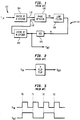
- FIG. 1 is a block diagram of a conventional circuit 102 which performs this function.
- the circuit 102 of Figure 1 includes a phase locked loop 114 having a phase detector 106, a loop filter 108, and a voltage controlled oscillator (VCO) 110.
- VCO voltage controlled oscillator
- Phase locked loops are well known and, thus, the structure and operation of the phase locked loop 114 contained in the circuit 102 of Figure 1 will be apparent to persons skilled in the relevant art. It is noted that phase locked loops are discussed in many publicly available documents, such as Phase Locked Loops by R.E. Best (McGraw Hill, New York, 1984).
- the circuit 102 of Figure 1 also includes a "divide by N” divider 104 (hereafter called the “N divider”) and a “divide by M” divider 112 (hereafter called the “M divider”).
- the N divider 104 operates to generate an output signal from an input signal, wherein the frequency of the output signal is equal to the frequency of the input signal divided by N.
- the M divider 112 operates to generate an output signal from an input signal, wherein the frequency of the output signal is equal to the frequency of the input signal divided by M.
- the dividers 104 and 112 can be implemented using a trigger (or T) flip flop (see Figure 2), whose output signal S OUT changes state with each rising edge of its input signal S IN (see Figure 3).
- a divide by two divider that is, where N and/or M equals 2
- T flip flops can be combined and used to implement dividers for other values of N and M will be apparent to persons skilled in the relevant art.
- the N divider 104 and the M divider 112 operate to modify an input signal F IN (which is generated from a reference clock, not shown) and an output signal F OUT in the manner described above. These modified signals are transferred to the phase detector 106 and, consequently, these modified signals are processed by the phase locked loop 114 in a well known manner.
- F IN is a signal having a fixed frequency
- the N divider 104 and the M divider 112 are implemented such that the values of N and M can be dynamically adjusted.
- the frequency of F OUT can be set to a particular frequency value by appropriately setting the values of N and M.
- Table 1 illustrates the frequencies which can be synthesized for particular values of N and M. For example, where N is 1 and M is 3, an output signal F OUT can be generated from an input signal F IN , wherein the frequency of F OUT is three times the frequency of F IN .
- phase locked loop circuits are plagued by many problems. These problems include jitter peaking, stability, acquisition behavior, and process variability. These and other problems of phase locked loop circuits are discussed in many publicly available documents, such as Phase Locked Loops , cited above.
- the conventional circuit 102 of Figure 1 enables one to generate, from a single reference clock, clock signals having frequencies which are different from the frequency of the reference clock.
- the conventional circuit 102 suffers from the same problems that plague phase locked loop circuits.
- a clock synthesizer which enables one to generate, from a single reference clock, clock signals having frequencies which are different from the frequency of the reference clock, and which does not suffer from the problems that plague phase locked loop based clock synthesizers.
- the present invention is directed to a delay-locked-loop based clock synthesizer for generating, from a reference signal, a clock signal having a frequency different from a frequency of the reference signal.
- the clock synthesizer of the present invention includes a delay-locked-loop circuit.
- the delay-locked-loop circuit includes a plurality of controllable delay elements serially connected to one another. Each of the delay elements delays the reference signal by an adjustable quantum of time such that the delay elements generate a plurality of delayed signals offset in time from one another and from the reference signal.
- a first multiplexer which is coupled to one or more of the delay elements, receives the delayed signals generated by the one or more of the delay elements, and routes one of the received delayed signals to an output of the first multiplexer.
- a phase detector which is connected to the output of the first multiplexer, receives the routed delayed signal and the reference signal, and generates a control signal indicative of a difference between a phase of the routed delayed signal and a phase of the reference signal.
- the delay-locked-loop circuit also includes a feedback loop, connected to the delay elements and the phase detector, for transferring the control signal from the phase detector to the delay elements.
- Each of the delay elements adjusts, in accordance with the control signal, the quantum of time by which they each delay the reference signal, such that the phase of the reference signal is synchronized with the phase of the routed delayed signal.
- the clock synthesizer also includes one or more mixing circuits, wherein each of the mixing circuits is connected to the controllable delay circuit and is associated with one of the one or more delay elements.
- the mixing circuits include combinational networks for logically combining the delayed signals such that the mixing circuits generate logically combined signals.
- the clock synthesizer further includes a second multiplexer, connected to the mixing circuits, for receiving the logically combined signals and for routing one of the received logically combined signals to an output of the second multiplexer, wherein the routed logically combined signal represents the clock signal.
- the present invention is directed to a clock synthesizer for synthesizing frequencies which are different from a reference clock frequency.
- the present invention is directed to a clock synthesizer for generating, from a single reference clock, clock signals having frequencies which are different from each other, and different from the frequency of the reference clock.
- the clock synthesizer of the present invention does not suffer from the problems that plague phase locked loop based clock synthesizers.
- FIG. 4 is a block diagram of a clock synthesizer 402 according to a preferred embodiment of the present invention.
- a reference clock (not shown), which is preferably a crystal oscillator, generates an input signal F IN (also called herein a reference clock signal), wherein the input signal F IN has a predetermined frequency.
- F IN also called herein a reference clock signal
- clock frequency requirements vary among applications.
- the value of the predetermined frequency of the input signal F IN is implementation dependent.
- the clock synthesizer 402 operates generally as follows.
- the clock synthesizer 402 generates an output signal F OUT from the input signal F IN , wherein the frequency of the output signal F OUT is different from the predetermined frequency of the input signal F IN . More particularly, the frequency of the output signal F OUT is an integer or non-integer multiple (or fraction) of the predetermined frequency of the input signal F IN .
- This integer or non-integer multiple (or fraction) by which the frequency of the output signal F OUT varies from the predetermined frequency of the input signal F IN may be dynamically adjusted, such that the frequency of the output signal F OUT may be dynamically adjusted.
- the clock synthesizer 402 of the present invention synthesizes frequencies which differ from each other, and which differ from the frequency of the reference clock signal. The clock synthesizer 402 shall now be described in detail.
- the clock synthesizer 402 includes a "Divide by N” divider 404 (hereafter call the "N divider") which receives the input signal F IN
- the N divider 404 is similar in structure and operation to the N divider 104 and the M divider 112 shown in Figure 1, and discussed above.
- the N divider 404 operates to generate a modified input signal F IN ' from the input signal F IN , wherein the frequency of the modified input signal F IN ' is equal to the frequency of the input signal F IN divided by N.
- the N divider 404 enables the clock synthesizer 402 to synthesize a broader range of frequencies.
- the modified input signal F IN ' is transferred to a delay locked loop 408.
- Delay locked loops are generally well known, and are discussed in many publicly available documents, such as "A Monolithic CMOS 10 MHz DPLL For Burst-Mode Data” by Research and Leonowich ( ISSCC Digest , 1990), which is herein incorporated by reference in its entirety.
- the delay locked loop 408 is similar in structure to a phase locked loop, and operates in the same way as a phase locked loop.
- a controllable delay line comprising a plurality of controllable delay elements 406 has replaced the voltage controlled oscillator (VCO) of the phase locked loop.
- VCO voltage controlled oscillator
- the problems which plague phase locked loop are due to the VCO contained therein. Since the delay locked loop 408 does not include a VCO, the delay locked loop 408 does not suffer from the problems which plague phase locked loops. Consequently, since the clock synthesizer 402 of the present invention is based on a delay locked loop, rather than a phase locked loop, the clock synthesizer 402 of the present invention does not suffer from the problems which plague phase locked loop-based clock synthesizers.
- the modified input signal F IN ' is received by a delay element 406A.
- the delay element 406A delays the modified input signal F IN ' by a quantum of time to produce a signal at a node 420, which differs in phase from the modified input signal F IN ' by the quantum of time.
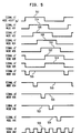
- a signal 502 represents the signal present at a node 418 (that is, the modified input signal F IN ') and a signal 504 represents the signal at the node 420 generated by the delay element 406A.
- Each delay element 406 delays an input signal which it receives by a quantum of time to generate an output signal which differs in phase from its input signal by the quantum of time.
- a signal 506 represents the signal present at a node 422 generated by the delay element 406B
- a signal 508 represents the signal present at a node 424 generated by the delay element 406C
- a signal 510 represents the signal present at a node 426 generated by the delay element 406D
- a signal 512 represents the signal present at a node 428 generated by the delay element 406E.
- the quantum of time introduced by each of the delay elements 406 is the same.
- the delay elements 406 are controllable, such that the amount of delay introduced by each is adjustable.
- the delay elements 406 can be implemented in any number of ways.
- the delay elements 406 can be implemented using a combination of multiplexers, inverters, and/or registers. Persons skilled in the relevant art will find it apparent to implement controllable delay elements, particularly in light of the publicly available documents which discuss controllable delay elements, such as "A Monolithic CMOS 10 MHz DPLL For Burst-Mode Data," cited above.
- An inverter 416 inverts the modified input signal F IN '.
- This inverted modified input signal which is present at a node 429, is shown in Figure 5 as a signal 514.
- a phase detector 412 receives the signal generated by the delay element 406E and present at the node 428 (that is, the signal 512 in Figure 5). The phase detector 412 also receives the inverted modified input signal which is present at the node 429 (that is, the signal 514 in Figure 5).
- phase detector 412 compares the phase of the signal 512 to the phase of the signal 514 (preferably, the phase detector 412 operates to match a rising edge of the signal 512 to a rising edge of the signal 514), and generates an error voltage Ve, wherein the magnitude of the error voltage Ve is proportional to the difference in phase between these two signals 512 and 514.
- the error voltage Ve is processed in a well known manner by a loop filter 414 to produce a control voltage Vc [ WHAT DOES THE LOOP FILTER DO? ].
- Vc control voltage
- the magnitude of the control voltage Vc is proportional to the difference in phase between the signal 512 and the signal 514.
- the control voltage Vc is transferred to each of the delay elements 406, and causes the delay elements 406 to modify the amount of delay which they each introduce.
- the error voltage Ve and the control voltage Vc will be substantially equal to zero volts.
- the delay elements 406 do not modify the amount of delay which they each introduced.
- the error voltage Ve and the control voltage Vc each have a non-zero magnitude which is proportional to this phase difference.
- the delay elements 406 modify the amount of delay which they introduce in accordance with the non-zero magnitude of the control voltage Vc. In this manner, the phase detector 412 controls the amount of delay which the delay elements 406 introduce such that the phase of the signal 512 present at the node 428 is equal to the phase of the signal 514 present at the node 429.
- the signals shown in Figure 5 are those which are generated after the delay locked loop 408 has reached a "steady state.” That is, the signals in Figure 5 are those which are generated after the phase detector 412 has adjusted the amount of delay introduced by the delay elements 406 such that the phase of the signal 512 is equal to the phase of the signal 514.
- the phase detector 412 preferably operates to match the phase of the signal 512 to the phase of the signal 514 after the passage of one half a period of the modified input signal F IN '. Consequently, the amount of time delay introduced by each of the delay elements 406 when the delay locked loop is in the "steady state" condition is represented by the following equation: 1/(2*frequency(F IN ')*X), where X is the number of delay elements 406 in the delay locked loop 408 (in the embodiment of Figure 4, X is equal to five).
- the phase detector 412 could be implemented such that it matches the phase of the signal 512 present at the node 428 to the phase of the signal 514 present at the node 429 after other predetermined time periods, such as after the passage of one full period of the modified input signal F IN '.
- the amount of time delay introduced by each of the delay elements 406 when the delay locked loop is in the "steady state" condition is represented by the following equation: 1/(frequency(F IN ')*X).
- the signals 502-512 have the same frequency but different phases.
- the delay locked loop 408 by itself, cannot synthesize clock frequencies which are different from the frequency of the reference clock signal F IN .
- delay locked loops are used for purposes other than frequency synthesization, such as pulse shaping a transmitted wave (this operation is sometimes called “pre-distortion”).
- Conventional uses of delay locked loops are described in "A Monolithic CMOS 10 MHz DPLL For Burst-Mode Data," cited above.
- a mixing circuit 410 is used to generate, from the signals 502-512 generated by the delay locked loop 408, a clock signal 526 having a frequency which is different from the frequency of the reference clock signal F IN and which is different from the frequency of the modified reference clock signal F IN ' (signal 502).
- the mixing circuit 410 shall now be described.
- the mixing circuit 410 includes NAND gates 442, 444, 446, 448, 450, and 460 (the bubbles at some of the inputs of these NAND gates represent inverters). These NAND gates 442, 444, 446, 448, 450, 460 are interconnected and receive the signals 502-512 generated by the delay locked loop 408 such that the mixing circuit 410 generates a clock signal 526 having a frequency which is different from the frequencies of the reference clock signal F IN and the modified reference clock signal F IN '.
- the signal 502 present at the node 418 is applied to the NAND gate 442.
- the signal 504 at the node 420 is inverted and applied to the NAND gate 442.
- the NAND gate 442 performs the well known "NAND” logical operation using these two signals to thereby produce a signal 516 ( Figure 5), which is present at a node 432, and which is applied to the NAND gate 460.
- the NAND gate 444 produces a signal 522, which is present at a node 438, and which is applied to the NAND gate 460.
- the NAND gate 446 produces a signal 518, which is present at a node 434, and which is applied to the NAND gate 460.
- the NAND gate 448 produces a signal 520, which is present at a node 436, and which is applied to the NAND gate 460.
- the NAND gate 450 produces a signal 524, which is present at a node 440, and which is applied to the NAND gate 460.
- the NAND gate 460 performs the well known "NAND" operation using these signals 432-440 discussed above to thereby produce a signal 526, which is present at a node 462, and which represents the output signal F OUT .
- the frequency of the output signal F OUT is five times the frequency of the modified input signal F IN '.
- mixing circuit 402 could be alternatively implemented using a combinational network different from that shown in Figure 4.
- the structure and operation of such alternative combinational networks will be apparent to persons skilled in the relevant art.
- the N divider 404 enables the clock synthesizer 402 to synthesize a broader range of frequencies. This is the case, since the N divider 404 generates a modified input signal F IN ' from the input signal F IN , wherein the frequency of the modified input signal F IN ' is equal to the frequency of the input signal F IN divided by N.
- Table 2 illustrates the frequencies which can be synthesized for particular values of N using the clock synthesizer 402 shown in Figure 4. For example, where N is 1, the frequency of F OUT is five times the frequency of F IN (this is the case shown in Figure 5).
- the clock synthesizer 402 of Figure 4 is limited relative to the phase locked loop synthesizer 102 (shown in Figure 1) in the number of frequencies which it can synthesize from the reference clock frequency (that is, from the frequency of the input signal F IN ).
- the clock synthesizer 402 of Figure 4 cannot synthesize the frequencies corresponding to M equals 3 and M equals 4 shown in Table 1. This is the case, since there are no phase transitions at the appropriate times in a five tap delay locked loop (that is, a delay locked loop having five delay elements).
- these frequencies can be synthesized using three and four tap delay locked loops (in combination with mixing circuits), since such delay locked loops produce signals having phase transitions which occur at the appropriate times. This is described in detail below.
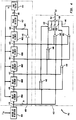
- FIG. 6 is a block diagram of a clock synthesizer 601 according to an alternate embodiment of the present invention.
- a reference clock (not shown), which is preferably a crystal oscillator, generates an input signal, or reference clock signal, F IN .
- the clock synthesizer 601 includes a "Divide by N” divider 404 (hereafter call the “N divider") which is identical in structure and operation to the N divider 404 shown in Figure 4.
- the N divider operates to generate a modified input signal F IN ' from the input signal F IN , wherein the frequency of the modified input signal F IN ' is equal to the frequency of the input signal F IN divided by N.
- the modified input signal F IN ' is transferred to a delay locked loop 603.
- the delay locked loop 603 shown in Figure 6 is similar in operation and structure to the delay locked loop 408 shown in Figure 4. The differences between these two delay locked loops 408, 603 shall now be discussed.
- the delay locked loop 603 shown in Figure 6 includes a multiplexer 602 which is positioned between the delay elements 406C, 406D, 406E and the phase detector 412.
- the multiplexer 602 routes to the phase detector 412 either the signal output by the delay element 406C (and present at the node 424), the signal output by the delay element 406D (and present at the node 426), or the signal output by the delay element 406E (and present at the node 428).
- the phase detector 412 also receives the inverted modified input signal.
- the phase detector 412 operates to check whether the phase of the signal present at the node 428 is substantially equal to the phase of the signal present at the node 429 (for reference purposes, this is called the five tap case).
- all five of the delay elements 406 are used to ultimately produce the signal present at the node 428, wherein each of the delay elements 406 introduces a time delay of 1/(2*frequency(F IN ')*5).
- the signals produced by the delay elements 406 are shown as 504, 506, 508, 510, and 512 in Figure 5.
- the phase detector 412 When the multiplexer 602 routes to the phase detector 412 the signal output by the delay element 406D (and present at the node 426), the phase detector 412 operates to check whether the phase of the signal present at the node 426 is substantially equal to the phase of the signal present at the node 429 (for reference purposes, this is called the four tap case). Note that only four of the delay elements 406A-406D are used to ultimately produce the signal present at the node 426, wherein each of these four delay elements 406A-406D introduces a time delay of 1/(2*frequency(F IN ' )*4). In the four tap case, the signals produced by the delay elements 406A-406D are shown as 804, 806, 808, and 810 in Figure 8.
- the phase detector 412 When the multiplexer 602 routes to the phase detector 412 the signal output by the delay element 406C (and present at the node 424), the phase detector 412 operates to check whether the phase of the signal present at the node 424 is substantially equal to the phase of the signal present at the node 429 (for reference purposes, this is called the three tap case). Note that only three of the delay elements 406A-406C are used to ultimately produce the signal present at the node 424, wherein each of these three delay elements 406A-406C introduces a time delay of 1/(2*frequency(F IN ')*3). The shape of the signals produced by the delay elements 406A406C in the three tap case will be apparent to persons skilled in the relevant art based on the teachings contained herein.
- the phase of the signals produced in the three tap case is different than the phases of the signals produced in the four and five tap case. Consequently, frequencies which cannot be synthesized in the four and five tap cases can be synthesized in the three tap case.
- the clock synthesizer 601 includes three mixing circuits 604, 608, and 410. Each of the mixing circuits 604, 608, and 410 is used to generate, from the signals generated by the delay locked loop 603, a clock signal having a frequency which is different from the frequency of the reference clock signal F IN , and which is different from the frequency of the modified reference clock signal F IN '.
- the mixing circuit 410 generates a clock signal having a frequency which is different from the frequencies of the reference clock signal F IN and the modified reference clock signal F IN '.
- the signals generated by the mixing circuits 604 and 610 are ignored (as described below).
- the mixing circuit 608 generates a clock signal having a frequency which is different from the frequencies of the reference clock signal F IN and the modified reference clock signal F IN '.
- the signals generated by the mixing circuits 604 and 410 are ignored.
- the mixing circuit 604 generates a clock signal having a frequency which is different from the frequencies of the reference clock signal F IN and the modified reference clock signal F IN '.
- the signals generated by the mixing circuits 608 and 410 are ignored.
- a multiplexer 612 receives the signals generated by the mixing circuits 604, 608, 410.
- the multiplexer 612 routes one of these signals to a node 614. This signal present at node 614 is the output signal F OUT .
- the routing functions performed by the multiplexers 602 and 612 are controlled by a single control signal 616.
- the control signal 616 is generated by a control mechanism (not shown), which determines whether the clock synthesizer 601 operates in the three tap case, the four tap case, or the five tap case.
- the control mechanism preferably adjusts to the clock frequency needs of the system in which it is contained and, therefore, the control mechanism is implementation dependent.
- the control mechanism determines that the clock synthesizer 601 should operate in the three tap case, the control mechanism generates the control signal 616 such that the multiplexer 602 routes the signal present at node 424 to the phase detector 412, and such that the multiplexer 612 routes the signal generated by the mixing circuit 604 to the node 614.
- control mechanism determines that the clock synthesizer 601 should operate in the four tap case, the control mechanism generates the control signal 616 such that the multiplexer 602 routes the signal present at node 426 to the phase detector 412, and such that the multiplexer 612 routes the signal generated by the mixing circuit 608 to the node 614.
- control mechanism determines that the clock synthesizer 601 should operate in the five tap case, the control mechanism generates the control signal 616 such that the multiplexer 602 routes the signal present at node 428 to the phase detector 412, and such that the multiplexer 612 routes the signal generated by the mixing circuit 410 to the node 614.
- the mixing circuits 604, 608, and 410 shall now be described.
- the mixing circuit 410 can be implemented using various combinational networks. The structure and operation of such combinational networks will be apparent to persons skilled in the relevant art.
- One combinational network which can be used to implement the mixing circuit 410 is shown in Figure 4 (described above).
- the mixing circuit 608 can be implemented using various combinational networks. The structure and operation of such combinational networks will be apparent to persons skilled in the relevant art.
- One combinational network which can be used to implement the mixing circuit 608 is shown in Figure 7, and shall now be described. Recall that the signals produced by the delay elements 406A-406D during the four tap case are shown as 804, 806, 808, and 810 in Figure 8.
- the mixing circuit 608 includes exclusive-OR gates 702, 704 and an OR gate 706. These gates 702, 704, 706 are interconnected and receive the signals present at nodes 418, 420, 422, and 424 (note that the signal present at node 426 is not used by the mixing circuit 608), such that the mixing circuit 608 generates a clock signal having a frequency which is different from the frequencies of the reference clock signal F IN and the modified reference clock signal F IN '.
- the signals present at nodes 418 and 420 are applied to the exclusive-OR gate 702.
- the exclusive-OR gate 702 performs the well known "exclusive-OR" logical operation using these two signals to thereby produce a signal 814, which is present at a node 708, and which is applied to the OR gate 610.
- the exclusive-OR gate 704 produces a signal 816, which is present at a node 710, and which is applied to the OR gate 610.
- the OR gate 706 performs the well known "OR" logical operation using these signals 814, 816 discussed above to thereby produce a signal 818, which is present at a node 610, and which represents the output signal F OUT during the four tap case.
- the frequency of F OUT is four times the frequency of F IN '.
- the mixing circuit 604 can be implemented using various combinational networks. The structure and operation of such combinational networks will be apparent to persons skilled in the relevant art.
- the mixing circuit 604 could be implemented by using the combinational network shown in Figure 4, except that nodes 436 and 440 are forced to a high logical state in a well known manner. In this manner, the frequency of F OUT with be three times the frequency of F IN '.
- the clock synthesizer 601 can synthesize all of the frequencies shown in Table 1. Additional frequencies can be synthesized by modifying the combinational logic of the mixing circuits 410, 604, 610. Such modifications will be apparent to persons skilled in the relevant art.
Abstract
A delay-locked-loop based clock synthesizer for generating, from a reference signal, a clock signal having a frequency different from a frequency of the reference signal includes a delay-locked-loop circuit having a plurality of controllable delay elements serially connected to one another. Each of the delay elements delays the reference signal by an adjustable quantum of time such that the delay elements generate a plurality of delayed signals. A first multiplexer routes one of the delayed signals to a phase detector, which generates a control signal indicative of a difference between a phase of the routed delayed signal and a phase of the reference signal. A feedback loop transfers the control signal from the phase detector to the delay elements, wherein each of the delay elements adjusts, in accordance with the control signal, the quantum of time by which they each delay the reference signal, such that the phase of the reference signal is synchronized with the phase of the routed delayed signal. The clock synthesizer also includes one or more mixing circuits for logically combining the delayed signals such that the mixing circuits generate logically combined signals. A second multiplexer routes one of the received logically combined signals to an output of the second multiplexer, wherein the routed logically combined signal represents the clock signal.
Description
- The present invention relates generally to clock synthesizers for generating clock signals, and more particularly, to clock synthesizers which are implemented using delay locked loops having a dynamically adjustable number of delay elements located therein.
- A clock synthesizer generates a clock signal having a particular frequency from a reference clock, such as a crystal oscillator. As will be appreciated, it is often desirable to have the ability to generate, from a single reference clock, clock signals having frequencies which are different from the frequency of the reference clock. In other words, it is often desirable to have the ability to synthesize multiple clock frequencies from a single reference clock frequency.
- Figure 1 is a block diagram of a
conventional circuit 102 which performs this function. Thecircuit 102 of Figure 1 includes a phase lockedloop 114 having aphase detector 106, aloop filter 108, and a voltage controlled oscillator (VCO) 110. - Phase locked loops are well known and, thus, the structure and operation of the phase locked
loop 114 contained in thecircuit 102 of Figure 1 will be apparent to persons skilled in the relevant art. It is noted that phase locked loops are discussed in many publicly available documents, such as Phase Locked Loops by R.E. Best (McGraw Hill, New York, 1984). - The
circuit 102 of Figure 1 also includes a "divide by N" divider 104 (hereafter called the "N divider") and a "divide by M" divider 112 (hereafter called the "M divider"). TheN divider 104 operates to generate an output signal from an input signal, wherein the frequency of the output signal is equal to the frequency of the input signal divided by N. Similarly, theM divider 112 operates to generate an output signal from an input signal, wherein the frequency of the output signal is equal to the frequency of the input signal divided by M. - The
dividers - Referring again to Figure 1, the
N divider 104 and theM divider 112 operate to modify an input signal FIN (which is generated from a reference clock, not shown) and an output signal FOUT in the manner described above. These modified signals are transferred to thephase detector 106 and, consequently, these modified signals are processed by the phase lockedloop 114 in a well known manner. The frequency of the output signal FOUT can be described by the following relationship:
- Typically, FIN is a signal having a fixed frequency, and the
N divider 104 and theM divider 112 are implemented such that the values of N and M can be dynamically adjusted. Thus, the frequency of FOUT can be set to a particular frequency value by appropriately setting the values of N and M. Table 1 illustrates the frequencies which can be synthesized for particular values of N and M. For example, where N is 1 and M is 3, an output signal FOUT can be generated from an input signal FIN, wherein the frequency of FOUT is three times the frequency of FIN.Table 1: Available Frequency Synthesizer Frequencies N M frequency(FOUT)/frequency(FIN) 1 3 3 2 3 1.5 3 3 1 1 4 4 2 4 2 3 4 1.333 1 5 5 2 5 2.5 3 5 1.667 - As is well known, phase locked loop circuits are plagued by many problems. These problems include jitter peaking, stability, acquisition behavior, and process variability. These and other problems of phase locked loop circuits are discussed in many publicly available documents, such as Phase Locked Loops, cited above.
- As is clear from the discussion above, the
conventional circuit 102 of Figure 1 enables one to generate, from a single reference clock, clock signals having frequencies which are different from the frequency of the reference clock. However, since it utilizes a phase lockedloop 114, theconventional circuit 102 suffers from the same problems that plague phase locked loop circuits. - Thus, what is required is a clock synthesizer which enables one to generate, from a single reference clock, clock signals having frequencies which are different from the frequency of the reference clock, and which does not suffer from the problems that plague phase locked loop based clock synthesizers.
- The present invention is directed to a delay-locked-loop based clock synthesizer for generating, from a reference signal, a clock signal having a frequency different from a frequency of the reference signal. The clock synthesizer of the present invention includes a delay-locked-loop circuit.
- The delay-locked-loop circuit includes a plurality of controllable delay elements serially connected to one another. Each of the delay elements delays the reference signal by an adjustable quantum of time such that the delay elements generate a plurality of delayed signals offset in time from one another and from the reference signal.
- A first multiplexer, which is coupled to one or more of the delay elements, receives the delayed signals generated by the one or more of the delay elements, and routes one of the received delayed signals to an output of the first multiplexer. A phase detector, which is connected to the output of the first multiplexer, receives the routed delayed signal and the reference signal, and generates a control signal indicative of a difference between a phase of the routed delayed signal and a phase of the reference signal.
- The delay-locked-loop circuit also includes a feedback loop, connected to the delay elements and the phase detector, for transferring the control signal from the phase detector to the delay elements. Each of the delay elements adjusts, in accordance with the control signal, the quantum of time by which they each delay the reference signal, such that the phase of the reference signal is synchronized with the phase of the routed delayed signal.
- The clock synthesizer also includes one or more mixing circuits, wherein each of the mixing circuits is connected to the controllable delay circuit and is associated with one of the one or more delay elements. The mixing circuits include combinational networks for logically combining the delayed signals such that the mixing circuits generate logically combined signals.
- The clock synthesizer further includes a second multiplexer, connected to the mixing circuits, for receiving the logically combined signals and for routing one of the received logically combined signals to an output of the second multiplexer, wherein the routed logically combined signal represents the clock signal.
- Further features and advantages of the present invention, as well as the structure and operation of various embodiments of the present invention, are described in detail below with reference to the accompanying drawings. In the drawings, like reference numbers indicate identical or functionally similar elements.
- The present invention will be described with reference to the accompanying drawings, wherein:
- Figure 1 is a block diagram of a conventional phase locked loop-based clock synthesizer;
- Figure 2 is a block diagram of a conventional divider which is implemented using a trigger flip flop;
- Figure 3 shows signals used to illustrate the operation of the divider of Figure 2;
- Figure 4 is a block diagram of a delay locked loop-based clock synthesizer according to a preferred embodiment of the present invention;
- Figure 5 shows signals used to illustrate the operation of the clock synthesizer of Figure 4;
- Figure 6 is a block diagram of a delay locked loop-based clock synthesizer according to an alternate embodiment of the present invention;
- Figure 7 is a block diagram of a mixing circuit which represents an element of the clock synthesizer of Figure 6; and
- Figure 8 shows signals used to illustrate the operation of the clock synthesizer of Figure 6.
- The present invention is directed to a clock synthesizer for synthesizing frequencies which are different from a reference clock frequency. In other words, the present invention is directed to a clock synthesizer for generating, from a single reference clock, clock signals having frequencies which are different from each other, and different from the frequency of the reference clock. The clock synthesizer of the present invention does not suffer from the problems that plague phase locked loop based clock synthesizers.
- Figure 4 is a block diagram of a
clock synthesizer 402 according to a preferred embodiment of the present invention. A reference clock (not shown), which is preferably a crystal oscillator, generates an input signal FIN (also called herein a reference clock signal), wherein the input signal FIN has a predetermined frequency. As will be appreciated, clock frequency requirements vary among applications. Thus, the value of the predetermined frequency of the input signal FIN is implementation dependent. - The
clock synthesizer 402 operates generally as follows. Theclock synthesizer 402 generates an output signal FOUT from the input signal FIN, wherein the frequency of the output signal FOUT is different from the predetermined frequency of the input signal FIN. More particularly, the frequency of the output signal FOUT is an integer or non-integer multiple (or fraction) of the predetermined frequency of the input signal FIN. - This integer or non-integer multiple (or fraction) by which the frequency of the output signal FOUT varies from the predetermined frequency of the input signal FIN may be dynamically adjusted, such that the frequency of the output signal FOUT may be dynamically adjusted. In this manner, the
clock synthesizer 402 of the present invention synthesizes frequencies which differ from each other, and which differ from the frequency of the reference clock signal. Theclock synthesizer 402 shall now be described in detail. - The
clock synthesizer 402 includes a "Divide by N" divider 404 (hereafter call the "N divider") which receives the input signal FIN TheN divider 404 is similar in structure and operation to theN divider 104 and theM divider 112 shown in Figure 1, and discussed above. TheN divider 404 operates to generate a modified input signal FIN' from the input signal FIN, wherein the frequency of the modified input signal FIN' is equal to the frequency of the input signal FIN divided by N. As discussed further below, theN divider 404 enables theclock synthesizer 402 to synthesize a broader range of frequencies. - The modified input signal FIN' is transferred to a delay locked
loop 408. Delay locked loops are generally well known, and are discussed in many publicly available documents, such as "A Monolithic CMOS 10 MHz DPLL For Burst-Mode Data" by Sonntag and Leonowich (ISSCC Digest, 1990), which is herein incorporated by reference in its entirety. - The delay locked
loop 408 is similar in structure to a phase locked loop, and operates in the same way as a phase locked loop. In the delay lockedloop 408, however, a controllable delay line comprising a plurality of controllable delay elements 406 has replaced the voltage controlled oscillator (VCO) of the phase locked loop. - As will be appreciated, the problems (such as jitter peaking, stability, acquisition behavior, and process variability) which plague phase locked loop are due to the VCO contained therein. Since the delay locked
loop 408 does not include a VCO, the delay lockedloop 408 does not suffer from the problems which plague phase locked loops. Consequently, since theclock synthesizer 402 of the present invention is based on a delay locked loop, rather than a phase locked loop, theclock synthesizer 402 of the present invention does not suffer from the problems which plague phase locked loop-based clock synthesizers. - The operation of the delay locked
loop 408 shall now be described. - The modified input signal FIN' is received by a
delay element 406A. Thedelay element 406A delays the modified input signal FIN' by a quantum of time to produce a signal at anode 420, which differs in phase from the modified input signal FIN' by the quantum of time. This is shown in Figure 5, wherein asignal 502 represents the signal present at a node 418 (that is, the modified input signal FIN') and asignal 504 represents the signal at thenode 420 generated by thedelay element 406A. - The operation of the
other delay elements delay element 406A. Each delay element 406 delays an input signal which it receives by a quantum of time to generate an output signal which differs in phase from its input signal by the quantum of time. This is shown in Figure 5, wherein asignal 506 represents the signal present at anode 422 generated by the delay element 406B, asignal 508 represents the signal present at anode 424 generated by thedelay element 406C, asignal 510 represents the signal present at anode 426 generated by the delay element 406D, and asignal 512 represents the signal present at anode 428 generated by thedelay element 406E. - The quantum of time introduced by each of the delay elements 406 is the same. The delay elements 406 are controllable, such that the amount of delay introduced by each is adjustable.
- The delay elements 406 can be implemented in any number of ways. For example, the delay elements 406 can be implemented using a combination of multiplexers, inverters, and/or registers. Persons skilled in the relevant art will find it apparent to implement controllable delay elements, particularly in light of the publicly available documents which discuss controllable delay elements, such as "A Monolithic CMOS 10 MHz DPLL For Burst-Mode Data," cited above.
- An
inverter 416 inverts the modified input signal FIN'. This inverted modified input signal, which is present at anode 429, is shown in Figure 5 as asignal 514. - A
phase detector 412 receives the signal generated by thedelay element 406E and present at the node 428 (that is, thesignal 512 in Figure 5). Thephase detector 412 also receives the inverted modified input signal which is present at the node 429 (that is, thesignal 514 in Figure 5). - The structure and operation of phase detectors are well known. The
phase detector 412 compares the phase of thesignal 512 to the phase of the signal 514 (preferably, thephase detector 412 operates to match a rising edge of thesignal 512 to a rising edge of the signal 514), and generates an error voltage Ve, wherein the magnitude of the error voltage Ve is proportional to the difference in phase between these twosignals - The error voltage Ve is processed in a well known manner by a
loop filter 414 to produce a control voltage Vc [WHAT DOES THE LOOP FILTER DO?]. Like the error voltage Ve, the magnitude of the control voltage Vc is proportional to the difference in phase between thesignal 512 and thesignal 514. - The control voltage Vc is transferred to each of the delay elements 406, and causes the delay elements 406 to modify the amount of delay which they each introduce. When the
signal 512 present at thenode 428 is equal in phase to thesignal 514 present at thenode 429, the error voltage Ve and the control voltage Vc will be substantially equal to zero volts. When the control voltage Vc is equal to zero volts, the delay elements 406 do not modify the amount of delay which they each introduced. - When the
signal 512 present at thenode 428 is not equal in phase to thesignal 514 present at thenode 429, the error voltage Ve and the control voltage Vc each have a non-zero magnitude which is proportional to this phase difference. Upon receiving the control voltage Vc, the delay elements 406 modify the amount of delay which they introduce in accordance with the non-zero magnitude of the control voltage Vc. In this manner, thephase detector 412 controls the amount of delay which the delay elements 406 introduce such that the phase of thesignal 512 present at thenode 428 is equal to the phase of thesignal 514 present at thenode 429. - The signals shown in Figure 5 are those which are generated after the delay locked
loop 408 has reached a "steady state." That is, the signals in Figure 5 are those which are generated after thephase detector 412 has adjusted the amount of delay introduced by the delay elements 406 such that the phase of thesignal 512 is equal to the phase of thesignal 514. - As apparent from Figure 5, the
phase detector 412 preferably operates to match the phase of thesignal 512 to the phase of thesignal 514 after the passage of one half a period of the modified input signal FIN'. Consequently, the amount of time delay introduced by each of the delay elements 406 when the delay locked loop is in the "steady state" condition is represented by the following equation: 1/(2*frequency(FIN')*X), where X is the number of delay elements 406 in the delay locked loop 408 (in the embodiment of Figure 4, X is equal to five). - Alternatively, the
phase detector 412 could be implemented such that it matches the phase of thesignal 512 present at thenode 428 to the phase of thesignal 514 present at thenode 429 after other predetermined time periods, such as after the passage of one full period of the modified input signal FIN'. In this case, the amount of time delay introduced by each of the delay elements 406 when the delay locked loop is in the "steady state" condition is represented by the following equation:
- The signals 502-512 have the same frequency but different phases. Thus, the delay locked
loop 408, by itself, cannot synthesize clock frequencies which are different from the frequency of the reference clock signal FIN. Conventionally, delay locked loops are used for purposes other than frequency synthesization, such as pulse shaping a transmitted wave (this operation is sometimes called "pre-distortion"). Conventional uses of delay locked loops are described in "A Monolithic CMOS 10 MHz DPLL For Burst-Mode Data," cited above. - According to the present invention, a
mixing circuit 410 is used to generate, from the signals 502-512 generated by the delay lockedloop 408, aclock signal 526 having a frequency which is different from the frequency of the reference clock signal FIN and which is different from the frequency of the modified reference clock signal FIN' (signal 502). The mixingcircuit 410 shall now be described. - The mixing
circuit 410 includesNAND gates NAND gates loop 408 such that the mixingcircuit 410 generates aclock signal 526 having a frequency which is different from the frequencies of the reference clock signal FIN and the modified reference clock signal FIN'. - Specifically, the
signal 502 present at thenode 418 is applied to theNAND gate 442. Also, thesignal 504 at thenode 420 is inverted and applied to theNAND gate 442. TheNAND gate 442 performs the well known "NAND" logical operation using these two signals to thereby produce a signal 516 (Figure 5), which is present at anode 432, and which is applied to theNAND gate 460. - In a similar manner, the
NAND gate 444 produces asignal 522, which is present at anode 438, and which is applied to theNAND gate 460. TheNAND gate 446 produces asignal 518, which is present at anode 434, and which is applied to theNAND gate 460. TheNAND gate 448 produces asignal 520, which is present at anode 436, and which is applied to theNAND gate 460. TheNAND gate 450 produces asignal 524, which is present at anode 440, and which is applied to theNAND gate 460. - The
NAND gate 460 performs the well known "NAND" operation using these signals 432-440 discussed above to thereby produce asignal 526, which is present at anode 462, and which represents the output signal FOUT. As is apparent from Figure 5, the frequency of the output signal FOUT is five times the frequency of the modified input signal FIN'. - It should be understood that the mixing
circuit 402 could be alternatively implemented using a combinational network different from that shown in Figure 4. The structure and operation of such alternative combinational networks will be apparent to persons skilled in the relevant art. - The
N divider 404 enables theclock synthesizer 402 to synthesize a broader range of frequencies. This is the case, since theN divider 404 generates a modified input signal FIN' from the input signal FIN, wherein the frequency of the modified input signal FIN' is equal to the frequency of the input signal FIN divided by N. Table 2 illustrates the frequencies which can be synthesized for particular values of N using theclock synthesizer 402 shown in Figure 4. For example, where N is 1, the frequency of FOUT is five times the frequency of FIN (this is the case shown in Figure 5).Table 2: Available Synthesizer Frequencies N frequency(F OUT )/frequency(F IN ) 1 5 2 2.5 3 1.667 - As apparent from an inspection of both Tables 1 and 2, the
clock synthesizer 402 of Figure 4 is limited relative to the phase locked loop synthesizer 102 (shown in Figure 1) in the number of frequencies which it can synthesize from the reference clock frequency (that is, from the frequency of the input signal FIN). In particular, theclock synthesizer 402 of Figure 4 cannot synthesize the frequencies corresponding to M equals 3 and M equals 4 shown in Table 1. This is the case, since there are no phase transitions at the appropriate times in a five tap delay locked loop (that is, a delay locked loop having five delay elements). However, these frequencies can be synthesized using three and four tap delay locked loops (in combination with mixing circuits), since such delay locked loops produce signals having phase transitions which occur at the appropriate times. This is described in detail below. - Figure 6 is a block diagram of a
clock synthesizer 601 according to an alternate embodiment of the present invention. A reference clock (not shown), which is preferably a crystal oscillator, generates an input signal, or reference clock signal, FIN. - The
clock synthesizer 601 includes a "Divide by N" divider 404 (hereafter call the "N divider") which is identical in structure and operation to theN divider 404 shown in Figure 4. The N divider operates to generate a modified input signal FIN' from the input signal FIN, wherein the frequency of the modified input signal FIN' is equal to the frequency of the input signal FIN divided by N. - The modified input signal FIN' is transferred to a delay locked
loop 603. The delay lockedloop 603 shown in Figure 6 is similar in operation and structure to the delay lockedloop 408 shown in Figure 4. The differences between these two delay lockedloops - In addition to the delay elements 406, the
phase detector 412, and theloop filter 414, the delay lockedloop 603 shown in Figure 6 includes amultiplexer 602 which is positioned between thedelay elements phase detector 412. Themultiplexer 602 routes to thephase detector 412 either the signal output by thedelay element 406C (and present at the node 424), the signal output by the delay element 406D (and present at the node 426), or the signal output by thedelay element 406E (and present at the node 428). - The
phase detector 412 also receives the inverted modified input signal. Thus, when themultiplexer 602 routes to thephase detector 412 the signal output by thedelay element 406E (and present at the node 428), thephase detector 412 operates to check whether the phase of the signal present at thenode 428 is substantially equal to the phase of the signal present at the node 429 (for reference purposes, this is called the five tap case). Note that all five of the delay elements 406 are used to ultimately produce the signal present at thenode 428, wherein each of the delay elements 406 introduces a time delay of 1/(2*frequency(FIN')*5). In the five tap case, the signals produced by the delay elements 406 are shown as 504, 506, 508, 510, and 512 in Figure 5. - When the multiplexer 602 routes to the
phase detector 412 the signal output by the delay element 406D (and present at the node 426), thephase detector 412 operates to check whether the phase of the signal present at thenode 426 is substantially equal to the phase of the signal present at the node 429 (for reference purposes, this is called the four tap case). Note that only four of thedelay elements 406A-406D are used to ultimately produce the signal present at thenode 426, wherein each of these fourdelay elements 406A-406D introduces a time delay of 1/(2*frequency(FIN ')*4). In the four tap case, the signals produced by thedelay elements 406A-406D are shown as 804, 806, 808, and 810 in Figure 8. - When the multiplexer 602 routes to the
phase detector 412 the signal output by thedelay element 406C (and present at the node 424), thephase detector 412 operates to check whether the phase of the signal present at thenode 424 is substantially equal to the phase of the signal present at the node 429 (for reference purposes, this is called the three tap case). Note that only three of thedelay elements 406A-406C are used to ultimately produce the signal present at thenode 424, wherein each of these threedelay elements 406A-406C introduces a time delay of 1/(2*frequency(FIN')*3). The shape of the signals produced by the delay elements 406A406C in the three tap case will be apparent to persons skilled in the relevant art based on the teachings contained herein. - Note that, since the time delay introduced by the delay elements 406 during the four tap case is different than during the five tap case (assuming the same frequency(FIN') in both cases), the phase of the signals produced in the four tap case is different than the phase of the signals produced in the five tap case. Consequently, frequencies which cannot be synthesized in the five tap case can be synthesized in the four tap case.
- Similarly, since the time delay introduced by the delay elements 406 during the three tap case is different than during the four and five tap cases (assuming the same frequency(FIN') in both cases), the phase of the signals produced in the three tap case is different than the phases of the signals produced in the four and five tap case. Consequently, frequencies which cannot be synthesized in the four and five tap cases can be synthesized in the three tap case.
- The
clock synthesizer 601 includes three mixingcircuits circuits loop 603, a clock signal having a frequency which is different from the frequency of the reference clock signal FIN, and which is different from the frequency of the modified reference clock signal FIN'. - Specifically, during the five tap case, the mixing
circuit 410 generates a clock signal having a frequency which is different from the frequencies of the reference clock signal FIN and the modified reference clock signal FIN'. During the five tap case, the signals generated by the mixingcircuits - Similarly, during the four tap case, the mixing
circuit 608 generates a clock signal having a frequency which is different from the frequencies of the reference clock signal FIN and the modified reference clock signal FIN'. During the four tap case, the signals generated by the mixingcircuits circuit 604 generates a clock signal having a frequency which is different from the frequencies of the reference clock signal FIN and the modified reference clock signal FIN'. During the three tap case, the signals generated by the mixingcircuits - A
multiplexer 612 receives the signals generated by the mixingcircuits multiplexer 612 routes one of these signals to anode 614. This signal present atnode 614 is the output signal FOUT. - The routing functions performed by the
multiplexers single control signal 616. Thecontrol signal 616 is generated by a control mechanism (not shown), which determines whether theclock synthesizer 601 operates in the three tap case, the four tap case, or the five tap case. The control mechanism preferably adjusts to the clock frequency needs of the system in which it is contained and, therefore, the control mechanism is implementation dependent. - Preferably, when the control mechanism determines that the
clock synthesizer 601 should operate in the three tap case, the control mechanism generates thecontrol signal 616 such that themultiplexer 602 routes the signal present atnode 424 to thephase detector 412, and such that themultiplexer 612 routes the signal generated by the mixingcircuit 604 to thenode 614. - When the control mechanism determines that the
clock synthesizer 601 should operate in the four tap case, the control mechanism generates thecontrol signal 616 such that themultiplexer 602 routes the signal present atnode 426 to thephase detector 412, and such that themultiplexer 612 routes the signal generated by the mixingcircuit 608 to thenode 614. - When the control mechanism determines that the
clock synthesizer 601 should operate in the five tap case, the control mechanism generates thecontrol signal 616 such that themultiplexer 602 routes the signal present atnode 428 to thephase detector 412, and such that themultiplexer 612 routes the signal generated by the mixingcircuit 410 to thenode 614. - The mixing
circuits - The mixing
circuit 410 can be implemented using various combinational networks. The structure and operation of such combinational networks will be apparent to persons skilled in the relevant art. One combinational network which can be used to implement themixing circuit 410 is shown in Figure 4 (described above). - The mixing
circuit 608 can be implemented using various combinational networks. The structure and operation of such combinational networks will be apparent to persons skilled in the relevant art. One combinational network which can be used to implement themixing circuit 608 is shown in Figure 7, and shall now be described. Recall that the signals produced by thedelay elements 406A-406D during the four tap case are shown as 804, 806, 808, and 810 in Figure 8. - The mixing
circuit 608 includes exclusive-OR gates OR gate 706. Thesegates nodes node 426 is not used by the mixing circuit 608), such that the mixingcircuit 608 generates a clock signal having a frequency which is different from the frequencies of the reference clock signal FIN and the modified reference clock signal FIN'. - Specifically, the signals present at
nodes OR gate 702. The exclusive-OR gate 702 performs the well known "exclusive-OR" logical operation using these two signals to thereby produce asignal 814, which is present at anode 708, and which is applied to theOR gate 610. - In a similar manner, the exclusive-
OR gate 704 produces asignal 816, which is present at anode 710, and which is applied to theOR gate 610. - The OR
gate 706 performs the well known "OR" logical operation using thesesignals signal 818, which is present at anode 610, and which represents the output signal FOUT during the four tap case. As apparent from Figure 8, the frequency of FOUT is four times the frequency of FIN'. - The mixing
circuit 604 can be implemented using various combinational networks. The structure and operation of such combinational networks will be apparent to persons skilled in the relevant art. For example, the mixingcircuit 604 could be implemented by using the combinational network shown in Figure 4, except thatnodes - The
clock synthesizer 601 can synthesize all of the frequencies shown in Table 1. Additional frequencies can be synthesized by modifying the combinational logic of the mixingcircuits - While various embodiments of the present invention have been described above, it should be understood that they have been presented by way of example only, and not limitation. Thus, the breadth and scope of the present invention should not be limited by any of the above-described exemplary embodiments, but should be defined only in accordance with the following claims and their equivalents.
Claims (10)
- A delay-locked-loop based clock synthesizer for generating, from a reference signal, a clock signal having a frequency different from a frequency of the reference signal, comprising:
a delay-locked-loop circuit, comprising
a controllable delay circuit for receiving said reference signal and for delaying said reference signal by an adjustable amount of time to thereby generate a delayed reference signal,
a phase detector, connected to said controllable delay circuit, for generating a control signal indicative of a difference between a phase of said reference signal and a phase of said delayed reference signal,
feedback means, connected to said controllable delay circuit and said phase detector, for transferring said control signal from said phase detector to said controllable delay circuit, wherein said controllable delay circuit adjusts said amount of time by which said reference signal is delayed in accordance with said control signal, such that said phase of said reference signal is synchronized with said phase of said delayed reference signal, and
said controllable delay circuit comprising a plurality of controllable delay elements serially connected to one another, wherein a first one of said delay elements receives said reference signal and a last one of said delay elements is connected to said phase detector, each of said delay elements delaying said reference signal by an adjustable quantum of time such that said delay elements generate a plurality of delayed signals offset in time from one another and from said reference signal; and
a mixing circuit, connected to said delay-locked-loop circuit, for logically combining said delayed signals in a predetermined manner to generate said clock signal, wherein a frequency of said clock signal is different from a frequency of said reference signal. - The delay-locked-loop based clock synthesizer of claim 1, further comprising a frequency divider for generating a modified reference signal from said reference signal, wherein a frequency of said modified reference signal is equal to a frequency of said reference signal divided by a predetermined value, said divider being connected to said first one of said delay elements such that said controllable delay circuit delays said modified reference signal by said adjustable amount of time to thereby generate said delayed reference signal.
- The delay-locked-loop based clock synthesizer of claim 1, further comprising an inverter for inverting said reference signal, an output of said inverter being connected to said phase detector such that said phase detector generates a control signal indicative of a difference between a phase of said inverted reference signal and a phase of said delayed reference signal.
- The delay-locked-loop based clock synthesizer of claim 1, wherein each of said delay elements delays said reference signal by a quantum of time given by:

- The delay-locked-loop based clock synthesizer of claim 1, wherein each of said delay elements delays said reference signal by a quantum of time given by:

- A delay-locked-loop based clock synthesizer for generating, from a reference signal, a clock signal having a frequency different from a frequency of the reference signal, comprising:
a delay-locked-loop circuit, comprising
a controllable delay circuit comprising a plurality of controllable delay elements serially connected to one another, each of said delay elements delaying said reference signal by an adjustable quantum of time such that said delay elements generate a plurality of delayed signals offset in time from one another and from said reference signal,
a first multiplexer, coupled to one or more of said delay elements, for receiving the delayed signals generated by said one or more of said delay elements, and for routing one of said received delayed signals to an output of said first multiplexer,
a phase detector, connected to said output of said first multiplexer, for receiving said routed delayed signal and said reference signal, and for generating a control signal indicative of a difference between a phase of said routed delayed signal and a phase of said reference signal, and
feedback means, connected to said delay elements and said phase detector, for transferring said control signal from said phase detector to said delay elements, wherein each of said delay elements adjusts, in accordance with said control signal, said quantum of time by which they each delay said reference signal, such that said phase of said reference signal is synchronized with said phase of said routed delayed signal;
one or more mixing circuits, each of said mixing circuits connected to said controllable delay circuit and associated with one of said one or more delay elements, said mixing circuits comprising combinational networks for logically combining said delayed signals such that said mixing circuits generate logically combined signals; and
a second multiplexer, connected to said mixing circuits, for receiving said logically combined signals and for routing one of said logically combined signals to an output of said second multiplexer, wherein said routed logically combined signal represents said clock signal. - The delay-locked-loop based clock synthesizer of claim 6, wherein said first and second multiplexers receive and operate in accordance with a control signal which identifies one of said one or more of said delay elements such that said first multiplexer routes to said first multiplexer output the delayed signal generated by the delay element identified by the control signal, and said second multiplexer routes to said second multiplexer output the logically combined signal generated by the mixing circuit associated with the identified delay element.
- The delay-locked-loop based clock synthesizer of claim 6, further comprising a divider for generating a modified reference signal from said reference signal, wherein a frequency of said modified reference signal is equal to a frequency of said reference signal divided by a predetermined value, said divider being connected to said controllable delay circuit such that said delay elements delay said modified reference signal to thereby generate said plurality of delayed signals.
- The delay-locked-loop based clock synthesizer of claim 6, further comprising an inverter for inverting said reference signal, an output of said inverter being connected to said phase detector such that said phase detector generates a control signal indicative of a difference between a phase of said inverted reference signal and a phase of said routed delayed signal.
- The delay-locked-loop based clock synthesizer of claim 6, wherein each of said delay elements delays said reference signal by a quantum of time given by:

Applications Claiming Priority (2)
| Application Number | Priority Date | Filing Date | Title |
|---|---|---|---|
| US160107 | 1993-11-30 | ||
| US08/160,107 US5463337A (en) | 1993-11-30 | 1993-11-30 | Delay locked loop based clock synthesizer using a dynamically adjustable number of delay elements therein |
Publications (2)
| Publication Number | Publication Date |
|---|---|
| EP0655840A2 true EP0655840A2 (en) | 1995-05-31 |
| EP0655840A3 EP0655840A3 (en) | 1996-03-27 |
Family
ID=22575535
Family Applications (1)
| Application Number | Title | Priority Date | Filing Date |
|---|---|---|---|
| EP94308649A Withdrawn EP0655840A3 (en) | 1993-11-30 | 1994-11-23 | Delay locked loop based clock synthesizer using a dynamically adjustable number of delay elements therein. |
Country Status (4)
| Country | Link |
|---|---|
| US (1) | US5463337A (en) |
| EP (1) | EP0655840A3 (en) |
| JP (1) | JPH07202655A (en) |
| KR (1) | KR950016009A (en) |
Cited By (15)
| Publication number | Priority date | Publication date | Assignee | Title |
|---|---|---|---|---|
| EP0771075A2 (en) * | 1995-10-24 | 1997-05-02 | Vlsi Technology, Inc. | Phase locked loop having voltage controlled oscillator utilizing combinational logic |
| GB2320376A (en) * | 1996-12-11 | 1998-06-17 | Vlsi Technology Inc | Phase locked loop having a voltage controlled oscillator (VCO) with logic stage |
| WO1998044673A1 (en) * | 1997-03-31 | 1998-10-08 | Sun Microsystems, Inc. | A delay lock loop with transition recycling for clock recovery of nrz run-length encoded serial data signals |
| EP0889411A2 (en) * | 1997-06-30 | 1999-01-07 | Sun Microsystems, Inc. | On-chip PLL phase and jitter self-test circuit |
| WO1999067882A1 (en) * | 1998-06-22 | 1999-12-29 | Xilinx, Inc. | Delay lock loop with clock phase shifter |
| WO2000002316A1 (en) * | 1998-07-01 | 2000-01-13 | Conexant Systems, Inc. | Phase interpolated fractional-n frequency synthesizer with on-chip tuning |
| GB2345395A (en) * | 1998-12-30 | 2000-07-05 | Hyundai Electronics Ind | Delayed locked loop clock generator |
| EP1133056A2 (en) * | 2000-03-10 | 2001-09-12 | Konica Corporation | Clock generating device |
| GB2376821A (en) * | 1998-12-30 | 2002-12-24 | Hyundai Electronics Ind | Delayed locked loop clock generator using delay-pulse-delay conversion |
| KR100483052B1 (en) * | 1997-12-24 | 2005-08-25 | 주식회사 하이닉스반도체 | Phase delay circuit |
| US7038519B1 (en) | 2004-04-30 | 2006-05-02 | Xilinx, Inc. | Digital clock manager having cascade voltage switch logic clock paths |
| US7046052B1 (en) | 2004-04-30 | 2006-05-16 | Xilinx, Inc. | Phase matched clock divider |
| US7157951B1 (en) | 2004-04-30 | 2007-01-02 | Xilinx, Inc. | Digital clock manager capacitive trim unit |
| US7564283B1 (en) | 1998-06-22 | 2009-07-21 | Xilinx, Inc. | Automatic tap delay calibration for precise digital phase shift |
| WO2012099992A1 (en) * | 2011-01-18 | 2012-07-26 | Qualcomm Incorporated | Half cycle delay locked loop and its use in a frequency multiplier |
Families Citing this family (97)
| Publication number | Priority date | Publication date | Assignee | Title |
|---|---|---|---|---|
| USRE40552E1 (en) | 1990-04-06 | 2008-10-28 | Mosaid Technologies, Inc. | Dynamic random access memory using imperfect isolating transistors |
| GB9007790D0 (en) | 1990-04-06 | 1990-06-06 | Lines Valerie L | Dynamic memory wordline driver scheme |
| JP2903990B2 (en) * | 1994-02-28 | 1999-06-14 | 日本電気株式会社 | Scanning circuit |
| JP2710214B2 (en) * | 1994-08-12 | 1998-02-10 | 日本電気株式会社 | Phase locked loop circuit |
| US5815016A (en) * | 1994-09-02 | 1998-09-29 | Xilinx, Inc. | Phase-locked delay loop for clock correction |
| US5646564A (en) * | 1994-09-02 | 1997-07-08 | Xilinx, Inc. | Phase-locked delay loop for clock correction |
| US5796673A (en) * | 1994-10-06 | 1998-08-18 | Mosaid Technologies Incorporated | Delay locked loop implementation in a synchronous dynamic random access memory |
| US5646519A (en) * | 1995-06-07 | 1997-07-08 | Symmetricom, Inc. | Digital phase detector employing a digitally controllable delay line |
| JP3561792B2 (en) * | 1995-09-06 | 2004-09-02 | 株式会社ルネサステクノロジ | Clock generation circuit |
| US5805003A (en) * | 1995-11-02 | 1998-09-08 | Cypress Semiconductor Corp. | Clock frequency synthesis using delay-locked loop |
| KR100197563B1 (en) * | 1995-12-27 | 1999-06-15 | 윤종용 | Digital delay synchronous loop circuit using synchronous delay line |
| JPH09223952A (en) * | 1996-02-15 | 1997-08-26 | Mitsubishi Electric Corp | Variable delay circuit and ring oscillator and pulse width variable circuit using the variable delay circuit |
| JP3323054B2 (en) * | 1996-04-01 | 2002-09-09 | 株式会社東芝 | Frequency multiplier |
| JP3442924B2 (en) * | 1996-04-01 | 2003-09-02 | 株式会社東芝 | Frequency multiplier |
| WO1997040576A1 (en) * | 1996-04-25 | 1997-10-30 | Credence Systems Corporation | Frequency multiplier |
| US5786715A (en) * | 1996-06-21 | 1998-07-28 | Sun Microsystems, Inc. | Programmable digital frequency multiplier |
| US5914963A (en) * | 1996-06-21 | 1999-06-22 | Compaq Computer Corporation | Clock skew reduction |
| JP3335537B2 (en) * | 1996-11-19 | 2002-10-21 | 富士通株式会社 | Semiconductor integrated circuit |
| JP4144913B2 (en) * | 1997-01-20 | 2008-09-03 | 富士通株式会社 | Semiconductor device |
| US5959481A (en) * | 1997-02-18 | 1999-09-28 | Rambus Inc. | Bus driver circuit including a slew rate indicator circuit having a one shot circuit |
| US6052748A (en) * | 1997-03-18 | 2000-04-18 | Edwin A. Suominen | Analog reconstruction of asynchronously sampled signals from a digital signal processor |
| US6173432B1 (en) | 1997-06-20 | 2001-01-09 | Micron Technology, Inc. | Method and apparatus for generating a sequence of clock signals |
| JP3566051B2 (en) * | 1997-11-14 | 2004-09-15 | 株式会社ルネサステクノロジ | Clock signal generation circuit outputting a plurality of clock signals having different phases and clock phase control circuit using the same |
| US6127858A (en) * | 1998-04-30 | 2000-10-03 | Intel Corporation | Method and apparatus for varying a clock frequency on a phase by phase basis |
| US6172937B1 (en) * | 1998-05-13 | 2001-01-09 | Intel Corporation | Multiple synthesizer based timing signal generation scheme |
| US6055287A (en) * | 1998-05-26 | 2000-04-25 | Mcewan; Thomas E. | Phase-comparator-less delay locked loop |
| US6043694A (en) * | 1998-06-24 | 2000-03-28 | Siemens Aktiengesellschaft | Lock arrangement for a calibrated DLL in DDR SDRAM applications |
| US6137334A (en) | 1998-07-06 | 2000-10-24 | Micron Technology, Inc. | Logic circuit delay stage and delay line utilizing same |
| US6282210B1 (en) | 1998-08-12 | 2001-08-28 | Staktek Group L.P. | Clock driver with instantaneously selectable phase and method for use in data communication systems |
| KR100295052B1 (en) | 1998-09-02 | 2001-07-12 | 윤종용 | Delay locked loop including a controller capable of changing a number of unit delay in voltage controlled delay line |
| US6349399B1 (en) | 1998-09-03 | 2002-02-19 | Micron Technology, Inc. | Method and apparatus for generating expect data from a captured bit pattern, and memory device using same |
| KR100301048B1 (en) | 1998-10-19 | 2001-09-06 | 윤종용 | Delay lock loop having variable stage and operating method |
| US6100735A (en) * | 1998-11-19 | 2000-08-08 | Centillium Communications, Inc. | Segmented dual delay-locked loop for precise variable-phase clock generation |
| US6415008B1 (en) | 1998-12-15 | 2002-07-02 | BéCHADE ROLAND ALBERT | Digital signal multiplier |
| KR100295056B1 (en) * | 1999-01-27 | 2001-07-12 | 윤종용 | Loop &method for delay-locking |
| US6470060B1 (en) | 1999-03-01 | 2002-10-22 | Micron Technology, Inc. | Method and apparatus for generating a phase dependent control signal |
| US6421784B1 (en) | 1999-03-05 | 2002-07-16 | International Business Machines Corporation | Programmable delay circuit having a fine delay element selectively receives input signal and output signal of coarse delay element |
| CA2270516C (en) * | 1999-04-30 | 2009-11-17 | Mosaid Technologies Incorporated | Frequency-doubling delay locked loop |
| US6208183B1 (en) * | 1999-04-30 | 2001-03-27 | Conexant Systems, Inc. | Gated delay-locked loop for clock generation applications |
| JP4342654B2 (en) * | 1999-10-12 | 2009-10-14 | 富士通マイクロエレクトロニクス株式会社 | Delay circuit and semiconductor integrated circuit |
| KR100316023B1 (en) * | 1999-11-01 | 2001-12-12 | 박종섭 | Analog-digital mixed type delay locked loop combining voltage controlled oscillator and shift register type delay locked loop |
| JP2001216783A (en) * | 1999-11-22 | 2001-08-10 | Mitsubishi Electric Corp | Control signal generating circuit, and semiconductor device provided with it |
| US6594772B1 (en) * | 2000-01-14 | 2003-07-15 | Hewlett-Packard Development Company, L.P. | Clock distribution circuitry to different nodes on integrated circuit with clock coupling circuitry to maintain predetermined phase relation between output and input of adjacent nodes |
| US6658066B1 (en) * | 2000-02-17 | 2003-12-02 | Skyworks Solutions, Inc. | Method and apparatus for multiple phase splitting for dual band IQ subharmonic mixer |
| GB2359706B (en) | 2000-02-28 | 2004-03-10 | Mitel Corp | Integrated data clock extractor |
| US6765976B1 (en) | 2000-03-29 | 2004-07-20 | G-Link Technology | Delay-locked loop for differential clock signals |
| US6441666B1 (en) * | 2000-07-20 | 2002-08-27 | Silicon Graphics, Inc. | System and method for generating clock signals |
| KR100384781B1 (en) * | 2000-12-29 | 2003-05-22 | 주식회사 하이닉스반도체 | Duty cycle correction circuit |
| KR100715845B1 (en) * | 2001-02-17 | 2007-05-10 | 삼성전자주식회사 | Phase blender and a multi-phase generator using the same |
| US6404250B1 (en) | 2001-03-28 | 2002-06-11 | Infineon Technologies Richmond, Lp | On-chip circuits for high speed memory testing with a slow memory tester |
| US6975695B1 (en) * | 2001-04-30 | 2005-12-13 | Cypress Semiconductor Corp. | Circuit for correction of differential signal path delays in a PLL |
| US20020184577A1 (en) * | 2001-05-29 | 2002-12-05 | James Chow | Precision closed loop delay line for wide frequency data recovery |
| JP2003050738A (en) * | 2001-08-03 | 2003-02-21 | Elpida Memory Inc | Calibration method and memory system |
| US6850107B2 (en) | 2001-08-29 | 2005-02-01 | Micron Technology, Inc. | Variable delay circuit and method, and delay locked loop, memory device and computer system using same |
| US7154978B2 (en) * | 2001-11-02 | 2006-12-26 | Motorola, Inc. | Cascaded delay locked loop circuit |
| JP3922019B2 (en) * | 2001-12-25 | 2007-05-30 | セイコーエプソン株式会社 | Multiphase clock processing circuit and clock multiplication circuit |
| US6727764B2 (en) * | 2002-03-08 | 2004-04-27 | Sirific Wireless Corporation | Generation of virtual local oscillator inputs for use in direct conversion radio systems |
| US6777990B2 (en) * | 2002-03-19 | 2004-08-17 | Infineon Technologies Ag | Delay lock loop having an edge detector and fixed delay |
| US6950770B2 (en) * | 2002-09-25 | 2005-09-27 | Intel Corporation | Method and apparatus for calibration of a delay element |
| US6885228B2 (en) | 2002-10-02 | 2005-04-26 | Hewlett-Packard Development Company, L.P. | Non-iterative signal synchronization |
| US6980041B2 (en) * | 2002-10-04 | 2005-12-27 | Hewlett-Packard Development Company, L.P. | Non-iterative introduction of phase delay into signal without feedback |
| US6774691B2 (en) | 2003-01-07 | 2004-08-10 | Infineon Technologies Ag | High resolution interleaved delay chain |
| US6788123B2 (en) * | 2003-01-08 | 2004-09-07 | N Microsystems, Inc. | Unity gain interpolator for delay locked loops |
| US8934597B2 (en) * | 2003-03-12 | 2015-01-13 | Infineon Technologies Ag | Multiple delay locked loop integration system and method |
| KR100518571B1 (en) * | 2003-05-12 | 2005-10-04 | 삼성전자주식회사 | Semiconductor device having delay-locked loop and test method there-of |
| US7168027B2 (en) | 2003-06-12 | 2007-01-23 | Micron Technology, Inc. | Dynamic synchronization of data capture on an optical or other high speed communications link |
| US7098710B1 (en) * | 2003-11-21 | 2006-08-29 | Xilinx, Inc. | Multi-speed delay-locked loop |
| US6952127B2 (en) * | 2003-11-21 | 2005-10-04 | Micron Technology, Inc. | Digital phase mixers with enhanced speed |
| US6982578B2 (en) * | 2003-11-26 | 2006-01-03 | Micron Technology, Inc. | Digital delay-locked loop circuits with hierarchical delay adjustment |
| US6982579B2 (en) * | 2003-12-11 | 2006-01-03 | Micron Technology, Inc. | Digital frequency-multiplying DLLs |
| US7009434B2 (en) | 2003-12-12 | 2006-03-07 | Micron Technology, Inc. | Generating multi-phase clock signals using hierarchical delays |
| US7528638B2 (en) * | 2003-12-22 | 2009-05-05 | Micron Technology, Inc. | Clock signal distribution with reduced parasitic loading effects |
| KR100618825B1 (en) * | 2004-05-12 | 2006-09-08 | 삼성전자주식회사 | Integrated circuit apparatus providing internal signals measurement using a delay-locked loop and internal signals measuring method of the same |
| US7221202B1 (en) * | 2004-09-15 | 2007-05-22 | Cypress Semiconductor Corporation | Delay-locked loop with reduced susceptibility to false lock |
| US8242814B2 (en) * | 2004-09-17 | 2012-08-14 | Nec Corporation | Clock generating circuit and clock generating method |
| US7675336B1 (en) * | 2004-12-17 | 2010-03-09 | Altera Corporation | Clock duty cycle recovery circuit |
| US7274236B2 (en) * | 2005-04-15 | 2007-09-25 | Micron Technology, Inc. | Variable delay line with multiple hierarchy |
| US8112654B2 (en) * | 2005-06-01 | 2012-02-07 | Teklatech A/S | Method and an apparatus for providing timing signals to a number of circuits, and integrated circuit and a node |
| US7158443B2 (en) * | 2005-06-01 | 2007-01-02 | Micron Technology, Inc. | Delay-lock loop and method adapting itself to operate over a wide frequency range |
| US7236028B1 (en) * | 2005-07-22 | 2007-06-26 | National Semiconductor Corporation | Adaptive frequency variable delay-locked loop |
| US7453301B1 (en) | 2005-08-05 | 2008-11-18 | Xilinx, Inc. | Method of and circuit for phase shifting a clock signal |
| US7453297B1 (en) * | 2005-08-05 | 2008-11-18 | Xilinx, Inc. | Method of and circuit for deskewing clock signals in an integrated circuit |
| US7362107B2 (en) * | 2005-11-08 | 2008-04-22 | Mediatek Inc. | Systems and methods for automatically eliminating imbalance between signals |
| US7482885B2 (en) * | 2005-12-29 | 2009-01-27 | Orca Systems, Inc. | Method of frequency synthesis for fast switching |
| JPWO2007091322A1 (en) * | 2006-02-09 | 2009-06-25 | 富士通株式会社 | Signal generator, periodic signal observation system, integrated circuit, periodic signal observation method, integrated circuit test method |
| KR100843197B1 (en) * | 2006-02-28 | 2008-07-02 | 삼성전자주식회사 | Integrated Circuit device for internally generating a plurality of multi-phase drowsy clock signals |
| KR20080027048A (en) * | 2006-09-22 | 2008-03-26 | 삼성전자주식회사 | Dual edge triggered clock gated logic for high speed low power operation and method thereof |
| US7495489B2 (en) * | 2006-11-22 | 2009-02-24 | Intel Corporation | Frequency multiplying delay-locked loop |
| US7675332B1 (en) | 2007-01-31 | 2010-03-09 | Altera Corporation | Fractional delay-locked loops |
| US7719338B2 (en) * | 2007-06-05 | 2010-05-18 | Seiko Epson Corporation | Pulse generating circuit and UWB communication system |
| US7907928B2 (en) | 2007-11-07 | 2011-03-15 | Micron Technology, Inc. | High speed, wide frequency-range, digital phase mixer and methods of operation |
| US7755404B2 (en) * | 2008-02-05 | 2010-07-13 | Micron Technology, Inc. | Delay locked loop circuit and method |
| US7928773B2 (en) * | 2008-07-09 | 2011-04-19 | Integrated Device Technology, Inc | Multiple frequency synchronized phase clock generator |
| TW201316150A (en) * | 2011-10-05 | 2013-04-16 | Tinnotek Inc | Multi-phase clock generation system and clock calibration thereof |
| US8692602B2 (en) * | 2012-07-30 | 2014-04-08 | Taiwan Semiconductor Manufacturing Company, Ltd. | Method and apparatus of digital control delay line |
| US10496127B1 (en) * | 2018-06-04 | 2019-12-03 | Linear Technology Holding Llc | Multi-chip timing alignment to a common reference signal |
| US10720928B1 (en) | 2019-03-12 | 2020-07-21 | United States Of America As Represented By The Secretary Of The Air Force | Frequency agile modulator |
Citations (1)
| Publication number | Priority date | Publication date | Assignee | Title |
|---|---|---|---|---|
| EP0441684A1 (en) * | 1990-02-06 | 1991-08-14 | Bull S.A. | Phase lock circuit and resulting frequency multiplier |
Family Cites Families (2)
| Publication number | Priority date | Publication date | Assignee | Title |
|---|---|---|---|---|
| GB8924203D0 (en) * | 1989-10-27 | 1989-12-13 | Ncr Co | Delay measuring circuit |
| US5120990A (en) * | 1990-06-29 | 1992-06-09 | Analog Devices, Inc. | Apparatus for generating multiple phase clock signals and phase detector therefor |
-
1993
- 1993-11-30 US US08/160,107 patent/US5463337A/en not_active Expired - Lifetime
-
1994
- 1994-11-23 EP EP94308649A patent/EP0655840A3/en not_active Withdrawn
- 1994-11-29 KR KR1019940031648A patent/KR950016009A/en not_active Application Discontinuation
- 1994-11-30 JP JP6319364A patent/JPH07202655A/en active Pending
Patent Citations (1)
| Publication number | Priority date | Publication date | Assignee | Title |
|---|---|---|---|---|
| EP0441684A1 (en) * | 1990-02-06 | 1991-08-14 | Bull S.A. | Phase lock circuit and resulting frequency multiplier |
Non-Patent Citations (2)
| Title |
|---|
| 37TH IEEE INTERNATIONAL SOLID-STATE CIRCUITS CONFERENCE; 1990 DIGEST OF TECHNICAL PAPERS, vol. 33, 14 - 16 February 1990 SAN FRANCISCO, US, page 194, 195, 294 XP 000201877 J. SONNTAG ET AL. 'A Monolithic CMOS 10MHz DPLL for Burst-Mode Data Retiming' * |
| PROCEEDINGS OF THE CUSTOM INTEGRATED CIRCUITS CONFERENCE, SAN DIEGO, MAY 9 - 12, 1993, no. CONF. 15, 9 May 1993 INSTITUTE OF ELECTRICAL AND ELECTRONICS ENGINEERS, pages 27.01.01-27.01.04, XP 000409758 AVNER EFENDOVICH ET AL 'MULTI-FREQUENCY ZERO-JITTER DELAY-LOCKED LOOP' * |
Cited By (29)
| Publication number | Priority date | Publication date | Assignee | Title |
|---|---|---|---|---|
| EP0771075A3 (en) * | 1995-10-24 | 1997-12-03 | Vlsi Technology, Inc. | Phase locked loop having voltage controlled oscillator utilizing combinational logic |
| EP0771075A2 (en) * | 1995-10-24 | 1997-05-02 | Vlsi Technology, Inc. | Phase locked loop having voltage controlled oscillator utilizing combinational logic |
| GB2320376A (en) * | 1996-12-11 | 1998-06-17 | Vlsi Technology Inc | Phase locked loop having a voltage controlled oscillator (VCO) with logic stage |
| GB2320376B (en) * | 1996-12-11 | 2001-07-04 | Vlsi Technology Inc | Phase locked loop having a multiple frequency output voltage controlled oscillator |
| WO1998044673A1 (en) * | 1997-03-31 | 1998-10-08 | Sun Microsystems, Inc. | A delay lock loop with transition recycling for clock recovery of nrz run-length encoded serial data signals |
| US6028903A (en) * | 1997-03-31 | 2000-02-22 | Sun Microsystems, Inc. | Delay lock loop with transition recycling for clock recovery of NRZ run-length encoded serial data signals |
| EP0889411A3 (en) * | 1997-06-30 | 2000-11-15 | Sun Microsystems, Inc. | On-chip PLL phase and jitter self-test circuit |
| EP0889411A2 (en) * | 1997-06-30 | 1999-01-07 | Sun Microsystems, Inc. | On-chip PLL phase and jitter self-test circuit |
| KR100483052B1 (en) * | 1997-12-24 | 2005-08-25 | 주식회사 하이닉스반도체 | Phase delay circuit |
| US6289068B1 (en) | 1998-06-22 | 2001-09-11 | Xilinx, Inc. | Delay lock loop with clock phase shifter |
| US7564283B1 (en) | 1998-06-22 | 2009-07-21 | Xilinx, Inc. | Automatic tap delay calibration for precise digital phase shift |
| US6587534B2 (en) | 1998-06-22 | 2003-07-01 | Xilinx, Inc. | Delay lock loop with clock phase shifter |
| WO1999067882A1 (en) * | 1998-06-22 | 1999-12-29 | Xilinx, Inc. | Delay lock loop with clock phase shifter |
| US6775342B1 (en) | 1998-06-22 | 2004-08-10 | Xilinx, Inc. | Digital phase shifter |
| US6064272A (en) * | 1998-07-01 | 2000-05-16 | Conexant Systems, Inc. | Phase interpolated fractional-N frequency synthesizer with on-chip tuning |
| WO2000002316A1 (en) * | 1998-07-01 | 2000-01-13 | Conexant Systems, Inc. | Phase interpolated fractional-n frequency synthesizer with on-chip tuning |
| US6342797B1 (en) | 1998-12-30 | 2002-01-29 | Hyundai Electronics Industries Co., Ltd. | Delayed locked loop clock generator using delay-pulse-delay conversion |
| GB2376821B (en) * | 1998-12-30 | 2003-04-09 | Hyundai Electronics Ind | Delayed locked loop clock generator using delay-pulse-delay |
| GB2345395B (en) * | 1998-12-30 | 2003-04-09 | Hyundai Electronics Ind | Delayed locked loop clock generator using delay-pulse-delay conversion |
| GB2376821A (en) * | 1998-12-30 | 2002-12-24 | Hyundai Electronics Ind | Delayed locked loop clock generator using delay-pulse-delay conversion |
| GB2345395A (en) * | 1998-12-30 | 2000-07-05 | Hyundai Electronics Ind | Delayed locked loop clock generator |
| DE19963684B4 (en) * | 1998-12-30 | 2017-10-19 | Hyundai Electronics Industries Co., Ltd. | Delay Lock Loop Clock Generator Using Delay Pulse Delay Conversion |
| EP1133056A2 (en) * | 2000-03-10 | 2001-09-12 | Konica Corporation | Clock generating device |
| EP1133056A3 (en) * | 2000-03-10 | 2006-08-23 | Konica Corporation | Clock generating device |
| US7038519B1 (en) | 2004-04-30 | 2006-05-02 | Xilinx, Inc. | Digital clock manager having cascade voltage switch logic clock paths |
| US7046052B1 (en) | 2004-04-30 | 2006-05-16 | Xilinx, Inc. | Phase matched clock divider |
| US7157951B1 (en) | 2004-04-30 | 2007-01-02 | Xilinx, Inc. | Digital clock manager capacitive trim unit |
| WO2012099992A1 (en) * | 2011-01-18 | 2012-07-26 | Qualcomm Incorporated | Half cycle delay locked loop and its use in a frequency multiplier |
| US8487678B2 (en) | 2011-01-18 | 2013-07-16 | Qualcomm Incorporated | Half cycle delay locked loop |
Also Published As
| Publication number | Publication date |
|---|---|
| JPH07202655A (en) | 1995-08-04 |
| KR950016009A (en) | 1995-06-17 |
| US5463337A (en) | 1995-10-31 |
| EP0655840A3 (en) | 1996-03-27 |
Similar Documents
| Publication | Publication Date | Title |
|---|---|---|
| EP0655840A2 (en) | Delay locked loop based clock synthesizer using a dynamically adjustable number of delay elements therein | |
| US5646564A (en) | Phase-locked delay loop for clock correction | |
| US5815016A (en) | Phase-locked delay loop for clock correction | |
| US6310498B1 (en) | Digital phase selection circuitry and method for reducing jitter | |
| US6373913B1 (en) | Internal clock signal generator including circuit for accurately synchronizing internal clock signal with external clock signal | |
| EP1434352B1 (en) | Delay-compensated fractional-N frequency synthesizer | |
| US7460565B2 (en) | Data communications circuit with multi-stage multiplexing | |
| US7190755B1 (en) | Phase-locked loop circuitry for programmable logic devices | |
| US4573176A (en) | Fractional frequency divider | |
| US6392462B2 (en) | Multiphase clock generator and selector circuit | |
| EP0347085A2 (en) | Integrated circuit | |
| JPH0993100A (en) | Phase comparator | |
| US5517147A (en) | Multiple-phase clock signal generator for integrated circuits, comprising PLL, counter, and logic circuits | |
| KR0138220B1 (en) | Clock delay compensation and duty control apparatus | |
| JP4015254B2 (en) | Lock detection circuit and PLL frequency synthesizer | |
| US20040146071A1 (en) | Method and system for clock synchronization of semiconductor devices | |
| US6104326A (en) | Bit synchronization apparatus for recovering high speed NRZ data | |
| US6844785B2 (en) | Phase-lock loop for preventing frequency drift and jitter and method thereof | |
| US6404833B1 (en) | Digital phase synchronizing apparatus | |
| US6271702B1 (en) | Clock circuit for generating a delay | |
| US6977539B1 (en) | Clock signal generators having programmable full-period clock skew control and methods of generating clock signals having programmable skews | |
| US6359948B1 (en) | Phase-locked loop circuit with reduced jitter | |
| US7539277B2 (en) | Binary stream switching controlled modulus divider for fractional frequency synthesis | |
| US6546059B1 (en) | Adaptive integrated PLL loop filter | |
| JPH0590962A (en) | Frequency synthesizer |
Legal Events
| Date | Code | Title | Description |
|---|---|---|---|
| PUAI | Public reference made under article 153(3) epc to a published international application that has entered the european phase |
Free format text: ORIGINAL CODE: 0009012 |
|
| AK | Designated contracting states |
Kind code of ref document: A2 Designated state(s): DE FR GB |
|
| PUAL | Search report despatched |
Free format text: ORIGINAL CODE: 0009013 |
|
| AK | Designated contracting states |
Kind code of ref document: A3 Designated state(s): DE FR GB |
|
| 17P | Request for examination filed |
Effective date: 19960911 |
|
| 17Q | First examination report despatched |
Effective date: 19961021 |
|
| STAA | Information on the status of an ep patent application or granted ep patent |
Free format text: STATUS: THE APPLICATION HAS BEEN WITHDRAWN |
|
| 18W | Application withdrawn |
Withdrawal date: 19971128 |