EP0660598B1 - Solid state imaging device including monitoring pixel - Google Patents
Solid state imaging device including monitoring pixel Download PDFInfo
- Publication number
- EP0660598B1 EP0660598B1 EP94120669A EP94120669A EP0660598B1 EP 0660598 B1 EP0660598 B1 EP 0660598B1 EP 94120669 A EP94120669 A EP 94120669A EP 94120669 A EP94120669 A EP 94120669A EP 0660598 B1 EP0660598 B1 EP 0660598B1
- Authority
- EP
- European Patent Office
- Prior art keywords
- signal
- output
- signal charges
- monitor
- pixel
- Prior art date
- Legal status (The legal status is an assumption and is not a legal conclusion. Google has not performed a legal analysis and makes no representation as to the accuracy of the status listed.)
- Expired - Lifetime
Links
- 238000003384 imaging method Methods 0.000 title claims description 33
- 239000007787 solid Substances 0.000 title claims description 33
- 238000012544 monitoring process Methods 0.000 title description 3
- 238000010586 diagram Methods 0.000 description 9
- 239000003990 capacitor Substances 0.000 description 8
- 239000004065 semiconductor Substances 0.000 description 3
- 239000011159 matrix material Substances 0.000 description 2
- 239000000758 substrate Substances 0.000 description 2
- 238000010276 construction Methods 0.000 description 1
- 229910044991 metal oxide Inorganic materials 0.000 description 1
- 150000004706 metal oxides Chemical class 0.000 description 1
- 238000000034 method Methods 0.000 description 1
- 238000012986 modification Methods 0.000 description 1
- 230000004048 modification Effects 0.000 description 1
Images


Classifications
-
- H—ELECTRICITY
- H01—ELECTRIC ELEMENTS
- H01L—SEMICONDUCTOR DEVICES NOT COVERED BY CLASS H10
- H01L27/00—Devices consisting of a plurality of semiconductor or other solid-state components formed in or on a common substrate
- H01L27/14—Devices consisting of a plurality of semiconductor or other solid-state components formed in or on a common substrate including semiconductor components sensitive to infrared radiation, light, electromagnetic radiation of shorter wavelength or corpuscular radiation and specially adapted either for the conversion of the energy of such radiation into electrical energy or for the control of electrical energy by such radiation
-
- H—ELECTRICITY
- H04—ELECTRIC COMMUNICATION TECHNIQUE
- H04N—PICTORIAL COMMUNICATION, e.g. TELEVISION
- H04N23/00—Cameras or camera modules comprising electronic image sensors; Control thereof
- H04N23/70—Circuitry for compensating brightness variation in the scene
- H04N23/71—Circuitry for evaluating the brightness variation
-
- H—ELECTRICITY
- H04—ELECTRIC COMMUNICATION TECHNIQUE
- H04N—PICTORIAL COMMUNICATION, e.g. TELEVISION
- H04N25/00—Circuitry of solid-state image sensors [SSIS]; Control thereof
- H04N25/70—SSIS architectures; Circuits associated therewith
- H04N25/701—Line sensors
-
- H—ELECTRICITY
- H04—ELECTRIC COMMUNICATION TECHNIQUE
- H04N—PICTORIAL COMMUNICATION, e.g. TELEVISION
- H04N25/00—Circuitry of solid-state image sensors [SSIS]; Control thereof
- H04N25/70—SSIS architectures; Circuits associated therewith
- H04N25/71—Charge-coupled device [CCD] sensors; Charge-transfer registers specially adapted for CCD sensors
- H04N25/75—Circuitry for providing, modifying or processing image signals from the pixel array
Definitions
- the present invention relates to a solid state imaging device including a photosensitive pixel for monitoring, and applicable to an automatic focusing device for a camera and the like.
- a charge coupled device (CCD) image sensor has been well known as a solid state imaging device.
- CCD image sensor including a photosensitive pixel for monitoring, which is applicable to the sensor used in an automatic focusing device of the camera and like, in order to control a storage time of a signal charge in each photosensitive pixel (for a picture) and a gain of an output circuit which converts the signal charge into an output signal.
- a solid state imaging device according to the preamble of claim 1 is known from US-A-4 701 626.
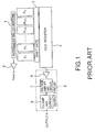
- FIG. 1 a plurality of photosensitive pixels for a picture are arranged in a matrix shape on a semiconductor substrate (not shown) so as to form a plurality of pixel trains P 1 through P n .
- a photosensitive pixel 1 for a monitor generates signal charges in proportion to a mean value of an incident light amount of the photosensitive pixels for a picture.
- the signal charges generated in the photosensitive pixel 1 for a monitor are outputted as a signal V AGC through an output buffer 2 so as to supply to a control circuit (not shown) externally provided.
- the control circuit opens a shift gate 3 at each time when the supplied signal V AGC reaches a predetermined threshold value, so as to transfer the signal charges to a charge coupled device (CCD) register 4.
- CCD charge coupled device
- Each of the signal charges transferred into the CCD register 4 are converted into an output signal in an output circuit 5 so as to be externally outputted.
- the output circuit 5 comprises an output buffer 6, a voltage amplifying circuit 7, and a clamp circuit 8.
- the voltage amplifying circuit 7 changes over a gain according to an instruction from the control circuit when the signal V AGC is less than the threshold value, for example, because an incident light amount is little. Furthermore, the clamp circuit 8 causes the output signal of the output circuit 5 to be within an input range of an analog/digital (A/D) converter provided in the latter stage, in which the lower and upper most values are set by the control circuit.
- A/D analog/digital
- the monitor photosensitive Pixel 1 is provided as means for measuring the mean value of the signal charges of each picture photosensitive pixel constituting the pixel trains P 1 -P n .
- the monitor photosensitive pixel 1 since the conventional CCD image sensor includes the output circuit 5 having the output signal of the output buffer 2 and the output signal V AGC which have different voltage gain and off-set voltage, the monitor photosensitive pixel 1 has a very bad accuracy as the measuring means for the mean value as described above.
- the CCD image sensor as shown in FIG. 1 also has the bad accuracy at the time when the threshold value is determined at opening the shift gate 3. Accordingly, such the CCD image sensor can not set the optimum threshold value corresponding to the incident light amount.
- US-A-4 809 077 discloses a solid state imaging device including a plurality of picture photosensitive pixels for generating first signal charges corresponding to an incident light amount, signal charge transfer means for transferring the first signal charges outputted from the picture photosensitive pixels, and a monitor photosensitive pixel for generating second signal charges, wherein an amplifying circuit for amplifying an output signal is controlled for setting a gain of the amplifying circuit.
- the solid state imaging device includes a plurality of picture photosensitive pixels for generating first signal charges corresponding to an incident light amount, signal charge transfer means for transferring in order the first signal charges outputted from the picture photosensitive pixels, and a monitor photosensitive pixels for generating second signal charges in proportion to the means value of the incident light amount of the picture photosensitive pixels having a predetermined number, in which the solid state imaging device comprises output means for converting both of the first and second signal charges into first and second output signals, in which the first signal charges are generated in the picture photosensitive pixels and transferred by the signal charge transfer means, and the second signal charges are generated in the monitor photosensitive pixels.
- the solid state imaging device is desired to further comprise a clamp circuit which is provided in the output means for clamping the output signal which is generated by converting the first signal charges transferred from the signal charge transfer means, and a control circuit for setting an upper limit or low limit voltage of the clamp circuit on the basis of the output signal which is generated by converting the second signal charges of the monitor photosensitive pixels by the output means.
- the solid state imaging device is desired to further comprise an amplifying circuit for amplifying the output signal which is converted from the first signal charges transferred from the signal charge transfer means, and a control circuit for setting a gain of the amplifying circuit on the basis of the output signal which is converted from the second signal charges outputted from the monitor photosensitive pixels.
- the optimum value can accurately be set with respect to the gain of the voltage amplifying circuit and the upper limit and low limit values of the clamp circuit by using the mean value.
- the solid state imaging device can accurately measure the mean value of the signal charges of the picture photosensitive pixels.
- FIG. 2 shows a block diagram schematically showing a constitution of a CCD image sensor according to a first embodiment of the present invention.
- a plurality of picture photosensitive pixels are arranged in a matrix shape on a semiconductor substrate (not shown), in which each line of the picture photosensitive pixels forms pixel trains P 1 -P n .
- signal charges. occurring in each picture photosensitive pixel can be transferred to the direction for a shift gate 12.
- Monitor photosensitive pixel 11 is arranged along two sides of a region in which the pixel trains P 1 -P n are arranged as shown in FIG. 2, so as to generate signal charges in proportion to a mean value of an incident light amount of these picture photosensitive pixels.
- a shift gate 12 comprises a portion which transfers the signal charges from the pixel trains P 1 -P n to the CCD register 13, and a portion which transfers the signal charges from the monitor photosensitive pixel 11. Opening and closing of the shift gate 12 are controlled by a control circuit 18 which will be mentioned later.
- the CCD register 13 takes into the signal charges occurring in the pixel trains P 1 -P n from the shift register 12 as a parallel signal so as to convert the parallel signal into a serial signal, thereby outputting the serial signal to an output circuit 14 which will be mentioned later.
- the signal charges occurring in the monitor photosensitive pixel 11 are taken by the shift gate 12, the signal charges are transferred to the output circuit 14 as they are.
- the output circuit 14 comprises an output buffer 15, a voltage amplifying circuit 16, and a clamping circuit 17, which are the same constitution as the conventional CCD image sensor.
- a control circuit 18 takes in order an output signal V AGC which is obtained by converting in the output circuit 14 the signal charges occurring in the monitor photosensitive pixel 11. At each time when an integral value of the signal V AGC reaches to a predetermined threshold value, any gate of the shift gate 12 is opened for transferring the signal charges occurring in the corresponding pixel in the picture photosensitive pixels P 1 -P n to the CCD register 13. Furthermore, the control circuit 18 changes over the gain in the voltage amplifying circuit 16 corresponding to a value of the signal V AGC . Moreover, the circuit 18 changes over the upper limit or low limit value of the clamping circuit 17 corresponding to the value of the signal V AGC .
- FIG. 3 is a graph showing a change with lapse of time of a voltage level in an output signal of the output circuit 14.
- the control circuit 18 opens a gate corresponding to the monitor photosensitive pixel 11 the shift gate 12.
- the signal charges occurring in the monitor photosensitive pixel 11 are transferred by the CCD register 13 into the output circuit 14 in which the signal charges are converted into the output signal V AGC .
- the signal V AGC is supplied to the control circuit 18 in which the value of the signal V AGC accurately corresponds to the mean value of the signal charges of the picture photosensitive pixels constituting the pixel trains P 1 -P n .
- the control circuit 18 uses the inputted signal V AGC and determines the threshold value for opening and closing the shift gate 12, the gain of the voltage amplifying circuit 18, and the upper limit and low limit values of the clamp in the clamping circuit 17 during a time T 1 .
- the gain of the voltage amplifying circuit 16 is controlled by comparing the signal V AGC with a plurality of judge levels (represented here as V 1 , V 2 , ...) in order.
- the gain may be set to the different values when V 1 > V AGC > V 2 , or when V 2 > V AGC > V 3 .
- the signal V AGC is clamped by the clamping circuit 17, it is possible to easily set the judge levels from the upper or low limit value of a clamping.
- the upper and low limit values of a clamp in the clamping circuit 17 are determined along the standard of the signal V AGC . Accordingly, since the value of the signal V AGC precisely corresponds to the mean value of the signal charges of the picture photosensitive pixels as has been described, it is unnecessary to determine the upper and low limit values of the clamp by using as the standard the signal charges which are generated in the shaded pixels. Therefore, in the first embodiment, since it is easy to set the optimum value with respect to the upper and low limit values, a high quality picture signal can be obtained even though there is a case where a contrast is small with respect to each signal charge in the picture photosensitive pixels.
- the threshold value for opening and closing the shift gate 12 is determined by an integral result of the signal V AGC supplied during the time T 1 .
- the control circuit 18 continuously inputs the signal V AGC and integrates the inputted signal V AGC .
- the circuit 18 closes the gate corresponding to the monitor photosensitive pixel 11 in the shift gate 12, and opens the gate corresponding to the picture photosensitive pixel trains P 1 -P n .
- the signal charges occurring in the picture photosensitive pixels are transferred to the CCD register 13 in which the charges are converted from a parallel signal into a serial signal so as to sequentially input into the output circuit 14.
- These signal charges are converted into voltage signals by an output buffer 15, which are amplified in the voltage amplifying circuit 16.
- the clamping circuit 17 clamps the amplified voltage signals so as to be outputted to an analog/digital converter (not shown) as the next stage.
- the single output circuit 14 converts the first signal charges occurring in the pixel trains P 1 -P n and the second signal charges occurring in the monitor photosensitive pixel 11 into the output signal to be outputted.
- the first embodiment to precisely set the optimum value with respect to the gain of the voltage amplifying circuit 16 and the upper and low limit values of the clamping circuit 17.
- the monitor photosensitive pixel is arranged along two sides of the region in which the pixels P 1 -P n are arranged.
- the present invention may comprise means for transferring the signal charges into the output circuit 14.
- the first embodiment comprises only one monitor photosensitive pixel
- another monitor photosensitive pixel and output buffer- may be provided in addition to the pixel 11 and output buffer 15.
- the CCD register 13 comprises an N-channel metal oxide semiconductor (MOS) transistor 131, and a capacitor 132, in which a signal V 1 is detected from a junction point between a drain of the transistor 131 and the capacitor 132. Furthermore, a control potential C 4 is detected from an electrode of the CCD register 13, and a control potential C 1 is supplied to a gate of the MOS transistor 131.
- MOS metal oxide semiconductor
- the output buffer 15 comprises an N-channel MOS transistor 151 having a gate to which the signal V 1 is supplied, and an N-MOS transistor 152 as a constant current source which is connected in series with the transistor 151. A potential of a junction point between the transistors 151 and 152 is stored in a capacitor 161 in the voltage amplifier circuit 16.
- the voltage amplifier circuit 16 comprises the capacitor 161, and N-MOS transistors 162-164, and has a characteristic in which an output operating point of the voltage amplifier circuit 16 is determined by a junction voltage V 20 between a drain-gate of the transistors 162 and 164 and the capacitor 161 and a junction potential V 2 between a source of the transistor 162 and a junction point of the transistors 163 and 164, as shown in FIG. 6.
- the control potential C 2 is supplied to a gate of the transistor 162.
- the clamping circuit 17 comprises a capacitor 171 and transistors 172-174, in which the capacitor 171 stores a junction potential V 2 of the voltage amplifier circuit 16.
- a control potential C 3 is supplied to a gate of the transistor 172, and a source of the transistor 172 is connected to a reference potential V ref .
- a potential of a junction point between the capacitor 171 and a drain of the transistor 172 is supplied to a gate of the transistor 173, and a potential V 3 of a junction point between a drain of the transistor 173 and a source of the transistor 174 as a constant current source is supplied to a control circuit 18 as the signal V AGC .
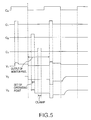
- a potential of each portion in FIG. 4 can be shown in a timing chart of FIG. 5, in which an output potential V 1 , V 2 and V 3 of the output buffer 15, voltage amplifying circuit 16 and clamping circuit 17 respectively have a wave form shown in FIG. 5.
- Control potentials C 1 -C 4 respective have timings shown in FIG. 5. In this manner, the mean value is clamped.
- FIG. 7 shows an output circuit 30 as a modified example of the output circuit 20 shown in FIG. 4.
- the output circuit 30 includes a voltage amplifying circuit 16A comprising transistors 165 and 169 both gates of which gains G 1 and G 2 are supplied in the manner that signal levels "H” and "L” are alternatively changed over, in the place of the voltage amplifying circuit 16 as shown in FIG. 4.
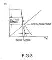
- FIG. 8 An output operating point of the voltage amplifying circuit 16A is shown in FIG. 8, and also a relationship between an output potential V' 2 and input potential V' 20 of the voltage amplifying circuit 16A is shown in FIG. 8.
- FIG. 9 shows a solid state imaging device according to a fourth embodiment, and is a modified example of the first embodiment shown in FIG. 2.
- a plurality of storage portions 40 and a plurality of charge drain portions 41 are provided between the picture photosensitive pixels P 1 -P n and shift gates 12.
- Each of the charge drain portions 41 comprises a gate 42 and a drain portion 43.
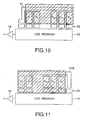
- FIGS. 10-13 show various modifications with respect to an arrangement between the picture photosensitive pixels P 1 -P n and the monitor photosensitive pixel 11.
- a solid state imaging device has the same constitution as the solid state imaging device according to the first embodiment.
- shift gates 12 are provided corresponding to the monitor photosensitive pixel 11 and the picture photosensitive pixels P 1 -P n , respectively.
- a region shown by an oblique line is a photosensitive pixel region. In this example, it is possible to clamp at a head of one line output.
- a solid state imaging device shows an example for clamping at the end of one line to the contrary with the solid state imaging according to the ninth embodiment. Accordingly, the monitor photosensitive pixel 11B is provided at a latter stage of the last picture photosensitive pixel P n .
- FIG. 12 shows a constitution of a solid state imaging device according to an seventh embodiment,
- a monitor photosensitive pixel 11C passes through second and third picture photosensitive pixels P 2 and P 3 , and opposes to the shift gate 12.
- the solid state imaging device according to the seventh embodiment is an example of changing over AGC/gain by an output of the monitor photosensitive pixel 11C.
- a clamp/operating point is set during a time interval W 1 by outputs of the shaded pixels P 1 and P 2 . Then, an AGC/gain are changed over by an output W 2 of the monitor photosensitive pixel. The judgement of the gain and the set of clamp/operating point are simultaneously performed during the time interval W 3 by an output of the shaded pixel P 3 .
Description
- The present invention relates to a solid state imaging device including a photosensitive pixel for monitoring, and applicable to an automatic focusing device for a camera and the like.
- A charge coupled device (CCD) image sensor has been well known as a solid state imaging device. There has been also well known a CCD image sensor including a photosensitive pixel for monitoring, which is applicable to the sensor used in an automatic focusing device of the camera and like, in order to control a storage time of a signal charge in each photosensitive pixel (for a picture) and a gain of an output circuit which converts the signal charge into an output signal.
- A solid state imaging device according to the preamble of
claim 1 is known from US-A-4 701 626. - A similar conventional device is described hereinbelow with reference to Fig. 1 of the drawings.
- In FIG. 1 a plurality of photosensitive pixels for a picture are arranged in a matrix shape on a semiconductor substrate (not shown) so as to form a plurality of pixel trains P1 through Pn. A
photosensitive pixel 1 for a monitor generates signal charges in proportion to a mean value of an incident light amount of the photosensitive pixels for a picture. - The signal charges generated in the
photosensitive pixel 1 for a monitor are outputted as a signal VAGC through anoutput buffer 2 so as to supply to a control circuit (not shown) externally provided. The control circuit opens a shift gate 3 at each time when the supplied signal VAGC reaches a predetermined threshold value, so as to transfer the signal charges to a charge coupled device (CCD)register 4. Each of the signal charges transferred into theCCD register 4 are converted into an output signal in anoutput circuit 5 so as to be externally outputted. Here, theoutput circuit 5 comprises anoutput buffer 6, a voltage amplifyingcircuit 7, and aclamp circuit 8. The voltage amplifyingcircuit 7 changes over a gain according to an instruction from the control circuit when the signal VAGC is less than the threshold value, for example, because an incident light amount is little. Furthermore, theclamp circuit 8 causes the output signal of theoutput circuit 5 to be within an input range of an analog/digital (A/D) converter provided in the latter stage, in which the lower and upper most values are set by the control circuit. - In this manner, in the CCD image sensor as shown in FIG. 1, the monitor
photosensitive Pixel 1 is provided as means for measuring the mean value of the signal charges of each picture photosensitive pixel constituting the pixel trains P1-Pn. - However, since the conventional CCD image sensor includes the
output circuit 5 having the output signal of theoutput buffer 2 and the output signal VAGC which have different voltage gain and off-set voltage, the monitorphotosensitive pixel 1 has a very bad accuracy as the measuring means for the mean value as described above. - Therefore, the CCD image sensor as shown in FIG. 1 also has the bad accuracy at the time when the threshold value is determined at opening the shift gate 3. Accordingly, such the CCD image sensor can not set the optimum threshold value corresponding to the incident light amount.
- Furthermore, since the accuracy of the output signal VAGC is wrong, it is impossible to set the optimum values of the gain of the voltage amplifying
circuit 7 and the upper and lower most values of theclamp circuit 8 by using the output signal VAGC. Therefore, it has been general to set the gain of the voltage amplifyingcircuit 7 and the upper and lower most values of theclamp circuit 8 to be the optimum value by using as a reference value the signal charges which are generated in a shaded, pixel provided at the head of the pixel trains P1-Pn and which is a signal pixel when the incident light amount is zero. - However, in the method of using the signal charges of such the shaded pixel, since the lowest level is used as the reference level without the mean level, it is impossible to sufficiently and accurately set the gain of the voltage amplifying
circuit 7 and the upper- and lower-most values of theclamp circuit 8. Such a fault becomes obvious according to the case where the contrast is small in the incident light amount of the pixel trains P1 to Pn. - From US-A-4 843 474 it is known to use common output means for converting first signal charges constituting image charges, and second signal charges constituting photometric or exposure charges, for converting both said first and second signal charges into first and second output signals.
- US-A-4 809 077 discloses a solid state imaging device including a plurality of picture photosensitive pixels for generating first signal charges corresponding to an incident light amount, signal charge transfer means for transferring the first signal charges outputted from the picture photosensitive pixels, and a monitor photosensitive pixel for generating second signal charges, wherein an amplifying circuit for amplifying an output signal is controlled for setting a gain of the amplifying circuit.
- It is an object of the present invention to provide a solid state imaging device according to the preamble of
claim 1 so as to improve the accuracy of the second signal charges in proportion to the mean value. - According to the present invention, this object is attainded by the features of the characterizing part of
claim 1. - Further improvements of the present invention are specified in the sub-claims.
- The solid state imaging device according to the present invention includes a plurality of picture photosensitive pixels for generating first signal charges corresponding to an incident light amount, signal charge transfer means for transferring in order the first signal charges outputted from the picture photosensitive pixels, and a monitor photosensitive pixels for generating second signal charges in proportion to the means value of the incident light amount of the picture photosensitive pixels having a predetermined number, in which the solid state imaging device comprises output means for converting both of the first and second signal charges into first and second output signals, in which the first signal charges are generated in the picture photosensitive pixels and transferred by the signal charge transfer means, and the second signal charges are generated in the monitor photosensitive pixels.
- As an aspect of the present invention, the solid state imaging device is desired to further comprise a clamp circuit which is provided in the output means for clamping the output signal which is generated by converting the first signal charges transferred from the signal charge transfer means, and a control circuit for setting an upper limit or low limit voltage of the clamp circuit on the basis of the output signal which is generated by converting the second signal charges of the monitor photosensitive pixels by the output means.
- As a second aspect of the present invention, the solid state imaging device is desired to further comprise an amplifying circuit for amplifying the output signal which is converted from the first signal charges transferred from the signal charge transfer means, and a control circuit for setting a gain of the amplifying circuit on the basis of the output signal which is converted from the second signal charges outputted from the monitor photosensitive pixels.
- By the above construction, since the voltage gain and the off-set voltage of the first and second signal charges are caused to be equal to each other by the same output means which outputs the first signal charges generated in the picture photosensitive pixels and the second signal charges generated in the monitor photosensitive pixels, it is possible to accurately measure the means value of the first signal charges of the picture photosensitive pixels.
- Furthermore, since it is possible to accurately measure the mean value of the first signal charges of the picture photosensitive pixels in the above way, the optimum value can accurately be set with respect to the gain of the voltage amplifying circuit and the upper limit and low limit values of the clamp circuit by using the mean value.
- As described above, the solid state imaging device according to the present invention can accurately measure the mean value of the signal charges of the picture photosensitive pixels.
- Accordingly, it is possible to precisely set the optimum value with respect to the gain of the voltage amplifying circuit and the upper limit and low limit values of the clamp circuit both provided in the output circuit.
- In the accompanying drawings:
- FIG. 1 is a block diagram schematically showing a constitution of the conventional solid state imaging device;
- FIG. 2 is a block diagram schematically showing a constitution of a solid state imaging device according to a first embodiment of the present invention;
- FIG. 3 is a graph showing a change with lapse of time in a output signal of an output circuit shown in FIG. 2;
- FIG. 4 is a circuit diagram showing an output circuit according to a second embodiment of the present invention as a detailed circuitry of the output circuit of the solid state imaging device according to the first embodiment;
- FIG. 5 is graph showing a change of the output signals of the output circuit shown in FIG. 4;
- FIG. 6 is a graph showing an input/output relationship for explaining an operating point of an output buffer in the output circuit shown in FIG. 4;
- FIG. 7 is a circuit diagram showing an output circuit according to a third embodiment of the present invention including a different and detailed constitution;
- FIG. 8 is a graph showing an input/output relationship for explaining an operating point of an output buffer in the output ci'rcuit shown in FIG.7;
- FIG. 9 is a block diagram showing a solid state imaging device according to a fourth embodiment of the present invention;
- FIG. 10 is a block diagram showing a solid state imaging device according to a fifth embodiment of the present invention;
- FIG. 11 is a block diagram showing a solid state imaging device according to a sixth embodiment of the present invention;
- FIG. 12 is a circuit diagram showing a solid state imaging device according to a seventh embodiment of the present invention;
- FIG. 13 is a graph showing a change with lapse of time in an output signal of an output circuit shown in FIG. 12.
-
- There will be described in detail a solid state imaging device by using a CCD image sensor as an example according to preferred embodiments of the present invention in reference with the attached drawings.
- FIG. 2 shows a block diagram schematically showing a constitution of a CCD image sensor according to a first embodiment of the present invention.
- In FIG. 2, a plurality of picture photosensitive pixels are arranged in a matrix shape on a semiconductor substrate (not shown), in which each line of the picture photosensitive pixels forms pixel trains P1-Pn. Here, signal charges. occurring in each picture photosensitive pixel can be transferred to the direction for a
shift gate 12. - Monitor
photosensitive pixel 11 is arranged along two sides of a region in which the pixel trains P1-Pn are arranged as shown in FIG. 2, so as to generate signal charges in proportion to a mean value of an incident light amount of these picture photosensitive pixels. - A
shift gate 12 comprises a portion which transfers the signal charges from the pixel trains P1-Pn to theCCD register 13, and a portion which transfers the signal charges from the monitorphotosensitive pixel 11. Opening and closing of theshift gate 12 are controlled by acontrol circuit 18 which will be mentioned later. - The
CCD register 13 takes into the signal charges occurring in the pixel trains P1-Pn from theshift register 12 as a parallel signal so as to convert the parallel signal into a serial signal, thereby outputting the serial signal to anoutput circuit 14 which will be mentioned later. When the signal charges occurring in the monitorphotosensitive pixel 11 are taken by theshift gate 12, the signal charges are transferred to theoutput circuit 14 as they are. - The
output circuit 14 comprises anoutput buffer 15, a voltage amplifyingcircuit 16, and aclamping circuit 17, which are the same constitution as the conventional CCD image sensor. - A
control circuit 18 takes in order an output signal VAGC which is obtained by converting in theoutput circuit 14 the signal charges occurring in the monitorphotosensitive pixel 11. At each time when an integral value of the signal VAGC reaches to a predetermined threshold value, any gate of theshift gate 12 is opened for transferring the signal charges occurring in the corresponding pixel in the picture photosensitive pixels P1-Pn to theCCD register 13. Furthermore, thecontrol circuit 18 changes over the gain in thevoltage amplifying circuit 16 corresponding to a value of the signal VAGC. Moreover, thecircuit 18 changes over the upper limit or low limit value of theclamping circuit 17 corresponding to the value of the signal VAGC. - Next, there will be described operation of the CCD image sensor shown in FIG. 2 in accordance with FIG. 3 which is a graph showing a change with lapse of time of a voltage level in an output signal of the
output circuit 14. - First, the
control circuit 18 opens a gate corresponding to the monitorphotosensitive pixel 11 theshift gate 12. By this, the signal charges occurring in the monitorphotosensitive pixel 11 are transferred by theCCD register 13 into theoutput circuit 14 in which the signal charges are converted into the output signal VAGC. The signal VAGC is supplied to thecontrol circuit 18 in which the value of the signal VAGC accurately corresponds to the mean value of the signal charges of the picture photosensitive pixels constituting the pixel trains P1-Pn. - The
control circuit 18 uses the inputted signal VAGC and determines the threshold value for opening and closing theshift gate 12, the gain of thevoltage amplifying circuit 18, and the upper limit and low limit values of the clamp in theclamping circuit 17 during a time T1. - Here, the gain of the
voltage amplifying circuit 16 is controlled by comparing the signal VAGC with a plurality of judge levels (represented here as V1, V2, ...) in order. For example, the gain may be set to the different values when V1 > VAGC > V2, or when V2 > VAGC > V3. In the first embodiment, since the signal VAGC is clamped by the clampingcircuit 17, it is possible to easily set the judge levels from the upper or low limit value of a clamping. - Furthermore, the upper and low limit values of a clamp in the
clamping circuit 17 are determined along the standard of the signal VAGC. Accordingly, since the value of the signal VAGC precisely corresponds to the mean value of the signal charges of the picture photosensitive pixels as has been described, it is unnecessary to determine the upper and low limit values of the clamp by using as the standard the signal charges which are generated in the shaded pixels. Therefore, in the first embodiment, since it is easy to set the optimum value with respect to the upper and low limit values, a high quality picture signal can be obtained even though there is a case where a contrast is small with respect to each signal charge in the picture photosensitive pixels. - Furthermore, the threshold value for opening and closing the
shift gate 12 is determined by an integral result of the signal VAGC supplied during the time T1. - When the threshold value is determined, the
control circuit 18 continuously inputs the signal VAGC and integrates the inputted signal VAGC. When the integral result reaches to the threshold value, thecircuit 18 closes the gate corresponding to the monitorphotosensitive pixel 11 in theshift gate 12, and opens the gate corresponding to the picture photosensitive pixel trains P1-Pn. By this, the signal charges occurring in the picture photosensitive pixels are transferred to theCCD register 13 in which the charges are converted from a parallel signal into a serial signal so as to sequentially input into theoutput circuit 14. These signal charges are converted into voltage signals by anoutput buffer 15, which are amplified in thevoltage amplifying circuit 16. The clampingcircuit 17 clamps the amplified voltage signals so as to be outputted to an analog/digital converter (not shown) as the next stage. - In this manner, in the CCD image sensor according to the first embodiment, the
single output circuit 14 converts the first signal charges occurring in the pixel trains P1-Pn and the second signal charges occurring in the monitorphotosensitive pixel 11 into the output signal to be outputted.' Accordingly, since the voltage gain and the off-set are the same in these signal charges, it is possible to improve the accuracy of the mean value of the signal charges of the picture photosensitive pixels measured by the monitorphotosensitive pixel 11. - Therefore, it is possible for the first embodiment to precisely set the optimum value with respect to the gain of the
voltage amplifying circuit 16 and the upper and low limit values of the clampingcircuit 17. - In the first embodiment the monitor photosensitive pixel is arranged along two sides of the region in which the pixels P1-Pn are arranged.
- Furthermore, even though the first embodiment adopts the configuration in which the
shift register 12 and theCCD register 13 transfer the signal charges occurring in the monitorphotosensitive pixel 11 into theoutput circuit 14, the present invention may comprise means for transferring the signal charges into theoutput circuit 14. - Moreover, even though the first embodiment comprises only one monitor photosensitive pixel, another monitor photosensitive pixel and output buffer-may be provided in addition to the
pixel 11 andoutput buffer 15. - In the solid state imaging device according to the first embodiment shown in FIG. 2, if the
output circuit 14 is described in detail, there is an output circuit 20 according to a second embodiment shown in FIG. 4. - In FIG. 4, components attached by the same numerals in FIG. 2 are the same components in the solid state imaging device according to the first embodiment. The
CCD register 13 comprises an N-channel metal oxide semiconductor (MOS)transistor 131, and acapacitor 132, in which a signal V1 is detected from a junction point between a drain of thetransistor 131 and thecapacitor 132. Furthermore, a control potential C4 is detected from an electrode of theCCD register 13, and a control potential C1 is supplied to a gate of theMOS transistor 131. - The
output buffer 15 comprises an N-channel MOS transistor 151 having a gate to which the signal V1 is supplied, and an N-MOS transistor 152 as a constant current source which is connected in series with the transistor 151. A potential of a junction point between the transistors 151 and 152 is stored in a capacitor 161 in thevoltage amplifier circuit 16. - The
voltage amplifier circuit 16 comprises the capacitor 161, and N-MOS transistors 162-164, and has a characteristic in which an output operating point of thevoltage amplifier circuit 16 is determined by a junction voltage V20 between a drain-gate of thetransistors transistor 162 and a junction point of thetransistors transistor 162. - The clamping
circuit 17 comprises acapacitor 171 and transistors 172-174, in which thecapacitor 171 stores a junction potential V2 of thevoltage amplifier circuit 16. A control potential C3 is supplied to a gate of thetransistor 172, and a source of thetransistor 172 is connected to a reference potential Vref. A potential of a junction point between thecapacitor 171 and a drain of thetransistor 172 is supplied to a gate of the transistor 173, and a potential V3 of a junction point between a drain of the transistor 173 and a source of the transistor 174 as a constant current source is supplied to acontrol circuit 18 as the signal VAGC. - A potential of each portion in FIG. 4 can be shown in a timing chart of FIG. 5, in which an output potential V1, V2 and V3 of the
output buffer 15,voltage amplifying circuit 16 and clampingcircuit 17 respectively have a wave form shown in FIG. 5. Control potentials C1-C4 respective have timings shown in FIG. 5. In this manner, the mean value is clamped. - Next, using FIGS. 7 and 8, there is described a solid state imaging device according to a third embodiment of the present invention. FIG. 7 shows an
output circuit 30 as a modified example of the output circuit 20 shown in FIG. 4. Theoutput circuit 30 includes avoltage amplifying circuit 16A comprising transistors voltage amplifying circuit 16 as shown in FIG. 4. - An output operating point of the
voltage amplifying circuit 16A is shown in FIG. 8, and also a relationship between an output potential V'2 and input potential V'20 of thevoltage amplifying circuit 16A is shown in FIG. 8. - FIG. 9 shows a solid state imaging device according to a fourth embodiment, and is a modified example of the first embodiment shown in FIG. 2. In FIG. 9, a plurality of storage portions 40 and a plurality of
charge drain portions 41 are provided between the picture photosensitive pixels P1-Pn and shiftgates 12. Each of thecharge drain portions 41 comprises agate 42 and adrain portion 43. By the constitution, even though an idling current occurs in the same manner of other pixels in the monitor photosensitive pixel, the idling current is compensated by the storage portions 40 and thecharge drain portions 41. - FIGS. 10-13 show various modifications with respect to an arrangement between the picture photosensitive pixels P1-Pn and the monitor
photosensitive pixel 11. - A solid state imaging device according to a fifth embodiment shown in FIG. 10 has the same constitution as the solid state imaging device according to the first embodiment. In FIG. 10,
shift gates 12 are provided corresponding to the monitorphotosensitive pixel 11 and the picture photosensitive pixels P1-Pn, respectively. In the figure, a region shown by an oblique line is a photosensitive pixel region. In this example, it is possible to clamp at a head of one line output. - A solid state imaging device according to a sixth embodiment shown in FIG. 11 shows an example for clamping at the end of one line to the contrary with the solid state imaging according to the ninth embodiment. Accordingly, the monitor
photosensitive pixel 11B is provided at a latter stage of the last picture photosensitive pixel Pn. - FIG. 12 shows a constitution of a solid state imaging device according to an seventh embodiment, In the figure, a monitor
photosensitive pixel 11C passes through second and third picture photosensitive pixels P2 and P3, and opposes to theshift gate 12. The solid state imaging device according to the seventh embodiment is an example of changing over AGC/gain by an output of the monitorphotosensitive pixel 11C. - In FIG. 13 for explaining operation of the seventh embodiment, a clamp/operating point is set during a time interval W1 by outputs of the shaded pixels P1 and P2. Then, an AGC/gain are changed over by an output W2 of the monitor photosensitive pixel. The judgement of the gain and the set of clamp/operating point are simultaneously performed during the time interval W3 by an output of the shaded pixel P3.
Claims (4)
- A solid state imaging device including a plurality of picture photosensitive pixels (P1-Pn) for generating first signal charges corresponding to an incident light amount;characterized bysignal charge transfer means (13) for transferring in the order the first signal charges outputted from the picture photosensitive pixels (P1-Pn); anda monitor photosensitive pixel (11; 11B; 11C) for generating second signal charges in proportion to a mean value of the amount of light incident on the picture photosensitive pixels (P1-Pn);common output means (14) for converting both said first and second signal charges into first and second output signals, in which the first signal charges are generated in the picture photosensitive pixels (P1-Pn) and transferred by the signal charge transfer means (13), and the second signal charges are generated in the monitor photosensitive pixel (11; 11B; 11C) and transferred by the signal charge transfer means (13); anda common signal charge path including a CCD register and provided between said common output means (14) and said picture photosensitive pixels (P1-Pn) and said monitor photosensitive pixel (11; 11B; 11C);wherein said monitor photosensitive pixel (11; 11B; 11C) has a predetermined area extending along two sides of a region in which said picture photosensitive pixels (P1-Pn) are arranged so as to generate signal charges in proportion to said mean value of the amount of light incident on said picture photosensitive pixels (P1-Pn).
- The solid state imaging device according to claim 1, characterized bya clamping circuit (17) provided in the output means (14) for clamping the output signal which is generated by converting the first signal charges transferred from the signal charge transfer means (13); anda control circuit (18) for setting an upper limit or low limit voltage of the clamping circuit (17) on the basis of the output signal which is generated by said output means (14) by converting the second signal charges of the monitor phototsensitive pixel (11; 11B; 11C).
- The solid state imaging device according to claim 1 or 2, characterized byan amplifying circuit (16) for amplifying the output signal which is converted from the first signal charges transferred from the signal charge transfer means (13); anda control circuit (18) for setting a gain of the amplifying circuit (16) on the basis of the output signal which is converted from the second signal charges outputted from the monitor photosensitive pixel (11; 11B; 11C).
- The solid state imaging device according to any of claims 1 to 3, characterized in said that another monitor phototsensitive pixel and output buffer are provided in addition to said monitor photosensitive pixel (11; 11B; 11C) and output buffer (15).
Applications Claiming Priority (3)
| Application Number | Priority Date | Filing Date | Title |
|---|---|---|---|
| JP331562/93 | 1993-12-27 | ||
| JP33156293 | 1993-12-27 | ||
| JP33156293 | 1993-12-27 |
Publications (2)
| Publication Number | Publication Date |
|---|---|
| EP0660598A1 EP0660598A1 (en) | 1995-06-28 |
| EP0660598B1 true EP0660598B1 (en) | 1999-07-28 |
Family
ID=18245051
Family Applications (1)
| Application Number | Title | Priority Date | Filing Date |
|---|---|---|---|
| EP94120669A Expired - Lifetime EP0660598B1 (en) | 1993-12-27 | 1994-12-27 | Solid state imaging device including monitoring pixel |
Country Status (4)
| Country | Link |
|---|---|
| US (1) | US5606367A (en) |
| EP (1) | EP0660598B1 (en) |
| KR (1) | KR100196818B1 (en) |
| DE (1) | DE69419704T2 (en) |
Families Citing this family (5)
| Publication number | Priority date | Publication date | Assignee | Title |
|---|---|---|---|---|
| US6469289B1 (en) * | 2000-01-21 | 2002-10-22 | Symagery Microsystems Inc. | Ambient light detection technique for an imaging array |
| CA2330433A1 (en) * | 2000-01-21 | 2001-07-21 | Symagery Microsystems Inc. | Smart exposure determination for imagers |
| JP2002044421A (en) * | 2000-07-28 | 2002-02-08 | Ricoh Co Ltd | Image reader and its control method and image processor |
| GB0020857D0 (en) | 2000-08-25 | 2000-10-11 | Vlsi Vision Ltd | Method of detecting flicker and video camera using the method |
| RU2699805C1 (en) * | 2018-10-08 | 2019-09-11 | Вячеслав Михайлович Смелков | Method of controlling sensitivity of a television camera on a ccd matrix and reproducing its video signal in a mobile device in conditions of high illumination and/or complex brightness of objects |
Family Cites Families (13)
| Publication number | Priority date | Publication date | Assignee | Title |
|---|---|---|---|---|
| JPS5795771A (en) * | 1980-12-05 | 1982-06-14 | Fuji Photo Film Co Ltd | Solid-state image pickup device |
| US4635126A (en) * | 1981-12-18 | 1987-01-06 | Canon Kabushiki Kaisha | Image pick-up system |
| JP2514314B2 (en) * | 1983-04-22 | 1996-07-10 | 旭光学工業株式会社 | Method and apparatus for controlling storage time of storage photoelectric converter |
| JPS6058780A (en) * | 1983-09-09 | 1985-04-04 | Olympus Optical Co Ltd | Solid-state image pickup device provided with photometric function |
| JPS6074878A (en) * | 1983-09-30 | 1985-04-27 | Canon Inc | Store time corrector of photoelectric transducer |
| JPS62230269A (en) * | 1986-03-31 | 1987-10-08 | Toshiba Corp | Electronic still picture camera |
| JP2623530B2 (en) * | 1986-04-22 | 1997-06-25 | ミノルタ株式会社 | Solid-state image sensor drive |
| JPH07114474B2 (en) * | 1987-01-05 | 1995-12-06 | 株式会社東芝 | Electronic still camera |
| US5162913A (en) * | 1990-02-26 | 1992-11-10 | Medical Concepts, Inc. | Apparatus for modulating the output of a ccd camera |
| JP3086696B2 (en) * | 1990-08-24 | 2000-09-11 | 株式会社東芝 | Image signal processing device |
| US5267015A (en) * | 1990-10-09 | 1993-11-30 | Nikon Corporation | Photometric apparatus |
| JP3061410B2 (en) * | 1990-11-15 | 2000-07-10 | ソニー株式会社 | Solid-state imaging device |
| JP3100762B2 (en) * | 1992-06-11 | 2000-10-23 | 株式会社東芝 | Clamp circuit for digital camera |
-
1994
- 1994-12-23 KR KR1019940036227A patent/KR100196818B1/en not_active IP Right Cessation
- 1994-12-27 DE DE69419704T patent/DE69419704T2/en not_active Expired - Lifetime
- 1994-12-27 US US08/364,326 patent/US5606367A/en not_active Expired - Lifetime
- 1994-12-27 EP EP94120669A patent/EP0660598B1/en not_active Expired - Lifetime
Also Published As
| Publication number | Publication date |
|---|---|
| DE69419704T2 (en) | 1999-12-16 |
| DE69419704D1 (en) | 1999-09-02 |
| KR950021702A (en) | 1995-07-26 |
| KR100196818B1 (en) | 1999-06-15 |
| EP0660598A1 (en) | 1995-06-28 |
| US5606367A (en) | 1997-02-25 |
Similar Documents
| Publication | Publication Date | Title |
|---|---|---|
| EP0458030B1 (en) | Defect correction for CCD and CID imagers | |
| US20060119717A1 (en) | Asymmetric comparator for use in pixel oversaturation detection | |
| EP0700195A2 (en) | Method of calibration of image scanner signal processing circuits | |
| US5216511A (en) | Imaging device with elimination of dark current | |
| US7623171B2 (en) | Multiple crawbar switching in charge domain linear operations | |
| US5008698A (en) | Control apparatus for image sensor | |
| JPS6135684A (en) | Solid-state image pickup device | |
| US6881944B2 (en) | Solid state image sensor with signal line potential adjustment circuit and method of driving the same | |
| US4620236A (en) | Image picture reading device | |
| EP0660598B1 (en) | Solid state imaging device including monitoring pixel | |
| JPH05502309A (en) | Autofocus chip with reference level setting circuit | |
| US8948584B2 (en) | Photoelectric conversion device and camera system | |
| US6201617B1 (en) | Image sensing device | |
| US7295237B2 (en) | Image capturing apparatus capable of extracting a moving object | |
| US6466267B1 (en) | System for performing selective detection of image signal peaks and camera employing the system | |
| KR100213958B1 (en) | Image signal processing apparatus | |
| US6867409B2 (en) | Solid-state image sensing device | |
| JP2770795B2 (en) | Calibration method and device for multi-element sensor | |
| JPH06311441A (en) | Solid-state image pickup device | |
| JP3310123B2 (en) | Solid-state imaging device | |
| US6259087B1 (en) | Calibration apparatus for multi-element sensor | |
| JPH07327174A (en) | Solid-state image pickup device | |
| JP2008028634A (en) | Imaging apparatus | |
| JPH05122614A (en) | Image pickup device | |
| JP3021943B2 (en) | Color television camera device |
Legal Events
| Date | Code | Title | Description |
|---|---|---|---|
| PUAI | Public reference made under article 153(3) epc to a published international application that has entered the european phase |
Free format text: ORIGINAL CODE: 0009012 |
|
| 17P | Request for examination filed |
Effective date: 19941227 |
|
| AK | Designated contracting states |
Kind code of ref document: A1 Designated state(s): DE FR GB |
|
| 17Q | First examination report despatched |
Effective date: 19951117 |
|
| GRAG | Despatch of communication of intention to grant |
Free format text: ORIGINAL CODE: EPIDOS AGRA |
|
| GRAG | Despatch of communication of intention to grant |
Free format text: ORIGINAL CODE: EPIDOS AGRA |
|
| GRAH | Despatch of communication of intention to grant a patent |
Free format text: ORIGINAL CODE: EPIDOS IGRA |
|
| GRAH | Despatch of communication of intention to grant a patent |
Free format text: ORIGINAL CODE: EPIDOS IGRA |
|
| GRAA | (expected) grant |
Free format text: ORIGINAL CODE: 0009210 |
|
| AK | Designated contracting states |
Kind code of ref document: B1 Designated state(s): DE FR GB |
|
| REF | Corresponds to: |
Ref document number: 69419704 Country of ref document: DE Date of ref document: 19990902 |
|
| ET | Fr: translation filed | ||
| PG25 | Lapsed in a contracting state [announced via postgrant information from national office to epo] |
Ref country code: GB Free format text: LAPSE BECAUSE OF NON-PAYMENT OF DUE FEES Effective date: 19991227 |
|
| PLBE | No opposition filed within time limit |
Free format text: ORIGINAL CODE: 0009261 |
|
| STAA | Information on the status of an ep patent application or granted ep patent |
Free format text: STATUS: NO OPPOSITION FILED WITHIN TIME LIMIT |
|
| 26N | No opposition filed | ||
| GBPC | Gb: european patent ceased through non-payment of renewal fee |
Effective date: 19991227 |
|
| PGFP | Annual fee paid to national office [announced via postgrant information from national office to epo] |
Ref country code: DE Payment date: 20131224 Year of fee payment: 20 |
|
| PGFP | Annual fee paid to national office [announced via postgrant information from national office to epo] |
Ref country code: FR Payment date: 20131209 Year of fee payment: 20 |
|
| REG | Reference to a national code |
Ref country code: DE Ref legal event code: R071 Ref document number: 69419704 Country of ref document: DE |
|
| REG | Reference to a national code |
Ref country code: DE Ref legal event code: R071 Ref document number: 69419704 Country of ref document: DE |