EP0663638B1 - A method of configuring computer peripherals - Google Patents
A method of configuring computer peripherals Download PDFInfo
- Publication number
- EP0663638B1 EP0663638B1 EP94309649A EP94309649A EP0663638B1 EP 0663638 B1 EP0663638 B1 EP 0663638B1 EP 94309649 A EP94309649 A EP 94309649A EP 94309649 A EP94309649 A EP 94309649A EP 0663638 B1 EP0663638 B1 EP 0663638B1
- Authority
- EP
- European Patent Office
- Prior art keywords
- peripheral adapter
- user
- operating parameters
- options
- configuration
- Prior art date
- Legal status (The legal status is an assumption and is not a legal conclusion. Google has not performed a legal analysis and makes no representation as to the accuracy of the status listed.)
- Expired - Lifetime
Links
Images


Classifications
-
- G—PHYSICS
- G06—COMPUTING; CALCULATING OR COUNTING
- G06F—ELECTRIC DIGITAL DATA PROCESSING
- G06F9/00—Arrangements for program control, e.g. control units
- G06F9/06—Arrangements for program control, e.g. control units using stored programs, i.e. using an internal store of processing equipment to receive or retain programs
- G06F9/44—Arrangements for executing specific programs
- G06F9/4401—Bootstrapping
- G06F9/4411—Configuring for operating with peripheral devices; Loading of device drivers
-
- G—PHYSICS
- G06—COMPUTING; CALCULATING OR COUNTING
- G06F—ELECTRIC DIGITAL DATA PROCESSING
- G06F13/00—Interconnection of, or transfer of information or other signals between, memories, input/output devices or central processing units
- G06F13/38—Information transfer, e.g. on bus
- G06F13/382—Information transfer, e.g. on bus using universal interface adapter
- G06F13/385—Information transfer, e.g. on bus using universal interface adapter for adaptation of a particular data processing system to different peripheral devices
-
- G—PHYSICS
- G06—COMPUTING; CALCULATING OR COUNTING
- G06F—ELECTRIC DIGITAL DATA PROCESSING
- G06F15/00—Digital computers in general; Data processing equipment in general
- G06F15/16—Combinations of two or more digital computers each having at least an arithmetic unit, a program unit and a register, e.g. for a simultaneous processing of several programs
- G06F15/177—Initialisation or configuration control
Definitions
- one of the Reserved registers (at 28 16 , 2C 16 , 34 16 or 38 16 ) in the header region 36 will include the PCF_Required field, preferably as a single bit field.
- a value of "1" in the PCF_Required field will indicate that user selection of one or more configuration options is supported.
- a value of "0" in the PCF_Required field will indicate that the peripheral adapter does not require user selection of any configuration options.
- the next clock edge begins the first of one or more data phases, during which data is transferred by the AD signals between the processor and the peripheral adapter on each clock edge for which both the IRDY# and TRDY# signals are asserted by the processor and the peripheral adapter, respectively. Wait cycles may be inserted in the data phases by either the processor or the peripheral adapter by deasserting the IRDY# and TRDY# signals, respectively.
- the processor intends to complete only one more data transfer (which could be immediately after the address phase)
- the FRAME# signal is de-asserted and the IRDY# signal is asserted indicating the processor is ready.
- the peripheral adapter indicates the final data transfer, by asserting the TRDY# signal, the PCI bus returns to the idle state with both the FRAME# and IRDY# signals de-asserted.
- the VENDOR and DEVICE keywords must match the equivalent fields in the Configuration Space of the peripheral adapter.
- the PCFDEF parameter indicates the version of the syntax specification.
- the ENDPCF keyword specifies the end of the PCF. Any information that follows the ENDPCF keyword will not be parsed. ;
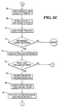
- FIGS. 5A-5G together are a flowchart illustrating the steps performed by the present invention.
- block 54 represents the processor accessing the Code Type field in the PCI Data Structure 44 of the first image region of the Expansion ROM 40.
- Decision block 56 represents the processor determining whether the Code Type field contains a "PCF" value. If not, control transfers to block 58.
- Block 58 is a decision block that determines whether there are additional image regions in the Expansion ROM 40. If not, control transfers to "A”. Otherwise, control transfers to block 54 to access the Code Type field in the PCI Data Structure 44 of the next image region of the Expansion ROM 40. If the processor determines at block 56 that the Code Type field contains a "PCF" value, then block 60 represents the processor retrieving the PCF from the device dependent region 46 of the Expansion ROM 40. Control then transfers to "B".
Description
- This invention relates in general to methods of configuring computer systems, and in particular to a method of configuring a peripheral adapter.
- The peripheral component interface (PCI) Local Bus Specification, Production Version, Revision 2.0, dated April 30, 1993 defines the standard mechanism to support the connection of peripheral devices to a PCI local bus. The PCI Specification also addresses how peripheral devices can define system resource requirements and communicate those requirements to the computer. It is recognized that some devices will require user selection of configuration options. The PCI Specification does not, however, address how a peripheral device conveys device-specific configuration options to a system utility such that they can be presented to a user for selection and to the computer for configuring the peripheral device.
- Without a standard mechanism for configuring peripheral devices, each vendor would provide their own unique configuration mechanism. For PCI systems that already support a system configuration utility, for example, where the PCI system includes a MicroChannel™ (MCA) or EISA bus and uses the MCA or EISA configuration utilities, it would be unacceptable to require users to use multiple configuration utilities, i.e., one for each of the peripheral devices. Moreover, vendors would be forced to deal with the development and management headaches associated with multiple configuration utilities for multiple operating environments.
- It is an object of the present invention to provide a method of configuring computer peripherals which overcomes the problems discussed above.
- According to the present invention there is provided a method of configuring a peripheral adapter coupled to a computer, comprising the steps of: (a): (a) determining if said peripheral adapter has user-selectable operating parameters; (b) accessing a configuration file stored in the peripheral adapter when said peripheral adapter has user-selectable operating parameters; (c) interpreting the configuration file's contents to identify options for the user-selectable operating parameters of said peripheral adapter; (d) presenting the options for the user-selectable operating parameters of said peripheral adapter to an operator; (e) accepting a selection of one of the options for each of the user-selectable operating parameters of said peripheral adapter from the operator; and (f) setting the operating parameters of said peripheral adapter according to the selected option.
- An embodiment of the present invention will now be described, by way of example, with reference to the accompanying drawings in which:
- Fig. 1 is a block diagram of an example configuration using the PCl bus;
- Fig. 2 is a block diagram illustrating the format of the Configuration Space in a PCI adapter;
- Fig. 3 is a block diagram illustrating the format of the Expansion ROM in a PCI adapter;
- Fig. 4 is a timing chart illustrating a Configuration Read transaction between the processor and the PCI adapter; and
- Figs. 5A-5G together are a flowchart illustrating the steps performed by a configuration utility program executed by the processor.
-
- Figure 1 is a block diagram of an example configuration using a Peripheral Component Interconnect (PCI)
bus 10. ThePCI bus 10 is a physical interconnect apparatus intended for use between peripheral devices or adapters and processor/memory systems. ThePCI bus 10 is intended as a standard interface at the component level in much the same way that ISA, EISA, or MCA buses are standard interfaces at the board level. Just as ISA, EISA, and MCA buses provide a common I/O board interface across different platforms and different processor generations, thePCI bus 10 is intended to be a common I/O component interface across different platforms and different processor generations. A more complete discussion of thePCI bus 10 is available in the document PCI Local Bus Specification, Production Version, Revision 2.0, April 30, 1993. - In Figure 1, a processor/
memory subsystem 12 is coupled to thePCI bus 10, as are such peripheral adapters asaudio boards 14,video boards 16,video graphics controllers 18 formonitors 20,SCSI peripherals 22,LAN interfaces 24, and otherperipheral devices 26.Bridge interface logic 28 couples thePCI bus 10 to astandard expansion bus 30 and provides access therebetween for various expansion I/O boards 32. Those skilled in the art will recognize that this example configuration is not intended to imply any specific architectural limits. - As described in more detail below, the present invention proposes a configuration method for peripheral adapters coupled to the
PCI bus 10. The peripheral adapters have user-selectable, device-specific configuration options, wherein the options are defined by a PCI Configuration File (PCF) supplied with the peripheral adapter. Initially, the processor accesses a PCF_Required flag in a Configuration Space in the targeted peripheral adapter. If the PCF_Required flag is set, then the processor accesses an Expansion ROM in the peripheral adapter to determine whether the PCF resides in the Expansion ROM. If not found in the Expansion ROM, then the processor examines other non-volatile storage or the operator is prompted to supply a diskette containing the PCF. Once the PCF has been retrieved by the processor, the keywords therein are interpreted to prompt the user for selections among the different configuration options. Once the user selections have been made, the processor updates the appropriate registers in the Configuration Space of the peripheral adapter with the user-selected values and stores the user selections in non-volatile storage for the next boot or cold-start of the system. - The method of the present invention offers a number of advantages over the prior art. One advantage is that the present invention allows users to specify requirements or preferences for peripheral devices. Further, the present invention is both operating system and system architecture independent. The configuration files are formatted using ANSI, ASCII, EBCDIC, or ISO 8859.1 text, so that they are not restricted to any particular platform. Moreover, the syntax specification of the configuration files is extensible, so that revisions can be easily introduced while maintaining backward compatibility with prior versions.
- Another advantage is that the syntax specification provides a generic capability to convey device-specific information. The syntax specification is simple and consists of only a few keywords, so that a vendor can use generic text strings to describe configuration registers, functions, features, and options. This eliminates the need for a large and complex keyword list to handle all possible configuration options.
- Still another advantage is that the present invention has only a minimal effect on the PCI Specification, even though it comprises an extension beyond the PCI Specification. The present invention needs only a single bit in the PCI-defined Configuration Space to identify those devices that support user selection of configuration options. Moreover, the use of this single bit does not adversely affect peripheral adapters that are not configurable, because the bit will normally default to a value indicating that there are no configuration options.
- Still another advantage is that the present invention permits the automatic configuration of peripheral adapters without user intervention. For example, the first "choice" may be programmed as a default choice. In addition, if only a single "choice" is available for a configuration option, then the present invention will automatically select the choice without user intervention.
- Still another advantage is that the present invention allows the configuration file to reside in an Expansion ROM on the peripheral adapter, This capability eliminates the need for diskettes containing the configuration file.
- Finally, by providing a standardized method for configuring peripheral adapters, the present invention eliminates the need for vendors to design and build their own configuration utilities. Moreover, it eliminates the need for a user to operate multiple configuration utilities for multiple peripheral adapters that may be present in a computer system.
- Figure 2 is a block diagram illustrating the format of the
Configuration Space 34 in the peripheral adapter. TheConfiguration Space 34 comprises a 256 byte memory divided into apre-defined header region 36 and a devicedependent region 38. Theheader region 36 begins at address 0016, extends for a length of 64 bytes, and defines a plurality of fixed registers or fields. The devicedependent region 38 begins ataddress 4016, extends through to address FF16, and supports device-specific registers and functions. For more information on the format of theConfiguration Space 34, refer to the document PCI Local Bus Specification, Production Version, Revision 2.0, April 30, 1993, incorporated by reference herein. - In the present invention, one of the Reserved registers (at 2816, 2C16, 3416 or 3816) in the
header region 36 will include the PCF_Required field, preferably as a single bit field. A value of "1" in the PCF_Required field will indicate that user selection of one or more configuration options is supported. A value of "0" in the PCF_Required field will indicate that the peripheral adapter does not require user selection of any configuration options. - Typically, one or more registers in the device
dependent region 38 of the Configuration Space 34 will relate to the user-selectable configuration options. Depending on the values stored in the registers, the peripheral adapter may operate in different ways. - Figure 3 is a block diagram illustrating the format of the
Expansion ROM 40 in the peripheral adapter. The Base Address of theExpansion ROM 40 is stored in theheader region 36 of theConfiguration Space 34 ataddress 3016. TheExpansion ROM 40 comprises a variable length memory divided into a plurality of image regions, each of which contain a pre-defined ExpansionROM header region 42, a pre-defined PCIData Structure region 44, and a device-dependent region 46. Theheader region 42 begins at address 0016, extends for a length of 24 bytes, and defines a plurality of fixed registers or fields. Theheader region 42 includes a pointer to the PClData Structure region 44 that is located somewhere in the first 64K bytes of the ROM. The PClData Structure region 44 extends for a length of 24 bytes and defines a plurality of fixed registers or fields. The devicedependent region 46 begins immediately after thePCl Data Structure 44, extends through the end of the image region, and stores device-specific information. Further information on the format of theExpansion ROM 40, can be found in the document PCI Local Bus Specification, Production Version, Revision 2.0, April 30, 1993, - If the Code Type field of the
PCI Data Structure 44 contains a specified value, then the devicedependent region 46 will contain a PCF for the peripheral adapter. The use of theExpansion ROM 40 to store the PCF eliminates the need for diskettes in the configuration process. - Figure 4 is a timing chart illustrating a Configuration Read transaction between the processor and the peripheral adapter, wherein the processor can access and read data from the Configuration Space and Expansion ROM of the peripheral adapter. A Configuration Write command would use a similar sequence to write to the Configuration Space. For more information on PCI bus transactions, refer to the document PCI Local Bus Specification, Production Version, Revision 2.0, April 30, 1993, incorporated by reference herein.
- A selected subset of the signals used in Figure 4 are described below:
- CLK
- The CLK (Clock) signal provides timing for all transactions on the PCI bus and is an input to every device. All other PCI bus signals are sampled on the rising edge of the CLK signal, and all other timing parameters are defined with respect to this edge. It is expected that the PCI bus may operate over a wide range of frequencies for the CLK signal.
- FRAME#
- The FRAME# (Cycle Frame) signal is driven by the current master device to indicate the beginning and duration of an access. The FRAME# signal is asserted to indicate a bus transaction is beginning. While the FRAME# signal is asserted, data transfers continue. When the FRAME# signal is de-asserted, the transaction is in the final data phase.
- AD
- The AD[31::00] (Address and Data) signals are multiplexed on the same pins of the PCI bus. During the first clock of a transaction, the AD signals contain a 32-bit target device address. During subsequent clocks, the AD signals contain up to 4 bytes of data.
- IDSEL The IDSEL
- (Initialization Device Select) signal is used as a chip select in lieu of the upper 24 address lines during Configuration Read and Write transactions.
- C/BE#The C/BE#[3::0]
- (Bus Command and Byte Enable) signals are
multiplexed on the same pins of the PCI bus. During the
address phase of a transaction, the C/BE# signals define a bus
command. During the data phase of the transaction, the C/BE#
signals are used as "Byte Enables" for the 32 AD signals. The
Byte Enables determine which byte lanes, i.e., 8-bit groups, of
the AD signals carry meaningful data. For example, the
C/BE#[0] signal applies to
byte 0 of the AD signals, and the C/BE#[3] signal applies tobyte 3 of the AD signals. - IRDY#The IRDY#
- (Initiator Ready) signal indicates the initiating device's (master device's) ability to complete the current data phase of the transaction. The IRDY# signal is used in conjunction with the TRDY# signal. A data phase is completed on any clock that both the IRDY# and TRDY# signals are asserted. During a write, the IRDY# signal indicates that valid data is present on the AD signals. During a read, the IRDY# signal indicates that the master device is prepared to accept data. Wait cycles are inserted until both the IRDY# and TRDY# signals are asserted together.
- TRDY#
- The TRDY# (Target Ready) signal indicates the target device's ability to complete the current data phase of the transaction. The TRDY# signal is used in conjunction with the IRDY# signal described below. A data phase is completed on any clock where both the TRDY# and IRDY# signals are asserted. During a read, the TRDY# signal indicates that valid data is present on the AD signals. During a write, the TRDY# signal indicates that the target device is prepared to accept data. Wait cycles are inserted until both the IRDY# and TRDY# signals are asserted together.
- Further information on other signals used on the PCI bus, may be found in the document PCI Local Bus Specification, Production Version, Revision 2.0, April 30, 1993.
- In Figure 4, bus ownership is granted to a master device, e.g., the processor, sometime before
clock period # 1. After being granted ownership, the FRAME# signal is asserted duringclock period # 2 by being driven to a low voltage by the processor to indicate the beginning of the Configuration Read transaction between the processor and the peripheral adapter. The first clock edge on which the FRAME# signal is asserted, i.e.,clock period # 3, is the address phase, and the address and bus command codes are transferred by the AD and C/BE# signals on that clock edge. Normally, each device decodes its own address for normal accesses. However, accesses in the Configuration Space and the Expansion ROM require that device selection decoding be done externally and signalled to the peripheral adapter via the IDSEL signal, which functions like a classic "chip select" signal. After the address phase in which the Configuration Read command is decoded and IDSEL is asserted, i.e.,clock period # 3, the peripheral adapter responds with a DEVSEL# signal (not shown). - Internal addressing of the Configuration Space and the Expansion ROM is done by the AD and C/BE# signals. The Configuration Read (or Write) command allows accesses on a byte, word, double word boundary, and/or as a burst operation. The rest of the transaction corresponds to the other commands described in the document PCl Local Bus Specification, Production Version, Revision 2.0, April 30, 1993.
- The next clock edge, i.e.,
clock period # 4, begins the first of one or more data phases, during which data is transferred by the AD signals between the processor and the peripheral adapter on each clock edge for which both the IRDY# and TRDY# signals are asserted by the processor and the peripheral adapter, respectively. Wait cycles may be inserted in the data phases by either the processor or the peripheral adapter by deasserting the IRDY# and TRDY# signals, respectively. At such time as the processor intends to complete only one more data transfer (which could be immediately after the address phase), the FRAME# signal is de-asserted and the IRDY# signal is asserted indicating the processor is ready. After the peripheral adapter indicates the final data transfer, by asserting the TRDY# signal, the PCI bus returns to the idle state with both the FRAME# and IRDY# signals de-asserted. - Following is a description of the PCF syntax specification. Note that in the description that: (1) optional keywords and fields are enclosed in brackets ([]); (2) curly braces ({}) indicate a list of options, wherein a vertical bar (|) provides a separator for the options within the list; and (3) values are generally specified in either hexadecimal or binary format, wherein hexadecimal numbers end with the character "h" and binary numbers end with the character "b". Of course, those skilled in the art will recognize that any number of different syntax conventions and keywords could be used in the present invention, and that the syntax specification described below is not intended to limit the present invention to the precise form disclosed herein.
- VENDOR
- xxxxh
- DEVICE
- xxxxh
- PCFDEF
- xxh
- The VENDOR and DEVICE keywords must match the equivalent fields in the Configuration Space of the peripheral adapter. The PCFDEF parameter indicates the version of the syntax specification.
- The LANG keyword is followed by a parameter that indicates the language choice for display to the operator, wherein DAN is Danish, DUT is Dutch, ENG is English, FIN is Finnish, FRE is French, GER is German, ITA is Italian, NOR is Norwegian, POR is Portuguese, SPA is Spanish, and SWE is Swedish. The LANG keyword indicates that any quote-enclosed text within a following block is in the language specified. A language block continues until the next LANG keyword is encountered, or the end of the PCF is reached.
- The UDFn parameter indicates a User-Definable Feature. The n is used to provide a label to the UDF statement. It must be a value from 0-99 (decimal) and each value of n within a language block must be unique. UDFn is followed by the description of the feature in quote-enclosed text, followed by a list of Configuration Space registers affected by the feature.
The format of the list includes at least one register size/offset description. The register size/offset is shown as s:xxh, where s: is the size indicator and xxh is the register's offset from the beginning of the Configuration Space. The h indicates the offset is in hexadecimal. The size indicator can be B: for byte, W: for word, or D: for double word. If more than one register is affected, they are not required to have the same size or be in any address order. - "
Choice 1 description" {yyyyyyyyb|zzh|zzzzh|zzzzzzzzh} [,{yyyyyyyyb|zzh|...},...] [,OFFm, ...] - ...
- "Choice x-1 description" zzh[,zzzzh,...][,OFFm,...]
- "Choice x description" zzh[,zzzzh,...][,OFFm,...]
-
- The quote-enclosed choice description is followed by the register information. A byte-sized register value can be specified in binary or hexadecimal format. Word-sized and double word-sized register values can only be specified in hexadecimal format. In binary, each bit is described as either an X (or x), 1 (set), or 0 (reset), and is followed by a "b" to indicate it is binary. In hexadecimal, each nibble is described as either an X (or x) or a value from 0-F (or 0-f), and is followed by an "h" to indicate it is hexadecimal. The X indicates that this bit or nibble should not be modified when data is written to the specified offset in the Configuration Space. These register encodings correspond to the order and size in which they were defined in the UDFn description. The choice description can also optionally disable other UDFn definitions to support conditional User Definable Features, where the presentation of a user feature is dependent on choice selections made previously. By default, a UDFn is enabled unless specifically disabled by a choice description. Note that a choice description cannot disable its corresponding UDFn. Note also that a UDFn can be disabled by using an OFFm keyword, where the m of the OFFm matches the n of the UDFn.
- The HELP keyword and quote-enclosed text are optional. If provided in the PCF, it must follow the final choice of a UDFn.
- The ENDPCF keyword specifies the end of the PCF. Any information that follows the ENDPCF keyword will not be parsed. ;
- The ; keyword specifies the beginning of a comment through to the next carriage return.
- Following is a sample PCF illustrating the use of the format of the syntax specification:


- Figures 5A-5G together are a flowchart illustrating the steps performed by the present invention.
- Figure 5A is a flowchart illustrating the steps performed in determining whether the peripheral adapter supports user-selectable configuration options and in determining whether the PCF resides in an
Expansion ROM 40 of the adapter.Block 46 represents the processor accessing the PCF_Required bit in a Reserved byte in theheader region 36 of theConfiguration Space 34.Decision block 48 represents the processor determining whether the PCF_Required bit is set in theheader region 36 of theConfiguration Space 34. If not, the configuration process for device-specific items ends. Otherwise, block 50 represents the processor accessing the Expansion ROM Base Address field in theheader portion 36 of theConfiguration Space 34.Decision block 52 represents the processor determining whether the value in the Expansion ROM Base Address field is valid. If not, control transfers to "A". Otherwise, block 54 represents the processor accessing the Code Type field in thePCI Data Structure 44 of the first image region of theExpansion ROM 40.Decision block 56 represents the processor determining whether the Code Type field contains a "PCF" value. If not, control transfers to block 58.Block 58 is a decision block that determines whether there are additional image regions in theExpansion ROM 40. If not, control transfers to "A". Otherwise, control transfers to block 54 to access the Code Type field in thePCI Data Structure 44 of the next image region of theExpansion ROM 40. If the processor determines atblock 56 that the Code Type field contains a "PCF" value, then block 60 represents the processor retrieving the PCF from the devicedependent region 46 of theExpansion ROM 40. Control then transfers to "B". - Figure 5B is a flowchart illustrating the steps performed at "A" when the PCF resides in non-volatile storage, e.g., on a hard drive or diskette, and not in the
Expansion ROM 40 of the peripheral adapter.Decision block 62 represents the processor searching non-volatile storage for the PCF. Preferably, the filename for the PCF should be XXXXYYYY.PCF, where XXXX is a two byte Device Id as specified in theheader region 36 of the Configuration Space 34 (represented as hexadecimal digits), and YYYY is a two byte Vendor Id as specified in theheader region 36 of the Configuration Space 34 (represented as hexadecimal digits). If the processor does not find the PCF in non-volatile storage, control is transferred to block 64 to prompt the operator for the location of the PCF. Otherwise, control is transferred to "B". - Figure 5C is a flowchart illustrating the steps performed at "B" when the PCF has been retrieved, either from the Expansion ROM or other non-> volatile storage.
Block 66 represents the processor reading the Vendor ID and Device ID from the PCF.Block 68 represents the processor storing the Vendor ID and the Device ID in non-volatile storage.Block 70 represents the processor reading the PCFDEF keyword and parameter from the PCF.Decision block 72 represents the processor determining whether the PCFDEF refers to a recognized, i.e., valid, version identifier. If not, then the configuration process aborts. Otherwise, block 74 represents the processor scanning the PCF for LANG keywords.Decision block 76 represents the processor determining whether there are more than one LANG keywords in the PCF. If not, control transfers to "C". Otherwise, block 78 represents the processor prompting the operator for a language selection.Block 80 represents the processor accepting the operator language selection.Block 82 represents the processor positioning to the language block identified by the corresponding LANG keyword in the PCF to process the language block. Control then transfers to "C". - Figure 5D is a flowchart illustrating the steps performed at "C", wherein the PCF keywords are processed and acted upon.
Block 84 represents the processor reading the next keyword and its associated parameters from the PCF.Decision block 86 represents the processor determining whether the next keyword is "UDF". If so, control is transferred to "D" for processing of the "UDF" keyword and its parameters, and thereafter control returns to block 84.Decision block 88 represents the processor determining whether the next keyword is "HELP". If so, control is transferred to "E" for processing of the "HELP" keyword and its parameters, and thereafter control returns to block 84.Decision block 90 represents the processor determining whether the next keyword is "LANG". If so, control is transferred to "F".Decision block 92 represents the processor determining whether the next keyword is "PCFEND". If so, control is transferred to "F".Decision block 94 represents the processor determining whether the end of the PCF has been reached. If so, control is transferred to "F". Otherwise, the processor reads the next keyword from the PCF atblock 84. - Figure 5E is a flowchart illustrating the steps performed at "D", which represents the processing of the UDF keyword. These steps are bypassed if the "OFF" parameter has been set due to a prior user selection.
Block 96 represents the processor displaying the UDF description and its associated choices.Block 98 represents the processor prompting the operator for a choice selection.Block 100 represents the processor accepting the operator's selection.Block 102 represents the processor storing the selection values in non-volatile storage. - Figure 5F is a flowchart illustrating the steps performed at "E", which represents the processing of the HELP keyword.
Block 104 represents the processor displaying the help text for the UDF and its associated choices. - Figure 5G is a flowchart illustrating the steps performed at "F", which represents the processing of the completed PCF.
Block 106 represents the processor accessing the peripheral adapter and block 108 represents the processor updating the appropriate registers in theConfiguration Space 34 of the peripheral adapter, using the values stored in non-volatile storage during the configuration process. The same functions are also performed by Power-On Self-Test (POST) software at system boot time and during future system boots to ensure that the registers in theConfiguration Space 34 are correctly initialized. - This concludes the description of the preferred embodiment of the invention. In summary, a method has been described which provides for the configuration of peripheral adapters. The method examines a flag in the peripheral adapter to determine if user-selectable configuration options are required. If the flag is set, then a configuration file is retrieved. The configuration file may reside within a Read Only Memory (ROM) in the peripheral adapter. The configuration file is interpreted to determine how the peripheral adapter should be configured and to determine how the configuration options should be presented to the user. Such configurations options may be conditional and based on previous user selections. Multiple language formats are supported within a single configuration file to eliminate the need to maintain separate files. The syntax specification of the configuration file includes a version identifier for extensibility and backward compatibility among different versions. The syntax specification of the configuration file also allows data to be written to the peripheral adapter in multiple data formats. Once the user's selections have been made, the method updates registers in the peripheral adapter with the selected option values.
Claims (9)
- A method of configuring a peripheral adapter (14,16,18) coupled to a computer (12), comprising the steps of:(a) determining if said peripheral adapter (14,16,18) has user-selectable operating parameters;(b) accessing a configuration file (34) stored in the peripheral adapter (14,16,18) when said peripheral adapter (14,16,18) has user-selectable operating parameters;(c) interpreting the configuration file's contents to identify options for the user-selectable operating parameters of said peripheral adapter (14,16,18);(d) presenting the options for the user-selectable operating parameters of said peripheral adapter (14,16,18) to an operator;(e) accepting a selection of one of the options for each of the user-selectable operating parameters of said peripheral adapter (14,16,18) from the operator; and(f) setting the operating parameters of said peripheral adapter (14,16,18) according to the selected option.
- A method in accordance with claim 1, characterized in that said configuration file (34) is stored in non-volatile storage (38).
- A method according to claim 1 or claim 2, characterized in that the determining step (a) comprises the step of accessing a register (36) in said peripheral adapter (14,16,18) storing a value indicating whether said peripheral adapter (14,16,18) has user-selectable operating parameters.
- A method according to any one of the preceding claims, characterized in that the configuration file (34) is divided into a plurality of blocks corresponding to a plurality of languages, and each of the blocks comprises options for the user-selectable operating parameters of said peripheral adapter (14,16,18) as described in the corresponding language.
- A method according to claim 4, characterized in that the presenting step (d) comprises the steps of selecting a default language selection and presenting the options for the user-selectable operating parameters of said peripheral adapter (14,16,18) to the operator from the block corresponding to the default language selection.
- A method according to claim 4, characterized in that the presenting step (d) comprises the steps of prompting the operator for a language selection, accepting a language selection from the operator, and presenting the options for the user-selectable operating parameters of said peripheral adapter (14,16,18) to the operator from the block corresponding to the language selection.
- A method according to any one of the preceding claims, characterized in that said configuration file (34) includes a version indicator.
- A method according to claim 7, characterized in that the step of interpreting the configuration file's contents according to the version indicator.
- A method according to any one of the preceding claims, characterized in that said configuration file (34) includes one or more conditional options and wherein the presenting step (d) comprises the step of presenting the options for the user-selectable operating parameters of said peripheral adapter (14,16,18) to the operator based on a previously accepted operator selection in accordance with the conditional option.
Applications Claiming Priority (2)
| Application Number | Priority Date | Filing Date | Title |
|---|---|---|---|
| US17602293A | 1993-12-30 | 1993-12-30 | |
| US176022 | 1998-10-21 |
Publications (2)
| Publication Number | Publication Date |
|---|---|
| EP0663638A1 EP0663638A1 (en) | 1995-07-19 |
| EP0663638B1 true EP0663638B1 (en) | 2001-10-04 |
Family
ID=22642660
Family Applications (1)
| Application Number | Title | Priority Date | Filing Date |
|---|---|---|---|
| EP94309649A Expired - Lifetime EP0663638B1 (en) | 1993-12-30 | 1994-12-21 | A method of configuring computer peripherals |
Country Status (4)
| Country | Link |
|---|---|
| US (1) | US5579529A (en) |
| EP (1) | EP0663638B1 (en) |
| JP (1) | JPH07210488A (en) |
| DE (1) | DE69428512T2 (en) |
Cited By (2)
| Publication number | Priority date | Publication date | Assignee | Title |
|---|---|---|---|---|
| DE102004062967A1 (en) * | 2004-12-28 | 2006-07-06 | Röllgen, Bernd | Configuration method for devices in computer network involves sending specifications for change of settings by reading module whereby data can be supplemented by rules and guidelines known to the procedure |
| EP4044029A4 (en) * | 2019-11-15 | 2023-10-11 | ZTE Corporation | Daughter card initialization method, electronic apparatus, and storage medium |
Families Citing this family (44)
| Publication number | Priority date | Publication date | Assignee | Title |
|---|---|---|---|---|
| JP2691140B2 (en) * | 1994-09-28 | 1997-12-17 | インターナショナル・ビジネス・マシーンズ・コーポレイション | Information processing apparatus and control method therefor |
| JPH08314846A (en) * | 1995-05-23 | 1996-11-29 | Kofu Nippon Denki Kk | Information processing system capable of connecting multiple kinds of devices to one mounting position |
| GB2312319B (en) | 1996-04-15 | 1998-12-09 | Discreet Logic Inc | Video storage |
| CA2201679A1 (en) | 1996-04-15 | 1997-10-15 | Raju C. Bopardikar | Video data storage |
| US5999180A (en) * | 1996-09-04 | 1999-12-07 | Ncr Corporation | Method and system for generating a configuration file using an X-windows server configuration tool |
| GB2317067A (en) * | 1996-09-05 | 1998-03-11 | Discreet Logic Inc | Image processing |
| US5815731A (en) * | 1996-10-31 | 1998-09-29 | International Business Machines Corporation | Method and system for providing device driver configurations on demand |
| US5867714A (en) * | 1996-10-31 | 1999-02-02 | Ncr Corporation | System and method for distributing configuration-dependent software revisions to a computer system |
| DE19708755A1 (en) | 1997-03-04 | 1998-09-17 | Michael Tasler | Flexible interface |
| US6096094A (en) * | 1997-10-03 | 2000-08-01 | National Instruments Corporation | Configuration manager for configuring a data acquisition system |
| US5937200A (en) * | 1997-11-21 | 1999-08-10 | Phoenix Technologies Ltd. | Using firmware to enhance the functionality of a controller |
| US6272576B1 (en) | 1998-01-20 | 2001-08-07 | Micron Technology, Inc. | Method for extending the available number of configuration registers |
| US6108733A (en) * | 1998-01-20 | 2000-08-22 | Micron Technology, Inc. | Method for extending the available number of configuration registers |
| US6243775B1 (en) | 1998-01-20 | 2001-06-05 | Micron Technology, Inc. | System for extending the available number of configuration registers |
| US6353885B1 (en) | 1999-01-26 | 2002-03-05 | Dell Usa, L.P. | System and method for providing bios-level user configuration of a computer system |
| US6952831B1 (en) * | 1999-02-26 | 2005-10-04 | Microsoft Corporation | Driverless printing |
| US6360364B1 (en) * | 1999-03-17 | 2002-03-19 | Microsoft Corporation | System and method for installing an application on a portable computer |
| US6684260B1 (en) * | 1999-05-04 | 2004-01-27 | Hewlett-Packard Development Company, L.P. | Maintaining consistency of device driver settings |
| US6681392B1 (en) | 1999-12-15 | 2004-01-20 | Lexmark International, Inc. | Method and apparatus for remote peripheral software installation |
| US6728820B1 (en) * | 2000-05-26 | 2004-04-27 | Ati International Srl | Method of configuring, controlling, and accessing a bridge and apparatus therefor |
| US6898644B1 (en) * | 2000-08-24 | 2005-05-24 | International Business Machines Corporation | Method of programming I/O adapter settings for optimal performance |
| US7114021B2 (en) * | 2001-03-01 | 2006-09-26 | Symbol Technologies, Inc. | System and method providing configuration services for communications devices |
| US6910113B2 (en) * | 2001-09-07 | 2005-06-21 | Intel Corporation | Executing large device firmware programs |
| US7017004B1 (en) * | 2002-03-29 | 2006-03-21 | Microsoft Corporation | System and method for updating contents of a flash ROM |
| DE10243781A1 (en) * | 2002-09-20 | 2004-03-25 | Sick Ag | Electronic device for a bus system |
| US7263605B2 (en) * | 2002-12-09 | 2007-08-28 | Intel Corporation | Decoupled hardware configuration manager that generates a user interface prior to booting using hardware configuration option data read from plurality of hardware devices |
| US7620737B2 (en) * | 2002-12-12 | 2009-11-17 | Xerox Corporation | Methods, apparatus, and program products for abstract applications/components in a ubiquitous computing environment |
| JP4238618B2 (en) | 2003-03-28 | 2009-03-18 | ブラザー工業株式会社 | Compound machine |
| US8581803B2 (en) * | 2004-04-30 | 2013-11-12 | Microsoft Corporation | Video presenting network management |
| US7898533B2 (en) * | 2004-04-30 | 2011-03-01 | Microsoft Corporation | Video presenting network configuration solution space traversal |
| CN100349146C (en) * | 2004-12-13 | 2007-11-14 | 威盛电子股份有限公司 | Method for actuating standard interface devices perform non-standard events |
| CN100378699C (en) * | 2005-06-22 | 2008-04-02 | 威盛电子股份有限公司 | Method for reading and writing non-standard temporary register in standard interface devices |
| US7711859B2 (en) * | 2005-08-17 | 2010-05-04 | American Megatrends, Inc. | Facilitating the configuration of new PCI devices during post |
| US7650437B2 (en) * | 2006-08-01 | 2010-01-19 | Research In Motion Limited | System and method for managing hardware configuration parameters |
| US8806637B2 (en) * | 2007-06-11 | 2014-08-12 | Red Hat, Inc. | Authorization framework |
| US7857222B2 (en) | 2007-08-16 | 2010-12-28 | Hand Held Products, Inc. | Data collection system having EIR terminal interface node |
| KR101425621B1 (en) * | 2008-01-15 | 2014-07-31 | 삼성전자주식회사 | Method and system for sharing contents securely |
| US9497092B2 (en) | 2009-12-08 | 2016-11-15 | Hand Held Products, Inc. | Remote device management interface |
| US8527816B2 (en) * | 2010-03-10 | 2013-09-03 | International Business Machines Corporation | Identifying a defective adapter |
| US8539123B2 (en) | 2011-10-06 | 2013-09-17 | Honeywell International, Inc. | Device management using a dedicated management interface |
| US8621123B2 (en) | 2011-10-06 | 2013-12-31 | Honeywell International Inc. | Device management using virtual interfaces |
| US9983862B2 (en) * | 2015-02-16 | 2018-05-29 | Dell Products L.P. | Systems and methods for download and installation of drivers for unmanaged information handling resources |
| US10318703B2 (en) | 2016-01-19 | 2019-06-11 | Ford Motor Company | Maximally standard automatic completion using a multi-valued decision diagram |
| CN110502283A (en) * | 2019-08-19 | 2019-11-26 | 深圳大趋智能科技有限公司 | A kind of product peripheral hardware compatibility method and system |
Family Cites Families (14)
| Publication number | Priority date | Publication date | Assignee | Title |
|---|---|---|---|---|
| GB2030741B (en) * | 1978-10-02 | 1982-11-17 | Ibm | Data processing terminal with addressable characterising store |
| DE3070386D1 (en) * | 1980-09-26 | 1985-05-02 | Ibm | Communication line adapter for a communication controller |
| US4456972A (en) * | 1982-02-25 | 1984-06-26 | Honeywell Information Systems Inc. | Keyboard identification sequence |
| CA1233266A (en) * | 1985-02-21 | 1988-02-23 | William L. Terrell | Configuration capability for devices in an open system |
| US5111423A (en) * | 1988-07-21 | 1992-05-05 | Altera Corporation | Programmable interface for computer system peripheral circuit card |
| US5237689A (en) * | 1990-05-31 | 1993-08-17 | Hewlett-Packard Company | Configuration of mass storage devices |
| US5197128A (en) * | 1991-03-04 | 1993-03-23 | Hewlett-Packard Company | Modular interface |
| US5317693A (en) * | 1991-04-04 | 1994-05-31 | Digital Equipment Corporation | Computer peripheral device network with peripheral address resetting capabilities |
| JP3097131B2 (en) * | 1992-03-02 | 2000-10-10 | セイコーエプソン株式会社 | Additional control device and information processing device using the same |
| US5348407A (en) * | 1992-05-19 | 1994-09-20 | Hewlett-Packard Company | Snap-on control panel |
| US5239621A (en) * | 1992-06-26 | 1993-08-24 | Lexmark International, Inc. | Printer with flash memory |
| US5428748A (en) * | 1992-09-24 | 1995-06-27 | National Semiconductor Corporation | Method and apparatus for automatically configuring a computer peripheral |
| US5339432A (en) * | 1992-10-13 | 1994-08-16 | Microsoft Corporation | Method and system for providing user control of device driver configuration |
| EP0674787B1 (en) * | 1992-12-18 | 2001-03-07 | Hitachi Koki Imaging Solutions, Inc. | Virtual printer |
-
1994
- 1994-12-21 EP EP94309649A patent/EP0663638B1/en not_active Expired - Lifetime
- 1994-12-21 DE DE69428512T patent/DE69428512T2/en not_active Expired - Fee Related
- 1994-12-26 JP JP6336729A patent/JPH07210488A/en active Pending
-
1995
- 1995-04-19 US US08/424,227 patent/US5579529A/en not_active Expired - Lifetime
Cited By (2)
| Publication number | Priority date | Publication date | Assignee | Title |
|---|---|---|---|---|
| DE102004062967A1 (en) * | 2004-12-28 | 2006-07-06 | Röllgen, Bernd | Configuration method for devices in computer network involves sending specifications for change of settings by reading module whereby data can be supplemented by rules and guidelines known to the procedure |
| EP4044029A4 (en) * | 2019-11-15 | 2023-10-11 | ZTE Corporation | Daughter card initialization method, electronic apparatus, and storage medium |
Also Published As
| Publication number | Publication date |
|---|---|
| US5579529A (en) | 1996-11-26 |
| DE69428512T2 (en) | 2002-05-29 |
| JPH07210488A (en) | 1995-08-11 |
| DE69428512D1 (en) | 2001-11-08 |
| EP0663638A1 (en) | 1995-07-19 |
Similar Documents
| Publication | Publication Date | Title |
|---|---|---|
| EP0663638B1 (en) | A method of configuring computer peripherals | |
| US5787246A (en) | System for configuring devices for a computer system | |
| US5748980A (en) | System for configuring a computer system | |
| US5655148A (en) | Method for automatically configuring devices including a network adapter without manual intervention and without prior configuration information | |
| US5854905A (en) | Extensible bios for boot support of devices on multiple hierarchical buses | |
| US5628027A (en) | Method of determining the configuration of devices installed on a computer bus | |
| TW299424B (en) | Methods and apparatus for booting a computer having a removable media disk drive | |
| US7334227B2 (en) | Device driver installing method | |
| US7500094B2 (en) | BIOS identification, initialization and management | |
| US6618773B1 (en) | Receiving a particular identification file among an analog identification file and a digital identification file in response to a request to a dual-interface monitor | |
| US7308511B2 (en) | System for allocating resources in a computer system | |
| US5446869A (en) | Configuration and RAM/ROM control of PCI extension card residing on MCA adapter card | |
| US5809331A (en) | System for retrieving configuration information from node configuration memory identified by key field used as search criterion during retrieval | |
| US20040230963A1 (en) | Method for updating firmware in an operating system agnostic manner | |
| US20030074491A1 (en) | Method for expansion and integration of option ROM support utilities for run-time/boot-time usage | |
| US20060282653A1 (en) | Method for updating frimware of memory card | |
| JPH0812651B2 (en) | Data processing system and method of operating data processing system | |
| JPH11242646A (en) | In-accessory resource offset mechanism | |
| JPH0695838A (en) | Connecting mechanism of display monitor for computer system and connection supporting method | |
| US5537663A (en) | System for determining configuration of devices installed on a computer bus by comparing response time of data lines to read from I/O address when undriven | |
| US6996705B2 (en) | Method and system for configuring the language of the BIOS in a computer system | |
| US5027313A (en) | Apparatus for determining maximum usable memory size | |
| US5721952A (en) | Method and apparatus for automatic detection of disk type in a computer system | |
| JPH09237246A (en) | Pci agent control card and pci agent control method | |
| US6173398B1 (en) | Computer system using a common bios for operating plurality of expansion adapters |
Legal Events
| Date | Code | Title | Description |
|---|---|---|---|
| PUAI | Public reference made under article 153(3) epc to a published international application that has entered the european phase |
Free format text: ORIGINAL CODE: 0009012 |
|
| AK | Designated contracting states |
Kind code of ref document: A1 Designated state(s): DE FR GB |
|
| 17P | Request for examination filed |
Effective date: 19960119 |
|
| RAP1 | Party data changed (applicant data changed or rights of an application transferred) |
Owner name: NCR INTERNATIONAL, INC. |
|
| 17Q | First examination report despatched |
Effective date: 20000510 |
|
| GRAG | Despatch of communication of intention to grant |
Free format text: ORIGINAL CODE: EPIDOS AGRA |
|
| GRAG | Despatch of communication of intention to grant |
Free format text: ORIGINAL CODE: EPIDOS AGRA |
|
| GRAH | Despatch of communication of intention to grant a patent |
Free format text: ORIGINAL CODE: EPIDOS IGRA |
|
| GRAH | Despatch of communication of intention to grant a patent |
Free format text: ORIGINAL CODE: EPIDOS IGRA |
|
| GRAA | (expected) grant |
Free format text: ORIGINAL CODE: 0009210 |
|
| AK | Designated contracting states |
Kind code of ref document: B1 Designated state(s): DE FR GB |
|
| REF | Corresponds to: |
Ref document number: 69428512 Country of ref document: DE Date of ref document: 20011108 |
|
| REG | Reference to a national code |
Ref country code: GB Ref legal event code: IF02 |
|
| ET | Fr: translation filed | ||
| PLBE | No opposition filed within time limit |
Free format text: ORIGINAL CODE: 0009261 |
|
| STAA | Information on the status of an ep patent application or granted ep patent |
Free format text: STATUS: NO OPPOSITION FILED WITHIN TIME LIMIT |
|
| 26N | No opposition filed | ||
| PGFP | Annual fee paid to national office [announced via postgrant information from national office to epo] |
Ref country code: GB Payment date: 20071128 Year of fee payment: 14 Ref country code: FR Payment date: 20071123 Year of fee payment: 14 |
|
| PGFP | Annual fee paid to national office [announced via postgrant information from national office to epo] |
Ref country code: DE Payment date: 20071205 Year of fee payment: 14 |
|
| GBPC | Gb: european patent ceased through non-payment of renewal fee |
Effective date: 20081221 |
|
| REG | Reference to a national code |
Ref country code: FR Ref legal event code: ST Effective date: 20090831 |
|
| PG25 | Lapsed in a contracting state [announced via postgrant information from national office to epo] |
Ref country code: DE Free format text: LAPSE BECAUSE OF NON-PAYMENT OF DUE FEES Effective date: 20090701 |
|
| PG25 | Lapsed in a contracting state [announced via postgrant information from national office to epo] |
Ref country code: GB Free format text: LAPSE BECAUSE OF NON-PAYMENT OF DUE FEES Effective date: 20081221 |
|
| PG25 | Lapsed in a contracting state [announced via postgrant information from national office to epo] |
Ref country code: FR Free format text: LAPSE BECAUSE OF NON-PAYMENT OF DUE FEES Effective date: 20081231 |