EP0672932A1 - Semiconductor optical modulator - Google Patents
Semiconductor optical modulator Download PDFInfo
- Publication number
- EP0672932A1 EP0672932A1 EP95101929A EP95101929A EP0672932A1 EP 0672932 A1 EP0672932 A1 EP 0672932A1 EP 95101929 A EP95101929 A EP 95101929A EP 95101929 A EP95101929 A EP 95101929A EP 0672932 A1 EP0672932 A1 EP 0672932A1
- Authority
- EP
- European Patent Office
- Prior art keywords
- modulator
- optical
- semiconductor
- region
- optical modulator
- Prior art date
- Legal status (The legal status is an assumption and is not a legal conclusion. Google has not performed a legal analysis and makes no representation as to the accuracy of the status listed.)
- Granted
Links
Images


Classifications
-
- G—PHYSICS
- G02—OPTICS
- G02F—OPTICAL DEVICES OR ARRANGEMENTS FOR THE CONTROL OF LIGHT BY MODIFICATION OF THE OPTICAL PROPERTIES OF THE MEDIA OF THE ELEMENTS INVOLVED THEREIN; NON-LINEAR OPTICS; FREQUENCY-CHANGING OF LIGHT; OPTICAL LOGIC ELEMENTS; OPTICAL ANALOGUE/DIGITAL CONVERTERS
- G02F1/00—Devices or arrangements for the control of the intensity, colour, phase, polarisation or direction of light arriving from an independent light source, e.g. switching, gating or modulating; Non-linear optics
- G02F1/01—Devices or arrangements for the control of the intensity, colour, phase, polarisation or direction of light arriving from an independent light source, e.g. switching, gating or modulating; Non-linear optics for the control of the intensity, phase, polarisation or colour
- G02F1/015—Devices or arrangements for the control of the intensity, colour, phase, polarisation or direction of light arriving from an independent light source, e.g. switching, gating or modulating; Non-linear optics for the control of the intensity, phase, polarisation or colour based on semiconductor elements with at least one potential jump barrier, e.g. PN, PIN junction
- G02F1/025—Devices or arrangements for the control of the intensity, colour, phase, polarisation or direction of light arriving from an independent light source, e.g. switching, gating or modulating; Non-linear optics for the control of the intensity, phase, polarisation or colour based on semiconductor elements with at least one potential jump barrier, e.g. PN, PIN junction in an optical waveguide structure
-
- B—PERFORMING OPERATIONS; TRANSPORTING
- B82—NANOTECHNOLOGY
- B82Y—SPECIFIC USES OR APPLICATIONS OF NANOSTRUCTURES; MEASUREMENT OR ANALYSIS OF NANOSTRUCTURES; MANUFACTURE OR TREATMENT OF NANOSTRUCTURES
- B82Y20/00—Nanooptics, e.g. quantum optics or photonic crystals
-
- G—PHYSICS
- G02—OPTICS
- G02F—OPTICAL DEVICES OR ARRANGEMENTS FOR THE CONTROL OF LIGHT BY MODIFICATION OF THE OPTICAL PROPERTIES OF THE MEDIA OF THE ELEMENTS INVOLVED THEREIN; NON-LINEAR OPTICS; FREQUENCY-CHANGING OF LIGHT; OPTICAL LOGIC ELEMENTS; OPTICAL ANALOGUE/DIGITAL CONVERTERS
- G02F1/00—Devices or arrangements for the control of the intensity, colour, phase, polarisation or direction of light arriving from an independent light source, e.g. switching, gating or modulating; Non-linear optics
- G02F1/01—Devices or arrangements for the control of the intensity, colour, phase, polarisation or direction of light arriving from an independent light source, e.g. switching, gating or modulating; Non-linear optics for the control of the intensity, phase, polarisation or colour
- G02F1/015—Devices or arrangements for the control of the intensity, colour, phase, polarisation or direction of light arriving from an independent light source, e.g. switching, gating or modulating; Non-linear optics for the control of the intensity, phase, polarisation or colour based on semiconductor elements with at least one potential jump barrier, e.g. PN, PIN junction
- G02F1/017—Structures with periodic or quasi periodic potential variation, e.g. superlattices, quantum wells
- G02F1/01708—Structures with periodic or quasi periodic potential variation, e.g. superlattices, quantum wells in an optical wavequide structure
-
- G—PHYSICS
- G02—OPTICS
- G02B—OPTICAL ELEMENTS, SYSTEMS OR APPARATUS
- G02B6/00—Light guides; Structural details of arrangements comprising light guides and other optical elements, e.g. couplings
- G02B6/10—Light guides; Structural details of arrangements comprising light guides and other optical elements, e.g. couplings of the optical waveguide type
- G02B6/12—Light guides; Structural details of arrangements comprising light guides and other optical elements, e.g. couplings of the optical waveguide type of the integrated circuit kind
- G02B2006/12166—Manufacturing methods
- G02B2006/12178—Epitaxial growth
-
- G—PHYSICS
- G02—OPTICS
- G02F—OPTICAL DEVICES OR ARRANGEMENTS FOR THE CONTROL OF LIGHT BY MODIFICATION OF THE OPTICAL PROPERTIES OF THE MEDIA OF THE ELEMENTS INVOLVED THEREIN; NON-LINEAR OPTICS; FREQUENCY-CHANGING OF LIGHT; OPTICAL LOGIC ELEMENTS; OPTICAL ANALOGUE/DIGITAL CONVERTERS
- G02F1/00—Devices or arrangements for the control of the intensity, colour, phase, polarisation or direction of light arriving from an independent light source, e.g. switching, gating or modulating; Non-linear optics
- G02F1/01—Devices or arrangements for the control of the intensity, colour, phase, polarisation or direction of light arriving from an independent light source, e.g. switching, gating or modulating; Non-linear optics for the control of the intensity, phase, polarisation or colour
- G02F1/015—Devices or arrangements for the control of the intensity, colour, phase, polarisation or direction of light arriving from an independent light source, e.g. switching, gating or modulating; Non-linear optics for the control of the intensity, phase, polarisation or colour based on semiconductor elements with at least one potential jump barrier, e.g. PN, PIN junction
- G02F1/0151—Devices or arrangements for the control of the intensity, colour, phase, polarisation or direction of light arriving from an independent light source, e.g. switching, gating or modulating; Non-linear optics for the control of the intensity, phase, polarisation or colour based on semiconductor elements with at least one potential jump barrier, e.g. PN, PIN junction modulating the refractive index
-
- G—PHYSICS
- G02—OPTICS
- G02F—OPTICAL DEVICES OR ARRANGEMENTS FOR THE CONTROL OF LIGHT BY MODIFICATION OF THE OPTICAL PROPERTIES OF THE MEDIA OF THE ELEMENTS INVOLVED THEREIN; NON-LINEAR OPTICS; FREQUENCY-CHANGING OF LIGHT; OPTICAL LOGIC ELEMENTS; OPTICAL ANALOGUE/DIGITAL CONVERTERS
- G02F1/00—Devices or arrangements for the control of the intensity, colour, phase, polarisation or direction of light arriving from an independent light source, e.g. switching, gating or modulating; Non-linear optics
- G02F1/01—Devices or arrangements for the control of the intensity, colour, phase, polarisation or direction of light arriving from an independent light source, e.g. switching, gating or modulating; Non-linear optics for the control of the intensity, phase, polarisation or colour
- G02F1/015—Devices or arrangements for the control of the intensity, colour, phase, polarisation or direction of light arriving from an independent light source, e.g. switching, gating or modulating; Non-linear optics for the control of the intensity, phase, polarisation or colour based on semiconductor elements with at least one potential jump barrier, e.g. PN, PIN junction
- G02F1/0155—Devices or arrangements for the control of the intensity, colour, phase, polarisation or direction of light arriving from an independent light source, e.g. switching, gating or modulating; Non-linear optics for the control of the intensity, phase, polarisation or colour based on semiconductor elements with at least one potential jump barrier, e.g. PN, PIN junction modulating the optical absorption
- G02F1/0157—Devices or arrangements for the control of the intensity, colour, phase, polarisation or direction of light arriving from an independent light source, e.g. switching, gating or modulating; Non-linear optics for the control of the intensity, phase, polarisation or colour based on semiconductor elements with at least one potential jump barrier, e.g. PN, PIN junction modulating the optical absorption using electro-absorption effects, e.g. Franz-Keldysh [FK] effect or quantum confined stark effect [QCSE]
Definitions
- the present invention relates to a semiconductor optical modulator, an optical modulator package using the semiconductor optical modulator, and an optical fiber transmission equipment.
- An optical modulator using the electric field effect of semiconductor can operate at a high-speed, high-efficiency light modulation. Therefore, it has been studied how to increase the operating speed of the modulator and to package the modulator in order to apply the modulator to optical fiber transmission equipment.
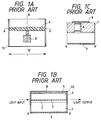
- FIGs. 1A to 1C show a conventional electro- absoprtion optical modulator which is one type of semiconductor optical modulators.
- numeral 1 denotes an n-doped semiconductor wafer
- 2 denotes an n-doped buffer layer
- 3 denotes an undoped light absorption layer
- 4 denotes a p-doped cladding layer
- 5 denotes a contact layer
- 6 denotes an optical waveguide
- 7 denotes an insulator
- 8 denotes a p electrode
- 9 denotes an n electrode
- 10 denotes an anti-reflection coat.
- the optical waveguide has the light absorption layer 3, and light is modulated by applying an electric field to the light absorption layer by use of electrodes and by changing the absorption intensity.
- FIGs. 2A and 2B show an optical modulator package using the above semiconductor optical modulator.
- numeral 21 denotes a package body
- 22 denotes a polarization holding fiber
- 23 denotes a carrier
- 24 denotes an unspherical lens
- 251 and 252 denotes microstrip lines
- 26 denotes an optical modulator
- 27 denotes a matching resistor
- 281 and 282 represent wire bonds
- 29 denotes input/output terminal pins
- 30 denotes a rod lens
- 31 denotes an electronic cooling device
- 32 denotes a package cover.
- optical coupling of the input/output optical fiber 22 and the optical modulator 26 is achieved by the rod lens 30 and unspherical lens 24.
- the element is mounted on the carrier 32 having a protrusion with a width (W) approximately equal to the modulator length (L) so that light is not scattered between the modulator 26 and the unspherical lens 24.
- An electrical signal is fed to the modulator through the microstrip line 251 and moreover, the matching resistor 27 for avoiding reflection of the signal is provided at the end of the strip line 251.
- This type of package is described in, for example, the TECHNICAL REPORT OF IEICE, EMD 93-33, CPM 93-46, OQE 93-67 (1993-08), pp. 55-60.
- the modulation speed of the above optical modulator is limited by the element capacitance. Therefore, to obtain a higher-speed optical modulator, it is necessary to decrease the element capacitance by decreasing the modulator length (L).
- the element has a length of 300 ⁇ m or less
- the light not coupled with the optical waveguide at the incidence facet of the modulator is propagated through the part above the optical modulator or within the wafer of the optical modulator and coupled with an optical fiber on the output side.
- the uncoupled light impairs the extinction characteristics of the package or makes the adjustment of the optical system difficult.
- the above object is achieved by forming a passive region one side or both sides of a modulation region for modulating light in a waveguide-type semiconductor modulator and forming at least part of a cladding layer in the passive region from undoped or semi- insulating semiconductor or electrically isolating the cladding layer in the passive region from the cladding layer in the passive region.
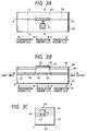
- numeral 41 denotes an n-InP wafer
- 42 denotes an n-InAlAs buffer layer
- 43 denotes an undoped InGaAs/InAlAs strained multiple- quantum well layer
- 44 denotes a p-InAlAs cladding layer
- 45 denotes a p+-InGaAs contact layer
- 46 denotes an SiO2 mask
- 47 denotes an undoped InP buffer layer
- 48 denotes an undoped InGaAsP core layer
- 49 denotes an undoped InP cladding layer
- 50 denotes an optical waveguide
- 51 denotes polyimide
- 52 denotes a Cr/Au p-electrode
- 53 denotes an AuGeNi n-electrode
- 54 denotes an SiNx anti-reflection
- the optical waveguide structure comprises a modulation region (length of L2) for modulating light and two passive regions (lengths of L1 and L3) for coupling the modulation region with the element facets.
- the band gap energy of the semiconductor constituting the optical waveguide in the passive region is sufficiently larger than the light energy, and the light is propagated in these regions with a low loss.
- the light entering through a facet is propagated through the passive region, modulated in the modulation region, propagated through the passive region again, and emitted outside. Because the cladding layer 49 in the passive region is formed of undoped or semi-insulating semiconductor, the element capacitance is not increased even when the passive regions are provided.
- the device has been described above in which optical waveguides are provided on both sides of a modulation region. However, it should be noted that the same effect can be expected by forming an optical waveguide on only one side of the modulation region. Moreover, though the method for insulating the whole of the cladding layer 49 in the passive region has been described above, completely the same effect can be expected by forming high-resistance regions between the passive regions and the modulation region to electrically isolate the cladding layers in both regions from each other even if the cladding layers in the passive regions are conductive.
- FIG. 3A is a top view of the optical modulator of embodiment 1
- FIG. 3B is a sectional view along the line A-A' of FIG. 3A
- FIG. 3C is a sectional view along the line C-C' of FIG. 3A.
- the B-B' cross section in FIG. 3A is the same as that in FIG. 1C.
- Numeral 46 in FIG. 3A denotes an SiO2 mask used for etching and the second crystal growth.
- n-In 0.53 Al 0.47 As buffer layer 42 (0.2 ⁇ m), undoped In 0.48 Ga 0.52 As/In 0.60 Al 0.40 As strained multiple- quantum well layer 43 (well layer: 7 nm, barrier layer: 5 nm, number of wells: 10, and band gap wavelength: 1.49 ⁇ m), p-In 0.53 Al 0.47 As cladding layer 44 (2.0 ⁇ m), and p+-In 0.53 Ga 0.47 As contact layer 45 (0.2 ⁇ m) were formed in order on the n-InP wafer 41 by an MBE (Molecular Beam Epitaxy) technique. Then, the MBE growth layer in the region other than the SiO2 mask 46 was removed by selective wet etching using the SiO2 mask 46.
- MBE Molecular Beam Epitaxy
- the undoped InP buffer layer 47 (0.15 ⁇ m), undoped In 0.82 Ga 0.18 As 0.40 P 0.60 core layer 48 (0.2 ⁇ m), and undoped InP cladding layer 49 (1.5 ⁇ m) were grown in the region other than the SiO2 mask 46 by MOCVD (Metal Organic Chemical Vapor Deposition).
- MOCVD Metal Organic Chemical Vapor Deposition
- mesa-etching up to an InP wafer was performed by dry-etching to form an optical waveguide 50 (waveguide width of 3 ⁇ m).
- the element surface was planarized by polyimide 51, the Cr/Au p-electrode 52 was formed.
- the element After the AuGeNi n-electrode 53 is formed by vacuum-evaporation, the element is cleaved, and SiNx anti-reflection coats 54 are formed on both facets.
- the element had a length of 1,000 ⁇ m, the modulation region had a length (L1) of 100 ⁇ m, and the element had a capacitance of 0.3 pF.
- the optical modulator package shown in FIGs. 2A and 2B similar to a conventional one was fabricated using the thus obtained modulator.
- the carrier protrusion width (W) was 1,000 ⁇ m.
- a semiconductor laser beam of 1.55 ⁇ m was applied to the obtained optical modulator package to measure the modulation characteristics. In this measurement, the incidence polarization was adjusted so that the light in the modulator was propagated in the TE mode.
- the insertion loss in the state that no voltage was applied to the modulator (light output is ON) was 9 dB and the voltage necessary for 15-dB extinction was 1.5 V.
- the modulation band width (f 3dB ) of the optical modulator package was 20 GHz.
- FIG. 6 An optical fiber transmission equipment (transmission rate of 10 Gbits/s) shown in FIG. 6 was manufactured using the obtained optical modulator package.
- numeral 90 denotes a 1.55- ⁇ m DFB laser
- 91 denotes an optical modulator driving circuit
- 92 denotes an optical modulator package
- 93 denotes an optical fiber amplifier
- 94 denotes a dispersion-shift optical fiber.
- the light emitted from the DFB (distributed feedback) laser 90 with a oscillation wavelength of 1.55 ⁇ m was modulated by the optical modulator package 92, amplified by the optical fiber amplifier 93, transmitted through the dispersion-shift optical fiber 94 (100 km), and received by a receiver.
- the error rate of the optical fiber transmission equipment was measured, and a good value of 10-12 or less was obtained.
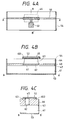
- FIG. 4A is a top view of the optical modulator of embodiment 2, and FIG. 4B is a sectional view along the line A-A' of FIG. 4A.
- the broken line 46 in FIG. 4A shows an SiO2 mask used for the etching and the second crystal growth.
- numeral 61 denotes an n-InP buffer layer
- 62 denotes an undoped In GaAsP absorption layer
- 63 denotes a p-InP cladding layer
- 64 denotes an Fe-doped semi-insulating InP upper cladding layer
- 651 and 652 denote n-InP cap layers
- 66 denotes an Fe-doped semi-insulating InP buried layer.
- n-InP buffer layer 61 (0.2 ⁇ m), undoped In 0.63 Ga 0.37 As 0.82 P 0.18 absorption layer 62 (0.2 ⁇ m, band gap wavelength: 1.47 ⁇ m), p-InP cladding layer 63 (2.0 ⁇ m), and p+-In 0.53 Ga 0.47 As contact layer 45 (0.2 ⁇ m) were formed in order on the n-InP wafer 41 by MOCVD. Then, the contact layer 45, cladding layer 63, and absorption layer 62 other than the SiO2 mask 46 were removed by selective wet etching using the SiO2 mask 46.
- the undoped In 0.82 Ga 0.18 As 0.40 P 0.60 core layer 48 (0.2 ⁇ m), Fe-doped semi-insulating InP cladding layer 64 (2.0 ⁇ m), and n-InP cap layer 651 were formed in the region other than the SiO2 mask 46 by MOCVD (Metal Organic Chemical Vapor Deposition).
- MOCVD Metal Organic Chemical Vapor Deposition
- etching is performed up to the InP wafer 41 by wet etching to form the optical waveguide 50 (waveguide width of 2 ⁇ m) and the waveguide was embedded with the Fe-doped InP 652 and n-InP 652.
- the Cr/Au p-electrode 52 was formed to partly remove the n-InP cap layers in the region other than the electrode. After the AuGeNi n-electrode 53 was vacuum-evaporated, the element was cleaved and the SiNx anti-reflection coats 54 were formed on both facets of the element.
- the element had an overall length of 1,000 ⁇ m, the modulation region has a length of 150 ⁇ m, and the element had a capacitance of 0.4 pF.
- An optical modulator package was manufactured by using the above optical modulator similarly to embodiment 1.
- the carrier protrusion width (W) was 1,000 ⁇ m similarly to embodiment 1.
- the insertion loss of the obtained modulator was 6 dB, the modulation band was 15 GHz, and the voltage necessary for 15-dB extinction was 3.0 V.
- An optical fiber transmission equipment like embodiment 1 was fabricated by using the optical modulator, and it was a good transmission equipment with an error rate of 10 ⁇ 12 or less.
- FIG. 5A is a top view of the optical modulator of embodiment 3, and FIG. 5B is a sectional view along the line A-A' of FIG. 5A.
- the broken lines in FIG. 5A show SiO2 masks 801 and 802 used for crystal growth.
- numeral 81 denotes an n-InGaAsP lower guiding layer
- 82 denotes an InGaAs/InGaAsP multiple- quantum well layer
- 83 denotes a p-InGaAsP upper guiding layer
- 84 denotes a p-InP cladding layer
- 85 denotes proton implantation.
- the SiO2 masks 801 and 802 were provided on an n-InP wafer, and the n-In 0.82 Ga 0.18 As 0.40 P 0.60 lower guiding layer 81 (0.15 ⁇ m), undoped In 0.53 Ga 0.47 As/ In 0.82 Ga 0.18 As 0.40 P 0.60 multiple-quantum well layer 82 (well layer: 4 nm, barrier layer: 7 nm, number of wells: 10, band gap wavelength: 1.45 ⁇ m), and p-In 0.82 Ga 0.18 As 0.40 P 0.60 upper guiding layer 83 (0.15 ⁇ m) were selectively grown in the region other than the SiO2 masks by MOCVD.
- the growth rate and mixed crystal composition were changed due to the material flowing from the tops of the masks, and the band gap wavelength of a multiple quantum well became larger than those of the passive regions.
- the opening widths of the SiO2 masks were adjusted so that the multiple quantum well band gap wavelength in the modulation region was 1.50 ⁇ m.
- a resist mask was placed on the light modulation region to partly remove the contact layer other than the light modulation region. Then, a protons were implanted into the part between the modulation region and the passive region to insulate the passive-region cladding layer from the modulation-region cladding layer.
- Mesa-etching was performed up to the InP wafer 41 by dry etching to form the optical waveguide 50 (waveguide width of 3 ⁇ m), and thereafter planarized with polyimide 51 to form the Cr/Au p-electrode 52.
- the element was cleaved to form the SiNx anti-reflection coats 54 on both facets of the element.
- the element had an overall length of 800 ⁇ m and the modulation region had a length of 100 ⁇ m.
- the obtained element had a capacitance of 0.3 pF.
- An optical module package was manufactured using the above optical modulator in the same manner as of embodiment 1.
- the carrier width (W) was 800 ⁇ m.
- the insertion loss of the obtained optical modulator was 6 dB, the modulation band was 18 GHz, and the voltage necessary for 15-dB extinction was 2.0 V.
- An optical fiber transmission equipment similar to embodiment 1 was made using the optical modulator, and it was a good optical fiber transmission equipment with an error rate of 10 ⁇ 12 or less was obtained.
- optical modulator of the present invention it is possible to enhance the operating speed of an optical modulator package without deteriorating the thermal, high-frequency, and extinction characteristics. Therefore, the operation of an optical fiber transmission equipment can be speeded up by applying the optical modulator of the present invention and the optical modulator package to optical fiber transmission equipment.
Abstract

Description
- The present invention relates to a semiconductor optical modulator, an optical modulator package using the semiconductor optical modulator, and an optical fiber transmission equipment.
- To increase the capacity of an optical fiber transmission equipment, it is necessary to realize higher-speed light modulation. An optical modulator using the electric field effect of semiconductor can operate at a high-speed, high-efficiency light modulation. Therefore, it has been studied how to increase the operating speed of the modulator and to package the modulator in order to apply the modulator to optical fiber transmission equipment.
- FIGs. 1A to 1C show a conventional electro- absoprtion optical modulator which is one type of semiconductor optical modulators. In FIGs. 1A to 1C, numeral 1 denotes an n-doped semiconductor wafer, 2 denotes an n-doped buffer layer, 3 denotes an undoped light absorption layer, 4 denotes a p-doped cladding layer, 5 denotes a contact layer, 6 denotes an optical waveguide, 7 denotes an insulator, 8 denotes a p electrode, 9 denotes an n electrode, and 10 denotes an anti-reflection coat. In this modulator, light enters the optical waveguide from an element facet and is propagated through the optical waveguide, and thereafter it is emitted from the opposite facet. The optical waveguide has the
light absorption layer 3, and light is modulated by applying an electric field to the light absorption layer by use of electrodes and by changing the absorption intensity. By adopting a multiple-quantum well structure in thelight absorption layer 3 so as to utilize the electro- absorption effect, an optical modulator with a higher efficiency is obtained. - FIGs. 2A and 2B show an optical modulator package using the above semiconductor optical modulator. In FIGs. 2A and 2B,
numeral 21 denotes a package body, 22 denotes a polarization holding fiber, 23 denotes a carrier, 24 denotes an unspherical lens, 251 and 252 denotes microstrip lines, 26 denotes an optical modulator, 27 denotes a matching resistor, 281 and 282 represent wire bonds, 29 denotes input/output terminal pins, 30 denotes a rod lens, 31 denotes an electronic cooling device, and 32 denotes a package cover. In the modulator package, optical coupling of the input/outputoptical fiber 22 and theoptical modulator 26 is achieved by therod lens 30 andunspherical lens 24. The element is mounted on thecarrier 32 having a protrusion with a width (W) approximately equal to the modulator length (L) so that light is not scattered between themodulator 26 and theunspherical lens 24. An electrical signal is fed to the modulator through themicrostrip line 251 and moreover, thematching resistor 27 for avoiding reflection of the signal is provided at the end of thestrip line 251. This type of package is described in, for example, the TECHNICAL REPORT OF IEICE, EMD 93-33, CPM 93-46, OQE 93-67 (1993-08), pp. 55-60. - The modulation speed of the above optical modulator is limited by the element capacitance. Therefore, to obtain a higher-speed optical modulator, it is necessary to decrease the element capacitance by decreasing the modulator length (L).
- However, when decreasing the device length (L) of a conventional optical modulator and optical modulator package in order to increase the operation speed, it is necessary to also decrease the width (W) of the protrusion of a carrier in order to avoid scattering of light. However, if the width (W) of the carrier protrusion is decreased, a problem arises that the mechanical strength of the protrusion is decreased or heat conduction becomes low. Moreover, it is necessary to decrease the
microstrip line 251 and the matchingresistor 27 in size provided on the same protrusion, otherwise a problem brings up that the high frequency characteristics of the strip line and the withstand voltage of the matching resistor are impaired. Furthermore, when the element has a length of 300 µm or less, the light not coupled with the optical waveguide at the incidence facet of the modulator is propagated through the part above the optical modulator or within the wafer of the optical modulator and coupled with an optical fiber on the output side. The uncoupled light impairs the extinction characteristics of the package or makes the adjustment of the optical system difficult. - It is an object of the present invention to provide a high-speed semiconductor optical modulator suitable for packaging, an optical modulator package using the optical modulator, and an optical fiber transmission equipment.
- The above object is achieved by forming a passive region one side or both sides of a modulation region for modulating light in a waveguide-type semiconductor modulator and forming at least part of a cladding layer in the passive region from undoped or semi- insulating semiconductor or electrically isolating the cladding layer in the passive region from the cladding layer in the passive region.
- Functions of the optical modulator according to the invention will be described below, referring to FIGs. 3A to 3C. In FIGs. 3A to 3C,
numeral 41 denotes an n-InP wafer, 42 denotes an n-InAlAs buffer layer, 43 denotes an undoped InGaAs/InAlAs strained multiple- quantum well layer, 44 denotes a p-InAlAs cladding layer, 45 denotes a p+-InGaAs contact layer, 46 denotes an SiO₂ mask, 47 denotes an undoped InP buffer layer, 48 denotes an undoped InGaAsP core layer, 49 denotes an undoped InP cladding layer, 50 denotes an optical waveguide, 51 denotes polyimide, 52 denotes a Cr/Au p-electrode, 53 denotes an AuGeNi n-electrode, and 54 denotes an SiNx anti-reflection coat. In this modulator, the optical waveguide structure comprises a modulation region (length of L₂) for modulating light and two passive regions (lengths of L₁ and L₃) for coupling the modulation region with the element facets. The band gap energy of the semiconductor constituting the optical waveguide in the passive region is sufficiently larger than the light energy, and the light is propagated in these regions with a low loss. The light entering through a facet is propagated through the passive region, modulated in the modulation region, propagated through the passive region again, and emitted outside. Because thecladding layer 49 in the passive region is formed of undoped or semi-insulating semiconductor, the element capacitance is not increased even when the passive regions are provided. Therefore, in this optical modulator, it is possible to easily provide a high speed device by decreasing the modulation-region length (L₂) even though the overall device length (
- The device has been described above in which optical waveguides are provided on both sides of a modulation region. However, it should be noted that the same effect can be expected by forming an optical waveguide on only one side of the modulation region. Moreover, though the method for insulating the whole of the
cladding layer 49 in the passive region has been described above, completely the same effect can be expected by forming high-resistance regions between the passive regions and the modulation region to electrically isolate the cladding layers in both regions from each other even if the cladding layers in the passive regions are conductive. -
- FIG. 1A is a top view of a conventional semiconductor optical modulator, FIG. 1B is a sectional view along the line A-A' of FIG. 1A, and FIG. 1C is a sectional view along the line B-B' of FIG. 1A;
- FIG. 2A is a top view of a conventional semiconductor optical modulator package (however, the package cover is removed), and FIG. 2B is a sectional view along the line A-A' of FIG. 2A (the light propagation state is also shown);
- FIG. 3A is a top view of embodiment 1 of the optical modulator of the present invention, FIG. 3B is a sectional view along the line A-A' of FIG. 3A, and FIG. 3C is a sectional view along the line C-C' of FIG. 3A;
- FIG. 4A is a top view of
embodiment 2 of the optical modulator of the present invention, FIG. 4B is a sectional view along the line A-A' of FIG. 4A, and FIG. 4C is a sectional view along the line B-B' of FIG. 4A; - FIG. 5A is a top view of
embodiment 3 of the optical modulator of the present invention, and FIG. 5B is a sectional view along the line A-A' of FIG. 5A; and - FIG. 6 is an illustration showing the optical modulator of the present invention and an optical fiber transmission equipment using the optical modulator.
- FIG. 3A is a top view of the optical modulator of embodiment 1, FIG. 3B is a sectional view along the line A-A' of FIG. 3A, and FIG. 3C is a sectional view along the line C-C' of FIG. 3A. The B-B' cross section in FIG. 3A is the same as that in FIG. 1C.
Numeral 46 in FIG. 3A denotes an SiO2 mask used for etching and the second crystal growth. - The n-In0.53Al0.47As buffer layer 42 (0.2 µm), undoped In0.48Ga0.52As/In0.60Al0.40As strained multiple- quantum well layer 43 (well layer: 7 nm, barrier layer: 5 nm, number of wells: 10, and band gap wavelength: 1.49 µm), p-In0.53Al0.47As cladding layer 44 (2.0 µm), and p+-In0.53Ga0.47As contact layer 45 (0.2 µm) were formed in order on the n-
InP wafer 41 by an MBE (Molecular Beam Epitaxy) technique. Then, the MBE growth layer in the region other than theSiO₂ mask 46 was removed by selective wet etching using theSiO₂ mask 46. Then, the undoped InP buffer layer 47 (0.15 µm), undoped In0.82Ga0.18As0.40P0.60 core layer 48 (0.2 µm), and undoped InP cladding layer 49 (1.5 µm) were grown in the region other than theSiO2 mask 46 by MOCVD (Metal Organic Chemical Vapor Deposition). After the SiO₂ mask is removed, mesa-etching up to an InP wafer was performed by dry-etching to form an optical waveguide 50 (waveguide width of 3 µm). After the element surface was planarized bypolyimide 51, the Cr/Au p-electrode 52 was formed. After the AuGeNi n-electrode 53 is formed by vacuum-evaporation, the element is cleaved, and SiNx anti-reflection coats 54 are formed on both facets. The element had a length of 1,000 µm, the modulation region had a length (L₁) of 100 µm, and the element had a capacitance of 0.3 pF. - The optical modulator package shown in FIGs. 2A and 2B similar to a conventional one was fabricated using the thus obtained modulator. In the case of this modulator package, the carrier protrusion width (W) was 1,000 µm. A semiconductor laser beam of 1.55 µm was applied to the obtained optical modulator package to measure the modulation characteristics. In this measurement, the incidence polarization was adjusted so that the light in the modulator was propagated in the TE mode. The insertion loss in the state that no voltage was applied to the modulator (light output is ON) was 9 dB and the voltage necessary for 15-dB extinction was 1.5 V. The modulation band width (f3dB) of the optical modulator package was 20 GHz.
- An optical fiber transmission equipment (transmission rate of 10 Gbits/s) shown in FIG. 6 was manufactured using the obtained optical modulator package. In FIG. 6, numeral 90 denotes a 1.55-µm DFB laser, 91 denotes an optical modulator driving circuit, 92 denotes an optical modulator package, 93 denotes an optical fiber amplifier, and 94 denotes a dispersion-shift optical fiber. The light emitted from the DFB (distributed feedback)
laser 90 with a oscillation wavelength of 1.55 µm was modulated by theoptical modulator package 92, amplified by theoptical fiber amplifier 93, transmitted through the dispersion-shift optical fiber 94 (100 km), and received by a receiver. The error rate of the optical fiber transmission equipment was measured, and a good value of 10-12 or less was obtained. - FIG. 4A is a top view of the optical modulator of
embodiment 2, and FIG. 4B is a sectional view along the line A-A' of FIG. 4A. Thebroken line 46 in FIG. 4A shows an SiO2 mask used for the etching and the second crystal growth. In FIGs. 4A and 4B, numeral 61 denotes an n-InP buffer layer, 62 denotes an undoped In GaAsP absorption layer, 63 denotes a p-InP cladding layer, 64 denotes an Fe-doped semi-insulating InP upper cladding layer, 651 and 652 denote n-InP cap layers, and 66 denotes an Fe-doped semi-insulating InP buried layer. - The n-InP buffer layer 61 (0.2 µm), undoped In0.63Ga0.37As0.82P0.18 absorption layer 62 (0.2 µm, band gap wavelength: 1.47 µm), p-InP cladding layer 63 (2.0 µm), and p+-In0.53Ga0.47As contact layer 45 (0.2 µm) were formed in order on the n-
InP wafer 41 by MOCVD. Then, thecontact layer 45,cladding layer 63, andabsorption layer 62 other than theSiO₂ mask 46 were removed by selective wet etching using theSiO₂ mask 46. Then, the undoped In0.82Ga0.18As0.40P0.60 core layer 48 (0.2 µm), Fe-doped semi-insulating InP cladding layer 64 (2.0 µm), and n-InP cap layer 651 were formed in the region other than theSiO₂ mask 46 by MOCVD (Metal Organic Chemical Vapor Deposition). After theSiO₂ mask 46 was removed, etching is performed up to theInP wafer 41 by wet etching to form the optical waveguide 50 (waveguide width of 2 µm) and the waveguide was embedded with the Fe-dopedInP 652 and n-InP 652. The Cr/Au p-electrode 52 was formed to partly remove the n-InP cap layers in the region other than the electrode. After the AuGeNi n-electrode 53 was vacuum-evaporated, the element was cleaved and the SiNx anti-reflection coats 54 were formed on both facets of the element. The element had an overall length of 1,000 µm, the modulation region has a length of 150 µm, and the element had a capacitance of 0.4 pF. - An optical modulator package was manufactured by using the above optical modulator similarly to embodiment 1. The carrier protrusion width (W) was 1,000 µm similarly to embodiment 1. The insertion loss of the obtained modulator was 6 dB, the modulation band was 15 GHz, and the voltage necessary for 15-dB extinction was 3.0 V.
- An optical fiber transmission equipment like embodiment 1 was fabricated by using the optical modulator, and it was a good transmission equipment with an error rate of 10⁻¹² or less.
- FIG. 5A is a top view of the optical modulator of
embodiment 3, and FIG. 5B is a sectional view along the line A-A' of FIG. 5A. The broken lines in FIG. 5A show SiO₂ masks 801 and 802 used for crystal growth. In FIG. 5B, numeral 81 denotes an n-InGaAsP lower guiding layer, 82 denotes an InGaAs/InGaAsP multiple- quantum well layer, 83 denotes a p-InGaAsP upper guiding layer, 84 denotes a p-InP cladding layer, and 85 denotes proton implantation. - The SiO₂ masks 801 and 802 were provided on an n-InP wafer, and the n-In0.82Ga0.18As0.40P0.60 lower guiding layer 81 (0.15 µm), undoped In0.53Ga0.47As/ In0.82Ga0.18As0.40P0.60 multiple-quantum well layer 82 (well layer: 4 nm, barrier layer: 7 nm, number of wells: 10, band gap wavelength: 1.45 µm), and p-In0.82Ga0.18As0.40P0.60 upper guiding layer 83 (0.15 µm) were selectively grown in the region other than the SiO₂ masks by MOCVD. In this case, in the modulation region sandwiched by the SiO₂ masks 801 and 802, the growth rate and mixed crystal composition were changed due to the material flowing from the tops of the masks, and the band gap wavelength of a multiple quantum well became larger than those of the passive regions. In the above case, however, the opening widths of the SiO₂ masks were adjusted so that the multiple quantum well band gap wavelength in the modulation region was 1.50 µm. After the SiO₂ masks 801 and 802 were removed, the p-InP cladding layer 49 (2.0 µm) and p+-In0.53Ga0.47As contact layer 45 (0.2 µm) were formed on the entire surface of the wafer by MOCVD. A resist mask was placed on the light modulation region to partly remove the contact layer other than the light modulation region. Then, a protons were implanted into the part between the modulation region and the passive region to insulate the passive-region cladding layer from the modulation-region cladding layer. Mesa-etching was performed up to the
InP wafer 41 by dry etching to form the optical waveguide 50 (waveguide width of 3 µm), and thereafter planarized withpolyimide 51 to form the Cr/Au p-electrode 52. After forming the AuGeNi n-electrode 53, the element was cleaved to form the SiNx anti-reflection coats 54 on both facets of the element. The element had an overall length of 800 µm and the modulation region had a length of 100 µm. The obtained element had a capacitance of 0.3 pF. - An optical module package was manufactured using the above optical modulator in the same manner as of embodiment 1. The carrier width (W) was 800 µm. The insertion loss of the obtained optical modulator was 6 dB, the modulation band was 18 GHz, and the voltage necessary for 15-dB extinction was 2.0 V.
- An optical fiber transmission equipment similar to embodiment 1 was made using the optical modulator, and it was a good optical fiber transmission equipment with an error rate of 10⁻¹² or less was obtained.
- Though the invention was applied to only an electro-absorption-type intensity modulators, it will be obvious that the present invention can be generally applied to waveguide-type optical modulators (e.g. phase modulators).
- By using the optical modulator of the present invention, it is possible to enhance the operating speed of an optical modulator package without deteriorating the thermal, high-frequency, and extinction characteristics. Therefore, the operation of an optical fiber transmission equipment can be speeded up by applying the optical modulator of the present invention and the optical modulator package to optical fiber transmission equipment.
Claims (13)
- A semiconductor optical modulator comprising a semiconductor wafer (41), and an optical waveguide (50), which is formed on the semiconductor wafer and comprises a modulation region for modulating light and a passive region for propagating light on one side or both sides of the modulation region.
- The modulator of claim 1, wherein the modulation region of the optical waveguide has a length L₂ of less than 300 µm and the optical waveguide has an overall length (

- The modulator of claim 1 or 2, wherein at least part of the cladding layer (49), in the passive region is made of undoped semiconductor or semi-insulating semiconductor.
- The modulator of any preceding claim, wherein the cladding layer (49) in the passive region is electrically isolated from the cladding layer in the modulation region.
- The modulator of any preceding claim, wherein light is modulated by use of the electro-absorption effect of semiconductor.
- The modulator of any preceding claim, wherein at least part of the optical waveguide comprises a multiple-quantum well (82).
- The modulator of any preceding claim, wherein at least part of the optical waveguide comprises a strained multiple-quantum well (82).
- The modulator of any preceding claim, wherein a multilayer structure serving as an optical waveguide in the modulation region is provided on the entire surface of the wafer, at least part of the multilayer structure in the passive region is removed, and a multilayer structure constituting at least part of an optical waveguide in the passive region is formed in the passive region again.
- The modulator of any preceding claim, wherein at least part of multilayer structures constituting the optical waveguides in the absorption and passive regions are simultaneously formed by selective-area growth with an insulating mask placed on the semiconductor.
- The modulator of any preceding claim, wherein semiconductor doped with Fe or semiconductor into which protons are implanted is used.
- An optical modulator package using the semiconductor optical modulator of any preceding claim.
- The modulator package of claim 11, wherein a protrusion of a carrier on which a modulator is mounted has a width of 300 µm or more.
- An optical fiber transmission equipment using the optical modulator package of claim 11 or 12.
Applications Claiming Priority (3)
| Application Number | Priority Date | Filing Date | Title |
|---|---|---|---|
| JP20876/94 | 1994-02-18 | ||
| JP2087694 | 1994-02-18 | ||
| JP6020876A JPH07230066A (en) | 1994-02-18 | 1994-02-18 | Semiconductor optical modulator |
Publications (2)
| Publication Number | Publication Date |
|---|---|
| EP0672932A1 true EP0672932A1 (en) | 1995-09-20 |
| EP0672932B1 EP0672932B1 (en) | 2001-06-06 |
Family
ID=12039393
Family Applications (1)
| Application Number | Title | Priority Date | Filing Date |
|---|---|---|---|
| EP95101929A Expired - Lifetime EP0672932B1 (en) | 1994-02-18 | 1995-02-13 | Semiconductor optical modulator |
Country Status (4)
| Country | Link |
|---|---|
| US (1) | US5742423A (en) |
| EP (1) | EP0672932B1 (en) |
| JP (1) | JPH07230066A (en) |
| DE (1) | DE69521163T2 (en) |
Cited By (1)
| Publication number | Priority date | Publication date | Assignee | Title |
|---|---|---|---|---|
| US5742423A (en) * | 1994-02-18 | 1998-04-21 | Hitachi, Ltd. | Semiconductor optical modulator |
Families Citing this family (14)
| Publication number | Priority date | Publication date | Assignee | Title |
|---|---|---|---|---|
| JP2955986B2 (en) * | 1996-05-22 | 1999-10-04 | 日本電気株式会社 | Semiconductor optical modulator and method of manufacturing the same |
| JPH1096879A (en) * | 1996-09-20 | 1998-04-14 | Nec Corp | Semiconductor optical modulator and optical communication device formed by using the same |
| CA2218262C (en) * | 1996-10-17 | 2001-04-24 | Kenji Kawano | Ultra-high-speed semiconductor optical modulator with traveling-wave electrode |
| WO1999016193A1 (en) | 1997-09-19 | 1999-04-01 | Hitachi, Ltd. | Optical communication equipment and system |
| JP3723333B2 (en) * | 1997-09-29 | 2005-12-07 | 日本碍子株式会社 | Light modulator |
| US6396801B1 (en) | 1998-03-17 | 2002-05-28 | Trw Inc. | Arbitrary waveform modem |
| US6466349B1 (en) * | 1998-05-14 | 2002-10-15 | Hughes Electronics Corporation | Integrated optical transmitter |
| KR100333482B1 (en) | 1999-09-15 | 2002-04-25 | 오길록 | High speed semiconductor optical modulator and its fabrication method |
| US6421161B1 (en) | 2001-01-18 | 2002-07-16 | The Boeing Company | Fiber modulator and associated method |
| US7120183B2 (en) | 2001-07-11 | 2006-10-10 | Optium Corporation | Electro-absorption modulated laser with high operating temperature tolerance |
| US6804421B2 (en) * | 2002-01-25 | 2004-10-12 | T-Networks, Inc. | Monolithic expanded beam mode electroabsorption modulator |
| JP2011203662A (en) * | 2010-03-26 | 2011-10-13 | Mitsubishi Electric Corp | Optical modulator, and method of manufacturing the same |
| US8410566B2 (en) * | 2011-07-21 | 2013-04-02 | Kotura, Inc. | Application of electrical field power to light-transmitting medium |
| US9153940B2 (en) * | 2013-11-26 | 2015-10-06 | Taiwan Semiconductor Manufacturing Company, Ltd. | Electro-optic modulator device and method of making the same |
Citations (2)
| Publication number | Priority date | Publication date | Assignee | Title |
|---|---|---|---|---|
| JPH0274918A (en) * | 1988-09-12 | 1990-03-14 | Nippon Telegr & Teleph Corp <Ntt> | Optical device with wave guide |
| JPH0529602A (en) * | 1991-07-22 | 1993-02-05 | Hitachi Ltd | Semiconductor optical integrated element and manufacture thereof |
Family Cites Families (7)
| Publication number | Priority date | Publication date | Assignee | Title |
|---|---|---|---|---|
| US4802182A (en) * | 1987-11-05 | 1989-01-31 | Xerox Corporation | Monolithic two dimensional waveguide coupled cavity laser/modulator |
| JPH03293622A (en) * | 1990-04-12 | 1991-12-25 | Hitachi Ltd | Optical modulator |
| US5165105A (en) * | 1991-08-02 | 1992-11-17 | Minnesota Minning And Manufacturing Company | Separate confinement electroabsorption modulator utilizing the Franz-Keldysh effect |
| US5222162A (en) * | 1991-11-27 | 1993-06-22 | Hughes Aircraft Company | Monolithic integrated optical time delay network for antenna beam steering |
| JP2739666B2 (en) * | 1992-06-11 | 1998-04-15 | 国際電信電話株式会社 | Light modulation element |
| US5347601A (en) * | 1993-03-29 | 1994-09-13 | United Technologies Corporation | Integrated optical receiver/transmitter |
| JPH07230066A (en) * | 1994-02-18 | 1995-08-29 | Hitachi Ltd | Semiconductor optical modulator |
-
1994
- 1994-02-18 JP JP6020876A patent/JPH07230066A/en active Pending
-
1995
- 1995-02-13 EP EP95101929A patent/EP0672932B1/en not_active Expired - Lifetime
- 1995-02-13 DE DE69521163T patent/DE69521163T2/en not_active Expired - Fee Related
- 1995-02-17 US US08/390,794 patent/US5742423A/en not_active Expired - Fee Related
Patent Citations (2)
| Publication number | Priority date | Publication date | Assignee | Title |
|---|---|---|---|---|
| JPH0274918A (en) * | 1988-09-12 | 1990-03-14 | Nippon Telegr & Teleph Corp <Ntt> | Optical device with wave guide |
| JPH0529602A (en) * | 1991-07-22 | 1993-02-05 | Hitachi Ltd | Semiconductor optical integrated element and manufacture thereof |
Non-Patent Citations (6)
| Title |
|---|
| AOKI M ET AL: "New photonic device integration by selective-area MOVPE and its application to optical modulator/laser integration", MICROWAVE AND OPTICAL TECHNOLOGY LETTERS, 20 FEB. 1994, USA, vol. 7, no. 3, ISSN 0895-2477, pages 132 - 139 * |
| IDO T ET AL: "High-speed MQW electroabsorption optical modulators integrated with low-loss waveguides", IEEE PHOTONICS TECHNOLOGY LETTERS, FEB. 1995, USA, vol. 7, no. 2, ISSN 1041-1135, pages 170 - 172, XP011427278, DOI: doi:10.1109/68.345912 * |
| PATENT ABSTRACTS OF JAPAN vol. 014, no. 267 (P - 1058) 8 June 1990 (1990-06-08) * |
| PATENT ABSTRACTS OF JAPAN vol. 017, no. 313 (E - 1381) 15 June 1993 (1993-06-15) * |
| SASAKI T ET AL: "Novel structure photonic devices using selective MOVPE growth", NEC RESEARCH AND DEVELOPMENT, JULY 1992, JAPAN, vol. 33, no. 3, ISSN 0547-051X, pages 372 - 382, XP000327432 * |
| SHIMIZU H ET AL: "Electroabsorption modulator module", TECHNICAL REPORT OF IEICE, EMD93-33, CPM93-46, OQE93-67, vol. 93, no. 199, JAPAN, pages 55 - 60 * |
Cited By (1)
| Publication number | Priority date | Publication date | Assignee | Title |
|---|---|---|---|---|
| US5742423A (en) * | 1994-02-18 | 1998-04-21 | Hitachi, Ltd. | Semiconductor optical modulator |
Also Published As
| Publication number | Publication date |
|---|---|
| JPH07230066A (en) | 1995-08-29 |
| EP0672932B1 (en) | 2001-06-06 |
| DE69521163D1 (en) | 2001-07-12 |
| DE69521163T2 (en) | 2002-02-28 |
| US5742423A (en) | 1998-04-21 |
Similar Documents
| Publication | Publication Date | Title |
|---|---|---|
| Zhang et al. | 25 GHz polarization-insensitive electroabsorption modulators with traveling-wave electrodes | |
| US5147825A (en) | Photonic-integrated-circuit fabrication process | |
| US5825047A (en) | Optical semiconductor device | |
| US6872966B2 (en) | Optical semiconductor device | |
| US5742423A (en) | Semiconductor optical modulator | |
| US6639241B2 (en) | Optical device using semiconductor | |
| JPH0715000A (en) | Constitution of integrated monolithic laser modulator of multiple quantum well structure | |
| US5889913A (en) | Optical semiconductor device and method of fabricating the same | |
| JP3885528B2 (en) | Light modulator | |
| EP0917260B1 (en) | Electrical isolation of opto-electronic device components | |
| EP0405800A2 (en) | Laser-photodetector assemblage | |
| US5179567A (en) | Semiconductor laser device, method of fabricating the same and optical system of utilizing the same | |
| CA2165711C (en) | Semiconductor light source having a spectrally broad, high power optical output | |
| JPH01319986A (en) | Semiconductor laser device | |
| WO2001013479A1 (en) | Modulator and integrated circuit | |
| JPH06112595A (en) | Fabrication of semiconductor optical functional element | |
| JP2605911B2 (en) | Optical modulator and photodetector | |
| EP1372229B1 (en) | Integrated semiconductor laser and waveguide device | |
| JP2508332B2 (en) | Integrated optical modulator | |
| JP2760276B2 (en) | Selectively grown waveguide type optical control device | |
| JP2000258739A (en) | Optical modulator and light source for optical communication | |
| CN112350148B (en) | Semiconductor optical element and semiconductor optical device including the same | |
| EP1227361A2 (en) | Semiconductor optical device having reduced parasitic capacitance | |
| Kotaka et al. | High‐speed (20 Gb/s), low‐drive voltage (2 Vp‐p) strained InGaAsP mqw modulator/DFB laser light source | |
| JPH1124020A (en) | Embedded type semiconductor optical function element |
Legal Events
| Date | Code | Title | Description |
|---|---|---|---|
| PUAI | Public reference made under article 153(3) epc to a published international application that has entered the european phase |
Free format text: ORIGINAL CODE: 0009012 |
|
| AK | Designated contracting states |
Kind code of ref document: A1 Designated state(s): DE FR GB |
|
| 17P | Request for examination filed |
Effective date: 19960312 |
|
| 17Q | First examination report despatched |
Effective date: 19990128 |
|
| GRAG | Despatch of communication of intention to grant |
Free format text: ORIGINAL CODE: EPIDOS AGRA |
|
| GRAG | Despatch of communication of intention to grant |
Free format text: ORIGINAL CODE: EPIDOS AGRA |
|
| GRAH | Despatch of communication of intention to grant a patent |
Free format text: ORIGINAL CODE: EPIDOS IGRA |
|
| GRAH | Despatch of communication of intention to grant a patent |
Free format text: ORIGINAL CODE: EPIDOS IGRA |
|
| GRAA | (expected) grant |
Free format text: ORIGINAL CODE: 0009210 |
|
| AK | Designated contracting states |
Kind code of ref document: B1 Designated state(s): DE FR GB |
|
| REF | Corresponds to: |
Ref document number: 69521163 Country of ref document: DE Date of ref document: 20010712 |
|
| ET | Fr: translation filed | ||
| REG | Reference to a national code |
Ref country code: GB Ref legal event code: IF02 |
|
| PGFP | Annual fee paid to national office [announced via postgrant information from national office to epo] |
Ref country code: FR Payment date: 20020118 Year of fee payment: 8 |
|
| PGFP | Annual fee paid to national office [announced via postgrant information from national office to epo] |
Ref country code: GB Payment date: 20020201 Year of fee payment: 8 |
|
| PLBE | No opposition filed within time limit |
Free format text: ORIGINAL CODE: 0009261 |
|
| STAA | Information on the status of an ep patent application or granted ep patent |
Free format text: STATUS: NO OPPOSITION FILED WITHIN TIME LIMIT |
|
| PGFP | Annual fee paid to national office [announced via postgrant information from national office to epo] |
Ref country code: DE Payment date: 20020423 Year of fee payment: 8 |
|
| 26N | No opposition filed | ||
| PG25 | Lapsed in a contracting state [announced via postgrant information from national office to epo] |
Ref country code: GB Free format text: LAPSE BECAUSE OF NON-PAYMENT OF DUE FEES Effective date: 20030213 |
|
| PG25 | Lapsed in a contracting state [announced via postgrant information from national office to epo] |
Ref country code: DE Free format text: LAPSE BECAUSE OF NON-PAYMENT OF DUE FEES Effective date: 20030902 |
|
| GBPC | Gb: european patent ceased through non-payment of renewal fee | ||
| PG25 | Lapsed in a contracting state [announced via postgrant information from national office to epo] |
Ref country code: FR Free format text: LAPSE BECAUSE OF NON-PAYMENT OF DUE FEES Effective date: 20031031 |
|
| REG | Reference to a national code |
Ref country code: FR Ref legal event code: ST |