EP0676749A2 - Information reproducing device and method - Google Patents
Information reproducing device and method Download PDFInfo
- Publication number
- EP0676749A2 EP0676749A2 EP95201397A EP95201397A EP0676749A2 EP 0676749 A2 EP0676749 A2 EP 0676749A2 EP 95201397 A EP95201397 A EP 95201397A EP 95201397 A EP95201397 A EP 95201397A EP 0676749 A2 EP0676749 A2 EP 0676749A2
- Authority
- EP
- European Patent Office
- Prior art keywords
- recording medium
- recording
- light
- information
- optical probe
- Prior art date
- Legal status (The legal status is an assumption and is not a legal conclusion. Google has not performed a legal analysis and makes no representation as to the accuracy of the status listed.)
- Granted
Links
Images
Classifications
-
- G—PHYSICS
- G11—INFORMATION STORAGE
- G11B—INFORMATION STORAGE BASED ON RELATIVE MOVEMENT BETWEEN RECORD CARRIER AND TRANSDUCER
- G11B7/00—Recording or reproducing by optical means, e.g. recording using a thermal beam of optical radiation by modifying optical properties or the physical structure, reproducing using an optical beam at lower power by sensing optical properties; Record carriers therefor
- G11B7/004—Recording, reproducing or erasing methods; Read, write or erase circuits therefor
- G11B7/005—Reproducing
-
- G—PHYSICS
- G11—INFORMATION STORAGE
- G11B—INFORMATION STORAGE BASED ON RELATIVE MOVEMENT BETWEEN RECORD CARRIER AND TRANSDUCER
- G11B11/00—Recording on or reproducing from the same record carrier wherein for these two operations the methods are covered by different main groups of groups G11B3/00 - G11B7/00 or by different subgroups of group G11B9/00; Record carriers therefor
-
- G—PHYSICS
- G11—INFORMATION STORAGE
- G11B—INFORMATION STORAGE BASED ON RELATIVE MOVEMENT BETWEEN RECORD CARRIER AND TRANSDUCER
- G11B7/00—Recording or reproducing by optical means, e.g. recording using a thermal beam of optical radiation by modifying optical properties or the physical structure, reproducing using an optical beam at lower power by sensing optical properties; Record carriers therefor
- G11B7/004—Recording, reproducing or erasing methods; Read, write or erase circuits therefor
- G11B7/0045—Recording
- G11B7/00455—Recording involving reflectivity, absorption or colour changes
-
- G—PHYSICS
- G11—INFORMATION STORAGE
- G11B—INFORMATION STORAGE BASED ON RELATIVE MOVEMENT BETWEEN RECORD CARRIER AND TRANSDUCER
- G11B7/00—Recording or reproducing by optical means, e.g. recording using a thermal beam of optical radiation by modifying optical properties or the physical structure, reproducing using an optical beam at lower power by sensing optical properties; Record carriers therefor
- G11B7/004—Recording, reproducing or erasing methods; Read, write or erase circuits therefor
- G11B7/005—Reproducing
- G11B7/0052—Reproducing involving reflectivity, absorption or colour changes
-
- G—PHYSICS
- G11—INFORMATION STORAGE
- G11B—INFORMATION STORAGE BASED ON RELATIVE MOVEMENT BETWEEN RECORD CARRIER AND TRANSDUCER
- G11B7/00—Recording or reproducing by optical means, e.g. recording using a thermal beam of optical radiation by modifying optical properties or the physical structure, reproducing using an optical beam at lower power by sensing optical properties; Record carriers therefor
- G11B7/12—Heads, e.g. forming of the optical beam spot or modulation of the optical beam
- G11B7/135—Means for guiding the beam from the source to the record carrier or from the record carrier to the detector
- G11B7/1384—Fibre optics
-
- G—PHYSICS
- G11—INFORMATION STORAGE
- G11B—INFORMATION STORAGE BASED ON RELATIVE MOVEMENT BETWEEN RECORD CARRIER AND TRANSDUCER
- G11B9/00—Recording or reproducing using a method not covered by one of the main groups G11B3/00 - G11B7/00; Record carriers therefor
- G11B9/12—Recording or reproducing using a method not covered by one of the main groups G11B3/00 - G11B7/00; Record carriers therefor using near-field interactions; Record carriers therefor
- G11B9/14—Recording or reproducing using a method not covered by one of the main groups G11B3/00 - G11B7/00; Record carriers therefor using near-field interactions; Record carriers therefor using microscopic probe means, i.e. recording or reproducing by means directly associated with the tip of a microscopic electrical probe as used in Scanning Tunneling Microscopy [STM] or Atomic Force Microscopy [AFM] for inducing physical or electrical perturbations in a recording medium; Record carriers or media specially adapted for such transducing of information
-
- B—PERFORMING OPERATIONS; TRANSPORTING
- B82—NANOTECHNOLOGY
- B82Y—SPECIFIC USES OR APPLICATIONS OF NANOSTRUCTURES; MEASUREMENT OR ANALYSIS OF NANOSTRUCTURES; MANUFACTURE OR TREATMENT OF NANOSTRUCTURES
- B82Y10/00—Nanotechnology for information processing, storage or transmission, e.g. quantum computing or single electron logic
-
- B—PERFORMING OPERATIONS; TRANSPORTING
- B82—NANOTECHNOLOGY
- B82Y—SPECIFIC USES OR APPLICATIONS OF NANOSTRUCTURES; MEASUREMENT OR ANALYSIS OF NANOSTRUCTURES; MANUFACTURE OR TREATMENT OF NANOSTRUCTURES
- B82Y20/00—Nanooptics, e.g. quantum optics or photonic crystals
-
- G—PHYSICS
- G01—MEASURING; TESTING
- G01Q—SCANNING-PROBE TECHNIQUES OR APPARATUS; APPLICATIONS OF SCANNING-PROBE TECHNIQUES, e.g. SCANNING PROBE MICROSCOPY [SPM]
- G01Q80/00—Applications, other than SPM, of scanning-probe techniques
Definitions
- This invention relates to a novel information processing device and an information processing method which perform recording or erazing of information by voltage application and perform reproduction of information by detecting an evanescent wave.
- the present invention relates to an information processing device and an information processing method which is improved in S/N ratio in reproduction of information which is performed by detecting an evanescent wave.
- NFOM near field scanning optical microscope
- the limit of recording capacity is 108 bit/cm2, which is becoming no longer sufficient for image recording in computers or video instruments in recent years, etc.
- the bit size of recording may be on atomic/molecular order(0.5 to 50 nm)
- the influence of the recorded state on the tunnel current is local, whereby reproduction can be done with difficulty.
- it since there is also the possibility to change the recorded state by the operation of reproduction, it can hardly be said as sufficiently applicable to application for memory.
- an object of the present invention is to provide an information processing device and an information processing method enabling stable writing and reading of information, which are processings of information utilizing evanescnt wave.
- the present invention is an information processing device, comprising a recording medium having a recording layer provided on a substrate which transmits an electromagnetic wave and has electroconductivity, an electroconductive optical probe arranged proximate to said recording layer of said recording medium, a means for applying voltage between said substrate and said optical probe, a means for irradiating an electromagnetic wave on said substrate and a means for detecting the electromagnetic wave entering said optical probe.
- the present invention is an information processing device comprising a recording medium having a recording layer provided on a substrate which transmits an electromagnetic wave and has electroconductivity, an electroconductive optical probe arranged proximate to said recording layer of said recording medium, a means for applying voltage between said substrate and said optical probe, a means for irradiating electromagnetic waves with a plurality of wavelengths on said substrte and a means for detecting the electromagnetic waves with the plurality of wavelengths entering said optical probe.
- the present invention is an information processing method which comprises recording an information by approximating an electroconductive optical probe to a recording medium having a recording layer provided on a substrate which transmits an electromagnetic wave and has electroconductivity and applying a voltage between said substrate and said optical probe, and reading the recorded information by irradiating an electromagnetic wave on said recording medium from said substrate side and detecting the electromagnetic wave oozed out on the surface of said recording medium by said optical probe.
- the present invention is an information processing method, which comprises recording an information by approximating an electroconductive optical probe to a recording medium having a recording layer provided on a substrate which transmits an electromagnetic wave and has electroconductivity and applying a voltage between said substrate and said optical probe, and reading the recorded information by irradiating electromagnetic waves with a plurality of wavelengths on said recording medium from said substrate side and detecting the electromagnetic waves oozed out on the surface of said recording medium by said optical probe.
- the present invention is an information processing device, comprising a recording medium having an information recorded thereon, an optical probe arranged proximate to one side of said recording medium, a means for irradiating electromagnetic waves with a plurality of wavelengths to the other side of said recording medium and a means for detecting the electromagnetic waves with the plurality of wavelengths entering said optical probe.
- the present invention is an information processing method, which comprises irradiating electromagnetic waves with a plurality of wavelengths on the back surface of a recording medium having an information recorded thereon, and reading the recorded information by detecting the electromagnetic waves with the plurality of wavelengths oozed out on the surface of said recording medium.
- STM utilizes the phenomenon that a tunnel current will flow when a probe of a metal (probe electrode) and an electroconductive substance are approached to a distance of about 1 nm with an application of a voltage therebetween. Such current is very sensitive to the distance change therebetween, and by scanning the probe so as to maintain constantly the tunnel current, the surface structure of the real space can be drawn and at the same time various informations concerning all the electron cloud of the surface atom can be read. In this case, the resolving power in the interplanar direction is about 0.1 nm. Therefore, by utilizing the principle of STM, it is possible to perform high density recording sufficiently at the atomic order (sub-nanometer). For example, when the bit size of recording is made 10 nm, a recording device with a density as high as 1012bit/cm2 is obtained.
- PSTM which is further development of STM utilizes the weak light leaked out from the surface of the sample.
- a laser is permitted to enter from the backside of the sample through a prism, and the angle is controlled so that the laser may be totally reflected at the back surface of the sample. Most of the light is reflected, but only a part will pass through the surface to the surface side by the tunnel effect in spite of the condition of total reflection. This is the light called "evanescent wave", with the wavelength being equal to the incident light and the intensity becoming about 1/1000 to 1/100,000 of that of the incident light.
- the intensity of evanescent wave is weaker as farther from the surface of the sample, and by approximating the optical fiber to the sample surface and scanning it while moving so as to detect the evanescent wave with the same intensity, the structure of the surface on the basis of such movement and at the same time through light absorption, spectral information of the sample itself can be examined.
- the resolving power in the interplanar direction is about 1 nm. Therefore, by applying PSTM, it is possible to perform reproduction of a high density recording medium sufficiently on the order of nanometer. Also, in reproduction by use of light, even a recorded state in which a part of the structure within the molecule may locally change can be observed as the change of the light absorption wavelength of the whole molecule.
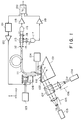
- Fig. 1 is a block diagram showing the constitution of the information processing device according to an example of the present invention.
- Fig. 1 as the recording medium 102, for example, built-up films of monomolecular film layer are formed according to the Langmuir-Blodgett method by use of 10,12-pentacosadiynic acid CH3(CH2)11C ⁇ C-C ⁇ C(CHC2)8COOH, amphiphilic diacetylene derivative, on the surface of an electroconductive prism 101 and a polymer is formed by irradiation of X-ray or gamma-ray.
- the material for the electroconductive prism 101 Ag2O-AgI-MoO3(P2O5) type super-ion conducting glass, a glass containing a polyvalent element such as palladium, iron, etc., or one coated on the glass surface with a thin film composed mainly of SnO2 may be employed.
- the light with wavelength ⁇ 1 generated from the light source 103 and the light with wavelength ⁇ 2 generated from the light source 104 are respectively passed through the beam expanders 105, 106 and the beam mixer 107 to be combined, and permitted to enter the surface of the recording medium 102 in contact with the electroconductive prism 101 under the total reflection condition.
- the electroconductive optical probe 109 is approximated to a distance of about sub-nanometer to the desired position of the recording medium 102.
- the electroconductive optical probe one prepared by polishing one end of the optical fiber made of the same material as the electroconductive prism 101 to have the tip end pointed (radius of curvature ⁇ 1 ⁇ m) is used.
- the evanescent light 100 having thus passed through the recording medium 102 to be oozed out (existing only in the vicinity of the surface) is detected by the electroconductive optical probe 109, introduced into the optical fiber 111, passed through the lens 112, the beam splitter 113, the filters 114, 115 to be divided into the components with wavelengths ⁇ 1 and ⁇ 2, which are respectively converted by photo-multipliers 116, 117 into electrical signals.
- the electrical signals are amplified in the amplifiers 118, 119 (I1, I2), then inputted in the dividing circuit 120 to make the ratio I2/I1 of the two signals the reproduction signal.
- the Z-directional position control of the optical probe 109 during recording and reproduction is performed as follows.
- the signal I1 for the detection light intensity of the wavelength ⁇ 1 is inputted in the feed-back circuit 121, the deviation from the set (light intensity) value is calculated, and after amplification in the amplification circuit 122, as the Z position control signal, by the xyz position control device 108, the Z-directional position of the optical probe 109 is controlled so as to become the set light intensity.
- the optical probe 109 is moved to the desired position of the recording medium 102, and a pulse voltage for recording is applied by the recording signal circuit 124 between the electroconductive optical probe 109 and the electroconductive prism 101 to inject locally electrons into the recording medium. Then, a structural change takes place in the diacetylene derivative polymer through the Joule's heat by the local current, whereby the peak of the absorption band of light is shifted from 640 nm to 580 nm.
- a material of which the absorption band of light can be shifted by electron injection or Joule's heat by current may be available, and otherwise, one decomposable by current Joule's heat such as J associated product of a dye such as squarilium bis-6 octylazulene, etc. (absorption band at wavelength 579 nm to be shifted to 890 nm), or one reduced as follows by electron injection such as polyimide: or one which is greatly changed in absorbance at around 800 nm by intramolecular charge transfer such as copper tetracyanoquinodimethane by electron injection as shown below: may be employed.
Abstract
Description
- This application is a divisional application of our copending European patent application No. 91307007.4.
- This invention relates to a novel information processing device and an information processing method which perform recording or erazing of information by voltage application and perform reproduction of information by detecting an evanescent wave.
- Also, the present invention relates to an information processing device and an information processing method which is improved in S/N ratio in reproduction of information which is performed by detecting an evanescent wave.
- In recent years, uses of memory materials constitute nuclei of elecronics industries such as computers and their related instruments, video discs, digital audiodiscs, etc., and the developments of such materials have been extremely actively progressed. The performances demanded for memory materials, which depend on the uses, may include generally:
- (1) high density and large recording capacity;
- (2) rapid response speed of recording and reproduction;
- (3) small power consumption;
- (4) high productivity and low cost, etc.
- These materials have been heretofore primarily semiconductor memories or magnetic memories by use of magnetic materials or semiconductors as the base material, but with the progress of the laser technique in recent years, inexpensive and high density recording medium with an optical memory by use of an organic thin film such as organic dye, photopolymer, etc. has been developed.
- On the other hand, the scanning tunneling microscopy (hereinafter abbreviated as STM) that can observe directly the electron structure of surface atoms/molecules of a conductor with a resolving power of 0.1 nm has been developed [G. Binnig et al., Phys. Rev. Lett. 49, 57 (1982)]. There has been made the proposal concerning the recording-reproduction device which performs writing-reading onto a recording medium with a bit size of atomic/molecular order (0.5 to 50 nm) by use of the tunnel current applying the principle of STM [for example, Japanese Patent Application Laid-Open Nos. 63-161552 and 63-161553].
- Also, as further development of STM, there have been developed a near field scanning optical microscope (NFOM) which examines the surface state of a sample by utilizing the evanescent wave oozed out from a fine opening smaller than the wavelength of the light at the pointed tip end of a probe to which light introduced from the opposite direction [Duerig et al., is J. Appl. Phys., 59, 3318 (1986)] or the photon scanning tunneling microscopy(PSTM) that permits light to enter from the back surface of a sample through a prism under the condition of total reflection, and detecting the evanescent wave oozed out to the sample surface [Reddick et al., Phys. Rev. B39, 767 (1989)]. By applying the principle of NFOM and utilizing evanescent wave, there has been made a proposal concerning a recording-reproduction device which performs writing onto recording medium and reading therefrom [U.S. Patent 4684206].
- However, of those which have been practically applied in the above prior art examples, even in the optical memory with the highest density and the largest recording capacity, the limit of recording capacity is 10⁸ bit/cm², which is becoming no longer sufficient for image recording in computers or video instruments in recent years, etc.
- In an attempt which performs recording and reproduction by accessing to one molecule, although the bit size of recording may be on atomic/molecular order(0.5 to 50 nm), in such recording wherein a part of the structure within the molecular changes, the influence of the recorded state on the tunnel current is local, whereby reproduction can be done with difficulty. Further, since there is also the possibility to change the recorded state by the operation of reproduction, it can hardly be said as sufficiently applicable to application for memory.
- Also in the attempt of recording and reproduction by use of NFOM as described above, the evanescent wave was weak in intensity for performing stable writing of information, and if the optical intensity is made stronger, there has been involved the problem that the bit diameter becomes larger.
- If both recording and reproduction are performed by use of evanescent wave, there has been also the problem that the written state is changed by the reproduction light.
- Further, in reproduction of an evanescent wave by use of a single wavelength, there has been no method of distinguishing the unevenness of the substrate or medium surface from the recorded state, and therefore S/N ratio is liable to be worsened, and reproducibility and stability cannot be said to be sufficient.
- Accordingly, an object of the present invention is to provide an information processing device and an information processing method enabling stable writing and reading of information, which are processings of information utilizing evanescnt wave.
- It is also another object of the present invention to provide an information processing device and an information processing method improved in S/N ratio in reproduction of information performed by utilizing evanescent wave.
- The above objects can be accomplished by the present invention as described below.
- More specifically, the present invention is an information processing device, comprising a recording medium having a recording layer provided on a substrate which transmits an electromagnetic wave and has electroconductivity, an electroconductive optical probe arranged proximate to said recording layer of said recording medium, a means for applying voltage between said substrate and said optical probe, a means for irradiating an electromagnetic wave on said substrate and a means for detecting the electromagnetic wave entering said optical probe.
- Also, the present invention is an information processing device comprising a recording medium having a recording layer provided on a substrate which transmits an electromagnetic wave and has electroconductivity, an electroconductive optical probe arranged proximate to said recording layer of said recording medium, a means for applying voltage between said substrate and said optical probe, a means for irradiating electromagnetic waves with a plurality of wavelengths on said substrte and a means for detecting the electromagnetic waves with the plurality of wavelengths entering said optical probe.
- Further, the present invention is an information processing method which comprises recording an information by approximating an electroconductive optical probe to a recording medium having a recording layer provided on a substrate which transmits an electromagnetic wave and has electroconductivity and applying a voltage between said substrate and said optical probe, and reading the recorded information by irradiating an electromagnetic wave on said recording medium from said substrate side and detecting the electromagnetic wave oozed out on the surface of said recording medium by said optical probe.
- Further, the present invention is an information processing method, which comprises recording an information by approximating an electroconductive optical probe to a recording medium having a recording layer provided on a substrate which transmits an electromagnetic wave and has electroconductivity and applying a voltage between said substrate and said optical probe, and reading the recorded information by irradiating electromagnetic waves with a plurality of wavelengths on said recording medium from said substrate side and detecting the electromagnetic waves oozed out on the surface of said recording medium by said optical probe.
- Further, the present invention is an information processing device, comprising a recording medium having an information recorded thereon, an optical probe arranged proximate to one side of said recording medium, a means for irradiating electromagnetic waves with a plurality of wavelengths to the other side of said recording medium and a means for detecting the electromagnetic waves with the plurality of wavelengths entering said optical probe.
- Further, the present invention is an information processing method, which comprises irradiating electromagnetic waves with a plurality of wavelengths on the back surface of a recording medium having an information recorded thereon, and reading the recorded information by detecting the electromagnetic waves with the plurality of wavelengths oozed out on the surface of said recording medium.
- STM utilizes the phenomenon that a tunnel current will flow when a probe of a metal (probe electrode) and an electroconductive substance are approached to a distance of about 1 nm with an application of a voltage therebetween. Such current is very sensitive to the distance change therebetween, and by scanning the probe so as to maintain constantly the tunnel current, the surface structure of the real space can be drawn and at the same time various informations concerning all the electron cloud of the surface atom can be read. In this case, the resolving power in the interplanar direction is about 0.1 nm. Therefore, by utilizing the principle of STM, it is possible to perform high density recording sufficiently at the atomic order (sub-nanometer). For example, when the bit size of recording is made 10 nm, a recording device with a density as high as 10¹²bit/cm² is obtained.
- PSTM which is further development of STM utilizes the weak light leaked out from the surface of the sample. A laser is permitted to enter from the backside of the sample through a prism, and the angle is controlled so that the laser may be totally reflected at the back surface of the sample. Most of the light is reflected, but only a part will pass through the surface to the surface side by the tunnel effect in spite of the condition of total reflection. This is the light called "evanescent wave", with the wavelength being equal to the incident light and the intensity becoming about 1/1000 to 1/100,000 of that of the incident light. The intensity of evanescent wave is weaker as farther from the surface of the sample, and by approximating the optical fiber to the sample surface and scanning it while moving so as to detect the evanescent wave with the same intensity, the structure of the surface on the basis of such movement and at the same time through light absorption, spectral information of the sample itself can be examined. In this case, the resolving power in the interplanar direction is about 1 nm. Therefore, by applying PSTM, it is possible to perform reproduction of a high density recording medium sufficiently on the order of nanometer. Also, in reproduction by use of light, even a recorded state in which a part of the structure within the molecule may locally change can be observed as the change of the light absorption wavelength of the whole molecule.
- Since recording and reproduction are performed by separate means by combination of STM and PSTM having such specific features as described above, there is no longer any change on the recorded state during reproduction. Further, in performing reproduction by use of evanescent waves with a plurality of wavelengths, by choosing a wavelength showing no change in light absorbance of the medium between before and after recording for one wavelength and performing the longitudinal direction position control of the optical probe during recording and reproduction so that the intensity of the evanescent wave with that wavelength may be constant, it becomes possible to perform stable recording and reproduction. Also, by use of the ratio of the evanescent wave intensity of another wavelength to the evanescent wave intensity of that wavelength as the reproduction signal, the unevenness on the substrate or the recording medium surface and the recorded state become separable, whereby reproducibility and stability become sufficient.
- Fig. 1 is a block diagram showing the constitution of the information processing device according to an example of the present invention.
- Referring now to the drawing, the present invention is described in detail.
- In Fig. 1, as the
recording medium 102, for example, built-up films of monomolecular film layer are formed according to the Langmuir-Blodgett method by use of 10,12-pentacosadiynic acid CH₃(CH₂)₁₁C≡C-C≡ C(CHC₂)₈COOH, amphiphilic diacetylene derivative, on the surface of anelectroconductive prism 101 and a polymer is formed by irradiation of X-ray or gamma-ray. Here, as the material for theelectroconductive prism 101, Ag₂O-AgI-MoO₃(P₂O₅) type super-ion conducting glass, a glass containing a polyvalent element such as palladium, iron, etc., or one coated on the glass surface with a thin film composed mainly of SnO₂ may be employed. - As shown in Fig. 1, the light with wavelength λ₁ generated from the
light source 103 and the light with wavelength λ₂ generated from thelight source 104 are respectively passed through thebeam expanders beam mixer 107 to be combined, and permitted to enter the surface of therecording medium 102 in contact with theelectroconductive prism 101 under the total reflection condition. On the other hand, by the xyzposition control device 108, the electroconductiveoptical probe 109 is approximated to a distance of about sub-nanometer to the desired position of therecording medium 102. Here, as the electroconductive optical probe, one prepared by polishing one end of the optical fiber made of the same material as theelectroconductive prism 101 to have the tip end pointed (radius of curvature < 1 µm) is used. The evanescent light 100 having thus passed through therecording medium 102 to be oozed out (existing only in the vicinity of the surface) is detected by the electroconductiveoptical probe 109, introduced into the optical fiber 111, passed through thelens 112, thebeam splitter 113, thefilters multipliers amplifiers 118, 119 (I₁, I₂), then inputted in the dividingcircuit 120 to make the ratio I₂/I₁ of the two signals the reproduction signal. Here, the Z-directional position control of theoptical probe 109 during recording and reproduction is performed as follows. The signal I₁ for the detection light intensity of the wavelength λ₁ is inputted in the feed-back circuit 121, the deviation from the set (light intensity) value is calculated, and after amplification in theamplification circuit 122, as the Z position control signal, by the xyzposition control device 108, the Z-directional position of theoptical probe 109 is controlled so as to become the set light intensity. - Next, recording and reproduction methods to the
recording medium 102 are described. By use of the xyposition control circuit 123 and the xyzposition control device 108, theoptical probe 109 is moved to the desired position of therecording medium 102, and a pulse voltage for recording is applied by therecording signal circuit 124 between the electroconductiveoptical probe 109 and theelectroconductive prism 101 to inject locally electrons into the recording medium. Then, a structural change takes place in the diacetylene derivative polymer through the Joule's heat by the local current, whereby the peak of the absorption band of light is shifted from 640 nm to 580 nm. Now, by use of a light with wavelength of 780 nm of the GaAlAs semiconductor laser for thelight source 103, a light of 633 nm of the helium neon laser of thelight source 104, substantially no change will occur in absorbance for the light with wavelength of 780 nm, whereby there is substantially no change in the signal intensity I₁, while for the light with wavelength 633 nm, absorbance changes greatly, whereby the signal intensity I₂ changes greatly, and therefore the recorded state can be read by detecting the reproduction signal I₂/I₁. Here, since I₁ changes only slightly depending on the recorded state, during movement of theoptical probe 109 in the xy two-dimentional direction relative to therecording medium 102 during recording and reproduction, it becomes possible to control stably Z directional position of theoptical probe 109 corresponding to the true unevenness of the medium surface. On the contrary, since I₂ changes similarly even when I₁ may change even slightly corresponding to the unevenness of the medium surface, the reproduction signal I₂/I₁ does not change corresponding to the unevenness of the medium surface, whereby reproduction can be made without receiving influence from the unevenness of the medium surface. - Having described about an example of the diacetylene derivative polymer as the recording medium in this embodiment, a material of which the absorption band of light can be shifted by electron injection or Joule's heat by current may be available, and otherwise, one decomposable by current Joule's heat such as J associated product of a dye such as squarilium bis-6 octylazulene, etc. (absorption band at wavelength 579 nm to be shifted to 890 nm), or one reduced as follows by electron injection such as polyimide:

or one which is greatly changed in absorbance at around 800 nm by intramolecular charge transfer such as copper tetracyanoquinodimethane by electron injection as shown below:
may be employed. - As described above, according to the present invention, by performing reproduction by detecting evanescent light (oozed-out light) including a plurality of wavelengths from the totally reflected light irradiated on the back surface of a recording medium,
- (1) the unevenness and the recorded state on the recording medium surface can be distinguished from each other to enable stable position control in the Z direction of the optical probe during recording and reproduction, whereby reproduction with good S/N ratio is rendered possible.
Also, according to the present invention, by performing recording with electron injection and current Joule's heat by voltage application, and performing reproduction by detection of the evanescent light from the totally reflected light irradiated on the back surface of a recording medium, - (2) recording with sufficiently small bit diameter is possible;
- (3) since even the recorded state such as the local structural change within the molecule can be taken as the absorbance change of the molecule as a whole by optical detection, whereby reproduction with good precision is rendered possible;
- (4) since recording/reproduction are performed by separate means, there is no fear of erroneous writing during reproduction.
Claims (4)
- An information reproducing device for reproducing information on a recording medium provided on one surface of a light-transmissive substrate, comprising:
an irradiating means for irradiating the interface between the substrate and the recording medium with light through the substrate,
an optical probe for detecting evanescent light from the recording medium,
a reproducing means for reproducing the information recorded on the recording medium based on the detected evanescent light, the device being characterised in that
the irradiating means is capable of irradiating the interface with light having a first wavelength for which the absorbance at a portion of the recording medium where a recording bit is formed and at a portion of the recording medium where a recording bit is not formed are different, and a second wavelength for which the absorbance at a portion of the recording medium where a recording bit is formed and at a portion of the recording medium where a recording bit is not formed are substantially the same, while the reproducing means is capable of detecting independently the intensity of evanescent light corresponding to each of the first and second wavelengths and reproducing the information based on the ratio of the two intensities. - The device according to claim 1, wherein said device further comprises a controlling means for controlling the distance between the optical probe and the recording medium so as to keep constant the intensity of the evanescent light corresponding to the first wavelength.
- An information reproducing system including an information reproducing device according to claim 1 or claim 2, and a recording medium provided on the surface of a light transmissive substrate.
- An information reproducing method, comprising the steps of:
irradiating an interface between a light-transmissive substrate and a recording medium provided on one surface of the substrate with light through the substrate, and detecting evanescent light from the recording medium using an optical probe to reproduce the information recorded on the recording medium, the method being characterised in comprising the steps of:
irradiating the interface with light having a first wavelength for which the absorbance at a portion of the recording medium where a recording bit is formed and at a portion of the recording medium where a recording bit is not formed are different, and a second wavelength for which the absorbance at a portion of the recording medium where a recording bit is formed and at a portion of the recording medium where a recording bit is not formed are substantially the same, and
independently detecting the intensity of evanescent light corresponding to each of the first and second wavelengths to thereby reproduce the information based on the ratio of the two intensities.
Applications Claiming Priority (4)
| Application Number | Priority Date | Filing Date | Title |
|---|---|---|---|
| JP2206617A JP2744339B2 (en) | 1990-08-03 | 1990-08-03 | Information processing apparatus and information processing method |
| JP206617/90 | 1990-08-03 | ||
| JP20661790 | 1990-08-03 | ||
| EP91307007A EP0469879B1 (en) | 1990-08-03 | 1991-07-31 | Information recording device and information recording method |
Related Parent Applications (2)
| Application Number | Title | Priority Date | Filing Date |
|---|---|---|---|
| EP91307007A Division EP0469879B1 (en) | 1990-08-03 | 1991-07-31 | Information recording device and information recording method |
| EP91307007.4 Division | 1991-07-31 |
Publications (3)
| Publication Number | Publication Date |
|---|---|
| EP0676749A2 true EP0676749A2 (en) | 1995-10-11 |
| EP0676749A3 EP0676749A3 (en) | 1996-07-17 |
| EP0676749B1 EP0676749B1 (en) | 2000-05-17 |
Family
ID=16526343
Family Applications (2)
| Application Number | Title | Priority Date | Filing Date |
|---|---|---|---|
| EP95201397A Expired - Lifetime EP0676749B1 (en) | 1990-08-03 | 1991-07-31 | Information reproducing device and method |
| EP91307007A Expired - Lifetime EP0469879B1 (en) | 1990-08-03 | 1991-07-31 | Information recording device and information recording method |
Family Applications After (1)
| Application Number | Title | Priority Date | Filing Date |
|---|---|---|---|
| EP91307007A Expired - Lifetime EP0469879B1 (en) | 1990-08-03 | 1991-07-31 | Information recording device and information recording method |
Country Status (6)
| Country | Link |
|---|---|
| US (1) | US5343460A (en) |
| EP (2) | EP0676749B1 (en) |
| JP (1) | JP2744339B2 (en) |
| AT (2) | ATE193142T1 (en) |
| CA (1) | CA2048365C (en) |
| DE (2) | DE69132212T2 (en) |
Families Citing this family (47)
| Publication number | Priority date | Publication date | Assignee | Title |
|---|---|---|---|---|
| JP3074357B2 (en) * | 1991-10-03 | 2000-08-07 | セイコーインスツルメンツ株式会社 | Micro surface observation device |
| EP0568753A1 (en) * | 1992-05-07 | 1993-11-10 | International Business Machines Corporation | High-density optical data storage unit and method for writing and reading information |
| JPH0696714A (en) * | 1992-09-14 | 1994-04-08 | Hitachi Ltd | Surface working device and recording device |
| JPH06187675A (en) * | 1992-09-25 | 1994-07-08 | Canon Inc | Information processor and information processing method using the same |
| JP3135389B2 (en) * | 1992-10-23 | 2001-02-13 | 松下電器産業株式会社 | Information reproducing method, information recording / reproducing method, information reproducing apparatus, recording medium, and optical head |
| US5502710A (en) * | 1993-03-08 | 1996-03-26 | Canon Kabushiki Kaisha | Recording bit extraction by calculating curvature of pixels in scanning probe microscope |
| FR2704349B1 (en) * | 1993-04-21 | 1995-07-07 | Centre Nat Rech Scient | SENSITIZATION OF A SURFACE IN PHOTON EMISSION BY NEAR FIELD MICROSCOPY. |
| US5410151A (en) * | 1993-07-15 | 1995-04-25 | Sumitomo Electric Lightwave Corp. | Fiber optic probe and method of making same |
| EP0648049A1 (en) * | 1993-10-08 | 1995-04-12 | Hitachi, Ltd. | Information recording and reproducing method and apparatus |
| US5513168A (en) * | 1993-10-19 | 1996-04-30 | Seiko Instruments Inc. | Optical information read/write apparatus |
| JPH087323A (en) * | 1994-06-17 | 1996-01-12 | Hitachi Ltd | Optical head and optical information recording/ reproducing apparatus |
| US6337479B1 (en) | 1994-07-28 | 2002-01-08 | Victor B. Kley | Object inspection and/or modification system and method |
| US5751683A (en) | 1995-07-24 | 1998-05-12 | General Nanotechnology, L.L.C. | Nanometer scale data storage device and associated positioning system |
| US6339217B1 (en) * | 1995-07-28 | 2002-01-15 | General Nanotechnology Llc | Scanning probe microscope assembly and method for making spectrophotometric, near-field, and scanning probe measurements |
| JP2936311B2 (en) * | 1994-09-09 | 1999-08-23 | セイコーインスツルメンツ株式会社 | Scanning near-field atomic force microscope with in-liquid observation function |
| US6507553B2 (en) | 1995-07-24 | 2003-01-14 | General Nanotechnology Llc | Nanometer scale data storage device and associated positioning system |
| US5808973A (en) * | 1995-09-06 | 1998-09-15 | Kabushiki Kaisha Toshiba | Near field recording and reproducing apparatus |
| JP3622800B2 (en) * | 1995-11-17 | 2005-02-23 | リコープリンティングシステムズ株式会社 | Optical recording device |
| JP3618896B2 (en) * | 1996-03-29 | 2005-02-09 | キヤノン株式会社 | Manufacturing method of probe having minute aperture, probe thereby, combined apparatus of scanning near-field light microscope and scanning tunneling microscope using the probe, and recording / reproducing apparatus using the probe |
| US5689480A (en) * | 1996-08-13 | 1997-11-18 | The Board Of Trustees Of The Leland Stanford Junior University | Magneto-optic recording system employing near field optics |
| US5859814A (en) * | 1996-10-18 | 1999-01-12 | The Board Of Trustees Of The Leland Stanford Junior University | Magneto-optic recording system and method |
| JPH10293134A (en) | 1997-02-19 | 1998-11-04 | Canon Inc | Optical detection or irradiation probe, near field optical microscope, recorder/placer and aligner employing it, and manufacture of probe |
| EP0880078A3 (en) * | 1997-05-23 | 2001-02-14 | Canon Kabushiki Kaisha | Position detection device, apparatus using the same, exposure apparatus, and device manufacturing method using the same |
| US6806477B1 (en) | 1997-05-23 | 2004-10-19 | Canon Kabushiki Kaisha | Position detection device, apparatus using the same, exposure apparatus, and device manufacturing method using the same |
| US5883872A (en) * | 1997-05-29 | 1999-03-16 | The Board Of Trustees Of The Leland Stanford Junior University | Near field magneto-optical recording system employing slit illumination |
| JP3524343B2 (en) | 1997-08-26 | 2004-05-10 | キヤノン株式会社 | Method for forming minute opening, projection having minute opening, probe or multi-probe using the same, surface observation apparatus, exposure apparatus, and information processing apparatus using the probe |
| JP3697034B2 (en) * | 1997-08-26 | 2005-09-21 | キヤノン株式会社 | Method of manufacturing protrusions having minute openings, and probes or multiprobes using them |
| JPH1183870A (en) * | 1997-09-11 | 1999-03-26 | Canon Inc | Fine working method |
| US6787768B1 (en) | 2001-03-08 | 2004-09-07 | General Nanotechnology Llc | Method and apparatus for tool and tip design for nanomachining and measurement |
| US6923044B1 (en) | 2001-03-08 | 2005-08-02 | General Nanotechnology Llc | Active cantilever for nanomachining and metrology |
| US7196328B1 (en) | 2001-03-08 | 2007-03-27 | General Nanotechnology Llc | Nanomachining method and apparatus |
| US6802646B1 (en) | 2001-04-30 | 2004-10-12 | General Nanotechnology Llc | Low-friction moving interfaces in micromachines and nanomachines |
| US6752008B1 (en) | 2001-03-08 | 2004-06-22 | General Nanotechnology Llc | Method and apparatus for scanning in scanning probe microscopy and presenting results |
| US6466537B1 (en) * | 1998-03-20 | 2002-10-15 | Seiko Instruments Inc. | Recording apparatus |
| JP2000036128A (en) * | 1998-05-11 | 2000-02-02 | Seiko Instruments Inc | Near-field optical head and reproducing method |
| EP0959372A3 (en) * | 1998-05-22 | 2000-07-19 | Rohm And Haas Company | Light pipe composition |
| DE19822869C2 (en) * | 1998-05-22 | 2001-05-10 | Zeiss Carl Jena Gmbh | Optical near-field microscope |
| JP3901867B2 (en) | 1999-02-08 | 2007-04-04 | 富士フイルム株式会社 | Near-field optical recording / reproducing device |
| EP1196939A4 (en) | 1999-07-01 | 2002-09-18 | Gen Nanotechnology Llc | Object inspection and/or modification system and method |
| JP2002005810A (en) | 2000-06-16 | 2002-01-09 | Canon Inc | Probe and its manufacturing method, surface-observing device, exposing device, and information-processing device |
| US6931710B2 (en) * | 2001-01-30 | 2005-08-23 | General Nanotechnology Llc | Manufacturing of micro-objects such as miniature diamond tool tips |
| US7253407B1 (en) | 2001-03-08 | 2007-08-07 | General Nanotechnology Llc | Active cantilever for nanomachining and metrology |
| US7053369B1 (en) | 2001-10-19 | 2006-05-30 | Rave Llc | Scan data collection for better overall data accuracy |
| US6813937B2 (en) | 2001-11-28 | 2004-11-09 | General Nanotechnology Llc | Method and apparatus for micromachines, microstructures, nanomachines and nanostructures |
| JP2003202284A (en) * | 2002-01-09 | 2003-07-18 | Hitachi Ltd | Scanning probe microscope, and sample observing method and method of manufacturing device by using the same |
| JP2005538855A (en) | 2002-09-09 | 2005-12-22 | ジェネラル ナノテクノロジー エルエルシー | Fluid delivery of a scanning probe microscope |
| JP4646838B2 (en) * | 2006-03-17 | 2011-03-09 | キヤノン株式会社 | Probe and near-field microscope |
Citations (3)
| Publication number | Priority date | Publication date | Assignee | Title |
|---|---|---|---|---|
| US4684206A (en) | 1982-12-27 | 1987-08-04 | International Business Machines Corporation | Light waveguide with a submicron aperture, method for manufacturing the waveguide and application of the waveguide in an optical memory |
| JPS63161552A (en) | 1986-12-24 | 1988-07-05 | Canon Inc | Method and device for recording |
| JPS63161553A (en) | 1986-12-24 | 1988-07-05 | Canon Inc | Method and device for reproduction |
Family Cites Families (20)
| Publication number | Priority date | Publication date | Assignee | Title |
|---|---|---|---|---|
| EP0112401B1 (en) * | 1982-12-27 | 1987-04-22 | International Business Machines Corporation | Optical near-field scanning microscope |
| US4662747A (en) * | 1983-08-03 | 1987-05-05 | Cornell Research Foundation, Inc. | Method and apparatus for production and use of nanometer scale light beams |
| US5055936A (en) * | 1986-12-30 | 1991-10-08 | Victor Company Of Japan, Ltd. | Charge latent image recording medium and recording/reproducing apparatus thereof |
| US4933926A (en) * | 1987-02-13 | 1990-06-12 | Fuji Photo Film Co., Ltd. | Image forming medium, method and apparatus |
| US5192631A (en) * | 1987-03-18 | 1993-03-09 | Dai Nippon Insatsu Kabushiki Kaisha | Variable electroconductivity material |
| EP0289642B1 (en) * | 1987-05-08 | 1991-12-04 | International Business Machines Corporation | Erasable electro-optic storage disk |
| JPS63317936A (en) * | 1987-06-19 | 1988-12-26 | Mitsubishi Electric Corp | Optical wavelength multiplex recording and reproducing device |
| EP0296262B1 (en) * | 1987-06-22 | 1991-08-28 | International Business Machines Corporation | Method for investigating surfaces at nanometer and picosecond resolution and laser-sampled scanning tunneling microscope for performing said method |
| US4916688A (en) * | 1988-03-31 | 1990-04-10 | International Business Machines Corporation | Data storage method using state transformable materials |
| EP0355241A1 (en) * | 1988-08-18 | 1990-02-28 | International Business Machines Corporation | Spin-polarized scanning tunneling microscope |
| US5191574A (en) * | 1988-08-25 | 1993-03-02 | Sparta Systems, Inc. | Optical memory method and apparatus utilizing frequency channeling and Stark effect |
| DE68926602T2 (en) * | 1988-10-04 | 1996-10-24 | Canon Kk | Apparatus and method for recording and reproducing and recording medium for the recording and reproducing method |
| US5018865A (en) * | 1988-10-21 | 1991-05-28 | Ferrell Thomas L | Photon scanning tunneling microscopy |
| US5091880A (en) * | 1989-02-02 | 1992-02-25 | Olympus Optical Co., Ltd. | Memory device |
| US5144581A (en) * | 1989-02-09 | 1992-09-01 | Olympus Optical Co., Ltd. | Apparatus including atomic probes utilizing tunnel current to read, write and erase data |
| JPH0354975A (en) * | 1989-03-30 | 1991-03-08 | Victor Co Of Japan Ltd | Electrostatic latent image recording element/ reproducing element |
| JP2846342B2 (en) * | 1989-06-07 | 1999-01-13 | 株式会社日立製作所 | High density optical reproduction device |
| US5179533A (en) * | 1989-07-31 | 1993-01-12 | Radiant Technologies | Read/write optical memory |
| CA2021582A1 (en) * | 1989-08-30 | 1991-03-01 | Harris A. Goldberg | Scanning tunneling microscope utilizing optical fluorescent for reading |
| US5161147A (en) * | 1989-08-30 | 1992-11-03 | Hoechst Celanese Corp. | High speed information system utilizing scanning tunneling microscopy in conjunction with a modulated light source |
-
1990
- 1990-08-03 JP JP2206617A patent/JP2744339B2/en not_active Expired - Fee Related
-
1991
- 1991-07-31 DE DE69132212T patent/DE69132212T2/en not_active Expired - Fee Related
- 1991-07-31 DE DE69122695T patent/DE69122695T2/en not_active Expired - Fee Related
- 1991-07-31 EP EP95201397A patent/EP0676749B1/en not_active Expired - Lifetime
- 1991-07-31 AT AT95201397T patent/ATE193142T1/en not_active IP Right Cessation
- 1991-07-31 AT AT91307007T patent/ATE144346T1/en not_active IP Right Cessation
- 1991-07-31 US US07/738,427 patent/US5343460A/en not_active Expired - Fee Related
- 1991-07-31 EP EP91307007A patent/EP0469879B1/en not_active Expired - Lifetime
- 1991-08-02 CA CA002048365A patent/CA2048365C/en not_active Expired - Fee Related
Patent Citations (3)
| Publication number | Priority date | Publication date | Assignee | Title |
|---|---|---|---|---|
| US4684206A (en) | 1982-12-27 | 1987-08-04 | International Business Machines Corporation | Light waveguide with a submicron aperture, method for manufacturing the waveguide and application of the waveguide in an optical memory |
| JPS63161552A (en) | 1986-12-24 | 1988-07-05 | Canon Inc | Method and device for recording |
| JPS63161553A (en) | 1986-12-24 | 1988-07-05 | Canon Inc | Method and device for reproduction |
Non-Patent Citations (3)
| Title |
|---|
| DUERIG ET AL., J. APPL. PHYS., vol. 59, 1986, pages 3318 |
| G. BINNIG ET AL., PHYS. REV. LETT., vol. 49, 1982, pages 57 |
| REDDICK ET AL., PHYS. REV., vol. B39, 1989, pages 767 |
Also Published As
| Publication number | Publication date |
|---|---|
| DE69122695T2 (en) | 1997-02-27 |
| ATE193142T1 (en) | 2000-06-15 |
| EP0469879A3 (en) | 1992-06-03 |
| CA2048365A1 (en) | 1992-02-04 |
| EP0469879A2 (en) | 1992-02-05 |
| DE69132212T2 (en) | 2000-10-26 |
| JP2744339B2 (en) | 1998-04-28 |
| EP0469879B1 (en) | 1996-10-16 |
| EP0676749B1 (en) | 2000-05-17 |
| CA2048365C (en) | 1996-12-31 |
| US5343460A (en) | 1994-08-30 |
| ATE144346T1 (en) | 1996-11-15 |
| JPH0490152A (en) | 1992-03-24 |
| EP0676749A3 (en) | 1996-07-17 |
| DE69132212D1 (en) | 2000-06-21 |
| DE69122695D1 (en) | 1996-11-21 |
Similar Documents
| Publication | Publication Date | Title |
|---|---|---|
| EP0676749B1 (en) | Information reproducing device and method | |
| US5091880A (en) | Memory device | |
| US5389475A (en) | Recording medium and information-erasing method | |
| EP0363147A2 (en) | Recording and reproducing apparatus and recording and reproducing method and recording medium for the recording and reproducing method | |
| JPH04339337A (en) | Information processor | |
| JPH0696714A (en) | Surface working device and recording device | |
| US5325342A (en) | Surface-enhanced raman optical data storage system | |
| JP3029143B2 (en) | Information playback method | |
| JPH0298849A (en) | Recording and reproducing device and recording and reproducing method using same | |
| JP2000036139A (en) | Surface observation method, recording/reproducing method, scanning type probe microscope and recording/ reproducing device | |
| JP3044421B2 (en) | Recording medium manufacturing method | |
| JP3236423B2 (en) | Optical memory device and its recording method and reproducing method | |
| JP2872662B2 (en) | Recording medium and its erasing method | |
| JP3005077B2 (en) | Recording and / or reproducing method and apparatus | |
| JP2859719B2 (en) | Recording / erasing method, recording / erasing device, recording / reproducing / erasing device | |
| JP3086988B2 (en) | Information processing device | |
| JPH06295477A (en) | Information processor | |
| JPH02146128A (en) | Recording and reproducing device | |
| JP2962603B2 (en) | Information recording method | |
| JP2942011B2 (en) | Information storage device | |
| JP2994833B2 (en) | Recording and / or reproducing apparatus, method and information detecting apparatus | |
| JP2992908B2 (en) | Method for manufacturing substrate electrode and method for manufacturing recording medium | |
| JPH0512726A (en) | Recording medium and information processor performing recording, reproduction, and erasure by using the same | |
| JPH04123338A (en) | Method and device for information reproducing | |
| JPH07191046A (en) | Recording and observing device using optical fiber probe |
Legal Events
| Date | Code | Title | Description |
|---|---|---|---|
| PUAI | Public reference made under article 153(3) epc to a published international application that has entered the european phase |
Free format text: ORIGINAL CODE: 0009012 |
|
| AC | Divisional application: reference to earlier application |
Ref document number: 469879 Country of ref document: EP |
|
| AK | Designated contracting states |
Kind code of ref document: A2 Designated state(s): AT BE CH DE DK ES FR GB GR IT LI LU NL SE |
|
| PUAL | Search report despatched |
Free format text: ORIGINAL CODE: 0009013 |
|
| AK | Designated contracting states |
Kind code of ref document: A3 Designated state(s): AT BE CH DE DK ES FR GB GR IT LI LU NL SE |
|
| 17P | Request for examination filed |
Effective date: 19961128 |
|
| 17Q | First examination report despatched |
Effective date: 19981125 |
|
| GRAG | Despatch of communication of intention to grant |
Free format text: ORIGINAL CODE: EPIDOS AGRA |
|
| GRAG | Despatch of communication of intention to grant |
Free format text: ORIGINAL CODE: EPIDOS AGRA |
|
| GRAH | Despatch of communication of intention to grant a patent |
Free format text: ORIGINAL CODE: EPIDOS IGRA |
|
| GRAH | Despatch of communication of intention to grant a patent |
Free format text: ORIGINAL CODE: EPIDOS IGRA |
|
| GRAA | (expected) grant |
Free format text: ORIGINAL CODE: 0009210 |
|
| AC | Divisional application: reference to earlier application |
Ref document number: 469879 Country of ref document: EP |
|
| AK | Designated contracting states |
Kind code of ref document: B1 Designated state(s): AT BE CH DE DK ES FR GB GR IT LI LU NL SE |
|
| PG25 | Lapsed in a contracting state [announced via postgrant information from national office to epo] |
Ref country code: NL Free format text: LAPSE BECAUSE OF FAILURE TO SUBMIT A TRANSLATION OF THE DESCRIPTION OR TO PAY THE FEE WITHIN THE PRESCRIBED TIME-LIMIT Effective date: 20000517 Ref country code: LI Free format text: LAPSE BECAUSE OF FAILURE TO SUBMIT A TRANSLATION OF THE DESCRIPTION OR TO PAY THE FEE WITHIN THE PRESCRIBED TIME-LIMIT Effective date: 20000517 Ref country code: GR Free format text: LAPSE BECAUSE OF NON-PAYMENT OF DUE FEES Effective date: 20000517 Ref country code: ES Free format text: THE PATENT HAS BEEN ANNULLED BY A DECISION OF A NATIONAL AUTHORITY Effective date: 20000517 Ref country code: CH Free format text: LAPSE BECAUSE OF FAILURE TO SUBMIT A TRANSLATION OF THE DESCRIPTION OR TO PAY THE FEE WITHIN THE PRESCRIBED TIME-LIMIT Effective date: 20000517 Ref country code: BE Free format text: LAPSE BECAUSE OF FAILURE TO SUBMIT A TRANSLATION OF THE DESCRIPTION OR TO PAY THE FEE WITHIN THE PRESCRIBED TIME-LIMIT Effective date: 20000517 Ref country code: AT Free format text: LAPSE BECAUSE OF FAILURE TO SUBMIT A TRANSLATION OF THE DESCRIPTION OR TO PAY THE FEE WITHIN THE PRESCRIBED TIME-LIMIT Effective date: 20000517 |
|
| REF | Corresponds to: |
Ref document number: 193142 Country of ref document: AT Date of ref document: 20000615 Kind code of ref document: T |
|
| REG | Reference to a national code |
Ref country code: CH Ref legal event code: EP |
|
| REF | Corresponds to: |
Ref document number: 69132212 Country of ref document: DE Date of ref document: 20000621 |
|
| ET | Fr: translation filed | ||
| ITF | It: translation for a ep patent filed |
Owner name: SOCIETA' ITALIANA BREVETTI S.P.A. |
|
| PG25 | Lapsed in a contracting state [announced via postgrant information from national office to epo] |
Ref country code: LU Free format text: LAPSE BECAUSE OF NON-PAYMENT OF DUE FEES Effective date: 20000731 |
|
| PG25 | Lapsed in a contracting state [announced via postgrant information from national office to epo] |
Ref country code: SE Free format text: LAPSE BECAUSE OF FAILURE TO SUBMIT A TRANSLATION OF THE DESCRIPTION OR TO PAY THE FEE WITHIN THE PRESCRIBED TIME-LIMIT Effective date: 20000817 Ref country code: DK Free format text: LAPSE BECAUSE OF FAILURE TO SUBMIT A TRANSLATION OF THE DESCRIPTION OR TO PAY THE FEE WITHIN THE PRESCRIBED TIME-LIMIT Effective date: 20000817 |
|
| NLV1 | Nl: lapsed or annulled due to failure to fulfill the requirements of art. 29p and 29m of the patents act | ||
| REG | Reference to a national code |
Ref country code: CH Ref legal event code: PL |
|
| PLBE | No opposition filed within time limit |
Free format text: ORIGINAL CODE: 0009261 |
|
| STAA | Information on the status of an ep patent application or granted ep patent |
Free format text: STATUS: NO OPPOSITION FILED WITHIN TIME LIMIT |
|
| 26N | No opposition filed | ||
| REG | Reference to a national code |
Ref country code: GB Ref legal event code: IF02 |
|
| PGFP | Annual fee paid to national office [announced via postgrant information from national office to epo] |
Ref country code: FR Payment date: 20040716 Year of fee payment: 14 |
|
| PGFP | Annual fee paid to national office [announced via postgrant information from national office to epo] |
Ref country code: GB Payment date: 20040719 Year of fee payment: 14 |
|
| PGFP | Annual fee paid to national office [announced via postgrant information from national office to epo] |
Ref country code: DE Payment date: 20040922 Year of fee payment: 14 |
|
| PG25 | Lapsed in a contracting state [announced via postgrant information from national office to epo] |
Ref country code: IT Free format text: LAPSE BECAUSE OF NON-PAYMENT OF DUE FEES Effective date: 20050731 Ref country code: GB Free format text: LAPSE BECAUSE OF NON-PAYMENT OF DUE FEES Effective date: 20050731 |
|
| PG25 | Lapsed in a contracting state [announced via postgrant information from national office to epo] |
Ref country code: DE Free format text: LAPSE BECAUSE OF NON-PAYMENT OF DUE FEES Effective date: 20060201 |
|
| GBPC | Gb: european patent ceased through non-payment of renewal fee |
Effective date: 20050731 |
|
| PG25 | Lapsed in a contracting state [announced via postgrant information from national office to epo] |
Ref country code: FR Free format text: LAPSE BECAUSE OF NON-PAYMENT OF DUE FEES Effective date: 20060331 |
|
| REG | Reference to a national code |
Ref country code: FR Ref legal event code: ST Effective date: 20060331 |