EP0682988A1 - Acoustic deposition of material layers - Google Patents
Acoustic deposition of material layers Download PDFInfo
- Publication number
- EP0682988A1 EP0682988A1 EP95303119A EP95303119A EP0682988A1 EP 0682988 A1 EP0682988 A1 EP 0682988A1 EP 95303119 A EP95303119 A EP 95303119A EP 95303119 A EP95303119 A EP 95303119A EP 0682988 A1 EP0682988 A1 EP 0682988A1
- Authority
- EP
- European Patent Office
- Prior art keywords
- resist
- acoustic
- receptor
- substrate
- layer
- Prior art date
- Legal status (The legal status is an assumption and is not a legal conclusion. Google has not performed a legal analysis and makes no representation as to the accuracy of the status listed.)
- Granted
Links
Images


Classifications
-
- B—PERFORMING OPERATIONS; TRANSPORTING
- B05—SPRAYING OR ATOMISING IN GENERAL; APPLYING FLUENT MATERIALS TO SURFACES, IN GENERAL
- B05B—SPRAYING APPARATUS; ATOMISING APPARATUS; NOZZLES
- B05B17/00—Apparatus for spraying or atomising liquids or other fluent materials, not covered by the preceding groups
- B05B17/04—Apparatus for spraying or atomising liquids or other fluent materials, not covered by the preceding groups operating with special methods
- B05B17/06—Apparatus for spraying or atomising liquids or other fluent materials, not covered by the preceding groups operating with special methods using ultrasonic or other kinds of vibrations
- B05B17/0607—Apparatus for spraying or atomising liquids or other fluent materials, not covered by the preceding groups operating with special methods using ultrasonic or other kinds of vibrations generated by electrical means, e.g. piezoelectric transducers
- B05B17/0615—Apparatus for spraying or atomising liquids or other fluent materials, not covered by the preceding groups operating with special methods using ultrasonic or other kinds of vibrations generated by electrical means, e.g. piezoelectric transducers spray being produced at the free surface of the liquid or other fluent material in a container and subjected to the vibrations
-
- B—PERFORMING OPERATIONS; TRANSPORTING
- B05—SPRAYING OR ATOMISING IN GENERAL; APPLYING FLUENT MATERIALS TO SURFACES, IN GENERAL
- B05D—PROCESSES FOR APPLYING FLUENT MATERIALS TO SURFACES, IN GENERAL
- B05D1/00—Processes for applying liquids or other fluent materials
- B05D1/02—Processes for applying liquids or other fluent materials performed by spraying
-
- B—PERFORMING OPERATIONS; TRANSPORTING
- B41—PRINTING; LINING MACHINES; TYPEWRITERS; STAMPS
- B41J—TYPEWRITERS; SELECTIVE PRINTING MECHANISMS, i.e. MECHANISMS PRINTING OTHERWISE THAN FROM A FORME; CORRECTION OF TYPOGRAPHICAL ERRORS
- B41J2/00—Typewriters or selective printing mechanisms characterised by the printing or marking process for which they are designed
- B41J2/005—Typewriters or selective printing mechanisms characterised by the printing or marking process for which they are designed characterised by bringing liquid or particles selectively into contact with a printing material
- B41J2/01—Ink jet
- B41J2/135—Nozzles
- B41J2/14—Structure thereof only for on-demand ink jet heads
- B41J2/14008—Structure of acoustic ink jet print heads
-
- G—PHYSICS
- G03—PHOTOGRAPHY; CINEMATOGRAPHY; ANALOGOUS TECHNIQUES USING WAVES OTHER THAN OPTICAL WAVES; ELECTROGRAPHY; HOLOGRAPHY
- G03F—PHOTOMECHANICAL PRODUCTION OF TEXTURED OR PATTERNED SURFACES, e.g. FOR PRINTING, FOR PROCESSING OF SEMICONDUCTOR DEVICES; MATERIALS THEREFOR; ORIGINALS THEREFOR; APPARATUS SPECIALLY ADAPTED THEREFOR
- G03F7/00—Photomechanical, e.g. photolithographic, production of textured or patterned surfaces, e.g. printing surfaces; Materials therefor, e.g. comprising photoresists; Apparatus specially adapted therefor
- G03F7/16—Coating processes; Apparatus therefor
- G03F7/162—Coating on a rotating support, e.g. using a whirler or a spinner
-
- B—PERFORMING OPERATIONS; TRANSPORTING
- B05—SPRAYING OR ATOMISING IN GENERAL; APPLYING FLUENT MATERIALS TO SURFACES, IN GENERAL
- B05B—SPRAYING APPARATUS; ATOMISING APPARATUS; NOZZLES
- B05B17/00—Apparatus for spraying or atomising liquids or other fluent materials, not covered by the preceding groups
- B05B17/04—Apparatus for spraying or atomising liquids or other fluent materials, not covered by the preceding groups operating with special methods
- B05B17/06—Apparatus for spraying or atomising liquids or other fluent materials, not covered by the preceding groups operating with special methods using ultrasonic or other kinds of vibrations
- B05B17/0607—Apparatus for spraying or atomising liquids or other fluent materials, not covered by the preceding groups operating with special methods using ultrasonic or other kinds of vibrations generated by electrical means, e.g. piezoelectric transducers
- B05B17/0638—Apparatus for spraying or atomising liquids or other fluent materials, not covered by the preceding groups operating with special methods using ultrasonic or other kinds of vibrations generated by electrical means, e.g. piezoelectric transducers spray being produced by discharging the liquid or other fluent material through a plate comprising a plurality of orifices
Definitions
- This invention relates to the deposition of material layers using acoustically ejected droplets.
- Modern fabrication processes frequently require depositions of layers of one or more materials onto a receptor.
- a resist such as photoresist or electron resist
- a substrate By using photolithographic techniques, selected areas of the resist layer can be removed and the underlying substrate can be subjected to subsequent processing (such as metal film deposition) to form complex semiconductor devices.
- semiconductor fabrication is an important fabrication process which requires the deposition of material layers, it is certainly not the only one.
- Other examples include the deposition of molten solder onto printed circuit boards, the deposition of catalysts, such as those used in the production of flex cables, and the deposition of materials, such as hot melt waxes, to create three dimensional structures.
- the deposited layer can simply be uniformly formed over the entire surface of the receptor. While forming a uniform layer over the entire surface of a receptor is usually much simpler than depositing a layer over selected areas of a receptor, even the simpler case has its problems. The depositing of resist onto a substrate will illustrate some of those problems.
- Resist is usually applied to a substrate using a process called spin coating.
- a typical spin coating process begins with the placement of a relatively thick layer of liquid resist over the substrate. This may be accomplished by pouring liquid resist on the center of a slowly rotating substrate. As the substrate rotates, the resist spreads over the substrate. After the substrate is fully coated with the resist, the substrate is quickly accelerated, causing excess resist to flow over the substrate toward its edges. Finally, the substrate is rotated at high speed so that droplets of the excess resist are spun off of the substrate, leaving only a thin, even layer of resist. After the resist's solvent sufficiently evaporates, the resist is solid and the spinning stops.
- the difficulty of depositing material layers over selected areas of a receptor are greater then when simply fully coating a surface. For example, one cannot easily use spin coating. Furthermore, once a particular technique of depositing a layer over selected areas of a receptor is developed, any change in the area being covered may be difficult to implement.
- a new method of depositing one or more material layers onto a receptor particularly a method capable of saving material and which permits the deposition of material only on selected areas of the receptor, would be beneficial.
- thermal inkjet printing operates by rapidly heating an element to cause ejection of a bubble from a nozzle.
- piezoelectric inkjet Another prior art printing technology is the piezoelectric inkjet.
- an electric voltage causes a piezoelectric element in a liquid to expand, thereby forcing a droplet from a nozzle.
- nozzle based printers tend to clog.
- Another problem with nozzle based printers is the difficulty of obtaining large numbers of very small and accurately placed nozzles at reasonable cost. Because of this, nozzle based printers typically use a relatively small printhead which moves in a raster fashion across a recording medium.
- the primary goal is to deposit a marking fluid over predetermined areas of a recording medium.
- the goal is to deposit a smooth, even layer of material at a predetermined thickness over a receptor.
- acoustic printing While there are many other printer technologies, of importance to the present invention is acoustic printing. In acoustic printing, focused acoustic energy ejects droplets from the free surface of a marking fluid onto a recording medium. More detailed descriptions of acoustic droplet ejection and acoustic printing in general are found in the following U.S.
- acoustic printers do not use nozzles, and are therefore unlikely to clog. Furthermore, acoustic printers can be fabricated using photolithographic techniques to have thousands of densely packed droplet ejectors, each of which ejects very small droplets.
- the present inventor has found that acoustic ejection of droplets of a wide variety of materials is possible. He also recognized that the high droplet ejector density and the small droplet sizes possible with acoustic printing technology can produce smooth, controlled layers of various materials on a receptor. Because of the relatively constant droplet dimensions from acoustic droplet ejectors, substantially uniform layers of predetermined thicknesses can be formed.
- the present invention is a method of depositing material layers by acoustically ejecting droplets of the material onto a receptor until the desired layer is formed.
- the method relates to acoustic printing.
- the present invention provides a method of depositing a layer of material at a specified thickness on a receptor using an acoustic droplet ejector that ejects fluid using focused acoustic energy, the method comprising the steps of: orienting the acoustic droplet ejector and the receptor such that fluid ejected by the acoustic droplet ejector is deposited onto the receptor; and ejecting fluid using the acoustic droplet ejector until the specified material thickness is formed on the receptor.
- the invention further provides a method of fabricating a three-dimensional structure according to claim 4 of the appended claims.
- the invention further provides a method of depositing a resist layer onto a substrate, according to claim 9 of the appended claims.
- Figure 1 shows the droplet ejector 10 shortly after ejection of a droplet 12 of resist 14 and before the mound 16 on the free surface 18 of the resist 14 has relaxed.
- the forming of the mound 16 and the subsequent ejection of the droplet 12 is the result of pressure exerted by acoustic forces created by a ZnO transducer 20.
- RF drive energy is applied to the ZnO transducer 20 from an RF driver source 22 via a bottom electrode 24 and a top electrode 26.
- the acoustic energy from the transducer passes through a base 28 into an acoustic lens 30.
- the acoustic lens focuses its received acoustic energy into a small focal area which is at, or near, the free surface 18 of the resist 14.
- a mound 16 is formed and a droplet 12 is subsequently ejected.
- the acoustic energy from the acoustic lens 30 passes through a liquid cell 32 filled with a liquid having a relatively low attenuation.
- the bottom of the liquid cell 32 is formed by the base 28, the sides of the liquid cell are formed by surfaces of an aperture in a top plate 34, and the top of the liquid cell is sealed by an acoustically thin capping structure 36.
- acoustically thin it is implied that the thickness of the capping structure is less than the wavelength of the applied acoustic energy.
- the droplet ejector 10 further includes a reservoir 38, located over the capping structure 36, which holds resist 14. As shown in Figure 1, the reservoir includes an opening 40 defined by sidewalls 42. It should be noted that the opening 40 is axially aligned with the liquid cell 32.
- the side walls 42 include a plurality of portholes 44 through which the resist passes.
- a pressure means 46 forces resist 14 through the portholes 44 so as to create a pool of resist having the free surface 18 over the capping structure 36.
- the droplet ejector 10 is dimensioned so that the free surface 18 of the resist is at, or is near, the acoustic focal area. Since the capping structure 36 is acoustically thin, the acoustic energy readily passes through the capping structure and into the overlaying resist.
- a droplet ejector similar to the droplet ejector 10, including the acoustically thin capping structure and reservoir, is described in EP-A-572,241.
- Asecond embodiment acoustic droplet ejector 50 is illustrated in Figure 2.
- the droplet ejector 50 does not have a liquid cell 32 sealed by an acoustically thin capping structure 36 Nor does it have the reservoir filled with resist 14 or any of the elements associated with the reservoir (such as the pressure means). Rather, the acoustic energy passes from the acoustic lens 30 directly into resist 14. However, droplets 12 are still ejected from mounds 16 formed on the free surface 18 of the resist.
- acoustic droplet ejector 50 is conceptually simpler than the acoustic droplet ejector 10, it should be noted that the longer path length through the resist of the acoustic droplet ejector 50 might result in excessive acoustic attenuation and require larger acoustic power for droplet ejection.
- droplet ejectors which form deposition layers can be reproduced many, perhaps thousands, of times using photolithographic techniques.
- Figure 3 shows an array 100 of individual droplet ejectors 101, of which five are ejecting droplets 12 of resist 14 onto a substrate 102.
- Figure 3 illustrates an interesting application of acoustic deposition of materials: patterning.
- individual ones or groups of droplet ejectors can be controlled so as to deposit predetermined patterned layers on a receptor.
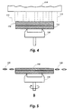
- Figure 4 shows an array 110 which overlaps a substrate 112 such that if all droplet ejectors eject droplets 113, a smooth, even coating of resist 114 is produced.
- the resist layer may be made sufficiently thin and well controlled that subsequent spin coating is not required.
- the substrate 112 can be attached to a rotating mount 116. If required, after deposition of the resist layer (as illustrated in Figure 4), the rotating mount 116 can be spun as shown in Figure 5 to produce a spin coated resist layer 118 from the resist 114. During spinning, small droplets 120 of excess resist are spun off.
- the advantage of the spin coating method illustrated in Figures 4 and 5 over the prior art is that, when using the principles of the present invention, the initial resist deposition can be made smooth and thin prior to spinning. This reduces the material waste, and consequently reduces the safety and environmental concerns over the prior art spin coating process. Additionally, if the initially deposited resist layer is thin, much smaller resist droplets are spun off the substrate, and thus less effort need be expended to prevent the spun off droplets from returning to the substrate.
- droplet ejection refers to the forcing of droplets from the surface of a material.
- droplet ejection frequently refers to causing a droplet to leave the surface of a material in such a way that the droplet travels along a particular path.
- the paths taken by the droplets are largely immaterial.
- mists are created which can be used to form material layers on substrates.
- RF pulses For example, by driving the transducers of an array of acoustic droplet ejectors with high intensity, but short duration RF pulses, mists are created which can be used to form material layers on substrates. See, Elrod et al., "Nozzleless droplet formation with focused acoustic beams," particularly pp. 3444, “VI. Pulse width: ejection stability and droplet diameter,” J. Appl. Phys. Vol. 65, 1 May 1989.
- Figure 6 shows a cross- sectional view of three sections, the sections 200 through 202, of polyimide deposited on a glass receptor 206.
- Each of the sections is a different color, such as red, blue, or green, and could be used as a color filter.
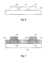
- Figure 7 shows a printed circuit board 300 having a plurality of coppertraces 302. Over the copper trace is deposited a protective urethane coating 304 which protects the copper traces 302.
- Figure 8 shows an even more complex three dimensional structure which is formed by repeated depositions.
- a variable thickness first metallic layer 400 say of solder
- Figure 8 also shows a polymer layer 404 which is selectively deposited over the first metallic layer 400.
- a second metallic layer 406 say again of solder.
- the various layers 400, 404, and 406 may be of the same material.
- the principles of the present invention can be applied to create three dimensional structures using a wide range of materials.
- acoustic droplet ejectors illustrated in Figures 1 and 2 are believed to be useful for a wide range of materials and droplet sizes.
- ZnO acoustic transducers become difficult to implement.
- Transducers made of alternative materials such as lithium niobate (LiNb0 3 ) or a piezoelectric polymer such as PVF 2 ,or PZT, are then beneficial.
- the droplet ejectors depicted in Figures 1and 2 pass the acoustic energy from the transducer through the base, this is not required.
- An alternative droplet ejector 498 which uses LiNb0 3 transducers and which does not pass the acoustic energy through a base is described below with the assistance of Figures 9 and 10.
- a planar surface acoustic transducer 500 which includes a piezoelectric plate 502 of LiN- b0 3 launches focused acoustic energy in a cone 503 through a material 504 that is to be ejected as droplets 506.
- the material 504 is held within a container 508 such that the free surface 510 of the material is at or is near the focus area of the acoustic energy.
- the acoustic transducer emits acoustic energy, that energy emits droplets from the free surface.
- the acoustic transducer 500 is comprised of the piezoelectric plate 502 and a pair of mulit-element, ring-shaped electrodes, the electrodes 512 and 514, which are generally concentrically deposited in an interdigitated relationship on the upper surface of the piezoelectric plate.
- an AC power supply 516 applies power to the electrodes 512 and 514, radially propagating, coherent Ray- leigh waves are piezoelectrically generated on the surface of the piezoelectric plate 502.
- the surface waves Due to the in- compressibility of the material 504 and the relatively low velocity of sound through the piezoelectric plate, the surface waves cause a generally circular pattern of coherent longitudinal acoustic energy to leak into the material 504 at predetermined acute angles with respect to the surface of the plate: i.e., the longitudinal acoustic energy is focused.
- Such ejectors are described in more detail in US-A-4,697,195.
Abstract
Description
- This invention relates to the deposition of material layers using acoustically ejected droplets.
- Modern fabrication processes frequently require depositions of layers of one or more materials onto a receptor. For example, most semiconductor fabrication processes require that a resist (such as photoresist or electron resist) be deposited on a substrate. Then by using photolithographic techniques, selected areas of the resist layer can be removed and the underlying substrate can be subjected to subsequent processing (such as metal film deposition) to form complex semiconductor devices.
- While semiconductor fabrication is an important fabrication process which requires the deposition of material layers, it is certainly not the only one. Other examples include the deposition of molten solder onto printed circuit boards, the deposition of catalysts, such as those used in the production of flex cables, and the deposition of materials, such as hot melt waxes, to create three dimensional structures.
- While some fabrication processes, such as creating three dimensional structures, require depositions of materials over controlled areas of a receptor, in other processes, such as semiconductor fabrication, the deposited layer can simply be uniformly formed over the entire surface of the receptor. While forming a uniform layer over the entire surface of a receptor is usually much simpler than depositing a layer over selected areas of a receptor, even the simpler case has its problems. The depositing of resist onto a substrate will illustrate some of those problems.
- Resist is usually applied to a substrate using a process called spin coating. A typical spin coating process begins with the placement of a relatively thick layer of liquid resist over the substrate. This may be accomplished by pouring liquid resist on the center of a slowly rotating substrate. As the substrate rotates, the resist spreads over the substrate. After the substrate is fully coated with the resist, the substrate is quickly accelerated, causing excess resist to flow over the substrate toward its edges. Finally, the substrate is rotated at high speed so that droplets of the excess resist are spun off of the substrate, leaving only a thin, even layer of resist. After the resist's solvent sufficiently evaporates, the resist is solid and the spinning stops.
- While spin coating is a highly developed process, it has the problem of being wasteful of resist since most of the resist is spun off the substrate. Another problem is the great care that must be taken to prevent the large droplets which are spun off of the substrate from returning to the substrate and disturbing the existing resist layer. A third problem is a result of the chemicals which comprise modern resists. Many of those chemicals are toxic and hazardous to both the health of workers and to the environment. Thus, the less resist used, the better. Additionally, spin coating cannot easily apply layers in selected locations of the substrate. This is a significant drawback since multilevel depositions (which are three dimensional structures)are not easily formed, if at all, using spin coating.
- In other applications in which a material is deposited over a wide area, such as in some color filter fabrication techniques, the deposited material is expensive. Techniques which reduce the amount of material that is deposited are beneficial.
- As previously mentioned, the difficulty of depositing material layers over selected areas of a receptor are greater then when simply fully coating a surface. For example, one cannot easily use spin coating. Furthermore, once a particular technique of depositing a layer over selected areas of a receptor is developed, any change in the area being covered may be difficult to implement.
- Therefore, a new method of depositing one or more material layers onto a receptor, particularly a method capable of saving material and which permits the deposition of material only on selected areas of the receptor, would be beneficial.
- Various printing technologies have been developed for marking recording media. For example, thermal inkjet printing operates by rapidly heating an element to cause ejection of a bubble from a nozzle. Another prior art printing technology is the piezoelectric inkjet. In a piezoelectric inkjet printer, an electric voltage causes a piezoelectric element in a liquid to expand, thereby forcing a droplet from a nozzle. It should be noted that nozzle based printers tend to clog. Another problem with nozzle based printers is the difficulty of obtaining large numbers of very small and accurately placed nozzles at reasonable cost. Because of this, nozzle based printers typically use a relatively small printhead which moves in a raster fashion across a recording medium.
- When printing, the primary goal is to deposit a marking fluid over predetermined areas of a recording medium. In contrast, when depositing uniform layers of materials on a receptor, the goal is to deposit a smooth, even layer of material at a predetermined thickness over a receptor.
- While there are many other printer technologies, of importance to the present invention is acoustic printing. In acoustic printing, focused acoustic energy ejects droplets from the free surface of a marking fluid onto a recording medium. More detailed descriptions of acoustic droplet ejection and acoustic printing in general are found in the following U.S. Patents and in their citations: 4,308,547; 4,697,195; 4,719,476; 4,719,480; 4,748,461; 4,751,529; 4,751,530; 4,751,534; 4,959,674; 5,028,937; 5,041,849; 5,087,931; 5,111,220; 5,121,141; 5,122,818; 5,142,307; and 5,216,451.
- It is to be noted that acoustic printers do not use nozzles, and are therefore unlikely to clog. Furthermore, acoustic printers can be fabricated using photolithographic techniques to have thousands of densely packed droplet ejectors, each of which ejects very small droplets.
- The present inventor has found that acoustic ejection of droplets of a wide variety of materials is possible. He also recognized that the high droplet ejector density and the small droplet sizes possible with acoustic printing technology can produce smooth, controlled layers of various materials on a receptor. Because of the relatively constant droplet dimensions from acoustic droplet ejectors, substantially uniform layers of predetermined thicknesses can be formed.
- In contrast, the tendency of nozzle based printing technologies to clog, combined with the relatively low density of droplet ejectors readily achievable, are believed to limit the utility of nozzle based printers for material layer formation.
- The present invention is a method of depositing material layers by acoustically ejecting droplets of the material onto a receptor until the desired layer is formed. Beneficially, the method relates to acoustic printing.
- The present invention provides a method of depositing a layer of material at a specified thickness on a receptor using an acoustic droplet ejector that ejects fluid using focused acoustic energy, the method comprising the steps of: orienting the acoustic droplet ejector and the receptor such that fluid ejected by the acoustic droplet ejector is deposited onto the receptor; and ejecting fluid using the acoustic droplet ejector until the specified material thickness is formed on the receptor.
- The invention further provides a method of fabricating a three-dimensional structure according to claim 4 of the appended claims.
- The invention further provides a method of depositing a resist layer onto a substrate, according to claim 9 of the appended claims.
- Other aspects of the present invention will become apparent as the following description proceeds and upon reference to the drawings, in which:
- Figure 1 is an unscaled view of a first embodiment of a single acoustic droplet ejector ejecting a droplet of resist;
- Figure 2 is an unscaled view of a second embodiment of a single acoustic droplet ejector ejecting a droplet of resist;
- Figure 3 is an unscaled view of an array of acoustic droplet ejectors, each according to Figures 1 or 2, depositing resist onto a substrate in a controlled fashion so as to form a layer in a predetermined pattern;
- Figure 4 is an unscaled view of an array of acoustic droplet ejectors ejecting resist onto a substrate;
- Figure 5 is an unscaled view of the resist and substrate in Figure 4 being spun to produce a thin, uniform coating of resist;
- Figure 6 is an unscaled, cut-away view of polyimide deposited on a glass substrate;
- Figure 7 is an unscaled, cut-away view of a three layer structure formed using the principles of the present invention; and
- Figure 8 is an unscaled, cut-away view of a complex three layer structure formed using the principles of the present invention;
- Figure 9 is a schematic depiction of an alternative embodiment droplet ejector; and
- Figure 10 is a top down view of the transducer/fo- cusing element of the acoustic droplet ejector of Figure 9.
- The principles of the present invention will become clearer after study of the commercially important embodiment of acoustically depositing a uniform layer of resist upon a substrate. Refer now to Figure 1 for an illustration of an exemplary
acoustic droplet ejector 10. Figure 1 shows thedroplet ejector 10 shortly after ejection of adroplet 12 of resist 14 and before themound 16 on thefree surface 18 of the resist 14 has relaxed. - The forming of the
mound 16 and the subsequent ejection of thedroplet 12 is the result of pressure exerted by acoustic forces created by aZnO transducer 20. To generate the acoustic pressure, RF drive energy is applied to theZnO transducer 20 from anRF driver source 22 via abottom electrode 24 and atop electrode 26. The acoustic energy from the transducer passes through a base 28 into anacoustic lens 30. The acoustic lens focuses its received acoustic energy into a small focal area which is at, or near, thefree surface 18 of the resist 14. Provided the energy of the acoustic beam is sufficient and properly focused relative to the free surface of the resist, amound 16 is formed and adroplet 12 is subsequently ejected. - Still referring to Figure 1, the acoustic energy from the
acoustic lens 30 passes through aliquid cell 32 filled with a liquid having a relatively low attenuation. The bottom of theliquid cell 32 is formed by thebase 28, the sides of the liquid cell are formed by surfaces of an aperture in atop plate 34, and the top of the liquid cell is sealed by an acousticallythin capping structure 36. By "acoustically thin" it is implied that the thickness of the capping structure is less than the wavelength of the applied acoustic energy. - The
droplet ejector 10 further includes areservoir 38, located over the cappingstructure 36, which holds resist 14. As shown in Figure 1, the reservoir includes anopening 40 defined by sidewalls 42. It should be noted that theopening 40 is axially aligned with theliquid cell 32. Theside walls 42 include a plurality ofportholes 44 through which the resist passes. A pressure means 46 forces resist 14 through theportholes 44 so as to create a pool of resist having thefree surface 18 over the cappingstructure 36. - The
droplet ejector 10 is dimensioned so that thefree surface 18 of the resist is at, or is near, the acoustic focal area. Since the cappingstructure 36 is acoustically thin, the acoustic energy readily passes through the capping structure and into the overlaying resist. - A droplet ejector similar to the
droplet ejector 10, including the acoustically thin capping structure and reservoir, is described in EP-A-572,241. - Asecond embodiment
acoustic droplet ejector 50 is illustrated in Figure 2. Thedroplet ejector 50 does not have aliquid cell 32 sealed by an acousticallythin capping structure 36 Nor does it have the reservoir filled with resist 14 or any of the elements associated with the reservoir (such as the pressure means). Rather, the acoustic energy passes from theacoustic lens 30 directly into resist 14. However,droplets 12 are still ejected frommounds 16 formed on thefree surface 18 of the resist. - While the
acoustic droplet ejector 50 is conceptually simpler than theacoustic droplet ejector 10, it should be noted that the longer path length through the resist of theacoustic droplet ejector 50 might result in excessive acoustic attenuation and require larger acoustic power for droplet ejection. - As with other acoustic droplet ejectors, droplet ejectors which form deposition layers can be reproduced many, perhaps thousands, of times using photolithographic techniques.
- Figure 3 shows an
array 100 ofindividual droplet ejectors 101, of which five are ejectingdroplets 12 of resist 14 onto asubstrate 102. Figure 3 illustrates an interesting application of acoustic deposition of materials: patterning. As in acoustic printing, individual ones or groups of droplet ejectors can be controlled so as to deposit predetermined patterned layers on a receptor. - While ejection from an array of individual droplet ejectors could be controlled as illustrated in Figure 3 (and as in acoustic printing) to create an "image" of resist on a substrate, in semiconductor fabrication this is not necessarily desirable. For example, Figure 4 shows an
array 110 which overlaps asubstrate 112 such that if all droplet ejectors ejectdroplets 113, a smooth, even coating of resist 114 is produced. - In some fabrication applications, the resist layer may be made sufficiently thin and well controlled that subsequent spin coating is not required. However, as shown in Figures 4 and 5, the
substrate 112 can be attached to arotating mount 116. If required, after deposition of the resist layer (as illustrated in Figure 4), therotating mount 116 can be spun as shown in Figure 5 to produce a spin coated resistlayer 118 from the resist 114. During spinning,small droplets 120 of excess resist are spun off. The advantage of the spin coating method illustrated in Figures 4 and 5 over the prior art is that, when using the principles of the present invention, the initial resist deposition can be made smooth and thin prior to spinning. This reduces the material waste, and consequently reduces the safety and environmental concerns over the prior art spin coating process. Additionally, if the initially deposited resist layer is thin, much smaller resist droplets are spun off the substrate, and thus less effort need be expended to prevent the spun off droplets from returning to the substrate. - The individual acoustic droplet ejectors described with reference to Figures 1 and 2, and their applications with regards to Figures 4 and 5, have been described as "ejecting" droplets. It is to be understood that droplet ejection as used herein refers to the forcing of droplets from the surface of a material. In other contexts, such as acoustic ink printing, droplet ejection frequently refers to causing a droplet to leave the surface of a material in such a way that the droplet travels along a particular path. The difference being that in some material deposition applications, such as resist depositions as described in relation to Figure 5, the paths taken by the droplets are largely immaterial. For example, by driving the transducers of an array of acoustic droplet ejectors with high intensity, but short duration RF pulses, mists are created which can be used to form material layers on substrates. See, Elrod et al., "Nozzleless droplet formation with focused acoustic beams," particularly pp. 3444, "VI. Pulse width: ejection stability and droplet diameter," J. Appl. Phys. Vol. 65, 1 May 1989.
- It is to be understood that the use of the present invention extends well beyond depositing resist on a substrate. For example, Figure 6 shows a cross- sectional view of three sections, the
sections 200 through 202, of polyimide deposited on aglass receptor 206. Each of the sections is a different color, such as red, blue, or green, and could be used as a color filter. - The present invention can also be used to create three dimensional structures. For example, Figure 7 shows a printed
circuit board 300 having a plurality ofcoppertraces 302. Over the copper trace is deposited aprotective urethane coating 304 which protects the copper traces 302. - Figure 8 shows an even more complex three dimensional structure which is formed by repeated depositions. First, a variable thickness first
metallic layer 400, say of solder, is deposited onto asubstrate 402. Note that, as shown in Figure 8, the principles of the present invention can be applied to create layers of nonconstant thickness. Figure 8 also shows apolymer layer 404 which is selectively deposited over the firstmetallic layer 400. On top of thepolymer layer 404 is deposited a secondmetallic layer 406, say again of solder. Of course, in other embodiments thevarious layers - The acoustic droplet ejectors illustrated in Figures 1 and 2 are believed to be useful for a wide range of materials and droplet sizes. However, at relatively low acoustic frequency (say 50 MHz), ZnO acoustic transducers become difficult to implement. Transducers made of alternative materials, such as lithium niobate (LiNb03) or a piezoelectric polymer such as PVF2,or PZT, are then beneficial. Further, while the droplet ejectors depicted in Figures 1and 2 pass the acoustic energy from the transducer through the base, this is not required. An
alternative droplet ejector 498 which uses LiNb03 transducers and which does not pass the acoustic energy through a base is described below with the assistance of Figures 9 and 10. - In Figure 9, a planar surface
acoustic transducer 500 which includes apiezoelectric plate 502 of LiN- b03 launches focused acoustic energy in acone 503 through a material 504 that is to be ejected asdroplets 506. Thematerial 504 is held within acontainer 508 such that thefree surface 510 of the material is at or is near the focus area of the acoustic energy. When the acoustic transducer emits acoustic energy, that energy emits droplets from the free surface. - Referring now to Figure 10, the
acoustic transducer 500 is comprised of thepiezoelectric plate 502 and a pair of mulit-element, ring-shaped electrodes, theelectrodes AC power supply 516 applies power to theelectrodes piezoelectric plate 502. Due to the in- compressibility of thematerial 504 and the relatively low velocity of sound through the piezoelectric plate, the surface waves cause a generally circular pattern of coherent longitudinal acoustic energy to leak into thematerial 504 at predetermined acute angles with respect to the surface of the plate: i.e., the longitudinal acoustic energy is focused. Such ejectors are described in more detail in US-A-4,697,195.
Claims (10)
Applications Claiming Priority (2)
| Application Number | Priority Date | Filing Date | Title |
|---|---|---|---|
| US24592294A | 1994-05-18 | 1994-05-18 | |
| US245922 | 1994-05-18 |
Publications (2)
| Publication Number | Publication Date |
|---|---|
| EP0682988A1 true EP0682988A1 (en) | 1995-11-22 |
| EP0682988B1 EP0682988B1 (en) | 2001-11-14 |
Family
ID=22928647
Family Applications (1)
| Application Number | Title | Priority Date | Filing Date |
|---|---|---|---|
| EP95303119A Expired - Lifetime EP0682988B1 (en) | 1994-05-18 | 1995-05-09 | Acoustic deposition of material layers |
Country Status (4)
| Country | Link |
|---|---|
| US (1) | US5591490A (en) |
| EP (1) | EP0682988B1 (en) |
| JP (1) | JPH07314664A (en) |
| DE (1) | DE69523815T2 (en) |
Cited By (4)
| Publication number | Priority date | Publication date | Assignee | Title |
|---|---|---|---|---|
| EP0919641A1 (en) * | 1997-11-25 | 1999-06-02 | Xerox Corporation | A method of manufacturing 3D parts using a sacrificial metal |
| EP0919640A1 (en) * | 1997-11-25 | 1999-06-02 | Xerox Corporation | A method of manufacturing three dimensional parts using an inert gas |
| US6007183A (en) * | 1997-11-25 | 1999-12-28 | Xerox Corporation | Acoustic metal jet fabrication using an inert gas |
| EP2232572A1 (en) * | 2007-12-07 | 2010-09-29 | Sunprint Inc. | Focused acoustic printing of patterned photovoltaic materials |
Families Citing this family (42)
| Publication number | Priority date | Publication date | Assignee | Title |
|---|---|---|---|---|
| DE69610863T2 (en) * | 1995-02-21 | 2001-06-07 | Toshiba Kawasaki Kk | Inkjet printer |
| JP2842320B2 (en) | 1995-08-22 | 1999-01-06 | 日本電気株式会社 | Droplet ejection device and droplet ejection method |
| JP2861980B2 (en) * | 1997-01-30 | 1999-02-24 | 日本電気株式会社 | Ink drop ejector |
| DE19806807A1 (en) | 1997-02-19 | 1998-09-03 | Nec Corp | Droplet ejection arrangement especially for ink jet recording head |
| US6003388A (en) * | 1997-09-17 | 1999-12-21 | The United States Of America As Represented By The Administrator Of The National Aeronautics And Space Administration | System for manipulating drops and bubbles using acoustic radiation pressure |
| US6086942A (en) | 1998-05-27 | 2000-07-11 | International Brachytherapy S.A. | Fluid-jet deposition of radioactive material for brachytherapy devices |
| US6364454B1 (en) | 1998-09-30 | 2002-04-02 | Xerox Corporation | Acoustic ink printing method and system for improving uniformity by manipulating nonlinear characteristics in the system |
| US6302524B1 (en) | 1998-10-13 | 2001-10-16 | Xerox Corporation | Liquid level control in an acoustic droplet emitter |
| US6753922B1 (en) * | 1998-10-13 | 2004-06-22 | Intel Corporation | Image sensor mounted by mass reflow |
| US6136210A (en) * | 1998-11-02 | 2000-10-24 | Xerox Corporation | Photoetching of acoustic lenses for acoustic ink printing |
| US6416678B1 (en) | 1998-12-22 | 2002-07-09 | Xerox Corporation | Solid bi-layer structures for use with high viscosity inks in acoustic ink printing and methods of fabrication |
| US6134291A (en) * | 1999-07-23 | 2000-10-17 | Xerox Corporation | Acoustic ink jet printhead design and method of operation utilizing flowing coolant and an emission fluid |
| US6154236A (en) * | 1999-07-23 | 2000-11-28 | Xerox Corporation | Acoustic ink jet printhead design and method of operation utilizing flowing coolant and an emission fluid |
| US6422684B1 (en) | 1999-12-10 | 2002-07-23 | Sensant Corporation | Resonant cavity droplet ejector with localized ultrasonic excitation and method of making same |
| US6808934B2 (en) | 2000-09-25 | 2004-10-26 | Picoliter Inc. | High-throughput biomolecular crystallization and biomolecular crystal screening |
| US6746104B2 (en) | 2000-09-25 | 2004-06-08 | Picoliter Inc. | Method for generating molecular arrays on porous surfaces |
| US6666541B2 (en) | 2000-09-25 | 2003-12-23 | Picoliter Inc. | Acoustic ejection of fluids from a plurality of reservoirs |
| US6642061B2 (en) | 2000-09-25 | 2003-11-04 | Picoliter Inc. | Use of immiscible fluids in droplet ejection through application of focused acoustic energy |
| EP1324823B1 (en) | 2000-09-25 | 2007-12-26 | Picoliter, Inc. | Focused acoustic energy in the preparation and screening of combinatorial libraries |
| US20020037359A1 (en) * | 2000-09-25 | 2002-03-28 | Mutz Mitchell W. | Focused acoustic energy in the preparation of peptide arrays |
| US6548308B2 (en) | 2000-09-25 | 2003-04-15 | Picoliter Inc. | Focused acoustic energy method and device for generating droplets of immiscible fluids |
| US6596239B2 (en) * | 2000-12-12 | 2003-07-22 | Edc Biosystems, Inc. | Acoustically mediated fluid transfer methods and uses thereof |
| US6464337B2 (en) * | 2001-01-31 | 2002-10-15 | Xerox Corporation | Apparatus and method for acoustic ink printing using a bilayer printhead configuration |
| US6869551B2 (en) * | 2001-03-30 | 2005-03-22 | Picoliter Inc. | Precipitation of solid particles from droplets formed using focused acoustic energy |
| US6872320B2 (en) * | 2001-04-19 | 2005-03-29 | Xerox Corporation | Method for printing etch masks using phase-change materials |
| US6742884B2 (en) * | 2001-04-19 | 2004-06-01 | Xerox Corporation | Apparatus for printing etch masks using phase-change materials |
| US6533380B1 (en) | 2001-09-12 | 2003-03-18 | Xerox Corporation | Method and apparatus for reducing neighbor cross-talk and increasing robustness of an acoustic printing system against isolated ejector failure |
| US6976639B2 (en) | 2001-10-29 | 2005-12-20 | Edc Biosystems, Inc. | Apparatus and method for droplet steering |
| US6925856B1 (en) | 2001-11-07 | 2005-08-09 | Edc Biosystems, Inc. | Non-contact techniques for measuring viscosity and surface tension information of a liquid |
| US7354141B2 (en) * | 2001-12-04 | 2008-04-08 | Labcyte Inc. | Acoustic assessment of characteristics of a fluid relevant to acoustic ejection |
| US6972261B2 (en) * | 2002-06-27 | 2005-12-06 | Xerox Corporation | Method for fabricating fine features by jet-printing and surface treatment |
| US7275807B2 (en) * | 2002-11-27 | 2007-10-02 | Edc Biosystems, Inc. | Wave guide with isolated coupling interface |
| US7429359B2 (en) * | 2002-12-19 | 2008-09-30 | Edc Biosystems, Inc. | Source and target management system for high throughput transfer of liquids |
| US6827287B2 (en) * | 2002-12-24 | 2004-12-07 | Palo Alto Research Center, Incorporated | High throughput method and apparatus for introducing biological samples into analytical instruments |
| US7976891B1 (en) * | 2005-12-16 | 2011-07-12 | Advanced Cardiovascular Systems, Inc. | Abluminal stent coating apparatus and method of using focused acoustic energy |
| US7753636B2 (en) * | 2008-03-25 | 2010-07-13 | Hennig Emmett D | Adjustable bale mover spikes |
| US8282999B2 (en) * | 2008-04-04 | 2012-10-09 | Micron Technology, Inc. | Spin-on film processing using acoustic radiation pressure |
| DE102008057121A1 (en) | 2008-11-13 | 2009-06-25 | Daimler Ag | Method for coating component and/or substrate with fluid medium i.e. colored paint, involves mechanically and/or acoustically exciting component and/or substrate and/or fluid medium during coating process and/or immediately after process |
| DE102008057120A1 (en) | 2008-11-13 | 2009-06-25 | Daimler Ag | Method for coating component and/or substrate with fluid medium i.e. colored paint, involves mechanically and/or acoustically activating component and/or substrate for drying after coating process by ultrasound |
| US20100184244A1 (en) * | 2009-01-20 | 2010-07-22 | SunPrint, Inc. | Systems and methods for depositing patterned materials for solar panel production |
| JP6869673B2 (en) * | 2016-09-15 | 2021-05-12 | 東芝テック株式会社 | Inkjet head |
| DE102019102232A1 (en) * | 2018-01-30 | 2019-08-01 | Ford Motor Company | ULTRASONIC TRANSMITTER WITH ACOUSTIC FOCUSING DEVICE |
Citations (9)
| Publication number | Priority date | Publication date | Assignee | Title |
|---|---|---|---|---|
| US3198170A (en) * | 1961-03-11 | 1965-08-03 | Copal Co Ltd | Ultrasonic-wave painting machine |
| CH512266A (en) * | 1969-08-07 | 1971-09-15 | Cosmeca Ag | Device for applying metal layers to a workpiece |
| JPS59211571A (en) * | 1983-05-18 | 1984-11-30 | Hitachi Ltd | Metallizing method |
| JPS62185322A (en) * | 1986-02-10 | 1987-08-13 | Nec Corp | Applicator for photo-resist |
| JPS6314848A (en) * | 1986-07-08 | 1988-01-22 | Nippon Steel Corp | Method for coating material onto steel sheet |
| WO1988007704A1 (en) * | 1987-04-03 | 1988-10-06 | Macdermid, Incorporated | Thermal stabilization of photoresist images |
| WO1990011837A1 (en) * | 1989-04-05 | 1990-10-18 | Olin Hunt Specialty Products Inc. | Process for coating a photoresist composition onto a substrate |
| JPH03107471A (en) * | 1989-09-22 | 1991-05-07 | Nkk Corp | Method for plating metallic strip with molten metal |
| JPH05282934A (en) * | 1992-03-31 | 1993-10-29 | Kyocera Corp | Formation of transparent conductive film |
Family Cites Families (24)
| Publication number | Priority date | Publication date | Assignee | Title |
|---|---|---|---|---|
| US4308547A (en) * | 1978-04-13 | 1981-12-29 | Recognition Equipment Incorporated | Liquid drop emitter |
| US4290384A (en) * | 1979-10-18 | 1981-09-22 | The Perkin-Elmer Corporation | Coating apparatus |
| US4697195A (en) * | 1985-09-16 | 1987-09-29 | Xerox Corporation | Nozzleless liquid droplet ejectors |
| US4748461A (en) * | 1986-01-21 | 1988-05-31 | Xerox Corporation | Capillary wave controllers for nozzleless droplet ejectors |
| US4719480A (en) * | 1986-04-17 | 1988-01-12 | Xerox Corporation | Spatial stablization of standing capillary surface waves |
| US4719476A (en) * | 1986-04-17 | 1988-01-12 | Xerox Corporation | Spatially addressing capillary wave droplet ejectors and the like |
| US4751534A (en) * | 1986-12-19 | 1988-06-14 | Xerox Corporation | Planarized printheads for acoustic printing |
| US4751529A (en) * | 1986-12-19 | 1988-06-14 | Xerox Corporation | Microlenses for acoustic printing |
| US4751530A (en) * | 1986-12-19 | 1988-06-14 | Xerox Corporation | Acoustic lens arrays for ink printing |
| US4797693A (en) * | 1987-06-02 | 1989-01-10 | Xerox Corporation | Polychromatic acoustic ink printing |
| US4845517A (en) * | 1988-01-11 | 1989-07-04 | Am International, Inc. | Droplet deposition apparatus |
| US5122818A (en) * | 1988-12-21 | 1992-06-16 | Xerox Corporation | Acoustic ink printers having reduced focusing sensitivity |
| JPH02185322A (en) * | 1989-01-06 | 1990-07-19 | Mitsubishi Electric Corp | Electric discharge machining device |
| US5028937A (en) * | 1989-05-30 | 1991-07-02 | Xerox Corporation | Perforated membranes for liquid contronlin acoustic ink printing |
| JPH0649801B2 (en) * | 1989-06-12 | 1994-06-29 | 東海カーボン株式会社 | Carbon black for compounding functional parts rubber |
| US4959674A (en) * | 1989-10-03 | 1990-09-25 | Xerox Corporation | Acoustic ink printhead having reflection coating for improved ink drop ejection control |
| US5041849A (en) * | 1989-12-26 | 1991-08-20 | Xerox Corporation | Multi-discrete-phase Fresnel acoustic lenses and their application to acoustic ink printing |
| US5087931A (en) * | 1990-05-15 | 1992-02-11 | Xerox Corporation | Pressure-equalized ink transport system for acoustic ink printers |
| US5040003A (en) * | 1990-06-04 | 1991-08-13 | Eastman Kodak Company | Method and apparatus for recording color with plural printheads |
| US5142307A (en) * | 1990-12-26 | 1992-08-25 | Xerox Corporation | Variable orifice capillary wave printer |
| US5121141A (en) * | 1991-01-14 | 1992-06-09 | Xerox Corporation | Acoustic ink printhead with integrated liquid level control layer |
| US5111220A (en) * | 1991-01-14 | 1992-05-05 | Xerox Corporation | Fabrication of integrated acoustic ink printhead with liquid level control and device thereof |
| US5216451A (en) * | 1992-12-27 | 1993-06-01 | Xerox Corporation | Surface ripple wave diffusion in apertured free ink surface level controllers for acoustic ink printers |
| JPH09211571A (en) * | 1996-01-30 | 1997-08-15 | Minolta Co Ltd | Pop-up type flashing device for camera |
-
1995
- 1995-05-09 EP EP95303119A patent/EP0682988B1/en not_active Expired - Lifetime
- 1995-05-09 DE DE69523815T patent/DE69523815T2/en not_active Expired - Lifetime
- 1995-05-16 JP JP7116782A patent/JPH07314664A/en active Pending
- 1995-11-13 US US08/556,672 patent/US5591490A/en not_active Expired - Lifetime
Patent Citations (9)
| Publication number | Priority date | Publication date | Assignee | Title |
|---|---|---|---|---|
| US3198170A (en) * | 1961-03-11 | 1965-08-03 | Copal Co Ltd | Ultrasonic-wave painting machine |
| CH512266A (en) * | 1969-08-07 | 1971-09-15 | Cosmeca Ag | Device for applying metal layers to a workpiece |
| JPS59211571A (en) * | 1983-05-18 | 1984-11-30 | Hitachi Ltd | Metallizing method |
| JPS62185322A (en) * | 1986-02-10 | 1987-08-13 | Nec Corp | Applicator for photo-resist |
| JPS6314848A (en) * | 1986-07-08 | 1988-01-22 | Nippon Steel Corp | Method for coating material onto steel sheet |
| WO1988007704A1 (en) * | 1987-04-03 | 1988-10-06 | Macdermid, Incorporated | Thermal stabilization of photoresist images |
| WO1990011837A1 (en) * | 1989-04-05 | 1990-10-18 | Olin Hunt Specialty Products Inc. | Process for coating a photoresist composition onto a substrate |
| JPH03107471A (en) * | 1989-09-22 | 1991-05-07 | Nkk Corp | Method for plating metallic strip with molten metal |
| JPH05282934A (en) * | 1992-03-31 | 1993-10-29 | Kyocera Corp | Formation of transparent conductive film |
Non-Patent Citations (5)
| Title |
|---|
| PATENT ABSTRACTS OF JAPAN vol. 009, no. 078 (C - 274) 6 April 1985 (1985-04-06) * |
| PATENT ABSTRACTS OF JAPAN vol. 012, no. 026 (E - 577) 26 January 1988 (1988-01-26) * |
| PATENT ABSTRACTS OF JAPAN vol. 012, no. 219 (C - 506) 22 June 1988 (1988-06-22) * |
| PATENT ABSTRACTS OF JAPAN vol. 015, no. 293 (C - 0853) 25 July 1991 (1991-07-25) * |
| PATENT ABSTRACTS OF JAPAN vol. 018, no. 063 (E - 1500) 2 February 1994 (1994-02-02) * |
Cited By (6)
| Publication number | Priority date | Publication date | Assignee | Title |
|---|---|---|---|---|
| EP0919641A1 (en) * | 1997-11-25 | 1999-06-02 | Xerox Corporation | A method of manufacturing 3D parts using a sacrificial metal |
| EP0919640A1 (en) * | 1997-11-25 | 1999-06-02 | Xerox Corporation | A method of manufacturing three dimensional parts using an inert gas |
| US6007183A (en) * | 1997-11-25 | 1999-12-28 | Xerox Corporation | Acoustic metal jet fabrication using an inert gas |
| US6019814A (en) * | 1997-11-25 | 2000-02-01 | Xerox Corporation | Method of manufacturing 3D parts using a sacrificial material |
| EP2232572A1 (en) * | 2007-12-07 | 2010-09-29 | Sunprint Inc. | Focused acoustic printing of patterned photovoltaic materials |
| EP2232572A4 (en) * | 2007-12-07 | 2012-10-17 | Alion Inc | Focused acoustic printing of patterned photovoltaic materials |
Also Published As
| Publication number | Publication date |
|---|---|
| DE69523815T2 (en) | 2002-04-18 |
| DE69523815D1 (en) | 2001-12-20 |
| US5591490A (en) | 1997-01-07 |
| JPH07314664A (en) | 1995-12-05 |
| EP0682988B1 (en) | 2001-11-14 |
Similar Documents
| Publication | Publication Date | Title |
|---|---|---|
| EP0682988B1 (en) | Acoustic deposition of material layers | |
| US5565113A (en) | Lithographically defined ejection units | |
| US5631678A (en) | Acoustic printheads with optical alignment | |
| DE69928549T2 (en) | On-demand inkjet printing device, printing method and manufacturing method | |
| US4752787A (en) | Liquid jet recording head | |
| JP2006192622A (en) | Liquid-delivering head, liquid-delivering apparatus, and method for manufacturing liquid-delivering head | |
| JP2006224624A (en) | Laminated nozzle plate, liquid droplet discharge head and method for manufacturing laminated nozzle plate | |
| US20020062563A1 (en) | Method for processing discharge port of ink jet head, and method for manufacturing ink jet head | |
| RU2337828C2 (en) | Device for depositing drops | |
| JPH0952371A (en) | Ink jet head and production thereof | |
| EP0683405A1 (en) | Acoustic fabrication of color filters | |
| CA2281361C (en) | Liquid level control in an acoustic droplet emitter | |
| JP2000015820A (en) | Manufacture of orifice plate and liquid discharge head | |
| JP2006051640A (en) | Inkjet recording head and its manufacturing method | |
| US6076918A (en) | Method of manufacturing an electrostatic ink jet printing head with pointed ink ejectors | |
| EP1693204A2 (en) | Liquid droplet jetting apparatus and nozzle plate used in the same | |
| JPH05318732A (en) | Ink jet recording head | |
| JPH05124208A (en) | Liquid jet recording head and production thereof | |
| JPH05330061A (en) | Production of liquid droplet jet device | |
| JP2003311973A (en) | Liquid discharge device, printer, and manufacturing method for liquid discharge device | |
| JPS634955A (en) | Liquid jet recording head | |
| JP3032282B2 (en) | Droplet ejection recording device | |
| JPH05261925A (en) | Ink jet recording method and recording head | |
| JP2713786B2 (en) | Method for manufacturing liquid jet recording head | |
| JPH04191052A (en) | Manufacture of liquid jet record head |
Legal Events
| Date | Code | Title | Description |
|---|---|---|---|
| PUAI | Public reference made under article 153(3) epc to a published international application that has entered the european phase |
Free format text: ORIGINAL CODE: 0009012 |
|
| AK | Designated contracting states |
Kind code of ref document: A1 Designated state(s): DE FR GB |
|
| 17P | Request for examination filed |
Effective date: 19960522 |
|
| 17Q | First examination report despatched |
Effective date: 19980511 |
|
| GRAG | Despatch of communication of intention to grant |
Free format text: ORIGINAL CODE: EPIDOS AGRA |
|
| GRAG | Despatch of communication of intention to grant |
Free format text: ORIGINAL CODE: EPIDOS AGRA |
|
| GRAH | Despatch of communication of intention to grant a patent |
Free format text: ORIGINAL CODE: EPIDOS IGRA |
|
| GRAH | Despatch of communication of intention to grant a patent |
Free format text: ORIGINAL CODE: EPIDOS IGRA |
|
| GRAA | (expected) grant |
Free format text: ORIGINAL CODE: 0009210 |
|
| STAA | Information on the status of an ep patent application or granted ep patent |
Free format text: STATUS: THE PATENT HAS BEEN GRANTED |
|
| AK | Designated contracting states |
Kind code of ref document: B1 Designated state(s): DE FR GB |
|
| REF | Corresponds to: |
Ref document number: 69523815 Country of ref document: DE Date of ref document: 20011220 |
|
| REG | Reference to a national code |
Ref country code: GB Ref legal event code: IF02 |
|
| PLBE | No opposition filed within time limit |
Free format text: ORIGINAL CODE: 0009261 |
|
| 26N | No opposition filed | ||
| PGFP | Annual fee paid to national office [announced via postgrant information from national office to epo] |
Ref country code: GB Payment date: 20140425 Year of fee payment: 20 |
|
| PGFP | Annual fee paid to national office [announced via postgrant information from national office to epo] |
Ref country code: DE Payment date: 20140424 Year of fee payment: 20 |
|
| PGFP | Annual fee paid to national office [announced via postgrant information from national office to epo] |
Ref country code: FR Payment date: 20140521 Year of fee payment: 20 |
|
| REG | Reference to a national code |
Ref country code: DE Ref legal event code: R071 Ref document number: 69523815 Country of ref document: DE |
|
| REG | Reference to a national code |
Ref country code: GB Ref legal event code: PE20 Expiry date: 20150508 |
|
| PG25 | Lapsed in a contracting state [announced via postgrant information from national office to epo] |
Ref country code: GB Free format text: LAPSE BECAUSE OF EXPIRATION OF PROTECTION Effective date: 20150508 |