EP0689143A1 - Data storage subsystem - Google Patents
Data storage subsystem Download PDFInfo
- Publication number
- EP0689143A1 EP0689143A1 EP95304182A EP95304182A EP0689143A1 EP 0689143 A1 EP0689143 A1 EP 0689143A1 EP 95304182 A EP95304182 A EP 95304182A EP 95304182 A EP95304182 A EP 95304182A EP 0689143 A1 EP0689143 A1 EP 0689143A1
- Authority
- EP
- European Patent Office
- Prior art keywords
- storage device
- data
- controller
- device controller
- storage
- Prior art date
- Legal status (The legal status is an assumption and is not a legal conclusion. Google has not performed a legal analysis and makes no representation as to the accuracy of the status listed.)
- Withdrawn
Links
Images


Classifications
-
- G—PHYSICS
- G06—COMPUTING; CALCULATING OR COUNTING
- G06F—ELECTRIC DIGITAL DATA PROCESSING
- G06F11/00—Error detection; Error correction; Monitoring
- G06F11/07—Responding to the occurrence of a fault, e.g. fault tolerance
- G06F11/16—Error detection or correction of the data by redundancy in hardware
- G06F11/20—Error detection or correction of the data by redundancy in hardware using active fault-masking, e.g. by switching out faulty elements or by switching in spare elements
- G06F11/2053—Error detection or correction of the data by redundancy in hardware using active fault-masking, e.g. by switching out faulty elements or by switching in spare elements where persistent mass storage functionality or persistent mass storage control functionality is redundant
- G06F11/2056—Error detection or correction of the data by redundancy in hardware using active fault-masking, e.g. by switching out faulty elements or by switching in spare elements where persistent mass storage functionality or persistent mass storage control functionality is redundant by mirroring
- G06F11/2087—Error detection or correction of the data by redundancy in hardware using active fault-masking, e.g. by switching out faulty elements or by switching in spare elements where persistent mass storage functionality or persistent mass storage control functionality is redundant by mirroring with a common controller
-
- G—PHYSICS
- G06—COMPUTING; CALCULATING OR COUNTING
- G06F—ELECTRIC DIGITAL DATA PROCESSING
- G06F12/00—Accessing, addressing or allocating within memory systems or architectures
- G06F12/02—Addressing or allocation; Relocation
- G06F12/08—Addressing or allocation; Relocation in hierarchically structured memory systems, e.g. virtual memory systems
- G06F12/0802—Addressing of a memory level in which the access to the desired data or data block requires associative addressing means, e.g. caches
- G06F12/0866—Addressing of a memory level in which the access to the desired data or data block requires associative addressing means, e.g. caches for peripheral storage systems, e.g. disk cache
-
- G—PHYSICS
- G06—COMPUTING; CALCULATING OR COUNTING
- G06F—ELECTRIC DIGITAL DATA PROCESSING
- G06F3/00—Input arrangements for transferring data to be processed into a form capable of being handled by the computer; Output arrangements for transferring data from processing unit to output unit, e.g. interface arrangements
- G06F3/06—Digital input from, or digital output to, record carriers, e.g. RAID, emulated record carriers or networked record carriers
- G06F3/0601—Interfaces specially adapted for storage systems
-
- G—PHYSICS
- G11—INFORMATION STORAGE
- G11C—STATIC STORES
- G11C29/00—Checking stores for correct operation ; Subsequent repair; Testing stores during standby or offline operation
- G11C29/70—Masking faults in memories by using spares or by reconfiguring
- G11C29/88—Masking faults in memories by using spares or by reconfiguring with partially good memories
-
- G—PHYSICS
- G06—COMPUTING; CALCULATING OR COUNTING
- G06F—ELECTRIC DIGITAL DATA PROCESSING
- G06F11/00—Error detection; Error correction; Monitoring
- G06F11/07—Responding to the occurrence of a fault, e.g. fault tolerance
- G06F11/08—Error detection or correction by redundancy in data representation, e.g. by using checking codes
- G06F11/10—Adding special bits or symbols to the coded information, e.g. parity check, casting out 9's or 11's
- G06F11/1008—Adding special bits or symbols to the coded information, e.g. parity check, casting out 9's or 11's in individual solid state devices
-
- G—PHYSICS
- G06—COMPUTING; CALCULATING OR COUNTING
- G06F—ELECTRIC DIGITAL DATA PROCESSING
- G06F11/00—Error detection; Error correction; Monitoring
- G06F11/07—Responding to the occurrence of a fault, e.g. fault tolerance
- G06F11/16—Error detection or correction of the data by redundancy in hardware
- G06F11/20—Error detection or correction of the data by redundancy in hardware using active fault-masking, e.g. by switching out faulty elements or by switching in spare elements
- G06F11/2053—Error detection or correction of the data by redundancy in hardware using active fault-masking, e.g. by switching out faulty elements or by switching in spare elements where persistent mass storage functionality or persistent mass storage control functionality is redundant
- G06F11/2056—Error detection or correction of the data by redundancy in hardware using active fault-masking, e.g. by switching out faulty elements or by switching in spare elements where persistent mass storage functionality or persistent mass storage control functionality is redundant by mirroring
- G06F11/2066—Optimisation of the communication load
-
- G—PHYSICS
- G06—COMPUTING; CALCULATING OR COUNTING
- G06F—ELECTRIC DIGITAL DATA PROCESSING
- G06F12/00—Accessing, addressing or allocating within memory systems or architectures
- G06F12/02—Addressing or allocation; Relocation
- G06F12/08—Addressing or allocation; Relocation in hierarchically structured memory systems, e.g. virtual memory systems
- G06F12/0802—Addressing of a memory level in which the access to the desired data or data block requires associative addressing means, e.g. caches
- G06F12/0844—Multiple simultaneous or quasi-simultaneous cache accessing
- G06F12/0853—Cache with multiport tag or data arrays
-
- G—PHYSICS
- G06—COMPUTING; CALCULATING OR COUNTING
- G06F—ELECTRIC DIGITAL DATA PROCESSING
- G06F3/00—Input arrangements for transferring data to be processed into a form capable of being handled by the computer; Output arrangements for transferring data from processing unit to output unit, e.g. interface arrangements
- G06F3/06—Digital input from, or digital output to, record carriers, e.g. RAID, emulated record carriers or networked record carriers
- G06F3/0601—Interfaces specially adapted for storage systems
- G06F3/0668—Interfaces specially adapted for storage systems adopting a particular infrastructure
- G06F3/0671—In-line storage system
- G06F3/0673—Single storage device
-
- G—PHYSICS
- G11—INFORMATION STORAGE
- G11C—STATIC STORES
- G11C29/00—Checking stores for correct operation ; Subsequent repair; Testing stores during standby or offline operation
- G11C29/70—Masking faults in memories by using spares or by reconfiguring
- G11C29/74—Masking faults in memories by using spares or by reconfiguring using duplex memories, i.e. using dual copies
Definitions
- the present invention relates in general to an improved data storage subsystem and in particular to a fault tolerant data storage subsystem suitable for utilization within a data processing system.
- a typical data processing system generally includes one or more memory units which are connected to a central processor unit either directly or indirectly through a control unit and a channel.
- the function of these memory units is to store data and programs which are utilized by the central processing unit in performing a given data processing task.
- Various types of memory units are utilized in current data processing systems.
- the response time and capacities of these different memory types vary significantly, and in order to maximize system throughput the choice of a particular type of memory unit generally involves matching its response time to the requirement of the central processing unit and its capacity to the data storage needs of the data processing system.
- many data processing systems employ a number of different types of memory units. Since access time and capacity also affect the cost of storage, a typical system may include a fast access small capacity directly accessible monolithic memory for data that is utilized frequently and a series of tape memory devices or disk memory devices which are connected to the system through respective control units for data which is utilized less frequently.
- the storage capacities of these later units are generally several orders of magnitude greater than the semiconductor memories utilized within data processing systems and hence, the storage cost per byte of data is considerably less.
- Computer systems are currently being developed in which the amount of data to be manipulated by the system is immense.
- data storage systems have been proposed that are capable of handling amounts of data on the order of exabytes, spread across hundreds of direct access storage devices (DASD).
- Individual files for such systems have been proposed to be as high as ten gigabytes.
- Such large storage systems should be very reliable since restoring an entire storage system after a fault could take many hours or days.
- such storage systems should sustain very high data transfer rates in order to permit efficient utilization of the data.
- the prior art has suggested several techniques for solving this problem.
- the most straightforward approach provides the utilization of a duplicate set of storage devices or memory units which keep a duplicate file of all data. While this solution solves the data reliability problem this solution involves duplicating the cost of storage and some impact on system performance occurs since any change to stored data requires writing two records. Also, an added requirement of keeping track of where the duplicate records are kept is needed, in the event the primary records are not available.
- ECC Error Correction Codes
- RAID redundant arrays of inexpensive disks
- Such arrays offer the opportunity to achieve high data reliability at a lower cost than conventional methods which are based upon complete duplication of data.
- Various configurations of disk arrays have been proposed utilizing RAID technology and such systems typically provide high data reliability and availability.
- High data reliability means that the expected time to data loss is very long and the high availability of such systems means that the time spent repairing systems and recovering lost data is a small fraction of total time. While these arrays of disks provide enhanced data reliability, such systems are still prone to data loss in the event an error or fault occurs which is of sufficient magnitude to interrupt the recovery of data.
- the present invention provides a data storage subsystem comprising: a plurality of storage device controllers adapted to emulate a storage device, each storage device controller having a cache memory which includes multiple data input ports, multiple data output ports and at least one processing element for selectively interconnecting a selected data input port with a selected data output port within said cache memory; an interconnection for coupling a data output port of said cache memory within a first storage device controller with a data input port of said cache memory within a second storage device controller; and a first storage device selectively coupled to a data output port of said cache memory within said second storage device controller wherein a multipath dynamically alterable hierarchical arrangement of storage device controllers is established.
- multiple storage device controllers are provided which are each adaptable to emulate a storage device and which each include a cache memory which has multiple data input ports multiple data output ports.
- a processing element within the storage device controller is utilized to selectively interconnect particular data input ports with selected data output ports to provide multiple paths within the storage device controller.
- An interconnection is then provided for coupling a data output port of one storage device controller with a data input port of one or more alternate storage device controllers which emulate storage devices, creating an alterable hierarchical arrangement of storage device controllers.
- Storage devices are then coupled to each of the lowest levels of the hierarchical arrangement of storage device controllers. As the storage device controllers may vary in type and capability, various combinations of access speed and redundancy may be provided.
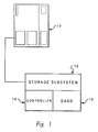
- the data processing system includes a host processor 10 which may be implemented utilizing any suitable computer such as, for example, the International Business Machines AS/400 computer. Additionally, a storage subsystem 12 is shown coupled to host processor 10 . As is common in such storage subsystems a controller 14 and one or more direct access storage devices 16 are also illustrated within storage subsystem 12 . Thus, in a manner which will be apparent to those having ordinary skill in the art, data utilized by host processor 10 may be stored and retrieved from one or more direct access storage devices within storage subsystem 12 .
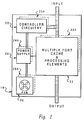
- storage device controller 14 includes controller circuitry 20 and a multiple port cache with processing elements 22 .
- An input to storage device controller 14 is provided for receiving data and, in combination with storage device controller 14 , multiple port cache and processing elements 22 may be utilized to emulate a storage device.
- storage device controller 14 may be coupled to a host processor and utilized to provide control of the storage of data within multiple disk memory devices in a manner transparent to the host processor.
- power supply 24 and backup power supply 24A are also depicted within Figure 2 .
- power supply 24 and backup power supply 24A are also depicted within Figure 2 .
- Those skilled in the art will appreciate that the provision of redundant power supplies which are controlled utilizing controller circuitry 20 can provide for a higher degree of reliability for the system in that the failure of a primary power supply will become transparent to the system as a result of the ability of storage controller 14 to seamlessly switch to backup power supply 24A .
- cooling fan 26 is depicted along with backup cooling fan 26A .
- these redundant cooling fan systems may be utilized to ensure that the failure of a cooling fan will not result in the loss of storage device controller 14 due to an overheating condition.
- backup controller circuitry 20A and backup multiple port cache 22A are also schematically illustrated within Figure 2 . In this manner, a catastrophic failure of any element within storage device controller 14 may be overcome by switching to a backup. Each of these backup switching techniques may be accomplished in a manner well known in the art.
- FIG. 2 In the manner depicted within Figure 2 , those skilled in the art will appreciate that it is possible to provide a storage device controller having multiple redundant subsystems and a multiple port cache and processing elements which is capable of emulating a disk memory device.
- the storage device controller of Figure 2 may be implemented utilizing the International Business Machines Corporation 3990 Storage Control Unit. Both the Model 3 and Model 6 3990 Storage Control Unit provide a multiple port cache and processing elements in the manner set forth within Figure 2 .
- FIG. 3 there is depicted a schematic representation of a multipath dynamically alterable hierarchical arrangement of storage device controllers which may be implemented utilizing the storage device controller of Figure 2 .
- a storage device controller 14 is coupled to multiple host processor 10 over multiple channels.
- multiple redundant subsystems of Figure 2 are not depicted in Figure 3 .
- multiple host processors may be coupled to storage device controller 14 utilizing a plurality of channels and simple contention resolution techniques may be utilized to determine which host processor is permitted to access storage device controller 14 at a single moment in time.
- Each processing element 30 preferably comprises a processor and selected control logic to permit data coupled to an input port 32 of multiple port cache 22 to be selectively coupled to one of multiple output ports 34 of an individual processing element 30 .
- selected output ports 34 of the processing elements 30 within storage device controller 14 are coupled to input ports 32 of a second group of storage device controllers 40 .
- storage device controller 14 may write data via processing elements 30 contained therein into the input ports 32 of storage device controllers 40 in the manner depicted.
- storage device controllers 40 which are coupled to the output ports of storage device controller 14 , may be said to implement a "virtual" storage device for purposes of illustration herein. In this manner, a highly reliable multipath dynamically alterable hierarchical arrangement of storage device controllers may be provided.
- a pair of disk arrays 42 which each include multiple disk memory devices 44 may then be coupled to the output ports 34 of storage device controllers 40 .
- storage device controllers 40 may be coupled to the output ports 34 of storage device controllers 40 .
- Various combinations of different types and capabilities of storage device controllers may be utilized to implement a desired spectrum of data reliability and access speed.
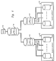
- FIG. 4 there is depicted a schematic representation of one embodiment of such a combination of storage device controllers in a multipath dynamically alterable hierarchical arrangement which includes various controller types.
- a host processor 10 is coupled to a storage device controller 14 which implements a RAID 1 type controller.
- storage device controller 14 implementing a RAID 1 type controller, will appear as a virtual storage device to host processor 10 .
- a RAID 1 controller implements the simplest approach to data reliability.
- a RAID 1 controller utilizes so-called "mirrored" disks in which data written to the controller is duplicated within two disk storage devices. This approach is fairly common in systems which utilize extremely valuable data. However, such systems require that each data write be applied to both disks within a pair. Also, since the data is duplicated within the mirrored disks, access time may be decreased since each data read may be applied to the disk having the shorter seek to the desired data.
- each storage device controller 40 is utilized to implement a so-called RAID 5 controller.
- the outputs of storage device controller 14 are coupled to storage device controllers 40 and the RAID 1 controller implemented within storage device controller 14 may be said to be writing data to the two virtual disk memory devices provided by this emulation.
- Each RAID 5 disk array 42 is provided and coupled to the output of each storage device controller 40 .
- Each RAID 5 disk array 42 preferably includes multiple disk memory devices 44 and, as those skilled in the art will appreciate, a RAID 5 array is implemented utilizing a technique which stripes data and check information across each disk within the array.
- RAID 5 arrays typically provide small read-modify-write performance close to the speed per disk of a RAID 1 system, while maintaining a large transfer performance per disk and high useful storage capacity percentages. By spreading the data across multiple disks within a RAID 5 array, the access performance penalty associated with such arrays is decreased.
- the multipath dynamically alterable hierarchical arrangement of storage device controllers depicted therein permits a combination of the features of RAID 1 technology with RAID 5 technology in a manner not previously permitted utilizing data storage subsystems known in the prior art.
- FIG. 5 there is depicted a schematic representation of a second embodiment of a multipath dynamically alterable hierarchical arrangement of storage device controllers which is nonsymmetrical in nature.
- a storage device controller 14 which implements a RAID 1 controller is coupled to host processor 10 .
- host processor 10 may simply and efficiently store data utilizing storage device controller 14 .
- the embodiment depicted within Figure 5 utilizes an actual disk memory device 44 for one of the two mirrored disks in a RAID 1 system.
- the other output of storage device controller 14 to be coupled to a second mirrored disk device, is coupled to storage device controller 40 , which implements a RAID 5 controller in the embodiment depicted within Figure 5 .
- a RAID 5 disk array 42 is then coupled to the output of storage device controller 40 .
- RAID 5 disk array 42 preferably includes multiple disk memory devices 44 in a manner well known to those having ordinary skill in the art.
- a mixture of storage device controller types and capabilities may be created which is particularly applicable to the desired system parameters for a particular system.
- storage device controller 14 By utilizing storage device controller 14 to implement a RAID 1 type controller, and by mirroring the data to be stored within disk memory device 44 , which is coupled to storage device controller 14 , and within a RAID 5 disk array 42 , via storage device controller 40 , the access speed of a single disk memory device may be effectively combined with the data reliability of a disk array.
- a data storage subsystem may be created which is tailored to precise specifications for a particular data processing system.
Abstract
A fault tolerant disk storage subsystem includes a multipath dynamically alterable hierarchical arrangement of storage device controllers. Multiple storage device controllers are provided which are each adapted to emulate a storage device and which each include a cache memory which has multiple data input ports and multiple data output ports. A processing element within the storage device controller is utilized to selectively interconnect particular data input ports with selected data output ports to provide multiple paths within the storage device controller. An interconnection is then provided for coupling a data output port of one or storage device controller with a data input port of one more alternate storage device controllers which emulate storage devices, creating an alterable hierarchical arrangement of storage device controllers. Storage devices are then coupled to each of the lowest levels of the hierarchical arrangement of storage device controllers. As the storage device controllers may vary in type and capability, various combinations of access speed and redundancy may be provided.
Description
- The present invention relates in general to an improved data storage subsystem and in particular to a fault tolerant data storage subsystem suitable for utilization within a data processing system.
- A typical data processing system generally includes one or more memory units which are connected to a central processor unit either directly or indirectly through a control unit and a channel. The function of these memory units is to store data and programs which are utilized by the central processing unit in performing a given data processing task.
- Various types of memory units are utilized in current data processing systems. The response time and capacities of these different memory types vary significantly, and in order to maximize system throughput the choice of a particular type of memory unit generally involves matching its response time to the requirement of the central processing unit and its capacity to the data storage needs of the data processing system. To minimize the impact on systems throughout the data processing system, which result from the utilization of slow access storage devices, many data processing systems employ a number of different types of memory units. Since access time and capacity also affect the cost of storage, a typical system may include a fast access small capacity directly accessible monolithic memory for data that is utilized frequently and a series of tape memory devices or disk memory devices which are connected to the system through respective control units for data which is utilized less frequently. The storage capacities of these later units are generally several orders of magnitude greater than the semiconductor memories utilized within data processing systems and hence, the storage cost per byte of data is considerably less.
- Computer systems are currently being developed in which the amount of data to be manipulated by the system is immense. For example, data storage systems have been proposed that are capable of handling amounts of data on the order of exabytes, spread across hundreds of direct access storage devices (DASD). Individual files for such systems have been proposed to be as high as ten gigabytes. Such large storage systems should be very reliable since restoring an entire storage system after a fault could take many hours or days. In addition, such storage systems should sustain very high data transfer rates in order to permit efficient utilization of the data.
- It should therefore be apparent that it would be desirable that no single point of failure should be permitted to cause a large data processing system to lose access to memory.
- The prior art has suggested several techniques for solving this problem. The most straightforward approach provides the utilization of a duplicate set of storage devices or memory units which keep a duplicate file of all data. While this solution solves the data reliability problem this solution involves duplicating the cost of storage and some impact on system performance occurs since any change to stored data requires writing two records. Also, an added requirement of keeping track of where the duplicate records are kept is needed, in the event the primary records are not available.
- Alternately, some systems utilize so-called "Error Correction Codes" (ECC) bits which are appended to data records or groups of data records. Utilizing error correction code logic it is possible to correct a small amount of data that may be read erroneously utilizing these bits.
- More recently, the utilization of large redundant arrays of inexpensive disks, commonly known as "RAID" have been proposed. Such arrays offer the opportunity to achieve high data reliability at a lower cost than conventional methods which are based upon complete duplication of data. Various configurations of disk arrays have been proposed utilizing RAID technology and such systems typically provide high data reliability and availability. High data reliability means that the expected time to data loss is very long and the high availability of such systems means that the time spent repairing systems and recovering lost data is a small fraction of total time. While these arrays of disks provide enhanced data reliability, such systems are still prone to data loss in the event an error or fault occurs which is of sufficient magnitude to interrupt the recovery of data.
- One proposed approach for overcoming these problems is set forth in Idleman et al., U.S. Patent No. 5,140,592. The method and apparatus set forth therein propose enhancing the reliability of disk array systems by utilizing a controller device which is split into a first level and second level controller. The first and second level controllers are interconnected in a manner such that a failure of the second level controller associated with a first level controller will result in a switching of a peer controller into the path utilized by the faulting second level controller. While this system does provide some security from controller faults, the necessity of providing specialized interconnected controllers in which the control function is divided between two different levels of storage device controllers creates an added complexity which is more difficult to implement and maintain.
- It should thus be apparent that a need exists for a fault tolerant data storage subsystem which may be simply and efficiently implemented utilizing standard technology and which provides a high degree of reliability within the memory storage subsystem.
- Accordingly, the present invention provides a data storage subsystem comprising: a plurality of storage device controllers adapted to emulate a storage device, each storage device controller having a cache memory which includes multiple data input ports, multiple data output ports and at least one processing element for selectively interconnecting a selected data input port with a selected data output port within said cache memory; an interconnection for coupling a data output port of said cache memory within a first storage device controller with a data input port of said cache memory within a second storage device controller; and a first storage device selectively coupled to a data output port of said cache memory within said second storage device controller wherein a multipath dynamically alterable hierarchical arrangement of storage device controllers is established.
- Thus, multiple storage device controllers are provided which are each adaptable to emulate a storage device and which each include a cache memory which has multiple data input ports multiple data output ports. A processing element within the storage device controller is utilized to selectively interconnect particular data input ports with selected data output ports to provide multiple paths within the storage device controller. An interconnection is then provided for coupling a data output port of one storage device controller with a data input port of one or more alternate storage device controllers which emulate storage devices, creating an alterable hierarchical arrangement of storage device controllers. Storage devices are then coupled to each of the lowest levels of the hierarchical arrangement of storage device controllers. As the storage device controllers may vary in type and capability, various combinations of access speed and redundancy may be provided.
- Embodiments of the invention will now be described, by way of example only, with reference to the accompanying drawings in which:
- Figure 1 is a partially schematic pictorial representation of a data processing system which may be utilized to implement the method and system of the present invention;
- Figure 2 is a high level block diagram of a storage device controller which may be utilized to implement the fault tolerant data storage subsystem of the present invention;
- Figure 3 is a schematic representation of a multipath dynamically alterable hierarchical arrangement of storage device controllers which may be utilized to implement the fault tolerant data storage subsystem of the present invention;
- Figure 4 is a schematic representation of one embodiment of a multipath dynamically alterable hierarchical arrangement of storage device controllers which includes various controller types; and
- Figure 5 is a schematic representation of a second embodiment of a multipath dynamically alterable hierarchical arrangement of storage device controllers which includes various controller types.
- With reference now to the figures and in particular with reference to Figure 1, there is depicted a partially schematic pictorial representation of a data processing system which may be utilized to implement the method and system of the present invention. As illustrated, the data processing system includes a
host processor 10 which may be implemented utilizing any suitable computer such as, for example, the International Business Machines AS/400 computer. Additionally, astorage subsystem 12 is shown coupled tohost processor 10. As is common in such storage subsystems acontroller 14 and one or more directaccess storage devices 16 are also illustrated withinstorage subsystem 12. Thus, in a manner which will be apparent to those having ordinary skill in the art, data utilized byhost processor 10 may be stored and retrieved from one or more direct access storage devices withinstorage subsystem 12. - Referring now to Figure 2, there is depicted a high level block diagram of a storage device controller which may be utilized to implement the fault tolerant data storage subsystem of the present invention. As illustrated,
storage device controller 14 includescontroller circuitry 20 and a multiple port cache withprocessing elements 22. An input tostorage device controller 14 is provided for receiving data and, in combination withstorage device controller 14, multiple port cache andprocessing elements 22 may be utilized to emulate a storage device. Thus,storage device controller 14 may be coupled to a host processor and utilized to provide control of the storage of data within multiple disk memory devices in a manner transparent to the host processor. - Also depicted within Figure 2 is
power supply 24 and backup power supply 24A. Those skilled in the art will appreciate that the provision of redundant power supplies which are controlled utilizingcontroller circuitry 20 can provide for a higher degree of reliability for the system in that the failure of a primary power supply will become transparent to the system as a result of the ability ofstorage controller 14 to seamlessly switch to backup power supply 24A. - Similarly,
cooling fan 26 is depicted along with backup cooling fan 26A. In the manner set forth above, these redundant cooling fan systems may be utilized to ensure that the failure of a cooling fan will not result in the loss ofstorage device controller 14 due to an overheating condition. In a like manner, backup controller circuitry 20A and backupmultiple port cache 22A are also schematically illustrated within Figure 2. In this manner, a catastrophic failure of any element withinstorage device controller 14 may be overcome by switching to a backup. Each of these backup switching techniques may be accomplished in a manner well known in the art. - Thus, in the manner depicted within Figure 2, those skilled in the art will appreciate that it is possible to provide a storage device controller having multiple redundant subsystems and a multiple port cache and processing elements which is capable of emulating a disk memory device. The storage device controller of Figure 2 may be implemented utilizing the International Business Machines Corporation 3990 Storage Control Unit. Both the Model 3 and Model 6 3990 Storage Control Unit provide a multiple port cache and processing elements in the manner set forth within Figure 2.
- With reference now to Figure 3, there is depicted a schematic representation of a multipath dynamically alterable hierarchical arrangement of storage device controllers which may be implemented utilizing the storage device controller of Figure 2. As depicted, a
storage device controller 14 is coupled tomultiple host processor 10 over multiple channels. For clarity the multiple redundant subsystems of Figure 2 are not depicted in Figure 3. As illustrated, multiple host processors may be coupled tostorage device controller 14 utilizing a plurality of channels and simple contention resolution techniques may be utilized to determine which host processor is permitted to accessstorage device controller 14 at a single moment in time. - Referring now to
storage device controller 14, as illustrated within Figure 3, only the multiple port cache andprocessing element section 22 of Figure 2 is depicted. As illustrated,multiple processing elements 30 are provided. Eachprocessing element 30 preferably comprises a processor and selected control logic to permit data coupled to aninput port 32 ofmultiple port cache 22 to be selectively coupled to one ofmultiple output ports 34 of anindividual processing element 30. - Next, in accordance with an important feature of the present invention, selected
output ports 34 of theprocessing elements 30 withinstorage device controller 14 are coupled to inputports 32 of a second group ofstorage device controllers 40. As noted above, since multiple port cache andprocessing elements 22 may be utilized in combination withstorage device controller 14 to emulate a disk memory device,storage device controller 14 may write data viaprocessing elements 30 contained therein into theinput ports 32 ofstorage device controllers 40 in the manner depicted. Thus,storage device controllers 40 which are coupled to the output ports ofstorage device controller 14, may be said to implement a "virtual" storage device for purposes of illustration herein. In this manner, a highly reliable multipath dynamically alterable hierarchical arrangement of storage device controllers may be provided. - As depicted within Figure 3, a pair of
disk arrays 42, which each include multipledisk memory devices 44 may then be coupled to theoutput ports 34 ofstorage device controllers 40. Of course, as will be illustrated in greater detail herein, it is not necessary for the hierarchical arrangement depicted within Figure 3 to be symmetrical in nature. Various combinations of different types and capabilities of storage device controllers may be utilized to implement a desired spectrum of data reliability and access speed. - Referring now to Figure 4, there is depicted a schematic representation of one embodiment of such a combination of storage device controllers in a multipath dynamically alterable hierarchical arrangement which includes various controller types. As depicted within Figure 4, a
host processor 10 is coupled to astorage device controller 14 which implements aRAID 1 type controller. As discussed above,storage device controller 14, implementing aRAID 1 type controller, will appear as a virtual storage device to hostprocessor 10. Those skilled in the art will appreciate that aRAID 1 controller implements the simplest approach to data reliability. ARAID 1 controller utilizes so-called "mirrored" disks in which data written to the controller is duplicated within two disk storage devices. This approach is fairly common in systems which utilize extremely valuable data. However, such systems require that each data write be applied to both disks within a pair. Also, since the data is duplicated within the mirrored disks, access time may be decreased since each data read may be applied to the disk having the shorter seek to the desired data. - Next, in accordance with an important element of the present invention, the outputs of
storage device controller 14 are each coupled to an alternatestorage device controller 40. In the depicted embodiment within Figure 4, eachstorage device controller 40 is utilized to implement a so-calledRAID 5 controller. As above, since each storage device controller emulates a storage device, the outputs ofstorage device controller 14 are coupled tostorage device controllers 40 and theRAID 1 controller implemented withinstorage device controller 14 may be said to be writing data to the two virtual disk memory devices provided by this emulation. - Finally, a
RAID 5disk array 42 is provided and coupled to the output of eachstorage device controller 40. EachRAID 5disk array 42 preferably includes multipledisk memory devices 44 and, as those skilled in the art will appreciate, aRAID 5 array is implemented utilizing a technique which stripes data and check information across each disk within the array.RAID 5 arrays typically provide small read-modify-write performance close to the speed per disk of aRAID 1 system, while maintaining a large transfer performance per disk and high useful storage capacity percentages. By spreading the data across multiple disks within aRAID 5 array, the access performance penalty associated with such arrays is decreased. - As those skilled in the art will appreciate upon reference to Figure 4, the multipath dynamically alterable hierarchical arrangement of storage device controllers depicted therein permits a combination of the features of
RAID 1 technology withRAID 5 technology in a manner not previously permitted utilizing data storage subsystems known in the prior art. - Finally, with reference to Figure 5, there is depicted a schematic representation of a second embodiment of a multipath dynamically alterable hierarchical arrangement of storage device controllers which is nonsymmetrical in nature. As described above with respect to Figure 4, a
storage device controller 14 which implements aRAID 1 controller is coupled tohost processor 10. Asstorage device controller 14 has an input which emulates a disk memory device,host processor 10 may simply and efficiently store data utilizingstorage device controller 14. - However, in contrast to the symmetrical hierarchical relationship depicted within Figure 4, the embodiment depicted within Figure 5utilizes an actual
disk memory device 44 for one of the two mirrored disks in aRAID 1 system. The other output ofstorage device controller 14, to be coupled to a second mirrored disk device, is coupled tostorage device controller 40, which implements aRAID 5 controller in the embodiment depicted within Figure 5. As above, aRAID 5disk array 42 is then coupled to the output ofstorage device controller 40.RAID 5disk array 42 preferably includes multipledisk memory devices 44 in a manner well known to those having ordinary skill in the art. - Thus, upon reference to Figure 5, those skilled in the art will appreciate that utilizing the multipath dynamically alterable hierarchical arrangement of storage device controllers described within the present application, a mixture of storage device controller types and capabilities may be created which is particularly applicable to the desired system parameters for a particular system. By utilizing
storage device controller 14 to implement aRAID 1 type controller, and by mirroring the data to be stored withindisk memory device 44, which is coupled tostorage device controller 14, and within aRAID 5disk array 42, viastorage device controller 40, the access speed of a single disk memory device may be effectively combined with the data reliability of a disk array. By providing storage device controllers having inputs which emulate the input to a storage device, and by interconnecting those storage device controllers in the manner depicted herein, a data storage subsystem may be created which is tailored to precise specifications for a particular data processing system. - While the invention has been particularly shown and described with reference to a preferred embodiment, it will be understood by those skilled in the art that various changes in form and detail may be made therein without departing from the scope of the invention as defined in the claims appended hereto.
Claims (10)
- A data storage subsystem comprising:
a plurality of storage device controllers adapted to emulate a storage device, each storage device controller having a cache memory which includes multiple data input ports, multiple data output ports and at least one processing element for selectively interconnecting a selected data input port with a selected data output port within said cache memory;
an interconnection for coupling a data output port of said cache memory within a first storage device controller with a data input port of said cache memory within a second storage device controller; and
a first storage device selectively coupled to a data output port of said cache memory within said second storage device controller wherein a multipath dynamically alterable hierarchical arrangement of storage device controllers is established. - A data storage subsystem according to Claim 1, further including a second interconnection for coupling a data output port of said cache memory within said first storage device controller with a data input port of said cache memory within a third storage device controller.
- A data storage subsystem according to Claim 1 or Claim 2, further including a second storage device selectively coupled to a data output port of said cache memory within said third storage device controller.
- A data storage subsystem according to Claim 1, further including a second storage device coupled to a data output port of said cache memory within said first storage device controller.
- A data storage subsystem according to Claim 2, wherein said first storage device controller comprises a RAID 1 controller.
- A data storage subsystem according to Claim 5, wherein said second storage device controller comprises a RAID 5 controller.
- A data storage subsystem according to Claim 6, wherein said third storage device controller comprises a RAID 5 controller.
- A data storage subsystem according to any preceding claim, wherein each of said plurality of storage device controllers includes a plurality of redundant power supplies.
- A data storage subsystem according to any preceding claim, wherein each of said plurality of storage device controllers includes a plurality of redundant cooling fans.
- A data processing subsystem comprising:
a host processor; and
a data storage subsystem as claimed in any preceding claim, coupled to said host processor via a data input port of said cache memory within said first storage device controller.
Applications Claiming Priority (2)
| Application Number | Priority Date | Filing Date | Title |
|---|---|---|---|
| US263896 | 1994-06-20 | ||
| US08/263,896 US5504882A (en) | 1994-06-20 | 1994-06-20 | Fault tolerant data storage subsystem employing hierarchically arranged controllers |
Publications (1)
| Publication Number | Publication Date |
|---|---|
| EP0689143A1 true EP0689143A1 (en) | 1995-12-27 |
Family
ID=23003713
Family Applications (1)
| Application Number | Title | Priority Date | Filing Date |
|---|---|---|---|
| EP95304182A Withdrawn EP0689143A1 (en) | 1994-06-20 | 1995-06-16 | Data storage subsystem |
Country Status (3)
| Country | Link |
|---|---|
| US (1) | US5504882A (en) |
| EP (1) | EP0689143A1 (en) |
| JP (1) | JP3041214B2 (en) |
Cited By (2)
| Publication number | Priority date | Publication date | Assignee | Title |
|---|---|---|---|---|
| EP1018686A2 (en) * | 1999-01-07 | 2000-07-12 | Hitachi, Ltd. | Disk array controller |
| EP1357463A2 (en) * | 2002-04-26 | 2003-10-29 | Hitachi, Ltd. | Storage system |
Families Citing this family (128)
| Publication number | Priority date | Publication date | Assignee | Title |
|---|---|---|---|---|
| US5696895A (en) * | 1995-05-19 | 1997-12-09 | Compaq Computer Corporation | Fault tolerant multiple network servers |
| US5675723A (en) * | 1995-05-19 | 1997-10-07 | Compaq Computer Corporation | Multi-server fault tolerance using in-band signalling |
| US5848230A (en) * | 1995-05-25 | 1998-12-08 | Tandem Computers Incorporated | Continuously available computer memory systems |
| JP3732869B2 (en) * | 1995-06-07 | 2006-01-11 | 株式会社日立製作所 | External storage device |
| US5729763A (en) * | 1995-08-15 | 1998-03-17 | Emc Corporation | Data storage system |
| US5708771A (en) * | 1995-11-21 | 1998-01-13 | Emc Corporation | Fault tolerant controller system and method |
| US5724501A (en) * | 1996-03-29 | 1998-03-03 | Emc Corporation | Quick recovery of write cache in a fault tolerant I/O system |
| US6032271A (en) * | 1996-06-05 | 2000-02-29 | Compaq Computer Corporation | Method and apparatus for identifying faulty devices in a computer system |
| JPH1078852A (en) * | 1996-09-04 | 1998-03-24 | Nec Corp | Multi-array disk device |
| US6154853A (en) * | 1997-03-26 | 2000-11-28 | Emc Corporation | Method and apparatus for dynamic sparing in a RAID storage system |
| US6073209A (en) * | 1997-03-31 | 2000-06-06 | Ark Research Corporation | Data storage controller providing multiple hosts with access to multiple storage subsystems |
| US5944838A (en) * | 1997-03-31 | 1999-08-31 | Lsi Logic Corporation | Method for fast queue restart after redundant I/O path failover |
| JP3671595B2 (en) * | 1997-04-01 | 2005-07-13 | 株式会社日立製作所 | Compound computer system and compound I / O system |
| US5975738A (en) * | 1997-09-30 | 1999-11-02 | Lsi Logic Corporation | Method for detecting failure in redundant controllers using a private LUN |
| US6381674B2 (en) | 1997-09-30 | 2002-04-30 | Lsi Logic Corporation | Method and apparatus for providing centralized intelligent cache between multiple data controlling elements |
| US6085333A (en) * | 1997-12-19 | 2000-07-04 | Lsi Logic Corporation | Method and apparatus for synchronization of code in redundant controllers in a swappable environment |
| US6799224B1 (en) * | 1998-03-10 | 2004-09-28 | Quad Research | High speed fault tolerant mass storage network information server |
| US6260155B1 (en) | 1998-05-01 | 2001-07-10 | Quad Research | Network information server |
| US6865642B2 (en) | 1998-06-24 | 2005-03-08 | International Business Machines Corporation | Method and apparatus for disk caching for an intermediary controller |
| JP2000172624A (en) | 1998-12-07 | 2000-06-23 | Hitachi Ltd | Input/output processing system |
| JP4036992B2 (en) * | 1998-12-17 | 2008-01-23 | 富士通株式会社 | Cache control apparatus and method for dynamically managing data between cache modules |
| US6330645B1 (en) | 1998-12-21 | 2001-12-11 | Cisco Technology, Inc. | Multi-stream coherent memory controller apparatus and method |
| US6304942B1 (en) * | 1999-08-09 | 2001-10-16 | Lsi Logic Corporation | Providing an upgrade path for an existing data storage system |
| US6601128B1 (en) | 2000-05-02 | 2003-07-29 | International Business Machines Corporation | Method, system, program, and data structure for selecting a preferred path to a storage device |
| US6393535B1 (en) | 2000-05-02 | 2002-05-21 | International Business Machines Corporation | Method, system, and program for modifying preferred path assignments to a storage device |
| US7228538B1 (en) | 2000-05-02 | 2007-06-05 | International Business Machines Corporation | Method, system, and program for updating firmware to a storage system comprised of multiple controllers |
| KR100364895B1 (en) * | 2000-06-12 | 2002-12-16 | 아라리온 (주) | Method of controlling data access and system thereof |
| US7263476B1 (en) * | 2000-06-12 | 2007-08-28 | Quad Research | High speed information processing and mass storage system and method, particularly for information and application servers |
| US6804819B1 (en) | 2000-09-18 | 2004-10-12 | Hewlett-Packard Development Company, L.P. | Method, system, and computer program product for a data propagation platform and applications of same |
| US6977927B1 (en) | 2000-09-18 | 2005-12-20 | Hewlett-Packard Development Company, L.P. | Method and system of allocating storage resources in a storage area network |
| US7386610B1 (en) | 2000-09-18 | 2008-06-10 | Hewlett-Packard Development Company, L.P. | Internet protocol data mirroring |
| US6606690B2 (en) | 2001-02-20 | 2003-08-12 | Hewlett-Packard Development Company, L.P. | System and method for accessing a storage area network as network attached storage |
| US6912621B2 (en) | 2002-04-17 | 2005-06-28 | International Business Machines Corporation | Method and apparatus for updating data in mass storage subsystem using emulated shared memory |
| JP4704659B2 (en) | 2002-04-26 | 2011-06-15 | 株式会社日立製作所 | Storage system control method and storage control device |
| US7162587B2 (en) | 2002-05-08 | 2007-01-09 | Hiken Michael S | Method and apparatus for recovering redundant cache data of a failed controller and reestablishing redundancy |
| JP2004110367A (en) | 2002-09-18 | 2004-04-08 | Hitachi Ltd | Storage system control method, storage control device, and storage system |
| US7263593B2 (en) | 2002-11-25 | 2007-08-28 | Hitachi, Ltd. | Virtualization controller and data transfer control method |
| US7275103B1 (en) * | 2002-12-18 | 2007-09-25 | Veritas Operating Corporation | Storage path optimization for SANs |
| JP2004220450A (en) * | 2003-01-16 | 2004-08-05 | Hitachi Ltd | Storage device, its introduction method and its introduction program |
| US7447939B1 (en) | 2003-02-28 | 2008-11-04 | Sun Microsystems, Inc. | Systems and methods for performing quiescence in a storage virtualization environment |
| US7236987B1 (en) | 2003-02-28 | 2007-06-26 | Sun Microsystems Inc. | Systems and methods for providing a storage virtualization environment |
| US7290168B1 (en) * | 2003-02-28 | 2007-10-30 | Sun Microsystems, Inc. | Systems and methods for providing a multi-path network switch system |
| US7383381B1 (en) | 2003-02-28 | 2008-06-03 | Sun Microsystems, Inc. | Systems and methods for configuring a storage virtualization environment |
| JP4322031B2 (en) * | 2003-03-27 | 2009-08-26 | 株式会社日立製作所 | Storage device |
| JP2005018193A (en) * | 2003-06-24 | 2005-01-20 | Hitachi Ltd | Interface command control method for disk device, and computer system |
| JP4598387B2 (en) | 2003-09-17 | 2010-12-15 | 株式会社日立製作所 | Storage system |
| US7219201B2 (en) * | 2003-09-17 | 2007-05-15 | Hitachi, Ltd. | Remote storage disk control device and method for controlling the same |
| JP4307202B2 (en) * | 2003-09-29 | 2009-08-05 | 株式会社日立製作所 | Storage system and storage control device |
| JP4307964B2 (en) | 2003-11-26 | 2009-08-05 | 株式会社日立製作所 | Access restriction information setting method and apparatus |
| JP4391265B2 (en) | 2004-02-26 | 2009-12-24 | 株式会社日立製作所 | Storage subsystem and performance tuning method |
| JP2005301565A (en) * | 2004-04-09 | 2005-10-27 | Hitachi Ltd | Disk array device and diagnostic control method for disk array device |
| JP4519563B2 (en) | 2004-08-04 | 2010-08-04 | 株式会社日立製作所 | Storage system and data processing system |
| JP4646574B2 (en) | 2004-08-30 | 2011-03-09 | 株式会社日立製作所 | Data processing system |
| JP2006127028A (en) * | 2004-10-27 | 2006-05-18 | Hitachi Ltd | Memory system and storage controller |
| WO2006053084A2 (en) | 2004-11-05 | 2006-05-18 | Commvault Systems, Inc. | Method and system of pooling storage devices |
| US8205058B2 (en) * | 2004-12-10 | 2012-06-19 | International Business Machines Corporation | Resource management for data storage services |
| US7739432B1 (en) * | 2005-09-02 | 2010-06-15 | Pmc-Sierra, Inc. | Command switching for multiple initiator access to a SATA drive |
| US7620710B2 (en) * | 2005-12-19 | 2009-11-17 | Commvault Systems, Inc. | System and method for performing multi-path storage operations |
| US20070234107A1 (en) * | 2006-03-31 | 2007-10-04 | International Business Machines Corporation | Dynamic storage data protection |
| US8495292B2 (en) * | 2006-12-06 | 2013-07-23 | Fusion-Io, Inc. | Apparatus, system, and method for an in-server storage area network |
| US8935302B2 (en) | 2006-12-06 | 2015-01-13 | Intelligent Intellectual Property Holdings 2 Llc | Apparatus, system, and method for data block usage information synchronization for a non-volatile storage volume |
| US8719501B2 (en) | 2009-09-08 | 2014-05-06 | Fusion-Io | Apparatus, system, and method for caching data on a solid-state storage device |
| US8489817B2 (en) | 2007-12-06 | 2013-07-16 | Fusion-Io, Inc. | Apparatus, system, and method for caching data |
| US8161353B2 (en) * | 2007-12-06 | 2012-04-17 | Fusion-Io, Inc. | Apparatus, system, and method for validating that a correct data segment is read from a data storage device |
| US9104599B2 (en) | 2007-12-06 | 2015-08-11 | Intelligent Intellectual Property Holdings 2 Llc | Apparatus, system, and method for destaging cached data |
| US8074011B2 (en) * | 2006-12-06 | 2011-12-06 | Fusion-Io, Inc. | Apparatus, system, and method for storage space recovery after reaching a read count limit |
| US8443134B2 (en) * | 2006-12-06 | 2013-05-14 | Fusion-Io, Inc. | Apparatus, system, and method for graceful cache device degradation |
| US8151082B2 (en) * | 2007-12-06 | 2012-04-03 | Fusion-Io, Inc. | Apparatus, system, and method for converting a storage request into an append data storage command |
| US8706968B2 (en) * | 2007-12-06 | 2014-04-22 | Fusion-Io, Inc. | Apparatus, system, and method for redundant write caching |
| US9116823B2 (en) | 2006-12-06 | 2015-08-25 | Intelligent Intellectual Property Holdings 2 Llc | Systems and methods for adaptive error-correction coding |
| US9495241B2 (en) | 2006-12-06 | 2016-11-15 | Longitude Enterprise Flash S.A.R.L. | Systems and methods for adaptive data storage |
| US8145837B2 (en) * | 2007-01-03 | 2012-03-27 | Raytheon Company | Computer storage system with redundant storage servers and at least one cache server |
| US8316277B2 (en) * | 2007-12-06 | 2012-11-20 | Fusion-Io, Inc. | Apparatus, system, and method for ensuring data validity in a data storage process |
| US8195912B2 (en) * | 2007-12-06 | 2012-06-05 | Fusion-io, Inc | Apparatus, system, and method for efficient mapping of virtual and physical addresses |
| US7836226B2 (en) | 2007-12-06 | 2010-11-16 | Fusion-Io, Inc. | Apparatus, system, and method for coordinating storage requests in a multi-processor/multi-thread environment |
| US9519540B2 (en) | 2007-12-06 | 2016-12-13 | Sandisk Technologies Llc | Apparatus, system, and method for destaging cached data |
| US20100011176A1 (en) * | 2008-07-11 | 2010-01-14 | Burkey Todd R | Performance of binary bulk IO operations on virtual disks by interleaving |
| US20100011371A1 (en) * | 2008-07-11 | 2010-01-14 | Burkey Todd R | Performance of unary bulk IO operations on virtual disks by interleaving |
| US9123409B2 (en) | 2009-06-11 | 2015-09-01 | Micron Technology, Inc. | Memory device for a hierarchical memory architecture |
| EP2476079A4 (en) * | 2009-09-09 | 2013-07-03 | Fusion Io Inc | Apparatus, system, and method for allocating storage |
| US9122579B2 (en) | 2010-01-06 | 2015-09-01 | Intelligent Intellectual Property Holdings 2 Llc | Apparatus, system, and method for a storage layer |
| US9223514B2 (en) | 2009-09-09 | 2015-12-29 | SanDisk Technologies, Inc. | Erase suspend/resume for memory |
| US8429436B2 (en) | 2009-09-09 | 2013-04-23 | Fusion-Io, Inc. | Apparatus, system, and method for power reduction in a storage device |
| WO2011143628A2 (en) | 2010-05-13 | 2011-11-17 | Fusion-Io, Inc. | Apparatus, system, and method for conditional and atomic storage operations |
| US8959300B2 (en) | 2010-05-18 | 2015-02-17 | International Business Machines Corporation | Cascade ordering |
| US8725934B2 (en) | 2011-12-22 | 2014-05-13 | Fusion-Io, Inc. | Methods and appratuses for atomic storage operations |
| EP2598996B1 (en) | 2010-07-28 | 2019-07-10 | SanDisk Technologies LLC | Apparatus, system, and method for conditional and atomic storage operations |
| US8984216B2 (en) | 2010-09-09 | 2015-03-17 | Fusion-Io, Llc | Apparatus, system, and method for managing lifetime of a storage device |
| US10817502B2 (en) | 2010-12-13 | 2020-10-27 | Sandisk Technologies Llc | Persistent memory management |
| US9047178B2 (en) | 2010-12-13 | 2015-06-02 | SanDisk Technologies, Inc. | Auto-commit memory synchronization |
| EP2652623B1 (en) | 2010-12-13 | 2018-08-01 | SanDisk Technologies LLC | Apparatus, system, and method for auto-commit memory |
| US9218278B2 (en) | 2010-12-13 | 2015-12-22 | SanDisk Technologies, Inc. | Auto-commit memory |
| US9208071B2 (en) | 2010-12-13 | 2015-12-08 | SanDisk Technologies, Inc. | Apparatus, system, and method for accessing memory |
| US10817421B2 (en) | 2010-12-13 | 2020-10-27 | Sandisk Technologies Llc | Persistent data structures |
| US20120239860A1 (en) | 2010-12-17 | 2012-09-20 | Fusion-Io, Inc. | Apparatus, system, and method for persistent data management on a non-volatile storage media |
| US9213594B2 (en) | 2011-01-19 | 2015-12-15 | Intelligent Intellectual Property Holdings 2 Llc | Apparatus, system, and method for managing out-of-service conditions |
| WO2012106362A2 (en) | 2011-01-31 | 2012-08-09 | Fusion-Io, Inc. | Apparatus, system, and method for managing eviction of data |
| US9003104B2 (en) | 2011-02-15 | 2015-04-07 | Intelligent Intellectual Property Holdings 2 Llc | Systems and methods for a file-level cache |
| US8874823B2 (en) | 2011-02-15 | 2014-10-28 | Intellectual Property Holdings 2 Llc | Systems and methods for managing data input/output operations |
| US9201677B2 (en) | 2011-05-23 | 2015-12-01 | Intelligent Intellectual Property Holdings 2 Llc | Managing data input/output operations |
| WO2012116369A2 (en) | 2011-02-25 | 2012-08-30 | Fusion-Io, Inc. | Apparatus, system, and method for managing contents of a cache |
| US9563555B2 (en) | 2011-03-18 | 2017-02-07 | Sandisk Technologies Llc | Systems and methods for storage allocation |
| US8966191B2 (en) | 2011-03-18 | 2015-02-24 | Fusion-Io, Inc. | Logical interface for contextual storage |
| US9274937B2 (en) | 2011-12-22 | 2016-03-01 | Longitude Enterprise Flash S.A.R.L. | Systems, methods, and interfaces for vector input/output operations |
| US10102117B2 (en) | 2012-01-12 | 2018-10-16 | Sandisk Technologies Llc | Systems and methods for cache and storage device coordination |
| US9767032B2 (en) | 2012-01-12 | 2017-09-19 | Sandisk Technologies Llc | Systems and methods for cache endurance |
| US9251052B2 (en) | 2012-01-12 | 2016-02-02 | Intelligent Intellectual Property Holdings 2 Llc | Systems and methods for profiling a non-volatile cache having a logical-to-physical translation layer |
| US9251086B2 (en) | 2012-01-24 | 2016-02-02 | SanDisk Technologies, Inc. | Apparatus, system, and method for managing a cache |
| US9116812B2 (en) | 2012-01-27 | 2015-08-25 | Intelligent Intellectual Property Holdings 2 Llc | Systems and methods for a de-duplication cache |
| US10359972B2 (en) | 2012-08-31 | 2019-07-23 | Sandisk Technologies Llc | Systems, methods, and interfaces for adaptive persistence |
| US10019353B2 (en) | 2012-03-02 | 2018-07-10 | Longitude Enterprise Flash S.A.R.L. | Systems and methods for referencing data on a storage medium |
| US9612966B2 (en) | 2012-07-03 | 2017-04-04 | Sandisk Technologies Llc | Systems, methods and apparatus for a virtual machine cache |
| US10339056B2 (en) | 2012-07-03 | 2019-07-02 | Sandisk Technologies Llc | Systems, methods and apparatus for cache transfers |
| US10318495B2 (en) | 2012-09-24 | 2019-06-11 | Sandisk Technologies Llc | Snapshots for a non-volatile device |
| US10509776B2 (en) | 2012-09-24 | 2019-12-17 | Sandisk Technologies Llc | Time sequence data management |
| US9842053B2 (en) | 2013-03-15 | 2017-12-12 | Sandisk Technologies Llc | Systems and methods for persistent cache logging |
| US10102144B2 (en) | 2013-04-16 | 2018-10-16 | Sandisk Technologies Llc | Systems, methods and interfaces for data virtualization |
| US10558561B2 (en) | 2013-04-16 | 2020-02-11 | Sandisk Technologies Llc | Systems and methods for storage metadata management |
| US9842128B2 (en) | 2013-08-01 | 2017-12-12 | Sandisk Technologies Llc | Systems and methods for atomic storage operations |
| US10019320B2 (en) | 2013-10-18 | 2018-07-10 | Sandisk Technologies Llc | Systems and methods for distributed atomic storage operations |
| US10073630B2 (en) | 2013-11-08 | 2018-09-11 | Sandisk Technologies Llc | Systems and methods for log coordination |
| US9939865B2 (en) | 2014-06-13 | 2018-04-10 | Seagate Technology Llc | Selective storage resource powering for data transfer management |
| CN104462536B (en) * | 2014-12-24 | 2018-08-07 | 北京奇艺世纪科技有限公司 | A kind of file access method and device |
| US9946607B2 (en) | 2015-03-04 | 2018-04-17 | Sandisk Technologies Llc | Systems and methods for storage error management |
| US10009438B2 (en) | 2015-05-20 | 2018-06-26 | Sandisk Technologies Llc | Transaction log acceleration |
| US10467172B2 (en) | 2016-06-01 | 2019-11-05 | Seagate Technology Llc | Interconnect for shared control electronics |
| US9794366B1 (en) * | 2016-10-19 | 2017-10-17 | Red Hat, Inc. | Persistent-memory management |
| US11010261B2 (en) | 2017-03-31 | 2021-05-18 | Commvault Systems, Inc. | Dynamically allocating streams during restoration of data |
Citations (4)
| Publication number | Priority date | Publication date | Assignee | Title |
|---|---|---|---|---|
| WO1983001323A1 (en) * | 1981-10-02 | 1983-04-14 | Western Electric Co | Cache memory using a lowest priority replacement circuit |
| EP0389151A2 (en) * | 1989-03-22 | 1990-09-26 | International Business Machines Corporation | System and method for partitioned cache memory management |
| WO1991013394A1 (en) * | 1990-03-02 | 1991-09-05 | Sf2 Corporation | Data corrections applicable to redundant arrays of independent disks |
| US5140592A (en) | 1990-03-02 | 1992-08-18 | Sf2 Corporation | Disk array system |
Family Cites Families (11)
| Publication number | Priority date | Publication date | Assignee | Title |
|---|---|---|---|---|
| US3964056A (en) * | 1974-04-08 | 1976-06-15 | International Standard Electric Corporation | System for transferring data between central units and controlled units |
| US4092732A (en) * | 1977-05-31 | 1978-05-30 | International Business Machines Corporation | System for recovering data stored in failed memory unit |
| US4825403A (en) * | 1983-05-16 | 1989-04-25 | Data General Corporation | Apparatus guaranteeing that a controller in a disk drive system receives at least some data from an invalid track sector |
| US4608688A (en) * | 1983-12-27 | 1986-08-26 | At&T Bell Laboratories | Processing system tolerant of loss of access to secondary storage |
| US4667326A (en) * | 1984-12-20 | 1987-05-19 | Advanced Micro Devices, Inc. | Method and apparatus for error detection and correction in systems comprising floppy and/or hard disk drives |
| US4942579A (en) * | 1987-06-02 | 1990-07-17 | Cab-Tek, Inc. | High-speed, high-capacity, fault-tolerant error-correcting storage system |
| US5051887A (en) * | 1987-08-25 | 1991-09-24 | International Business Machines Corporation | Maintaining duplex-paired storage devices during gap processing using of a dual copy function |
| US4993030A (en) * | 1988-04-22 | 1991-02-12 | Amdahl Corporation | File system for a plurality of storage classes |
| US5249279A (en) * | 1989-11-03 | 1993-09-28 | Compaq Computer Corporation | Method for controlling disk array operations by receiving logical disk requests and translating the requests to multiple physical disk specific commands |
| US5313626A (en) * | 1991-12-17 | 1994-05-17 | Jones Craig S | Disk drive array with efficient background rebuilding |
| US5337414A (en) * | 1992-09-22 | 1994-08-09 | Unisys Corporation | Mass data storage and retrieval system |
-
1994
- 1994-06-20 US US08/263,896 patent/US5504882A/en not_active Expired - Fee Related
-
1995
- 1995-03-16 JP JP7057600A patent/JP3041214B2/en not_active Expired - Fee Related
- 1995-06-16 EP EP95304182A patent/EP0689143A1/en not_active Withdrawn
Patent Citations (4)
| Publication number | Priority date | Publication date | Assignee | Title |
|---|---|---|---|---|
| WO1983001323A1 (en) * | 1981-10-02 | 1983-04-14 | Western Electric Co | Cache memory using a lowest priority replacement circuit |
| EP0389151A2 (en) * | 1989-03-22 | 1990-09-26 | International Business Machines Corporation | System and method for partitioned cache memory management |
| WO1991013394A1 (en) * | 1990-03-02 | 1991-09-05 | Sf2 Corporation | Data corrections applicable to redundant arrays of independent disks |
| US5140592A (en) | 1990-03-02 | 1992-08-18 | Sf2 Corporation | Disk array system |
Non-Patent Citations (3)
| Title |
|---|
| GROSSMAN C P: "EVOLUTION OF THE DASD STORAGE CONTROL", IBM SYSTEMS JOURNAL, vol. 28, no. 2, 1 January 1989 (1989-01-01), pages 196 - 226, XP000104848 * |
| NAZARET W: "RAID 10 CLAIMS PERFORMANCE EDGE", COMPUTER TECHNOLOGY REVIEW, vol. 13, no. 3, 1 March 1993 (1993-03-01), pages 32, 41, XP000359977 * |
| O'BRIEN J: "RAID 7 ARCHITECTURE FEATURES ASYNCHRONOUS DATA TRANSFERS", COMPUTER TECHNOLOGY REVIEW, vol. 12, no. 6, 1 May 1992 (1992-05-01), pages 43 - 47, XP000273635 * |
Cited By (10)
| Publication number | Priority date | Publication date | Assignee | Title |
|---|---|---|---|---|
| EP1018686A2 (en) * | 1999-01-07 | 2000-07-12 | Hitachi, Ltd. | Disk array controller |
| EP1018686A3 (en) * | 1999-01-07 | 2002-03-27 | Hitachi, Ltd. | Disk array controller |
| US6578108B1 (en) | 1999-01-07 | 2003-06-10 | Hitachi, Ltd. | Disk array control device with an internal connection system for efficient data transfer |
| US6745287B2 (en) | 1999-01-07 | 2004-06-01 | Hitachi, Ltd. | Disk array control device with an internal connection system for efficient data transfer |
| US6839805B2 (en) | 1999-01-07 | 2005-01-04 | Hitachi, Ltd. | Disk array control device with an internal connection system for efficient data transfer |
| US7213104B2 (en) | 1999-01-07 | 2007-05-01 | Hitachi, Ltd. | Disk array control device with an internal connection system for efficient data transfer |
| US7318122B2 (en) | 1999-01-07 | 2008-01-08 | Hitachi, Ltd. | Disk array control device with an internal connection system for efficient data transfer |
| US7519770B2 (en) | 1999-01-07 | 2009-04-14 | Hitachi, Ltd. | Disk array control device with an internal connection system for efficient data transfer |
| EP1357463A2 (en) * | 2002-04-26 | 2003-10-29 | Hitachi, Ltd. | Storage system |
| EP1357463A3 (en) * | 2002-04-26 | 2008-03-19 | Hitachi, Ltd. | Storage system |
Also Published As
| Publication number | Publication date |
|---|---|
| US5504882A (en) | 1996-04-02 |
| JP3041214B2 (en) | 2000-05-15 |
| JPH086737A (en) | 1996-01-12 |
Similar Documents
| Publication | Publication Date | Title |
|---|---|---|
| US5504882A (en) | Fault tolerant data storage subsystem employing hierarchically arranged controllers | |
| US6327672B1 (en) | Multiple drive failure tolerant raid system | |
| US5596708A (en) | Method and apparatus for the protection of write data in a disk array | |
| US5720027A (en) | Redundant disc computer having targeted data broadcast | |
| US5805788A (en) | Raid-5 parity generation and data reconstruction | |
| US6067635A (en) | Preservation of data integrity in a raid storage device | |
| US6532548B1 (en) | System and method for handling temporary errors on a redundant array of independent tapes (RAIT) | |
| US6393516B2 (en) | System and method for storage media group parity protection | |
| US5533190A (en) | Method for maintaining parity-data consistency in a disk array | |
| US5696934A (en) | Method of utilizing storage disks of differing capacity in a single storage volume in a hierarchial disk array | |
| JP3742494B2 (en) | Mass storage device | |
| EP0871121A2 (en) | Method of storing data in a redundant group of disks | |
| US5412661A (en) | Two-dimensional disk array | |
| US4989206A (en) | Disk drive memory | |
| EP0594464A2 (en) | Method of operating a data storage disk array | |
| US7418621B2 (en) | Redundant storage array method and apparatus | |
| KR100208801B1 (en) | Storage device system for improving data input/output perfomance and data recovery information cache method | |
| WO1992009952A1 (en) | Redundancy accumulator for disk drive array memory | |
| KR101163265B1 (en) | Redundancy in array storage system | |
| CA2134016A1 (en) | Data storage device and method of operation | |
| JP2857288B2 (en) | Disk array device | |
| CN104281499A (en) | Odd-even check-based RAID (redundant arrays of inexpensive disks) striped mirror data distribution method | |
| KR19990051729A (en) | Structure of Raid System with Dual Array Controllers | |
| US20050071380A1 (en) | Apparatus and method to coordinate multiple data storage and retrieval systems | |
| JPH07146760A (en) | Disk array device |
Legal Events
| Date | Code | Title | Description |
|---|---|---|---|
| PUAI | Public reference made under article 153(3) epc to a published international application that has entered the european phase |
Free format text: ORIGINAL CODE: 0009012 |
|
| AK | Designated contracting states |
Kind code of ref document: A1 Designated state(s): DE FR GB |
|
| 17P | Request for examination filed |
Effective date: 19960424 |
|
| 17Q | First examination report despatched |
Effective date: 19990413 |
|
| STAA | Information on the status of an ep patent application or granted ep patent |
Free format text: STATUS: THE APPLICATION HAS BEEN WITHDRAWN |
|
| 18W | Application withdrawn |
Withdrawal date: 20000307 |