EP0693802A2 - Electrical connector terminal and method of making electrical connector with same - Google Patents
Electrical connector terminal and method of making electrical connector with same Download PDFInfo
- Publication number
- EP0693802A2 EP0693802A2 EP95110652A EP95110652A EP0693802A2 EP 0693802 A2 EP0693802 A2 EP 0693802A2 EP 95110652 A EP95110652 A EP 95110652A EP 95110652 A EP95110652 A EP 95110652A EP 0693802 A2 EP0693802 A2 EP 0693802A2
- Authority
- EP
- European Patent Office
- Prior art keywords
- terminals
- housing
- terminal
- electrical connector
- tapered
- Prior art date
- Legal status (The legal status is an assumption and is not a legal conclusion. Google has not performed a legal analysis and makes no representation as to the accuracy of the status listed.)
- Granted
Links
Images


Classifications
-
- H—ELECTRICITY
- H01—ELECTRIC ELEMENTS
- H01R—ELECTRICALLY-CONDUCTIVE CONNECTIONS; STRUCTURAL ASSOCIATIONS OF A PLURALITY OF MUTUALLY-INSULATED ELECTRICAL CONNECTING ELEMENTS; COUPLING DEVICES; CURRENT COLLECTORS
- H01R13/00—Details of coupling devices of the kinds covered by groups H01R12/70 or H01R24/00 - H01R33/00
- H01R13/02—Contact members
-
- H—ELECTRICITY
- H01—ELECTRIC ELEMENTS
- H01R—ELECTRICALLY-CONDUCTIVE CONNECTIONS; STRUCTURAL ASSOCIATIONS OF A PLURALITY OF MUTUALLY-INSULATED ELECTRICAL CONNECTING ELEMENTS; COUPLING DEVICES; CURRENT COLLECTORS
- H01R12/00—Structural associations of a plurality of mutually-insulated electrical connecting elements, specially adapted for printed circuits, e.g. printed circuit boards [PCB], flat or ribbon cables, or like generally planar structures, e.g. terminal strips, terminal blocks; Coupling devices specially adapted for printed circuits, flat or ribbon cables, or like generally planar structures; Terminals specially adapted for contact with, or insertion into, printed circuits, flat or ribbon cables, or like generally planar structures
- H01R12/70—Coupling devices
- H01R12/71—Coupling devices for rigid printing circuits or like structures
- H01R12/712—Coupling devices for rigid printing circuits or like structures co-operating with the surface of the printed circuit or with a coupling device exclusively provided on the surface of the printed circuit
- H01R12/716—Coupling device provided on the PCB
-
- H—ELECTRICITY
- H01—ELECTRIC ELEMENTS
- H01R—ELECTRICALLY-CONDUCTIVE CONNECTIONS; STRUCTURAL ASSOCIATIONS OF A PLURALITY OF MUTUALLY-INSULATED ELECTRICAL CONNECTING ELEMENTS; COUPLING DEVICES; CURRENT COLLECTORS
- H01R43/00—Apparatus or processes specially adapted for manufacturing, assembling, maintaining, or repairing of line connectors or current collectors or for joining electric conductors
- H01R43/20—Apparatus or processes specially adapted for manufacturing, assembling, maintaining, or repairing of line connectors or current collectors or for joining electric conductors for assembling or disassembling contact members with insulating base, case or sleeve
- H01R43/24—Assembling by moulding on contact members
-
- H—ELECTRICITY
- H01—ELECTRIC ELEMENTS
- H01R—ELECTRICALLY-CONDUCTIVE CONNECTIONS; STRUCTURAL ASSOCIATIONS OF A PLURALITY OF MUTUALLY-INSULATED ELECTRICAL CONNECTING ELEMENTS; COUPLING DEVICES; CURRENT COLLECTORS
- H01R43/00—Apparatus or processes specially adapted for manufacturing, assembling, maintaining, or repairing of line connectors or current collectors or for joining electric conductors
- H01R43/16—Apparatus or processes specially adapted for manufacturing, assembling, maintaining, or repairing of line connectors or current collectors or for joining electric conductors for manufacturing contact members, e.g. by punching and by bending
-
- Y—GENERAL TAGGING OF NEW TECHNOLOGICAL DEVELOPMENTS; GENERAL TAGGING OF CROSS-SECTIONAL TECHNOLOGIES SPANNING OVER SEVERAL SECTIONS OF THE IPC; TECHNICAL SUBJECTS COVERED BY FORMER USPC CROSS-REFERENCE ART COLLECTIONS [XRACs] AND DIGESTS
- Y10—TECHNICAL SUBJECTS COVERED BY FORMER USPC
- Y10T—TECHNICAL SUBJECTS COVERED BY FORMER US CLASSIFICATION
- Y10T29/00—Metal working
- Y10T29/49—Method of mechanical manufacture
- Y10T29/49002—Electrical device making
- Y10T29/49117—Conductor or circuit manufacturing
- Y10T29/49204—Contact or terminal manufacturing
- Y10T29/49208—Contact or terminal manufacturing by assembling plural parts
- Y10T29/4922—Contact or terminal manufacturing by assembling plural parts with molding of insulation
Definitions
- the present invention relates to terminals used in electrical connectors and a method of making electrical connectors, and more particularly to an improved terminal assembly of reduced pitch which assures reliable arrangement during mounting in an associated connector housing, as well as a method of making electrical connectors using such terminals.
- electrical connectors are used to connect different electrical components to each other, and wires to printed circuit boards in various electrical apparatus.
- Such connectors are of multi-pole or terminal structure and use a plurality of terminals laterally arranged at regular intervals and fixed to the housing of the connector.
- Each terminal typically has a solder tail portion extending from the base of the housing for soldering to an associated wire or electrical trace or contact pad.
- a plurality of terminals may be either press-fitted in corresponding holes of a connector housing, or may be embedded in the housing during injection molding of the housing.
- a plurality of terminals may be integrally connected in series to an associated lateral carrier strip, and the series is either press-fit into the connector housing or embedded as a whole in the housing by injection molding an insulative material, such as a plastic, therearound.
- the lateral carrier strip is cut and separated from the terminals thus press-fitted or embedded in the housing.
- inner and outer molds are used to define a mold cavity and a series terminal-arrangement is inserted therebetween, so that an insulative housing may be molded with the series terminal-arrangement embedded therein. Then, the inner and outer molds are removed and the carrier strip is cut and removed to provide an electric connector.
- Undesired irregular arrangement of terminals may occur in press-fitting terminals into the holes of a housing or when inserting them into a mold cavity where terminals and the inner and outer molds are potentially misaligned relative to each other.
- the terminals are very thin and small, and therefore, they are prone to being misaligned or bent.
- the pitch of the terminals i.e., the spacing between adjacent terminals
- the potential for misalignment during assembly of the terminals into a connector housing increases.
- Another object of the invention is to provide a method of making electrical connectors using terminals having a very small pitch.
- a group of terminals are laterally arranged at regular intervals and connected to a lateral carrier strip via joint portions and contained within an insulative housing.
- Each terminal has a tapered end at the side opposite to the side on which the terminal is connected to the lateral carrier strip. This tapered end may converge toward the centerline of the terminal, thus defining two opposing angled, or slanted, surfaces extending from the opposite parallel sides of the terminal rectangular body.
- An electrical connector comprising an insulative housing and a group of terminals arranged at regular intervals and mounted to the housing, is therefore improved according to the present invention in that each terminal has a contact portion, a first end at one end thereof and a mold engagement portion at the other end thereof, the engagement portion having a tapered end.
- the arranging of such terminals at reliable and exact intervals can be attained by using appropriate jig means in the form of specially configured mold components having notches arranged at regular intervals corresponding to the desired intervals between the terminals and at which the terminals are to be arranged when fixed in the connector housing.
- the jig means is used to keep all terminals arranged at exact intervals by interdigitally nesting the tapered ends of the terminals with the notches of the jig means.
- irregular arrangement of terminals may be substantially reduced once these terminals are put in the jig means.
- Such jig means may be provided in the form of a series of notches in one of the connector housing mold components.
- the arrangement of terminals are secured between the inside and outside mold components or blocks with the tapered end of each terminal fitted in the corresponding notch in the appropriate mold part prior to injection molding, thereby assuring arrangement of all terminals at exact intervals.
- the present invention also leads itself to a method of making electrical connector, which includes the steps of: providing interengaging mold components that form a cavity for molding insulative connector housings; placing a group of terminals into the mold cavity defined by the mold components; injection-molding an insulative material into the mold cavity and about a portion of the group of terminals, then removing the mold components to expose an electrical connector having the group of terminals arranged at regular intervals and embedded in the insulative connector housing.
- Such a method is improved according to the present invention in that one of the mold components is provided with a series of notches formed therein at regular intervals corresponding to those at which the group of terminals are to be arranged; the group of terminals are integrally connected to an associated carrier strip, each terminal having a tapered end complementary in shape to the notch made in the appropriate mold component; and the group of terminals are put between the interfitting mold components with the tapered free-end of each terminal fitted in the mold component notch prior to injection molding, thereby assuring arrangement of all terminals at exact intervals.
- an electrical connector is shown as a receptacle housing with a central elongated space 9 and a plurality of terminals 3 arranged at regular intervals P in its insulative housing 1. Specifically, all of the terminals 3 are arranged laterally at regular intervals P in the central space 9 defined by opposite side walls 19 and 20 of the connector housing.
- This central space 9 is adapted to receive a mating electrical connector, that is, a plug housing (not shown) for establishing a required electrical connection between the two connector components.
- One way to reduce the overall size of electrical connectors is to reduce the pitch of the connectors, that is, the spacing between adjoining connector terminals. By reducing the pitch, a connector of a given size may accommodate more circuits.
- the reduction in pitch down to 0.625 mm and the like typically necessitates a reduction in the size of the terminals.
- the fragility of the terminals increases and the potential for misalignment occurring after the stamping of the terminals increases.
- the terminal tail portions which extend out from a carrier strip are secured in a predetermined position which can maintain the pitch at that position, the free ends, in this case the engagement portions, are not.
- the present invention is directed to a solution for this problem.
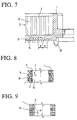
- each terminal 3 is composed of an elongated contact portion 13, a solder tail portion 14 connected to one end of the contact portion 13 and extending outwardly therefrom.
- a mold engagement portion 15 is connected to the other end of the contact portion 13 and is set within the connector housing sidewalls 19, 20.
- the contact portion 13 is exposed along the central space 9 of the housing 1, and serves to provide contact with an opposing terminal of the plug housing.
- the solder tail portion 14 extends out of the bottom 21 of the housing 1.
- the engagement portion 15 is situated in a recess 30 made in the top of the housing 1. As shown, a portion of each terminal 3 is embedded in the housing 1.
- terminals 3 Prior to the mounting of terminals 3 to the housing 1, these terminals 3 exist in a form wherein they are connected to a lateral carrier strip 4 via joint parts 5 (FIGS. 11 and 12) to define a series arrangement of terminals 2 which have a predetermined pitch P.
- the carrier strip-terminal assembly is formed by stamping and forming such that each terminal is formed so as to have a body portion 6 (synonymous with the contact portion 13 illustrated in FIGS. 5-7) interconnected to the carrier strip 4 by means of a joint portion 5, which when cut along line C, defines the solder tail portion 14 of each terminal 3.
- Each terminal of the arrangement 2 has a tapered free-end 7.
- the free-end 7 has two opposing angled sides or surfaces 8 converging toward the centerline 10 of each terminal.
- the carrier strip 4 is cut along the line C (FIG. 12) and is removed from the arrangement of terminals 2.
- the remaining portion of the joint portion 5 serves as the solder tail portion, which is soldered to a selected conductor on a printed circuit board (not shown).
- the housing 1 has positioning pegs 22 on its bottom 21 (FIGS. 4 and 7) so that the electrical connector 1 may be fixed to a printed circuit board with the positioning pegs 22 fitted in the positioning holes of the printed circuit board.
- the tapered free-end 7 (FIGS. 11-13) of each terminal 3 serves as the mold engagement portion.
- the tapered free-end 7 of the terminal 3 has opposing slanted edges or surfaces 8 inclined symmetrically with respect to the centerline 10 between the opposite parallel sides 11 and 12 of the rectangular terminal body.
- This symmetrical shape of the tapered free-end is advantageous to help in laterally aligning terminals 3 at the correct terminal spacing or pitch P.
- the arrangement of terminals 3 at exact intervals is attained by using appropriate jig means having notches 18 arranged at regular intervals corresponding to the intervals P at which all terminals 3 are to be arranged when mounted in the housing 1.
- jig means is used to keep all terminals 3 arranged at exact intervals P by interdigitally nesting the tapered free-ends 7 of the terminals 3 with the counter notches of the jig means.
- the terminal tails 14 are positioned by virtue of their connection to the carrier strip but the mold engagement portions 15 are not positioned because they are free ends.
- irregular arrangement or spacing of terminals can be substantially reduced in a forcible manner by the jig means until the terminals 3 are put in correct position.
- Such jig means is preferably provided in the form of a series of notches in either one of the mold parts 16 and 17. (FIG. 13)
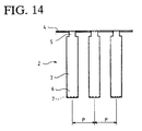
- the array of terminals 3 is placed between the two mold parts 16 and 17 with the tapered free-end 7 of each terminal 3 fitted in the corresponding notch in the mold part prior to injection molding, thereby assuring arrangement of all terminals 3 at exact intervals P, which is effective in maintaining very small pitches, such as 0.625mm or the like.
- FIG. 13 two mold parts 16 and 17 are used for molding insulative connector housings 1 as is known in the art.
- An array 2 of terminals 3 (FIG. 12) having been previously stamped and formed as described above is placed between the mold parts 16 and 17, and an insulative material, such as plastic, is injection-molded therearound. Thereafter, the mold parts 16 and 17 are removed to leave an electrical connector having the arrangement 2 of terminals 3 arranged at regular intervals P and embedded in the insulation housing 1.
- one of the inside and outside mold parts 16 and 17 (outside mold part 16 in FIG. 13) has a series of notches 18 spaced at regular intervals corresponding to the interval P at which the arrangement 2 of terminals 3 are to be set.
- the array 2 of terminals 3 is connected to its associated carrier strip 4, and each terminal 3 has a tapered free-end 7 corresponding in shape and size to the notch 18 made in the mold block 16.
- the terminal arrangement 2 is placed between the mold block 16 and 17 with the tapered free-end 7 of each terminal 3 fitted in the corresponding notch 18 in the mold part 16 prior to injection molding.
- the notchless mold block 17 (shown on the inside of FIG. 13) pushes all of the terminals 3 against the notched mold block 16, thereby forcibly reducing any deviations N which may occur by providing a force M as indicated by arrow M in FIG. 13, to thus arrange all of the terminals 3 at their intended pitch intervals P as seen in FIG. 14.
- the notched mold 16 may have a series of projections (shown) formed thereon to properly position and support the terminals 3 prior to and during molding. These mold projections form a series of holes 23. These holes 23 can be used for testing the terminals 3 if desired.
- FIGS. 8 and 10 illustrate the shape of the insulative housing 1 made by using an outer mold 16 having a series of notches 18 and an inner mold 17 having no notches. The resultant notches 24 are formed in the connector housing 1 as a result of the configuration of the mold block 16 and have no adverse effect on the function of the electric connector. Since the notches 18 of the mold engage the slanted edges 8 of terminal engagement portions 15, substantially no plastic is molded onto these edges. There is, however, plastic above and below the engagement portions 15.
- the electrical connector is described as a receptacle, but it may be a plug-style electrical connector.
- the tapered free-end of the terminal is described above as converging toward the center line 10, thus defining two opposing slanted edges extending from the opposing parallel sides 11 and 12 of the terminal rectangular body.
- the tapered free-ends of the terminals may also have a single slanted edge inclining from one of its opposing parallel sides 11 and 12 of the terminal rectangular body and traversing the centerline 10 and ending at the other parallel side of the terminal rectangular body.
- the single inclined edge can be formed more easily than the double angled edge in the tapered end of the terminal.
- other tapered surfaces such as arcuate, stepped or other shapes that would accurately guide and position the tapered ends into the recesses in the mold could be used.
- terminals according to the present invention have tapered free-ends formed so as to be complimentary in shape to counter notches made in either of the inner and outer molds, thereby permitting corrective adjustment of terminals thus to arrange them at exact intervals in injection molding.
Abstract
Description
- The present invention relates to terminals used in electrical connectors and a method of making electrical connectors, and more particularly to an improved terminal assembly of reduced pitch which assures reliable arrangement during mounting in an associated connector housing, as well as a method of making electrical connectors using such terminals.
- As is well known, electrical connectors are used to connect different electrical components to each other, and wires to printed circuit boards in various electrical apparatus. Such connectors are of multi-pole or terminal structure and use a plurality of terminals laterally arranged at regular intervals and fixed to the housing of the connector. Each terminal typically has a solder tail portion extending from the base of the housing for soldering to an associated wire or electrical trace or contact pad.
- In making such connectors, a plurality of terminals may be either press-fitted in corresponding holes of a connector housing, or may be embedded in the housing during injection molding of the housing. Specifically, a plurality of terminals may be integrally connected in series to an associated lateral carrier strip, and the series is either press-fit into the connector housing or embedded as a whole in the housing by injection molding an insulative material, such as a plastic, therearound. Finally, the lateral carrier strip is cut and separated from the terminals thus press-fitted or embedded in the housing.
- In the injection molding of connector housings, inner and outer molds are used to define a mold cavity and a series terminal-arrangement is inserted therebetween, so that an insulative housing may be molded with the series terminal-arrangement embedded therein. Then, the inner and outer molds are removed and the carrier strip is cut and removed to provide an electric connector.
- Undesired irregular arrangement of terminals, however, may occur in press-fitting terminals into the holes of a housing or when inserting them into a mold cavity where terminals and the inner and outer molds are potentially misaligned relative to each other. The terminals are very thin and small, and therefore, they are prone to being misaligned or bent. As the pitch of the terminals (i.e., the spacing between adjacent terminals) decreases, the potential for misalignment during assembly of the terminals into a connector housing increases.
- In an attempt to reduce such problems, some proposals have been made for the manner of press-fitting or for special jigs for setting terminals in molds and special designed molds. Such proposals are satisfactory to some extent in improving precision of products, but they require extra steps and complicated or time-consuming work. Accordingly the manufacturing cost increases, and the manufacturing efficiency decreases.
- It is therefore an object of the invention to provide electrical connectors in which the terminals are substantially free of the disadvantages described above, assuring the exact positioning of terminals in their associated connector housings and attaining substantial improvement of production thereof.
- Another object of the invention is to provide a method of making electrical connectors using terminals having a very small pitch.
- To attain these objects, a group of terminals are laterally arranged at regular intervals and connected to a lateral carrier strip via joint portions and contained within an insulative housing. Each terminal has a tapered end at the side opposite to the side on which the terminal is connected to the lateral carrier strip.
This tapered end may converge toward the centerline of the terminal, thus defining two opposing angled, or slanted, surfaces extending from the opposite parallel sides of the terminal rectangular body. - An electrical connector comprising an insulative housing and a group of terminals arranged at regular intervals and mounted to the housing, is therefore improved according to the present invention in that each terminal has a contact portion, a first end at one end thereof and a mold engagement portion at the other end thereof, the engagement portion having a tapered end.
- In mounting a plurality of terminals in a connector housing, the arranging of such terminals at reliable and exact intervals can be attained by using appropriate jig means in the form of specially configured mold components having notches arranged at regular intervals corresponding to the desired intervals between the terminals and at which the terminals are to be arranged when fixed in the connector housing. The jig means is used to keep all terminals arranged at exact intervals by interdigitally nesting the tapered ends of the terminals with the notches of the jig means. Thus, irregular arrangement of terminals may be substantially reduced once these terminals are put in the jig means.
- Such jig means may be provided in the form of a series of notches in one of the connector housing mold components. The arrangement of terminals are secured between the inside and outside mold components or blocks with the tapered end of each terminal fitted in the corresponding notch in the appropriate mold part prior to injection molding, thereby assuring arrangement of all terminals at exact intervals.
- The present invention also leads itself to a method of making electrical connector, which includes the steps of: providing interengaging mold components that form a cavity for molding insulative connector housings; placing a group of terminals into the mold cavity defined by the mold components; injection-molding an insulative material into the mold cavity and about a portion of the group of terminals, then removing the mold components to expose an electrical connector having the group of terminals arranged at regular intervals and embedded in the insulative connector housing. Such a method is improved according to the present invention in that one of the mold components is provided with a series of notches formed therein at regular intervals corresponding to those at which the group of terminals are to be arranged; the group of terminals are integrally connected to an associated carrier strip, each terminal having a tapered end complementary in shape to the notch made in the appropriate mold component; and the group of terminals are put between the interfitting mold components with the tapered free-end of each terminal fitted in the mold component notch prior to injection molding, thereby assuring arrangement of all terminals at exact intervals.
- Other objects and advantages of the present invention will be understood from the following description of a preferred embodiment of the present invention.
- In the course of the following detailed description, reference will be made to the attached drawings wherein like reference numerals identify like parts and wherein:
- FIG. 1 is an elevational view of an electrical connector constructed in accordance with the principles of the present invention;
- FIG. 2 is a top plan view of the electrical connector of FIG. 1;
- FIG. 3 is a bottom plan view of the electrical connector of FIG. 1;
- FIG. 4 is an end view of the electrical connector of FIG. 1 taken along lines 4-4 thereof;
- FIG. 5 is a cross sectional view of the electrical connector of FIG. 2 taken along the line F-F thereof;
- FIG. 6 is a cross sectional view of the electrical connector of FIG. 2 taken along the line E-E thereof;
- FIG. 7 is a longitudinal section of a portion of electrical connector of FIG. 2 taken along the line G-G thereof;
- FIG. 8 is a longitudinal section of a portion of electrical connector of FIG 6 taken along the line J-J thereof;
- FIG. 9 is a longitudinal section of a portion of electrical connector of FIG. 6 taken along the line K-K thereof;
- FIG. 10 is an enlarged perspective view of a portion of electrical connector of FIG. 1;
- FIG. 11 is an enlarged perspective view of a portion of the group of terminals integrally connected to their lateral carrier strip;
- FIG. 12 is a perspective view of a portion of the group of terminals connected to a carrier strip, showing how they are placed into a mold cavity between inner and outer mold blocks;
- FIG. 13 is a longitudinal section of the terminals of FIG. 12 taken along the line X-X thereof after positioned in place within the mold blocks, and;
- FIG. 14 is a front view of terminals as seen in the direction indicated by arrow M in Fig. 13.
- Referring to FIGS. 1-6, an electrical connector is shown as a receptacle housing with a central
elongated space 9 and a plurality ofterminals 3 arranged at regular intervals P in itsinsulative housing 1. Specifically, all of theterminals 3 are arranged laterally at regular intervals P in thecentral space 9 defined byopposite side walls central space 9 is adapted to receive a mating electrical connector, that is, a plug housing (not shown) for establishing a required electrical connection between the two connector components. - As the trend for reduction in size of consumer electronics grows, the need for connectors of reduced size likewise increases. One way to reduce the overall size of electrical connectors is to reduce the pitch of the connectors, that is, the spacing between adjoining connector terminals. By reducing the pitch, a connector of a given size may accommodate more circuits. The reduction in pitch down to 0.625 mm and the like typically necessitates a reduction in the size of the terminals. As the size of the terminals decrease, the fragility of the terminals increases and the potential for misalignment occurring after the stamping of the terminals increases. Although in a stamping and forming process, the terminal tail portions which extend out from a carrier strip are secured in a predetermined position which can maintain the pitch at that position, the free ends, in this case the engagement portions, are not. The present invention is directed to a solution for this problem.
- Referring now to FIGS. 5-7, it can be seen that each
terminal 3 is composed of anelongated contact portion 13, asolder tail portion 14 connected to one end of thecontact portion 13 and extending outwardly therefrom. Amold engagement portion 15 is connected to the other end of thecontact portion 13 and is set within theconnector housing sidewalls contact portion 13 is exposed along thecentral space 9 of thehousing 1, and serves to provide contact with an opposing terminal of the plug housing. Thesolder tail portion 14 extends out of thebottom 21 of thehousing 1. Finally, theengagement portion 15 is situated in a recess 30 made in the top of thehousing 1. As shown, a portion of eachterminal 3 is embedded in thehousing 1. - Prior to the mounting of
terminals 3 to thehousing 1, theseterminals 3 exist in a form wherein they are connected to alateral carrier strip 4 via joint parts 5 (FIGS. 11 and 12) to define a series arrangement ofterminals 2 which have a predetermined pitch P. The carrier strip-terminal assembly is formed by stamping and forming such that each terminal is formed so as to have a body portion 6 (synonymous with thecontact portion 13 illustrated in FIGS. 5-7) interconnected to thecarrier strip 4 by means of ajoint portion 5, which when cut along line C, defines thesolder tail portion 14 of eachterminal 3. Each terminal of thearrangement 2 has a tapered free-end 7. - The free-
end 7 has two opposing angled sides orsurfaces 8 converging toward thecenterline 10 of each terminal. After completing the mounting ofterminals 3 to thehousing 1, thecarrier strip 4 is cut along the line C (FIG. 12) and is removed from the arrangement ofterminals 2. The remaining portion of thejoint portion 5 serves as the solder tail portion, which is soldered to a selected conductor on a printed circuit board (not shown). - The
housing 1 has positioning pegs 22 on its bottom 21 (FIGS. 4 and 7) so that theelectrical connector 1 may be fixed to a printed circuit board with the positioning pegs 22 fitted in the positioning holes of the printed circuit board. The tapered free-end 7 (FIGS. 11-13) of each terminal 3 serves as the mold engagement portion. - As described earlier, the tapered free-
end 7 of theterminal 3 has opposing slanted edges or surfaces 8 inclined symmetrically with respect to thecenterline 10 between the oppositeparallel sides terminals 3 at the correct terminal spacing or pitch P. - In mounting
terminals 3 in theconnector housing 1, the arrangement ofterminals 3 at exact intervals is attained by using appropriate jig means havingnotches 18 arranged at regular intervals corresponding to the intervals P at which allterminals 3 are to be arranged when mounted in thehousing 1. Specifically such jig means is used to keep allterminals 3 arranged at exact intervals P by interdigitally nesting the tapered free-ends 7 of theterminals 3 with the counter notches of the jig means. Without the use of such jig means, theterminal tails 14 are positioned by virtue of their connection to the carrier strip but themold engagement portions 15 are not positioned because they are free ends. Thus, irregular arrangement or spacing of terminals can be substantially reduced in a forcible manner by the jig means until theterminals 3 are put in correct position. Such jig means is preferably provided in the form of a series of notches in either one of themold parts terminals 3 is placed between the twomold parts end 7 of each terminal 3 fitted in the corresponding notch in the mold part prior to injection molding, thereby assuring arrangement of allterminals 3 at exact intervals P, which is effective in maintaining very small pitches, such as 0.625mm or the like. - The method of making electrical connectors having small pitch terminals according to the present invention will now be described. As shown in FIG. 13, two
mold parts insulative connector housings 1 as is known in the art. Anarray 2 of terminals 3 (FIG. 12) having been previously stamped and formed as described above is placed between themold parts mold parts arrangement 2 ofterminals 3 arranged at regular intervals P and embedded in theinsulation housing 1. As described above, one of the inside and outsidemold parts 16 and 17 (outsidemold part 16 in FIG. 13) has a series ofnotches 18 spaced at regular intervals corresponding to the interval P at which thearrangement 2 ofterminals 3 are to be set. - The
array 2 ofterminals 3 is connected to its associatedcarrier strip 4, and each terminal 3 has a tapered free-end 7 corresponding in shape and size to thenotch 18 made in themold block 16. Theterminal arrangement 2 is placed between themold block end 7 of each terminal 3 fitted in the correspondingnotch 18 in themold part 16 prior to injection molding. Simultaneously, the notchless mold block 17 (shown on the inside of FIG. 13) pushes all of theterminals 3 against the notchedmold block 16, thereby forcibly reducing any deviations N which may occur by providing a force M as indicated by arrow M in FIG. 13, to thus arrange all of theterminals 3 at their intended pitch intervals P as seen in FIG. 14. - Whereas the
terminal tail portions 14 are positioned by means of their connection to thecarrier strip 4, the mold engagement portions 15 (by way of their free ends 7) are now positioned with the notchedmold block 16 and held thereagainst bymold block 17. This corrective arrangement can be performed at an increased efficiency, and accordingly, highly precise electrical connectors can be produced more efficiently. - The notched
mold 16 may have a series of projections (shown) formed thereon to properly position and support theterminals 3 prior to and during molding. These mold projections form a series ofholes 23. Theseholes 23 can be used for testing theterminals 3 if desired. FIGS. 8 and 10 illustrate the shape of theinsulative housing 1 made by using anouter mold 16 having a series ofnotches 18 and aninner mold 17 having no notches. Theresultant notches 24 are formed in theconnector housing 1 as a result of the configuration of themold block 16 and have no adverse effect on the function of the electric connector. Since thenotches 18 of the mold engage the slantededges 8 ofterminal engagement portions 15, substantially no plastic is molded onto these edges. There is, however, plastic above and below theengagement portions 15. - In this particular embodiment, the electrical connector is described as a receptacle, but it may be a plug-style electrical connector. The tapered free-end of the terminal is described above as converging toward the
center line 10, thus defining two opposing slanted edges extending from the opposingparallel sides parallel sides centerline 10 and ending at the other parallel side of the terminal rectangular body. The single inclined edge can be formed more easily than the double angled edge in the tapered end of the terminal. In addition, other tapered surfaces such as arcuate, stepped or other shapes that would accurately guide and position the tapered ends into the recesses in the mold could be used. - As may be understood from the above, terminals according to the present invention have tapered free-ends formed so as to be complimentary in shape to counter notches made in either of the inner and outer molds, thereby permitting corrective adjustment of terminals thus to arrange them at exact intervals in injection molding.
Claims (18)
- An electrical connector (1) comprising:
an insulative housing having a pair of spaced apart, generally parallel sidewalls (19, 20);
a plurality of terminals (3) mounted in said housing generally along the length of said housing sidewalls, said terminals being generally parallel and spaced apart a predetermined distance; and
each terminal including a first end (14) for interconnection to an electrical component, a second opposite end (15) positioned within said housing, and a terminal body portion (6) between said first and second ends, each said second end having a tapered portion (7) adapted for engagement with a correspondingly shaped recess (18) in a mold component (16) to maintain said terminal second ends in a predetermined array said predetermined distance (P) apart in order to maintain said terminal body portions in a generally parallel array and spaced apart said predetermined distance prior to overmolding said housing about said terminals. - The electrical connector as defined in claim 1, wherein each of said terminal body portions has two generally parallel sides (11, 12) which define a width of each of said terminals, and each of said second ends has at least one tapered end edge (8) extending from one of said body portion sides towards a centerline (10) of said terminal.
- The electrical connector as defined in claim 2, wherein substantially no plastic is molded onto said tapered end edge of said second end upon overmolding said housing about said terminals.
- The electrical connector as defined in claim 2, wherein each of said terminal second ends includes two tapered end edges extending from said generally parallel sides of said body portions toward said terminal centerline.
- The electrical connector as defined in claim 4, wherein said two tapered end edges converge and intersect with each other generally at said centerline to define said tapered second end of said terminals.
- The electrical connector as defined in claim 5 wherein said first end is a solder tail for solder interconnection to circuitry of an electronic circuit.
- The electrical connector as defined in claim 1, wherein each of said terminal second ends has two generally parallel sides and at least one tapered end edge extending from one of said second end sides towards a centerline of said second end.
- The electrical connector as defined in claim 7, wherein substantially no plastic is molded onto said tapered end edge of said second end upon overmolding said housing about said terminals.
- The electrical connector as defined in claim 8, wherein each of said terminal second ends includes two tapered end edges extending from said generally parallel sides of said second ends toward said centerline.
- The electrical connector as defined in claim 9, wherein said two tapered end edges converge and intersect with each other generally at said centerline to define said tapered portion of said second end of said terminals.
- The electrical connector as defined in claim 1, wherein said body portion of each terminal is generally rectangular and said first and second ends are generally parallel.
- The electrical connector as defined in claim 11, wherein said first and second ends extend away from said terminal body portions.
- The electrical connector as defined in claim 1, wherein said housing includes a series of projections extending from said housing sidewalls and generally conforming to the shape of said tapered portion of said second end of said terminals.
- The electrical connector as defined in claim 13, wherein substantially no plastic is molded onto said tapered end edge of said second end upon overmolding said housing about said terminals.
- A method of manufacturing an electrical connector having an insulative housing (1) molded about a plurality of terminals (3), said insulative housing having a pair of spaced apart, generally parallel sidewalls (19, 20), said plurality of terminals being mounted in said housing generally along the length of said housing sidewalls, said terminals being generally parallel and spaced apart a predetermined distance, the method comprising the steps of:
providing interengaging mold components (16, 17) that cooperate to define a mold cavity corresponding to the configuration of said connector housing, at least one of said mold components having a series of engagement recesses (18) in a surface thereof, said recesses being spaced apart said predetermined distance (P);
providing a carrier strip assembly (2) having an elongated carrier strip (4) with a plurality of stamped and formed terminals (3) extending generally transversely from said strip spaced apart said predetermined distance, each terminal including a first end (14) for interconnection to an electrical component, a second opposite, cantilevered end (15) for positioning within said housing, and a terminal body portion (6) between said first and second ends, each said terminal being connected to said carrier strip generally adjacent said first end, said carrier strip maintaining said terminals in an array spaced apart by said predetermined distance, each said second end having a tapered portion (8) adapted for engagement with one of said engagement recesses in said at least one mold component, said tapered portion and said engagement recess being correpondingly shaped to maintain said terminal second ends in a predetermined array said predetermined distance apart within said mold cavity in order to maintain said terminal body portions in a generally parallel array and spaced apart said predetermined distance prior to overmolding said housing about said terminals,
inserting said tapered portion of said terminal second ends into said mold component recesses in order to align said second ends in an array said predetermined distance apart;
securing said carrier strip assembly substantially within said mold cavity; and
injecting an insulative molding material into said mold cavity defined by said mold components to form said connector housing about said terminals. - The method of claim 15, further including the step of removing said terminals from said carrier strip adjacent said first ends to define free solder tail portions extending away from said connector housing.
- The method of claim 15, further including the step of holding said terminals proximate their body portion during said injection molding in order to define a series of openings (23) in said connector housings in which a portion of said terminals are exposed.
- The method of claim 15, wherein said securing step includes clamping said carrier strip assembly between some of said mold components.
Applications Claiming Priority (3)
| Application Number | Priority Date | Filing Date | Title |
|---|---|---|---|
| JP6188973A JP2932152B2 (en) | 1994-07-19 | 1994-07-19 | Terminal for electrical connector and method of forming electrical connector |
| JP188973/94 | 1994-07-19 | ||
| JP18897394 | 1994-07-19 |
Publications (3)
| Publication Number | Publication Date |
|---|---|
| EP0693802A2 true EP0693802A2 (en) | 1996-01-24 |
| EP0693802A3 EP0693802A3 (en) | 1996-03-06 |
| EP0693802B1 EP0693802B1 (en) | 2000-03-08 |
Family
ID=16233172
Family Applications (1)
| Application Number | Title | Priority Date | Filing Date |
|---|---|---|---|
| EP95110652A Expired - Lifetime EP0693802B1 (en) | 1994-07-19 | 1995-07-08 | Electrical connector terminal and method of making electrical connector with same |
Country Status (6)
| Country | Link |
|---|---|
| US (1) | US5779505A (en) |
| EP (1) | EP0693802B1 (en) |
| JP (1) | JP2932152B2 (en) |
| KR (1) | KR100192624B1 (en) |
| DE (1) | DE69515388T2 (en) |
| TW (2) | TW425007U (en) |
Cited By (8)
| Publication number | Priority date | Publication date | Assignee | Title |
|---|---|---|---|---|
| EP0762560A2 (en) * | 1995-09-07 | 1997-03-12 | Molex Incorporated | Electrical connector with embedded terminals |
| EP0795929A2 (en) * | 1996-03-14 | 1997-09-17 | Molex Incorporated | Electric connector assembly with improved retention characteristics |
| EP0817324A2 (en) * | 1996-06-28 | 1998-01-07 | Berg Electronics Manufacturing B.V. | Electrical connector for use in miniaturized high density and high pin count applications and method of manufacture |
| EP0849844A2 (en) * | 1996-12-20 | 1998-06-24 | Molex Incorporated | Insert molded electrical connector and method of producing same |
| EP0886344A2 (en) * | 1997-06-20 | 1998-12-23 | Molex Incorporated | Terminal retention system |
| EP0930670A2 (en) * | 1998-01-16 | 1999-07-21 | Japan Solderless Terminal Mfg Co Ltd | Electric connector and a method of making same |
| EP1414111A1 (en) * | 2002-10-23 | 2004-04-28 | J.S.T. Mfg. Co., Ltd. | Connector and method for producing thereof |
| CN110137727A (en) * | 2018-02-09 | 2019-08-16 | 富士康(昆山)电脑接插件有限公司 | Electric connector and its manufacturing method |
Families Citing this family (20)
| Publication number | Priority date | Publication date | Assignee | Title |
|---|---|---|---|---|
| US6004160A (en) * | 1997-03-25 | 1999-12-21 | The Whitaker Corporation | Electrical connector with insert molded housing |
| JP3356394B2 (en) * | 1997-10-23 | 2002-12-16 | タイコエレクトロニクスアンプ株式会社 | Electrical contacts |
| TW445679B (en) * | 1998-12-31 | 2001-07-11 | Hon Hai Prec Ind Co Ltd | Method for manufacturing modular terminals of electrical connector |
| US6187246B1 (en) | 1998-12-31 | 2001-02-13 | Berg Technology, Inc. | Method of manufacturing an extended height insulative housing for an electrical connector |
| TW445676B (en) * | 1999-06-24 | 2001-07-11 | Hon Hai Prec Ind Co Ltd | Electrical connector structure |
| CN1133246C (en) * | 1999-07-20 | 2003-12-31 | 富士康(昆山)电脑接插件有限公司 | Structure of electric connector |
| CN1095603C (en) * | 1999-07-20 | 2002-12-04 | 富士康(昆山)电脑接插件有限公司 | Structure of electric connector |
| CN1095604C (en) * | 1999-07-20 | 2002-12-04 | 富士康(昆山)电脑接插件有限公司 | Structure of electric connector |
| US6176744B1 (en) * | 1999-10-01 | 2001-01-23 | Motorola, Inc. | Plated plastic connection system and method of making |
| US6200171B1 (en) | 1999-11-30 | 2001-03-13 | Berg Technology, Inc. | Electrical connector with over-molded housing member and method of over-molding |
| CA2501144C (en) | 2002-10-23 | 2015-10-06 | University Of Utah Research Foundation | Amplicon melting analysis with saturation dyes |
| JP3961937B2 (en) * | 2002-11-26 | 2007-08-22 | 日本圧着端子製造株式会社 | Board electrical connector |
| TWM249315U (en) * | 2003-08-06 | 2004-11-01 | Hon Hai Prec Ind Co Ltd | Electrical connector |
| DE10339594A1 (en) * | 2003-08-26 | 2005-03-24 | Patent-Treuhand-Gesellschaft für elektrische Glühlampen mbH | Lamp base for a high-pressure discharge lamp and high-pressure discharge lamp |
| US6966800B2 (en) * | 2004-03-22 | 2005-11-22 | Fci Americas Technology, Inc. | Overmolded electrical connector |
| US9657347B2 (en) | 2004-04-20 | 2017-05-23 | University of Utah Research Foundation and BioFire Defense, LLC | Nucleic acid melting analysis with saturation dyes |
| KR101014196B1 (en) * | 2010-04-26 | 2011-02-14 | 주식회사 폴리사이언텍 | Tube type film for package and manufacturing method thereof |
| CN102157879B (en) * | 2010-12-31 | 2013-02-27 | 番禺得意精密电子工业有限公司 | Method for manufacturing electrical connector |
| CN104338886B (en) * | 2013-08-05 | 2017-02-08 | 机械科学研究总院青岛分院 | Pop rivet automatically stapling device |
| JP6960748B2 (en) * | 2017-03-07 | 2021-11-05 | ヒロセ電機株式会社 | Electrical connector and electrical connector assembly |
Family Cites Families (11)
| Publication number | Priority date | Publication date | Assignee | Title |
|---|---|---|---|---|
| US3348191A (en) * | 1964-03-05 | 1967-10-17 | Amp Inc | Electrical connector elements |
| US4106841A (en) * | 1977-03-11 | 1978-08-15 | Bunker Ramo Corporation | Electrical connector for printed circuit boards |
| JPS5882786U (en) * | 1981-11-30 | 1983-06-04 | ソニー株式会社 | multi connector |
| JPS5951115A (en) * | 1982-09-17 | 1984-03-24 | Nippon Soken Inc | Variable valve controller for internal-combustion engine |
| US4863402A (en) * | 1986-10-17 | 1989-09-05 | Ohio Associated Enterprises, Inc. | Method and apparatus for making electrical connecting device |
| US4865562A (en) * | 1988-02-01 | 1989-09-12 | Minnesota Mining And Manufacturing Company | Overmolded electrical contact for the manufacture of connectors |
| JP2786667B2 (en) * | 1989-04-14 | 1998-08-13 | 和泉電気株式会社 | Manufacturing type of electric parts row |
| US5350322A (en) * | 1990-02-22 | 1994-09-27 | Yazaki Corporation | Bulb socket terminal |
| JPH04181676A (en) * | 1990-11-15 | 1992-06-29 | Hirose Electric Co Ltd | Electric connector and manufacture thereof |
| JP3078616B2 (en) * | 1991-08-30 | 2000-08-21 | ケル株式会社 | Plug connector and manufacturing method thereof |
| JP2541653Y2 (en) * | 1993-05-21 | 1997-07-16 | 日本航空電子工業株式会社 | connector |
-
1994
- 1994-07-19 JP JP6188973A patent/JP2932152B2/en not_active Expired - Lifetime
-
1995
- 1995-06-12 US US08/489,470 patent/US5779505A/en not_active Expired - Lifetime
- 1995-06-20 TW TW088205931U patent/TW425007U/en unknown
- 1995-06-20 TW TW084106310A patent/TW365080B/en not_active IP Right Cessation
- 1995-07-08 DE DE69515388T patent/DE69515388T2/en not_active Expired - Fee Related
- 1995-07-08 EP EP95110652A patent/EP0693802B1/en not_active Expired - Lifetime
- 1995-07-18 KR KR1019950020966A patent/KR100192624B1/en not_active IP Right Cessation
Non-Patent Citations (1)
| Title |
|---|
| None |
Cited By (21)
| Publication number | Priority date | Publication date | Assignee | Title |
|---|---|---|---|---|
| EP0762560A2 (en) * | 1995-09-07 | 1997-03-12 | Molex Incorporated | Electrical connector with embedded terminals |
| EP0762560A3 (en) * | 1995-09-07 | 1998-04-08 | Molex Incorporated | Electrical connector with embedded terminals |
| EP0795929A3 (en) * | 1996-03-14 | 1998-11-25 | Molex Incorporated | Electric connector assembly with improved retention characteristics |
| EP0795929A2 (en) * | 1996-03-14 | 1997-09-17 | Molex Incorporated | Electric connector assembly with improved retention characteristics |
| SG93815A1 (en) * | 1996-06-28 | 2003-01-21 | Connector Systems Tech Nv | Electrical connector for use in miniaturized, high density, and high pin count applications and method of manufacture |
| US6048482A (en) * | 1996-06-28 | 2000-04-11 | Berg Technology, Inc. | Method for manufacturing an electrical connector |
| EP0817324A2 (en) * | 1996-06-28 | 1998-01-07 | Berg Electronics Manufacturing B.V. | Electrical connector for use in miniaturized high density and high pin count applications and method of manufacture |
| EP0817324A3 (en) * | 1996-06-28 | 1999-10-20 | Berg Electronics Manufacturing B.V. | Electrical connector for use in miniaturized high density and high pin count applications and method of manufacture |
| US6065951A (en) * | 1996-06-28 | 2000-05-23 | Berg Technology, Inc. | Mold for use in manufacturing an electrical connector |
| EP0849844A3 (en) * | 1996-12-20 | 1999-07-21 | Molex Incorporated | Insert molded electrical connector and method of producing same |
| EP0849844A2 (en) * | 1996-12-20 | 1998-06-24 | Molex Incorporated | Insert molded electrical connector and method of producing same |
| US6099359A (en) * | 1997-06-20 | 2000-08-08 | Molex Incorporated | Terminal retention system |
| EP0886344A3 (en) * | 1997-06-20 | 1999-11-24 | Molex Incorporated | Terminal retention system |
| EP0886344A2 (en) * | 1997-06-20 | 1998-12-23 | Molex Incorporated | Terminal retention system |
| CN1125516C (en) * | 1997-06-20 | 2003-10-22 | 莫列斯公司 | Terminal retention system |
| EP0930670A2 (en) * | 1998-01-16 | 1999-07-21 | Japan Solderless Terminal Mfg Co Ltd | Electric connector and a method of making same |
| EP0930670A3 (en) * | 1998-01-16 | 2000-10-18 | Japan Solderless Terminal Mfg Co Ltd | Electric connector and a method of making same |
| EP1414111A1 (en) * | 2002-10-23 | 2004-04-28 | J.S.T. Mfg. Co., Ltd. | Connector and method for producing thereof |
| US6988916B2 (en) | 2002-10-23 | 2006-01-24 | J.S.T. Mfg., Co., Ltd. | Connector and method for producing thereof |
| CN100341204C (en) * | 2002-10-23 | 2007-10-03 | 日本压着端子制造株式会社 | Connector and manufacturing method of connector |
| CN110137727A (en) * | 2018-02-09 | 2019-08-16 | 富士康(昆山)电脑接插件有限公司 | Electric connector and its manufacturing method |
Also Published As
| Publication number | Publication date |
|---|---|
| TW365080B (en) | 1999-07-21 |
| TW425007U (en) | 2001-03-01 |
| DE69515388D1 (en) | 2000-04-13 |
| JP2932152B2 (en) | 1999-08-09 |
| KR100192624B1 (en) | 1999-06-15 |
| EP0693802B1 (en) | 2000-03-08 |
| JPH0831486A (en) | 1996-02-02 |
| DE69515388T2 (en) | 2000-11-02 |
| US5779505A (en) | 1998-07-14 |
| EP0693802A3 (en) | 1996-03-06 |
| KR960006149A (en) | 1996-02-23 |
Similar Documents
| Publication | Publication Date | Title |
|---|---|---|
| EP0693802B1 (en) | Electrical connector terminal and method of making electrical connector with same | |
| US5184963A (en) | Electrical connector with contacts on diestamping centers | |
| US6048482A (en) | Method for manufacturing an electrical connector | |
| US4231628A (en) | Electrical connector receptacles | |
| US6155886A (en) | Electrical connector and method for making the same | |
| KR100216612B1 (en) | Electrical connector with embedded terminals | |
| US5848920A (en) | Fabrication of electrical terminals for edge card connectors | |
| US6231355B1 (en) | Matched impedance connector having retention device on a grounding plane | |
| US5810623A (en) | Edge connector for a printed circuit board | |
| EP0651471B1 (en) | Electrical connector having bus bars providing circuit board retention | |
| EP0846350B1 (en) | Method for making surface mountable connectors | |
| EP0567007A2 (en) | Electrical connector for surface mouting | |
| JP3023282U (en) | Electrical connector | |
| JP3360178B2 (en) | Electrical connector having integral support structure | |
| US5542851A (en) | Electrical connector with improved grounding | |
| JPH06176801A (en) | Wire-termination block | |
| KR980012729A (en) | Corner Connector for Printed Circuit Boards | |
| US5611699A (en) | Tape-carrier-type electrical connector and method of manufacturing same | |
| EP0660460A2 (en) | Electrical connector for mounting on a printed circuit board | |
| US6371816B1 (en) | Electric connector and a method of making same | |
| KR101029668B1 (en) | Surface mount header assembly | |
| US5884393A (en) | Mounting jig for electrical connectors | |
| JP2562970Y2 (en) | Surface mount type connector | |
| US6338633B1 (en) | Electrical connector with improved contacts | |
| US5800203A (en) | Terminal retention for an electrical connector |
Legal Events
| Date | Code | Title | Description |
|---|---|---|---|
| PUAI | Public reference made under article 153(3) epc to a published international application that has entered the european phase |
Free format text: ORIGINAL CODE: 0009012 |
|
| PUAL | Search report despatched |
Free format text: ORIGINAL CODE: 0009013 |
|
| AK | Designated contracting states |
Kind code of ref document: A2 Designated state(s): DE FR GB IT |
|
| AK | Designated contracting states |
Kind code of ref document: A3 Designated state(s): DE FR GB IT |
|
| 17P | Request for examination filed |
Effective date: 19960823 |
|
| 17Q | First examination report despatched |
Effective date: 19961010 |
|
| GRAG | Despatch of communication of intention to grant |
Free format text: ORIGINAL CODE: EPIDOS AGRA |
|
| GRAG | Despatch of communication of intention to grant |
Free format text: ORIGINAL CODE: EPIDOS AGRA |
|
| GRAH | Despatch of communication of intention to grant a patent |
Free format text: ORIGINAL CODE: EPIDOS IGRA |
|
| ITF | It: translation for a ep patent filed |
Owner name: DE DOMINICIS & MAYER S.R.L. |
|
| GRAH | Despatch of communication of intention to grant a patent |
Free format text: ORIGINAL CODE: EPIDOS IGRA |
|
| GRAA | (expected) grant |
Free format text: ORIGINAL CODE: 0009210 |
|
| AK | Designated contracting states |
Kind code of ref document: B1 Designated state(s): DE FR GB IT |
|
| RIC1 | Information provided on ipc code assigned before grant |
Free format text: 7H 01R 12/18 A, 7H 01R 43/24 B |
|
| REF | Corresponds to: |
Ref document number: 69515388 Country of ref document: DE Date of ref document: 20000413 |
|
| ET | Fr: translation filed | ||
| PLBE | No opposition filed within time limit |
Free format text: ORIGINAL CODE: 0009261 |
|
| STAA | Information on the status of an ep patent application or granted ep patent |
Free format text: STATUS: NO OPPOSITION FILED WITHIN TIME LIMIT |
|
| 26N | No opposition filed | ||
| PGFP | Annual fee paid to national office [announced via postgrant information from national office to epo] |
Ref country code: GB Payment date: 20010614 Year of fee payment: 7 |
|
| PGFP | Annual fee paid to national office [announced via postgrant information from national office to epo] |
Ref country code: FR Payment date: 20010702 Year of fee payment: 7 |
|
| PGFP | Annual fee paid to national office [announced via postgrant information from national office to epo] |
Ref country code: DE Payment date: 20010731 Year of fee payment: 7 |
|
| REG | Reference to a national code |
Ref country code: GB Ref legal event code: IF02 |
|
| PG25 | Lapsed in a contracting state [announced via postgrant information from national office to epo] |
Ref country code: GB Free format text: LAPSE BECAUSE OF NON-PAYMENT OF DUE FEES Effective date: 20020708 |
|
| PG25 | Lapsed in a contracting state [announced via postgrant information from national office to epo] |
Ref country code: DE Free format text: LAPSE BECAUSE OF NON-PAYMENT OF DUE FEES Effective date: 20030201 |
|
| GBPC | Gb: european patent ceased through non-payment of renewal fee |
Effective date: 20020708 |
|
| PG25 | Lapsed in a contracting state [announced via postgrant information from national office to epo] |
Ref country code: FR Free format text: LAPSE BECAUSE OF NON-PAYMENT OF DUE FEES Effective date: 20030331 |
|
| REG | Reference to a national code |
Ref country code: FR Ref legal event code: ST |
|
| PG25 | Lapsed in a contracting state [announced via postgrant information from national office to epo] |
Ref country code: IT Free format text: LAPSE BECAUSE OF NON-PAYMENT OF DUE FEES Effective date: 20050708 |