EP0703533A1 - Digital signal processing apparatus - Google Patents
Digital signal processing apparatus Download PDFInfo
- Publication number
- EP0703533A1 EP0703533A1 EP95114933A EP95114933A EP0703533A1 EP 0703533 A1 EP0703533 A1 EP 0703533A1 EP 95114933 A EP95114933 A EP 95114933A EP 95114933 A EP95114933 A EP 95114933A EP 0703533 A1 EP0703533 A1 EP 0703533A1
- Authority
- EP
- European Patent Office
- Prior art keywords
- data
- output
- input
- block
- memory
- Prior art date
- Legal status (The legal status is an assumption and is not a legal conclusion. Google has not performed a legal analysis and makes no representation as to the accuracy of the status listed.)
- Granted
Links
Images


Classifications
-
- G—PHYSICS
- G06—COMPUTING; CALCULATING OR COUNTING
- G06F—ELECTRIC DIGITAL DATA PROCESSING
- G06F9/00—Arrangements for program control, e.g. control units
- G06F9/06—Arrangements for program control, e.g. control units using stored programs, i.e. using an internal store of processing equipment to receive or retain programs
- G06F9/46—Multiprogramming arrangements
- G06F9/50—Allocation of resources, e.g. of the central processing unit [CPU]
- G06F9/5005—Allocation of resources, e.g. of the central processing unit [CPU] to service a request
- G06F9/5027—Allocation of resources, e.g. of the central processing unit [CPU] to service a request the resource being a machine, e.g. CPUs, Servers, Terminals
- G06F9/505—Allocation of resources, e.g. of the central processing unit [CPU] to service a request the resource being a machine, e.g. CPUs, Servers, Terminals considering the load
-
- G—PHYSICS
- G06—COMPUTING; CALCULATING OR COUNTING
- G06F—ELECTRIC DIGITAL DATA PROCESSING
- G06F9/00—Arrangements for program control, e.g. control units
- G06F9/06—Arrangements for program control, e.g. control units using stored programs, i.e. using an internal store of processing equipment to receive or retain programs
- G06F9/46—Multiprogramming arrangements
- G06F9/50—Allocation of resources, e.g. of the central processing unit [CPU]
- G06F9/5061—Partitioning or combining of resources
- G06F9/5066—Algorithms for mapping a plurality of inter-dependent sub-tasks onto a plurality of physical CPUs
-
- G—PHYSICS
- G06—COMPUTING; CALCULATING OR COUNTING
- G06T—IMAGE DATA PROCESSING OR GENERATION, IN GENERAL
- G06T7/00—Image analysis
- G06T7/20—Analysis of motion
- G06T7/223—Analysis of motion using block-matching
-
- H—ELECTRICITY
- H04—ELECTRIC COMMUNICATION TECHNIQUE
- H04N—PICTORIAL COMMUNICATION, e.g. TELEVISION
- H04N19/00—Methods or arrangements for coding, decoding, compressing or decompressing digital video signals
- H04N19/42—Methods or arrangements for coding, decoding, compressing or decompressing digital video signals characterised by implementation details or hardware specially adapted for video compression or decompression, e.g. dedicated software implementation
- H04N19/43—Hardware specially adapted for motion estimation or compensation
- H04N19/433—Hardware specially adapted for motion estimation or compensation characterised by techniques for memory access
-
- H—ELECTRICITY
- H04—ELECTRIC COMMUNICATION TECHNIQUE
- H04N—PICTORIAL COMMUNICATION, e.g. TELEVISION
- H04N19/00—Methods or arrangements for coding, decoding, compressing or decompressing digital video signals
- H04N19/50—Methods or arrangements for coding, decoding, compressing or decompressing digital video signals using predictive coding
- H04N19/503—Methods or arrangements for coding, decoding, compressing or decompressing digital video signals using predictive coding involving temporal prediction
- H04N19/51—Motion estimation or motion compensation
-
- H—ELECTRICITY
- H04—ELECTRIC COMMUNICATION TECHNIQUE
- H04N—PICTORIAL COMMUNICATION, e.g. TELEVISION
- H04N19/00—Methods or arrangements for coding, decoding, compressing or decompressing digital video signals
- H04N19/60—Methods or arrangements for coding, decoding, compressing or decompressing digital video signals using transform coding
- H04N19/61—Methods or arrangements for coding, decoding, compressing or decompressing digital video signals using transform coding in combination with predictive coding
-
- G—PHYSICS
- G06—COMPUTING; CALCULATING OR COUNTING
- G06T—IMAGE DATA PROCESSING OR GENERATION, IN GENERAL
- G06T2207/00—Indexing scheme for image analysis or image enhancement
- G06T2207/10—Image acquisition modality
- G06T2207/10016—Video; Image sequence
-
- H—ELECTRICITY
- H04—ELECTRIC COMMUNICATION TECHNIQUE
- H04N—PICTORIAL COMMUNICATION, e.g. TELEVISION
- H04N19/00—Methods or arrangements for coding, decoding, compressing or decompressing digital video signals
- H04N19/30—Methods or arrangements for coding, decoding, compressing or decompressing digital video signals using hierarchical techniques, e.g. scalability
Definitions
- the present invention relates to a digital signal processing apparatus which performs computational processes for digital signals.
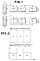
- Fig. 1 shows the multiprocessor system described in article entitled "A Real Time Video Signal Processor Suitable for Motion Picture Coding Applications", IEEE, GLOBCOM '87, p. 453.
- input data 1 is received by a data transfer controller 3, and thereafter data 4 are transferred selectively to digital signal processors 2, i.e. DSP-1 through DSP-N, in block-1.
- digital signal processors 2 i.e. DSP-1 through DSP-N
- resultant data 5 is transferred to block-2 and processed by respective DSPs for the next processing step.
- Fig. 2(a) shows divided memory areas of the DSPs.
- shown here is an example of parallel processing using three DSPs 2, to which process areas A, B and C are assigned evenly.
- the volume of computation needed for the process differs depending on the valid pixel rate even though the number of pixels in the process area is constant.
- the volume of computation or computation time needed is proportional to the valid pixel rate.
- the computation time needed for one block of parallel DSP configuration is determined from the process time of the DSP which works for the area B with the largest volume of process M, and the remaining DSPs which have finished the areas A and C earlier have idle time.
- the conventional digital signal processing apparatus arranged as described above has its overall process time determined from the longest process time among DSPs when the density of information, such as the valid pixel rate, within a frame is uneven and the distribution of information varies with time, resulting in a degraded process efficiency per DSP unit.
- Fig. 3 is a diagram showing, as an example, the arrangement of other digital signal processing apparatus disclosed in an article entitled "Realtime Video Signal Processor Module", in the proceeding of ICASSP '87, pp. 1961 - 1964, April 1987, Dallas, U.S.A.
- 1 an input terminal
- 4 is an input bus for distributing input data on the input terminal
- 28a is a feedback bus for distributing the result of previous process
- 20 are signal processing modules each including an input storage 21, a processing unit 22, an output storage 23 and a timing control unit 24.
- Indicated by 25 are wired-OR circuits through which feedback data on output ports 30 are placed on the feedback bus 28a, 26 are wired-OR circuits through which output data on output ports 29 are delivered to the output terminal 5 over the output bus 5a, 27 are input ports for the input data to the signal processing module 20, and 28 are input ports for the feedback data to the signal processing module 20.
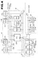
- Fig. 4 is a block diagram showing in more detail one of the signal processing module in Fig. 3.
- 221 is an address generator (AGU A)
- 211 is an input dual memory (MEM A) which receives data on the input port 27 over the input bus 4
- 212 is an input dual memory (MEM B) which receives data on the feedback bus 28a by way of the input port 28
- 222 is an address generator (AGU B)
- 223 is an X-bus
- 224 is a Y-bus
- 225 is a pipeline arithmetic unit (PAU) having its input terminal EX1 connected to the X-bus 223 and another input terminal EX2 connected to the Y-bus 224.
- PAU pipeline arithmetic unit
- Indicated by 226 is a data memory [MEM P(Q)] having its output connected to the X-bus 223, 227 is an address generator [AGU P(Q)] having its output connected to the Y-bus 224 and data memory 226, 228 is a mode register (MDR) having its output connected to the X-bus 223 and Y-bus 224, and 241 is a Z-bus connected to the inputs of the address generators 221, 222 and 227, pipeline arithmetic unit 225 and data memory 226.
- MDR mode register
- Indicated by 242 is a sequencer (SEQ), 243 is an instruction memory (IRAM) connected to the output of the sequencer 242, and 245 is a decoder (DEC) connected to the output of the instruction memory 243, with the output of the decoder 245 being connected to the Z-bus 241 and output bus 231.
- the output bus 231 is connected to the input of the mode register 228 and the Z-bus 241.
- Indicated by 232 is an FIFO memory (MEM C) connected to the output bus 231, 233 is an FIFO (MEM D) connected to the output bus 231, 29 is an output port of the FIFO memory 232, and 30 is an output port of the FIFO memory 233.
- Fig. 5 is a diagram showing, as an example, the algorism of a typical high-efficiency coder for a moving image.
- indicated by 250 is an input terminal for the input video signal
- 251 is an input frame buffer having at least a l-frame capacity and having the simultaneous read-write ability
- 252 is an inter-frame subtracter for evaluating the difference
- 253 is a block identifier
- 254 is a coder
- 255 is a coding parameter produced by the coder 254
- 256 is a variable-length coder
- 257 is a video multiplexer
- 258 is a transmission buffer memory
- 259 is an output terminal for the coded data.
- 260 is a local decoder which receives the coding parameter 255
- 261 is an inter frame adder
- 262 is an in-loop filter
- 263 is a coding frame memory
- 264 is previous coded frame data
- 265 is a motion compensator
- 266 is current frame data fed from the input frame buffer 251 to the motion compensator 265,
- 267 is motion vector data
- 268 is compensated previous frame data fed from the motion compensator 265 to the inter-frame subtracter 252 and inter-frame adder 261
- 269 is a feedback signal
- 270 is a coding controller which provides coding control information for the video multiplexer 257, a feed-forward signal to the input frame buffer 251, a block identification control signal 273 to the block identifier 253, and a coding control signal 274 to the variable-length coder 256.
- This apparatus is intended for moving image processing and is based on the division parallel processing system in which a frame is divided into small frames and a signal processing module 20 is assigned to each of the divided frame areas.
- each signal processing module 20 operates on the autonomous basis by expending one video frame time to fetch a divided frame area assigned to it among the input data transferred frame-wise in raster scanning over the input bus 4 and store the data in the input storage 21.
- each signal processing module 20 operates by expending one video frame time to fetch data of the assigned area of the frame in the feedback data from the input port 28 over the feedback bus 28a and stores the data in the input storage 21.
- the processing unit 22 Upon expiration of one video frame time, the processing unit 22 performs the prescribed signal processing for the input data and feedback data stored in the input storage 21, and stores the result temporarily in the output storage 23.
- the feedback data led out of the output storage 23 through the output port 30 is timed for synchronization with other signal processing modules 20 and, by being merged into all feedback data by the wired-OR circuit 25, placed on the feedback bus 28a.
- the output data led out of the output storage 23 through the output port 29 is timed for synchronization with other signal processing modules 20 and, by being merged into all output data by the wired-OR circuit 26, delivered to the output terminal 5 over the output bus 5a.
- the timing control unit 24 provides all sections of system with the timing of data input/output and process commencement in synchronism with the video frame timing which is the synchronization reference point.
- the input dual memories 211 and 212 is made up of a two-sided memory device in the same structure on both sides and it operates such that while one side is written data, the other side is connected to the X-bus 223 and Y-bus 224 for reading for the coding process by the pipeline arithmetic unit 225.
- the read/write sides of the input dual memories 211 and 212 are switched by the above-mentioned video frame sync signal so that input data of assigned areas on the input ports 27 and 28 are entered frame-wise uninterruptedly.
- the data read out to the X-bus 223 and Y-bus 224 are those stored at data memory addresses indicated to the input dual memories 211 and 212 by the address generators 221 and 222 that are controlled by the signals provided by the decoder 245 by decoding a 80-bit length horizon-type microcodes read out in accordance with the address of the command memory 243 indicated by the sequencer 242.
- the data placed on the X-bus 223 and Y-bus 224 are entered in parallel to the pipeline arithmetic unit 225, which implements a series of signal processing including coding and local decoding and outputs the result to the Z-bus 241.
- the coded output is stored in the FIFO memory 232 and the local decoded output is stored in the FIFO memory 233 by way of the output bus 231.
- the FIFO memories 232 and 233 are buffer memories of FIFO configuration. Feedback data consisting of the output data and local decoded data are read out of the output ports 29 and 30 at the read control timing for the assigned area produced from the video frame signal, and a piece of video frame local decoded data and coded output data in compliance with the scanning order are produced.
- the data memory 226 which is controlled by the output of the address generator 227 is used by a work memory which is necessary for the process of the pipeline arithmetic unit 225 and a table which stores constants.
- the mode register 228 consists of a register file including registers for loading immediate values from the decoder 245.
- This digital signal processing apparatus is principally based on the foregoing area division parallel processing, and is intended such that each signal processing module 20 deals with a divided frame area independently on a realtime basis.
- the digital signal processing apparatus is intended for the achievement of a coder as shown in Fig. 5, only portions excluding the variable-length coder 256, video multiplexer 257, transmission buffer 258 and coding controller 270 can be realized. Namely, it is not suitable for a continuous process in one video frame, and is limited to the inter-frame coding loop process ranging from the input frame buffer 251 to the block identifier 253, coder 254, local decoder 260, coding frame memory 263, and to the motion compensator 265 useful for data completely divisible within a frame.
- the processing program stored in the instruction memory 243 can be a single program.
- M is an integer greater than or equal to 1
- Nc Mc ⁇ Tf/Mp ⁇ Np (clocks/pixel)
- Mc the frequency of machine cycle (Hz)
- Tf the frame period (sec)
- Mp the number of horizontal pixels in the assigned area
- Np the number of vertical pixels in the assigned area.
- the conventional digital signal processing apparatus arranged as described above have the following problems for processing video signals.
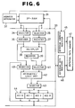
- Fig. 6 is a block diagram of the conventional digital signal processing system disclosed in the proceeding (No. S10-1) of the 1986 annual convention of the communication department of The Institute of Electronics and Communication Engineers of Japan.
- 31 is a dual-port internal data memory (will be termed 2P-RAM) capable of reading and writing two sets of data simultaneously
- 32 is an address generator which calculates the address of read data or write data
- 33 is a data bus used for the internal transfer of data related to computation
- 34 and 35 are selectors which select data in the 2P-RAM 31
- 36 is a register which holds computation data selected by the selector 34
- 35 is a register which holds computation data selected by the selector 35
- 38 is a multiplier
- 39 is a register which holds the output of the multiplier 38
- 40 is a selector which selects the output of the register 36 or accumulators (ACC0 - ACC3) 44
- 41 is a selector which selects the output of the registers 39 or 37
- 42 is an arithmetic
- the accumulators 44 are used to hold the output of the arithmetic/logic unit 42 for cumulative computations.
- the external data register 46 is to hold data from an external data memory 47. Indicated by 45 is an external address register which holds address data provided by the address generator 32 and transfers it to the external data memory 47.
- This signal processing system based on a digital signal processor performs command fetching and decoding for the preset microprogram, data reading, computation, and computation result writing, in a parallel pipeline processing mode.
- the following describes the operation of 3-input-1-output computation.
- the arithmetic/logic unit, multiplier, address generator, data memories and selectors are controlled in the microcommand mode.
- Arithmetic operations for two inputs including addition, subtraction, maximum evaluation, minimum evaluation, etc. are expressed generically by a ⁇ b, and a multiplication operation for two inputs is expressed generically by a x b, where a and b are independent data.
- Fig. 7 shows the sequence of process for implementing the 3-input operation of the form of expression (1) by the digital signal processing system, for example, shown in Fig. 6.
- the data address generator 32 sets up the starting addresses for two data sets A and B , and selects the simple incremental mode Then the two data sets A and B are loaded through the selectors 34 and 35 into the registers 36 and 37.
- the selectors 40 and 41 select the registers 36 and 37, respectively, so that the arithmetic/logic unit 42 implements the arithmetic operation ai ⁇ bi.
- the selector 43 selects the arithmetic/logic unit 42 to hold the operation result temporarily in one of accumulators (ACC0 - ACC3) 44, and the resultant data is sent over the data bus 33 and through the external register 46 and stored in the external memory 47, which addressing mode is the simple incremental mode because of it being linked to one of addresses for the 2P-RAM 31 in the address generator 32.
- step ST3 the data address generator 32 sets up the starting addresses of the data set C and data set ai ⁇ bi, and ci data is read out of the 2P-RAM 31 to the register 36.
- the selector 35 selects the data bus to load the data of ai ⁇ bi in the external memory 47 into the register 37.
- step ST4 needs to expend two cycles of useless command reading for the external memory in advance.
- the two sets of data are rendered multiplication by the multiplier 38 in step ST5, and the result is stored in the register 39.
- the resultant data is passed through the arithmetic/logic unit 42 and, after being held temporarily in one of the accumulators (ACC0 - ACC3) 44, transferred over the data bus 33 to the 2P-RAM 31.
- Table 1 is for the operation of ai ⁇ bi and the transfer of the result to the external memory 47
- Table 2 is for the reading the resultant ai ⁇ bi from the external memory 47, the operation of (ai ⁇ bi) ⁇ ci, and the transfer of the result to the 2P-RAM.
- symbol "x" represents an indefinite value.
- the conventional digital signal processing system is formed as described above, and therefore for a 3-input-1-output operation of three independent data sets, it performs two times of 2-input-1-output operation.
- the process time is further extended for address control, memory transfer and other processes.
- Fig. 8 is a diagram showing in brief the image coding transmitter which implements the conventional motion compensatory operation method disclosed in an article entitled "Dynamic Multistage Vector Quantization for Images", journal of The Institute of Electronics and Communication Engineers of Japan, Vol. J68-B, No. 1, pp. 68 - 76, Jan. 1985.
- an input signal of image data formed of a plurality of consecutive frames on the time axis 52 is a motion compensator which produces a prediction signal on the basis of the resemblance computation of correlation between the current frame represented by the input signal 1 and the previous frame represented by a previous frame signal 53 which is the previous reduced signal 1
- 54 is motion vector information provided by the motion compensator 52 indicative of the position of a prediction signal block
- 55 is a prediction signal produced by the motion compensator 52
- 56 is a coder which codes the difference between the input signal 1 and prediction signal 56
- 57 is a decoder which decodes the signal coded by the coder 56
- 58 is a frame memory which stores data reproduced through the summation of the signal from the decoder 57 and the signal from the motion compensator 52.
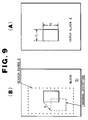
- the motion compensation process is to calculate for the input signal 1 the amount of distortion between a 11-by-12 block located in a specific position in the current frame shown in Fig. 9(A) and M pieces of blocks in the search range S in the previous frame shown in Fig. 9(B) to evaluate the position of the block y providing a minimal distortion relative to the position of the input block, i.e., motion vector V, and to recognize the signal of the minimal distortion block as a prediction signal.
- the number of motion vectors V under search within the search range S in the given frame is assumed to be M (an integer greater than 1).
- the amount of distortion of the position of a specific motion vector V between the previous frame blocks and the current input block is calculated as a sum of absolute values of differences as follows.
- the motion vector V is evaluated as follows.
- V Vi ⁇ min di
- i 1, 2, ..., M ⁇ Fig.
- the digital signal processing system shown in Fig. 6 is used to carry out the motion compensation process.
- the multiplication-sum operation takes place K x M times for each input block, and the number of machine cycles is the total time expended by M times of processes including comparison and updating.
- the number of cycles for comparison and updating is small enough as compared with that of the multiplication-sum operation, and the volume of motion compensation operation for one block is virtually equal to K x M machine cycles.
- the conventional motion compensation scheme is implemented as described above, and in order to ensure the operation time for an enormous volume of operations when carried out using a digital signal processor, the processor needs to have parallel processings, resulting in an increased complexity and scale of hardware structure.
- the present invention is intended to overcome the foregoing prior art deficiencies, and a prime object to provide a digital signal processing apparatus which uses the multiprocessor parallel configuration to its maximal processing ability.
- Another object of this invention is to provide a digital signal processing apparatus which works efficiently with less number of processors and less capacity of memory, while ensuring the latitude of signal processing algorism.
- Still another object of this invention is to provide a digital signal processing apparatus which eliminates the need of address control for storing the intermediate result and transfer to the memory, thereby executing fast 3-input-1-output operation.
- a further object of this invention is to provide a motion compensative operation method which, in constructing the motion compensator of an image coding system with a digital signal processing apparatus, requires less number of parallel processors, thereby enhancing the simplicity and compactness of the hardware structure.
- the inventive digital signal processing apparatus comprises a plurality of processors and a task controller which issues address control signals of task assignment to the processors so that they fetch an even quantity of significant information to their memories for processing.
- the inventive digital signal processing apparatus comprise a plurality of signal processors connected with one another through a dual-port memory arranged in series and/or parallel, a shared memory which can be accessed for reading and writing in blocks of signal processing or in arbitrary number of data from all of the signal processors, a task table which stores the process status in the signal processors, and a data flow controller which scans the contents of the task table at a certain interval, determines a charged process of each signal processor on the basis of feedback data including the occupancy rate of buffer memory reported by the output controller, and directs the interrupt controller of each signal processor to start.
- the inventive digital signal processing apparatus comprises a first through third data reading address generators adapted to read three independent data sets independently and simultaneously, and a pair of arithmetic unit and multiplier adapted to execute a 3-input-1-output arithmetic operation at high speed by receiving the output of counterpart mutually.
- the inventive motion compensation method using a digital signal processing apparatus divides a current input frame of digital image data, which consists of a plurality of frames, entered successively into a plurality of blocks, searches the previous input frame for a pattern which resembles the block of the input frame, and implements a coding process with a block of minimal distortion in highest resemblance as a prediction signal, wherein in detecting a block of minimal distortion through the computation of inter-pattern resemblance using the difference and cumulation of pixels in each block between the block of the current input frame and blocks of M in number (M is a positive integer) in the previous input frame, the method uses, for the pattern resemblance computation, a maximum of K pieces of pixels (K is an integer greater than 0 and less than or equal to a total number of pixels in a block), implements an intermediate check n times (n is an integer greater than 0) during the computation of resemblance at time points when the number of reference pixels is smaller than K, skips the computation for remaining pixels when
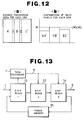
- Fig. 11 shows, as an embodiment of this invention, an example of the image coder of the digital signal processing apparatus.
- input data 1 is entered to a first through third input memories 6.
- a task controller 7 estimates the number of valid pixels on the basis of the contents of the input memory 6, determines the distribution of coding process among a first, second and third DSPs 2, and issues control signals as address control signals 8 to the DSPs 2.
- the first, second, and third DSPs 2 issue addresses 9 to respective first, second and third input memories 6 to fetch data 10 assigned for processing, and implement the coding processes based on the preset program.
- the first, second and third DSPs 2 store processed data in an output memory 11, which, after reading the whole data of the DSP block, sents the processed data to the next DSP block.
- each DSP 2 is controlled by the task controller 7 so that all DSP 2 have even numbers of valid pixels assigned, and therefore the image coding process time is controlled so that the difference of process times among the DSPs 2 is minimal.
- the task controller 7 issues the address control signals 8 corresponding to the assignment distribution to the first, second and third DSPs 2.
- the first DSP 2 in response to the issuance of the address control signal 8 for coding the image data of area A to the first DSP 2, it produces the address 9 for the area A' in the first input memory 6 to fetch data and implements the image coding process by following the prescribed program.
- the second and third DSPs 2 are directed to carry out the image coding processes for the areas B' and C', respectively. Consequently, the first, second and third DSPs 2 have their numbers of valid pixels EA', EB' and EC' for coding virtually made even, i.e., the same quantity of image data to be processed, as shown in Fig. 12(b).
- the maximum volume of process M' dealt with by the inventive apparatus becomes sufficiently less than that M of the conventional apparatus, and the process time required for each DSP block is reduced.
- Fig. 13 shows the inter-frame coder constructed by a serial connection of DSP blocks in three stages.
- Each DSP block performs the process shown in Fig. 14.
- the first DSP block 12 enters upon the input data 1 and, after producing a differential signal, implements the valid/invalid judgment, evaluates the distribution of the numbers of valid pixels in the image data, and sends the information to the task controller 7. Based on the information, the task controller 7 issues address control signals 8 for dictating such address adjustment that the DSPs in the second DSP block 13 have even assignments of data.
- Each DSP in the second DSP block 13 implements the process by adjusting the read address as described above.
- the third DSP block 14 is designed to operate identically.
- the DSP process assignment areas are controlled on the basis of the valid pixel distribution among areas in image data
- the present invention is not confined to this scheme, but feedback DSP assignment control based on the general quantity distribution of transmitted information is also possible, for example.
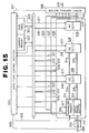
- Fig. 15 shows an example of the configuration of a digital signal processing apparatus, the second embodiment of this invention.
- 301 is a data flow control section (D F C) working as a control means;
- 302 are control parameter data output from the data flow control section 301;
- 303 is a common memory (C M) which stores feedback data, a large capacity data and table, etc.;
- 304 is a task table (T B) which stores a processing status of each signal processor element (P E) 318;
- 305 is a common bus (C-BUS) which has the function as a status communicating means consisting of at least a bus connected to the common memory 303, the task table 304 and each signal processor element 318;
- 306 is a video frame synchronizing signal (F p) which discriminates the starting point of a video frame to be supplied to the data flow control section 301 in the case of inputting video signals etc.;
- 307 are feedback data (F b) which inform the data flow control section
- an output control section 308 is an output control section (O C) provided with a buffer memory for outputting data at a certain constant speed in restructuring processed blocks output from a plurality of signal processor elements (P E) 318 for example in the scanning order in a video frame;
- the data flow control section 301 has a judgment means which scans the task table 304 at a certain constant cycle and judges the processing conditions of individual signal processor elements 318.
- the data flow control section 301 also has a control means which based on the result of the judgment means it decides if each signal processing module can process the next signal process block and when the processing is found to be possible it makes process start by sending out an interruption signal to the interruption control port 317 and when the processing is found to be impossible it instructs the transfer of the signal process block to another signal processing module which can process the block.
- the scanning period shall be the number of parallelness times of the input cycle of the signal process block, and when a series processing is to be done the scanning period shall be l/n of the input cycle; thus by the synchronization with the input data frame (for example a video frame) the matching with the real time can be maintained.
- Fig. 16 shows an example of the internal constitution of the signal processor elements 318 as shown in Fig. 15.
- 330 is a terminal to which the common bus input/output port 316 is to be connected;
- 331 is a terminal to which the interruption control port 317 is to be connected;
- 332 is a terminal to which the buses 314 and 315 are to be connected;
- 333 is similarly a terminal which connects the buses 314 and 315 between the adjacent signal processors;
- 334 is an external bus control section (BUS-CONT) with the function as a competitive control means to control the make/break of the common bus 305 through the bus 316;
- 335 is a bus for loading a writable control storage (W C S) 336, which memorizes a signal processing program, from the external bus control section 334 at an initial time;
- 337 is a BUSREQ which requires the connection of the common bus 305 to the external bus control section 334;
- 338 is a BUSACK which
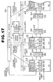
- Fig. 17 explains the internal control operation of the digital signal processing apparatus shown in Fig. 15, and the same parts as those shown in Fig. 15 are given the same symbols; the explanation of them is therefore omitted.
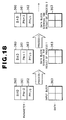
- Fig. 18 explains an example of the relation between the parameter data and process block data until a data block is successively given a series of function processes and an output result is obtained through series and parallel processes of block units executed in the digital signal processing apparatus shown in Fig. 15.
- 360 is a block address (B A D) showing the position of an input block in a frame;
- 361 is a processing number (PN) showing the kind of a process to be given to said block;
- 362 is a flag (PFLG) which discriminates the result of the process;
- 363 is a data block in which for example eight subblocks are combined to form a block.
- Fig. 19 shows an example of correspondence between the data block 363 shown in Fig. 18 and one video frame when a picture coding process is performed in this system.
- 365 is one video frame;
- 366 is a data block when a picture is divided into 16 lines x 16 pixels;
- 367 is a subblock which is obtained when the block is further divided into 8 blocks of 4 lines x 4 pixels.
- Input data 311 digitized by an A/D converter 310 are memorized in an input frame buffer 313 being scanned in a raster form in synchronization with a video frame synchronizing signal 6, for example.
- Input data 311 memorized in the input frame buffer 313 are added to initial parameter data 302 by the data flow control section 301 by blocks and the parameter data 302 are memorized in the parameter memory 312.
- These parameter memory 312 and input frame buffer 313 consist of dual port memories and writing/reading is simultaneously possible between two independent ports.
- Data blocks are read from the input frame buffer 313, and the parameter is read in a data block unit from the parameter memory 312.
- Data blocks and parameter are sent through the buses 314 and 315 to the signal processor 318 element where they are given the first process of a series of functional processes in a block unit.
- the results and the rewritten parameters are written in the dual port memory 349 in the signal processor element 318. It is the basic function of a processor module 320 to execute processes successively between the adjacent signal processor elements 318 and to execute a pipeline processing for each block unit.
- a processing is executed for each block unit, if a feedback data such as coded previous frame data are to be referred to, feedback data are input to the common memory 303 connected to the common bus 305 and memorized.
- the process of a new video frame is performed by such processing that the other signal processor 318 than the one which data have written through common bus 305 refers the common memory 303. If the writing of the feedback data of the previous frame is not completed in the proper position in the common memory 303, the execution time of the process shall be specified.
- each signal processor element 318 When the processing of a unit (block processing) is finished, each signal processor element 318 memorizes the status showing the completion of the present processing in the task table 304, and wait the next processing.
- the data flow control section 301 scans the task table 304 and when the processing of the former stage signal processor element 318 is completed, it sends out an interruption signal to said signal processor element 318 and start the next processing. By repeating the operation, the execution of the operation control of each signal processor element 318 is performed.
- each processor module 320 To conduct parallel processing in a block unit for each processor module 320, the data processing condition in the input frame buffer 313 of each processor module 320 is detected with the status information of the initial stage signal processor 318 and individual block data are distributed by proper load distribution and input to each multi-processor module 320.
- the control parameter data of the initial stage discriminates the processing for the block by deciphering the above results and executes a proper processing.
- processings there are for example functional processors such as a block identifier 253, a coder 254, a local decoder 260, an inter-frame subtracter 252, a motion compensator 265, an inter-frame adder 261, a variable length coder 256, and besides them a processing which performs only load distribution such as a processing of transferring block data is included.
- the output control section 308 reconstitutes processed blocks which are output at random times into for example a scanning order of an input video frame and produces a resultant output for an output terminal 319 and also produces feedback data 307 to inform the data flow control section 301 of these data.
- the output control section 308 takes charge for example of a video multiplex section 257 and a transmitting buffer 258 shown in Fig. 5, and it outputs a feedback signal 269 from the transmitting buffer 258 to a coding control section 270 which takes charge of the data flow control section shown in Fig. 15.
- the data flow control section 301 takes charge of the functions of above-mentioned load distribution and the coding control section 270 as shown in Fig. 5, and finds the block identification control signal 273 and coding control signal 274 and multiplex them in the control parameter data for the execution of the whole characteristic control.
- Fig. 16 the processing of a single signal processor element 318 is started by the interruption from the data flow control section 301, and the contents of the parameter memory 312 is input to it through an internal bus 344.
- the processing of one unit of block data is performed by a digital signal processor 340.
- the result and rewritten parameters are written in a dual port memory 349, and the status is set in the task table 304 through an external bus control section 334; thus the preparation for the next process is ready.
- An interruption control section 345 interfaces the interruption from the data flow control section 301 with the digital signal processor 340.
- the parameter and the data written in the dual port memory 349 are read by an adjacent signal processor element 318 which is connected to a terminal 333, and the next stage process is given.
- Fig. 17 shows the flow of these processes performed by the data flow control section 301, and it shows the relation between the control of writing/referring of feedback data to the common memory 303 and the control of status writing in the task table 304 by the data flow control section 301 through the common bus 305, and the start processing control in the signal processor element 318 by a parameter analyzer 351.
- Fig. 18 shows the rewriting of the contents of control parameter data 302, which are added corresponding to an input block data 363, and the flow of these processes.
- a block address which shows for example the position in a frame or time sequential order of a block, and a flag 362 which is referred to on the kind of the next process and the contents of the next process are contained in the control parameter data 302.
- the block address 360 is used for the discrimination of a special process in a certain case for example with an end point in a picture or for the restructure of data in the output control section 308 when a process is finished.
- the flag 362 shows for example the results etc. of coding control information 271, a block identification control signal 273, coding control signal 274, and a block identifier 253 as shown in Fig.
- Input block data 363 are set to have the minimum size handled in a unit processing.
- the motion compensator 265 shown in Fig. 5 has a block of 16 x 16 size and after the block identifier 253 blocks of 4 x 4 sizes are handled.
- block sizes are arranged to have matching between a maximum block size and a subblock size contained in it.
- eight pieces of 4 x 4 blocks are combined to constitute a 16 x 16 block.
- this block corresponds to a small picture element made by dividing an ordinary one frame into small square picture elements.
- Fig. 19 shows an example where one video frame 365 is divided into a block 366 and subblocks 367.
- a signal processor element 318 which has a single digital signal processor 340, is shown but when a higher speed processing is preferable a hierarchical structure combined with a plural number of digital signal processors can be used.
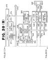
- the constitution of the signal processor element 318 in the case of the hierarchical structure is shown in Fig. 20.
- a local data flow control section 370 As the load for the data flow control section 301 increases a local data flow control section 370, a local common memory 371, and a local task table 372 are provided inside the signal processor 318 in order to locally execute the optimum load distribution inside the signal processor.
- the data flow of the digital signal processor 340 which is connected to a local common bus 373 is the same as that shown in Fig. 15 except that the operation is executed inside the signal processor 318.
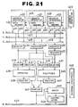
- 420, 421 and 422 are address generators for readout data; 423 is an address generator for writing data; 424, 425 and 426 are data memories, and address data generated by the address generator 423 are input to these memories; 427, 428 and 429 are data buses which transfer readout data from the data memories 424, 425 and 426; 430, 431 and 432 are registers for holding data transferred from data buses 427, 428 and 429; 433 is a register to hold the output of the register 432; 434 is a selector to select the output of the register 430 or that of the register 433; 435 is a selector to select the output of the register 431 or that of the register 441; the selector 434 and the selector 435 constitute a first selector group; 436 is a selector to select the output of the register 430 or the output of a register 439; 437 is a selector to select the output of the register
- top addresses of three series of input data and of an output result storing memory are initially set by address generators 420, 421 and 422. After that the address generators are assumed to take simple increment actions.
- the data memory 424 corresponds to the address generator 420; the data memory 425 corresponds to the address generator 421; the data memory 426 corresponds to the address generator 422. Individual data memories 424, 425 and 426 readout data based on the addresses of address generators 420, 421 and 422.
- Data are input to three data buses 427, 428 and 429 (X-BUS, Y-BUS, Z-BUS) respectively from data memories 424, 425 and 426, so that for the outputting of each of these data memories 424, 425 and 426 to a specified data bus, only one bus out of three is controlled to be effective, and the other two are controlled to be in the state of a high impedance. In this case, the output of data buses is limited to that of the one which is made to be effective.
- the A series data are output to the signal line 451, and the signal lines 461 and 471, which output data from other data memories 425 and 426 to the data bus 427, are in the state of a high impedance. The same thing goes for other data buses.
- Each of these data series are set respectively in the registers 430, 431 and 432.
- Three data buses 427, 428 and 429 can select data from three data memories 424, 425 and 426, so that 33 kinds of data set combinations can be supplied to the registers 430, 431 and 432.
- a selector 434 selects the side of a register 430 and a selector 431 selects the side of a register 435.
- the operation (ai ⁇ bi) is performed with an operator 438, and the result is stored in a register 439. This value is output from the register 439 in the next step.
- the data ci in the register 432 are delayed by the register 433 by one step.
- a selector 436 selects the side of the register 439 and a selector 437 selects the side of a register 433.
- (ai ⁇ bi) is multiplied by ci with the multiplier 440 and the result (ai ⁇ bi) x ci is stored in a register 441.
- This value is output from the register 441 in the next step.
- an output selector 442's selecting the register 441 the data (ai ⁇ bi) x ci are sent to one of the data memories 424, 425 and 426 through a data bus 445 based on the address shown by the address generator 423.
- the selector 434 selects the side of the register 433 and the selector 435 selects the side of the register 441, and the operation (ai x bi) ⁇ ci is executed by the operator 438 and the result is set in the register 439.
- the selector 442's selecting the side of the register 439 the selection result is written into one of the data memories 424 to 426.
- the value of (ai ⁇ bi) can be obtained through the procedure as shown in the following: the selector 434 selects the side of the register 430 and the selector 435 selects the side of the register 431 and after the operation is executed by the operator 438 the side of the register 439 is selected by the selector 442 in the next step.
- the value of (ai x bi) can be obtained through the procedure as shown in the following: the selector 436 selects the side of the register 430 and the selector 437 selects the side of the register 431, and after the execution of the operation with the multiplier 440 the selector 442 selects the side of the register 441 in the next step.
- the processing speed in the case of three input one output is (2N + 10/N + 7) times of that of prior art, that is almost half times if N is a large number.
- Fig. 23 shows a flow chart to realize a method for motion compensative operation which refers to an embodiment of this invention.
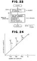
- Fig. 24 is a drawing for the explanation of an intermediate check method in the distortion quantity operation in this invention.
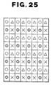
- Fig. 25 is a disposition drawing of a pixel sample at a sample point in a block in the intermediate check method for distortion operation in this invention.
- distortion quantity of all the pixels in the block Before the operation process, on the first block among M pieces of candidate blocks for search in the previous frame data, distortion quantity of all the pixels in the block shall be measured; the distortion quantity in this case is defined to be the minimum distortion.
- the distortion quantity differential absolute value sum is adopted. In the distortion quantity operation about on and after the second block the calculation of differential absolute values of all pixels is not needed, but at an intermediate check point if the intermediate distortion quantity exceeds a certain value, it is judged that the ultimate distortion quantity of the block cannot be smaller than the minimum distortion D and the distortion quantity operation for the residual part is stopped.
- a block which gives the minimum distortion is detected by the calculation of the degree of approximation between the patterns by using the difference and accumulation of pixels in the respective M blocks which are selected out of the present input frame and the previous input frame (M is a positive integer).
- the number of pixels used for the calculation of the degree of approximation is K at the maximum (K is an integer greater than or equal to one and smaller than or equal to the number of a total number of pixels in one block).
- K is an integer greater than or equal to one and smaller than or equal to the number of a total number of pixels in one block).
- the mark ⁇ expresses a first time sample point for distortion quantity operation; the mark x expresses a second time sample point for distortion quantity operation; the mark ⁇ expresses a third time sample point for distortion quantity operation; the mark o expresses a fourth time sample point for distortion quantity operation.
- di1 expresses the value of the first time distortion quantity in Fig. 25; di2 expresses a cumulative value, di1 plus the second time distortion quantity; di3 expresses a cumulative value, di2 plus the third time distortion quantity. Therefore, the cumulative value in which the fourth time distortion quantity is accumulated becomes the distortion quantity in which all sample points are included.
- distortion quantity di3 is performed with the calculation at 3/4 K sample point, and if it is found that di3 > d3' by the judgment in the next step ST46 this block is canceled, if not, the operation is continued into the step ST47 and the distortion quantity di at K sample point is calculated for performing comparison and renewal.
- the same result is obtained as that obtained with the conventional method in which the whole pixels are used for a distortion operation.
- the distortion quantity di in this case, is smaller than the minimum distortion D
- the value of the minimum distortion D is renewed for di
- the motion vector index is renewed for the index i.
- the final minimum value of distortion D and the vector index I which shows the movement to give D can be obtained by repeating such operating processes as mentioned above by the number of times corresponding to the number of searching vectors till the process proceeds up to the Mth block.
- differential absolute value sum is used for distortion quantity operation
- differential square value sum can also be used.
Abstract
Description
- The present invention relates to a digital signal processing apparatus which performs computational processes for digital signals.
- Fig. 1 shows the multiprocessor system described in article entitled "A Real Time Video Signal Processor Suitable for Motion Picture Coding Applications", IEEE, GLOBCOM '87, p. 453. In Fig. 1,
input data 1 is received by adata transfer controller 3, and thereafterdata 4 are transferred selectively todigital signal processors 2, i.e. DSP-1 through DSP-N, in block-1. After being processed by the respective DSPs in block-1,resultant data 5 is transferred to block-2 and processed by respective DSPs for the next processing step. - Fig. 2(a) shows divided memory areas of the DSPs. For the simplicity of explanation, shown here is an example of parallel processing using three
DSPs 2, to which process areas A, B and C are assigned evenly. - In the inter-frame image coding system and the like, it is a general convention to employ the conditional pixel supplementary process in which only portions having at least a certain difference between the input frame and previous frame are coded and previous frame data is used for the remaining portions. Accordingly, the volume of computation needed for the process differs depending on the valid pixel rate even though the number of pixels in the process area is constant. The volume of computation or computation time needed is proportional to the valid pixel rate.
- In the inter-frame image coding system or the like, assuming that the number of valid pixels is shared by all DSPs to have a distribution EA, EB and EC as shown in Fig. 2(b), the computation time needed for one block of parallel DSP configuration is determined from the process time of the DSP which works for the area B with the largest volume of process M, and the remaining DSPs which have finished the areas A and C earlier have idle time.
- The conventional digital signal processing apparatus arranged as described above has its overall process time determined from the longest process time among DSPs when the density of information, such as the valid pixel rate, within a frame is uneven and the distribution of information varies with time, resulting in a degraded process efficiency per DSP unit.
- Fig. 3 is a diagram showing, as an example, the arrangement of other digital signal processing apparatus disclosed in an article entitled "Realtime Video Signal Processor Module", in the proceeding of ICASSP '87, pp. 1961 - 1964, April 1987, Dallas, U.S.A. In the figure, indicated by 1 is an input terminal, 4 is an input bus for distributing input data on the
input terminal input storage 21, aprocessing unit 22, anoutput storage 23 and atiming control unit 24. Indicated by 25 are wired-OR circuits through which feedback data onoutput ports 30 are placed on thefeedback bus output ports 29 are delivered to theoutput terminal 5 over theoutput bus 5a, 27 are input ports for the input data to thesignal processing module signal processing module 20. - Fig. 4 is a block diagram showing in more detail one of the signal processing module in Fig. 3. In the figure, indicated by 221 is an address generator (AGU A), 211 is an input dual memory (MEM A) which receives data on the
input port 27 over theinput bus feedback bus 28a by way of theinput port X-bus 223 and another input terminal EX2 connected to the Y-bus 224. Indicated by 226 is a data memory [MEM P(Q)] having its output connected to theX-bus bus 224 anddata memory X-bus 223 and Y-bus address generators arithmetic unit 225 anddata memory 226. Indicated by 242 is a sequencer (SEQ), 243 is an instruction memory (IRAM) connected to the output of thesequencer 242, and 245 is a decoder (DEC) connected to the output of the instruction memory 243, with the output of thedecoder 245 being connected to the Z-bus 241 andoutput bus 231. Theoutput bus 231 is connected to the input of themode register 228 and the Z-bus 241. Indicated by 232 is an FIFO memory (MEM C) connected to theoutput bus output bus FIFO memory FIFO memory 233. - Fig. 5 is a diagram showing, as an example, the algorism of a typical high-efficiency coder for a moving image. In the figure, indicated by 250 is an input terminal for the input video signal, 251 is an input frame buffer having at least a l-frame capacity and having the simultaneous read-write ability, 252 is an inter-frame subtracter for evaluating the difference, 253 is a block identifier, 254 is a coder, 255 is a coding parameter produced by the
coder input terminal 250 andoutput terminal 259 are the above-mentioned functional blocks 251 - 254 and 256 - 258. Further indicated by 260 is a local decoder which receives thecoding parameter input frame buffer 251 to themotion compensator motion compensator 265 to theinter-frame subtracter 252 andinter-frame adder video multiplexer 257, a feed-forward signal to theinput frame buffer 251, a blockidentification control signal 273 to theblock identifier 253, and a coding control signal 274 to the variable-length coder 256. - Next, the operation of the conventional digital signal processing apparatus will be described in connection with Fig. 3. This apparatus is intended for moving image processing and is based on the division parallel processing system in which a frame is divided into small frames and a
signal processing module 20 is assigned to each of the divided frame areas. - Initially, each
signal processing module 20 operates on the autonomous basis by expending one video frame time to fetch a divided frame area assigned to it among the input data transferred frame-wise in raster scanning over theinput bus 4 and store the data in theinput storage 21. At the same time, if the process result of the previous frame is needed for the current process, it operates by expending one video frame time to fetch data of the assigned area of the frame in the feedback data from theinput port 28 over thefeedback bus 28a and stores the data in theinput storage 21. - Upon expiration of one video frame time, the
processing unit 22 performs the prescribed signal processing for the input data and feedback data stored in theinput storage 21, and stores the result temporarily in theoutput storage 23. The feedback data led out of theoutput storage 23 through theoutput port 30 is timed for synchronization with othersignal processing modules 20 and, by being merged into all feedback data by the wired-OR circuit 25, placed on thefeedback bus 28a. Similarly, the output data led out of theoutput storage 23 through theoutput port 29 is timed for synchronization with othersignal processing modules 20 and, by being merged into all output data by the wired-OR circuit 26, delivered to theoutput terminal 5 over the output bus 5a. - Divided frame areas processed indivisually by the
signal processing modules 20 are combined back to a video frame. Therefore, parallel processing of areas divided type is realized. For reason as described above, it is necessary for allsignal processing modules 20 to have their process commencement in complete synchronism with one another. On this account, thetiming control unit 24 provides all sections of system with the timing of data input/output and process commencement in synchronism with the video frame timing which is the synchronization reference point. - Next, the operation of one
signal processing module 20 will be briefed in connection with Fig. 4. Among a video frame entered frame-wise through theinput port 27 in synchronism with the video frame sync signal, data of the assigned area is stored in the inputdual memory 211. At the same time, among the coded previous frame data entered through theinput port 28, the portion of the assigned area and its peripheral data are stored in the inputdual memory 212. - The input
dual memories X-bus 223 and Y-bus 224 for reading for the coding process by the pipelinearithmetic unit 225. The read/write sides of the inputdual memories input ports - The data read out to the
X-bus 223 and Y-bus 224 are those stored at data memory addresses indicated to the inputdual memories address generators decoder 245 by decoding a 80-bit length horizon-type microcodes read out in accordance with the address of the command memory 243 indicated by the sequencer 242. The data placed on theX-bus 223 and Y-bus 224 are entered in parallel to the pipelinearithmetic unit 225, which implements a series of signal processing including coding and local decoding and outputs the result to the Z-bus 241. Among the process outputs placed on the Z-bus, the coded output is stored in theFIFO memory 232 and the local decoded output is stored in theFIFO memory 233 by way of theoutput bus 231. - The FIFO
memories output ports - The
data memory 226 which is controlled by the output of theaddress generator 227 is used by a work memory which is necessary for the process of the pipelinearithmetic unit 225 and a table which stores constants. Themode register 228 consists of a register file including registers for loading immediate values from thedecoder 245. - This digital signal processing apparatus is principally based on the foregoing area division parallel processing, and is intended such that each
signal processing module 20 deals with a divided frame area independently on a realtime basis. When the digital signal processing apparatus is intended for the achievement of a coder as shown in Fig. 5, only portions excluding the variable-length coder 256,video multiplexer 257,transmission buffer 258 andcoding controller 270 can be realized. Namely, it is not suitable for a continuous process in one video frame, and is limited to the inter-frame coding loop process ranging from theinput frame buffer 251 to theblock identifier 253,coder 254,local decoder 260,coding frame memory 263, and to themotion compensator 265 useful for data completely divisible within a frame. - Since each
signal processing module 20 implements the same process for each frame, the processing program stored in the instruction memory 243 can be a single program. When a frame is divided into M areas (M is an integer greater than or equal to 1), the number of process cycles Nc per pixel which can be dealt with on a realtime basis by onesignal processing module 20 is given by the following calculation.
- On this account, if a frame is divided into four areas, for example, each having the assignment of a
signal processing module 20, the number of process cycles Nc is increased by four fold, and it becomes possible for the video signal processing, which is required to be very fast, to be dealt with on a realtime basis by an increased number of relatively slowsignal processing modules 20. - The conventional digital signal processing apparatus arranged as described above have the following problems for processing video signals.
- (a) For the achievement of very fast processing, a frame must be divided into numerous small areas, however, certain signal process algorism does not allow independent processes for areas below a certain minimal division size. Therefore, realtime processing can not be achieved by increasing the parallelism.
- (b) Because of a fixed distribution of load to signal processing modules, the process time must be set to meet the longest one when each signal processing module has a different process time. Therefore, the system has an unnecessarily increased parallelism relative to the processing capacity.
- (c) Data input and data processing each take one frame time, and data input and output each need a l-frame buffer memory, resulting in a longer time lag and an increased memory capacity. Therefore, the system involves a significant loop delay in feedback control and the like, and it is difficult to realize the
coding controller 270 in Fig. 5 for example. - (d) Since the system is intended for a complete parallel processing, it cannot perform such a process as scanning the entirety of a same frame horizontally.
- Fig. 6 is a block diagram of the conventional digital signal processing system disclosed in the proceeding (No. S10-1) of the 1986 annual convention of the communication department of The Institute of Electronics and Communication Engineers of Japan. In the figure, indicated by 31 is a dual-port internal data memory (will be termed 2P-RAM) capable of reading and writing two sets of data simultaneously, 32 is an address generator which calculates the address of read data or write data, 33 is a data bus used for the internal transfer of data related to computation, 34 and 35 are selectors which select data in the 2P-
RAM selector selector multiplier register 36 or accumulators (ACC0 - ACC3) 44, 41 is a selector which selects the output of theregisters selectors logic unit 42 or data in anexternal data register 46. Theaccumulators 44 are used to hold the output of the arithmetic/logic unit 42 for cumulative computations. The external data register 46 is to hold data from anexternal data memory 47. Indicated by 45 is an external address register which holds address data provided by theaddress generator 32 and transfers it to theexternal data memory 47. - Next, the operation will be described. This signal processing system based on a digital signal processor performs command fetching and decoding for the preset microprogram, data reading, computation, and computation result writing, in a parallel pipeline processing mode. The following describes the operation of 3-input-1-output computation.
- The arithmetic/logic unit, multiplier, address generator, data memories and selectors are controlled in the microcommand mode.
- Arithmetic operations for two inputs, including addition, subtraction, maximum evaluation, minimum evaluation, etc. are expressed generically by a⊕b, and a multiplication operation for two inputs is expressed generically by a x b, where a and b are independent data.
- The arithmetic operations and multiplication are combined to form 3-input-1-output operations, and they are defined by the following expressions.

RAM 31. - Fig. 7 shows the sequence of process for implementing the 3-input operation of the form of expression (1) by the digital signal processing system, for example, shown in Fig. 6.
- The data address
generator 32 sets up the starting addresses for two data sets A and B, and selects the simple incremental mode Then the two data sets A and B are loaded through theselectors registers selectors registers logic unit 42 implements the arithmetic operation ai⊕bi. Theselector 43 selects the arithmetic/logic unit 42 to hold the operation result temporarily in one of accumulators (ACC0 - ACC3) 44, and the resultant data is sent over thedata bus 33 and through theexternal register 46 and stored in theexternal memory 47, which addressing mode is the simple incremental mode because of it being linked to one of addresses for the 2P-RAM 31 in theaddress generator 32. - In the subsequent step ST3, the
data address generator 32 sets up the starting addresses of the data set C and data set ai⊕bi, and ci data is read out of the 2P-RAM 31 to theregister 36. Theselector 35 selects the data bus to load the data of ai⊕bi in theexternal memory 47 into theregister 37. In this case, in order to have a coincident timing of reading for the data set C and data set ai⊕bi, step ST4 needs to expend two cycles of useless command reading for the external memory in advance. - The two sets of data are rendered multiplication by the
multiplier 38 in step ST5, and the result is stored in theregister 39. In the next cycle, the resultant data is passed through the arithmetic/logic unit 42 and, after being held temporarily in one of the accumulators (ACC0 - ACC3) 44, transferred over thedata bus 33 to the 2P-RAM 31. - These operations are carried out in parallel on the basis of the pipeline process, and the operations from the reading of 2P-
RAM 31 until the storing of the process result in theexternal memory 47 for N pieces of data sets will take N + 3 machine cycles in the case of an arithmetic operation. - The steps of operations are listed in the following Table 1 and Table 2. Table 1 is for the operation of ai⊕bi and the transfer of the result to the
external memory 47, and Table 2 is for the reading the resultant ai⊕bi from theexternal memory 47, the operation of (ai⊕bi)·ci, and the transfer of the result to the 2P-RAM. In both tables, symbol "x" represents an indefinite value. Storing in the external data register 46 completes in machine cycle N + 3 in both tables, and the external data register 46 is read uselessly in machine cycle 0 (two machine cycles) in Table 2.

- Next, after two useless reading cycles of the
external memory 47 for timing purposes, multiplication is carried out for N pieces of data sets and the results are stored in the 2P-RAM 31. These operations take N + 3 machine cycles, which are added by two command cycles for address initialization, and a total of 2N + 10 cycles are expended. An operation of expression (2) also takes 2N + 10 cycles. Accordingly, it will be appreciated that if a 3-input-1-output operation is conducted for N pieces data sets using a processor with the ability of 2-input operation at most, it will take about 2N machine cycles (provided that N is sufficiently large). - The following describes the cumulative operation for the results of the foregoing 3-input-1-output computation.

logic unit 42, and the result of summation is entered back to thesame accumulator 44 through theselector 43. Thereby, the process takes 2N + 10 cycles unchanged. - In the case of expression (4), the data sets (ai x bi) ⊕ ci which have been stored temporarily in the 2P-
RAM 31 are read out sequentially and summed by the arithmetic/logic unit 42, and therefore the process needs another N cycles, resulting in a total of 3N + 10 cycles. - The conventional digital signal processing system is formed as described above, and therefore for a 3-input-1-output operation of three independent data sets, it performs two times of 2-input-1-output operation. In addition, the process time is further extended for address control, memory transfer and other processes.
- Fig. 8 is a diagram showing in brief the image coding transmitter which implements the conventional motion compensatory operation method disclosed in an article entitled "Dynamic Multistage Vector Quantization for Images", journal of The Institute of Electronics and Communication Engineers of Japan, Vol. J68-B, No. 1, pp. 68 - 76, Jan. 1985. In the figure, indicated by 1 is an input signal of image data formed of a plurality of consecutive frames on the time axis, 52 is a motion compensator which produces a prediction signal on the basis of the resemblance computation of correlation between the current frame represented by the
input signal 1 and the previous frame represented by aprevious frame signal 53 which is the previous reducedsignal motion compensator 52 indicative of the position of a prediction signal block, 55 is a prediction signal produced by themotion compensator input signal 1 andprediction signal coder decoder 57 and the signal from themotion compensator 52. - The performance of the foregoing arrangement will be described in connection with Fig. 9. The motion compensation process is to calculate for the
input signal 1 the amount of distortion between a 11-by-12 block located in a specific position in the current frame shown in Fig. 9(A) and M pieces of blocks in the search range S in the previous frame shown in Fig. 9(B) to evaluate the position of the block y providing a minimal distortion relative to the position of the input block, i.e., motion vector V, and to recognize the signal of the minimal distortion block as a prediction signal. - The number of motion vectors V under search within the search range S in the given frame is assumed to be M (an integer greater than 1). The amount of distortion of the position of a specific motion vector V between the previous frame blocks and the current input block is calculated as a sum of absolute values of differences as follows.


- These operations must be completed within the period of each frame entered successively, and therefore a high-speed digital signal processor is required.
- As an example, the digital signal processing system shown in Fig. 6 is used to carry out the motion compensation process. In this case, the multiplication-sum operation takes place K x M times for each input block, and the number of machine cycles is the total time expended by M times of processes including comparison and updating. Generally, the number of cycles for comparison and updating is small enough as compared with that of the multiplication-sum operation, and the volume of motion compensation operation for one block is virtually equal to K x M machine cycles.
- However, since these operations are determined from the time corresponding to the period of frames entered successively, parallel processing will be needed for the mass multiplication-sum operations to be performed in a short time, depending on the operation process cycle time of a particular digital signal processor.
- The conventional motion compensation scheme is implemented as described above, and in order to ensure the operation time for an enormous volume of operations when carried out using a digital signal processor, the processor needs to have parallel processings, resulting in an increased complexity and scale of hardware structure.
- The present invention is intended to overcome the foregoing prior art deficiencies, and a prime object to provide a digital signal processing apparatus which uses the multiprocessor parallel configuration to its maximal processing ability.
- Another object of this invention is to provide a digital signal processing apparatus which works efficiently with less number of processors and less capacity of memory, while ensuring the latitude of signal processing algorism.
- Still another object of this invention is to provide a digital signal processing apparatus which eliminates the need of address control for storing the intermediate result and transfer to the memory, thereby executing fast 3-input-1-output operation.
- A further object of this invention is to provide a motion compensative operation method which, in constructing the motion compensator of an image coding system with a digital signal processing apparatus, requires less number of parallel processors, thereby enhancing the simplicity and compactness of the hardware structure.
- In order to achieve the above objectives, the inventive digital signal processing apparatus comprises a plurality of processors and a task controller which issues address control signals of task assignment to the processors so that they fetch an even quantity of significant information to their memories for processing.
- Furthermore, the inventive digital signal processing apparatus comprise a plurality of signal processors connected with one another through a dual-port memory arranged in series and/or parallel, a shared memory which can be accessed for reading and writing in blocks of signal processing or in arbitrary number of data from all of the signal processors, a task table which stores the process status in the signal processors, and a data flow controller which scans the contents of the task table at a certain interval, determines a charged process of each signal processor on the basis of feedback data including the occupancy rate of buffer memory reported by the output controller, and directs the interrupt controller of each signal processor to start.
- Furthermore, the inventive digital signal processing apparatus comprises a first through third data reading address generators adapted to read three independent data sets independently and simultaneously, and a pair of arithmetic unit and multiplier adapted to execute a 3-input-1-output arithmetic operation at high speed by receiving the output of counterpart mutually.
- The inventive motion compensation method using a digital signal processing apparatus divides a current input frame of digital image data, which consists of a plurality of frames, entered successively into a plurality of blocks, searches the previous input frame for a pattern which resembles the block of the input frame, and implements a coding process with a block of minimal distortion in highest resemblance as a prediction signal, wherein in detecting a block of minimal distortion through the computation of inter-pattern resemblance using the difference and cumulation of pixels in each block between the block of the current input frame and blocks of M in number (M is a positive integer) in the previous input frame, the method uses, for the pattern resemblance computation, a maximum of K pieces of pixels (K is an integer greater than 0 and less than or equal to a total number of pixels in a block), implements an intermediate check n times (n is an integer greater than 0) during the computation of resemblance at time points when the number of reference pixels is smaller than K, skips the computation for remaining pixels when a cumulative value at each time point of intermediate check is greater than a threshold value which is set for each time point of intermediate check and excludes the block from the range of comparison for finding a minimal distortion block, and detects by computation the minimal distortion block among blocks in which cumulative values are below the thresholds at all time points of intermediate check.
-
- Fig. 1 is a block diagram showing the multiprocessor system of a conventional digital signal processing apparatus;
- Fig. 2 is a diagram explaining the assigned areas of the processors shown in Fig. 1;
- Fig. 3 is a block diagram showing the arrangement of other conventional digital signal processing apparatus;
- Fig. 4 is a block diagram showing in detail the arrangement of the signal processing module shown in Fig. 3;
- Fig. 5 is a block diagram showing the algorism of the high-efficiency coder for a moving image;
- Fig. 6 is a block diagram showing the arrangement of a third conventional digital signal processing apparatus;
- Fig. 7 is a flowchart showing the process of 3-input arithmetic operation using the digital signal processing apparatus shown in Fig. 6;
- Fig. 8 is a block diagram showing in brief the arrangement of the image coding transmitter which carries out the conventional motion compensative operation method;
- Fig. 9 is a diagram used to explain the conventional motion compensative operation method;
- Fig. 10 is a flowchart showing the operational process for detecting a motion vector in the conventional motion compensative operation method;
- Fig. 11 is a block diagram showing the digital signal processing apparatus based on the first embodiment of this invention;
- Fig. 12 is a diagram explaining the area assignment for the processors shown in Fig. 11;
- Fig. 13 is a block diagram showing the arrangement of the digital signal processing apparatus formed by connecting in cascades a plurality of digital signal processors (DSP blocks) shown in Fig. 11;
- Fig. 14 is a diagram showing the concept of process of each DSP block shown in Fig. 13;
- Fig. 15 is a block diagram showing the digital signal processing apparatus based on the second embodiment of this invention;
- Fig. 16 is a block diagram showing the internal arrangement of the signal processor shown in Fig. 15;
- Fig. 17 is a diagram explaining the concept of control operation of the digital signal processing apparatus shown in Fig. 15;
- Fig. 18 is a diagram explaining the relation between parameter data and processing block data in the digital signal processing apparatus shown in Fig. 15;
- Fig. 19 is a diagram showing the correspondence between data blocks and a frame;
- Fig. 20 is a block diagram of the arrangement in which a plurality of digital signal processors are included in the digital signal processing apparatus shown in Fig. 15;
- Fig. 21 is a block diagram showing the digital signal processing apparatus based on another embodiment of this invention;
- Fig. 22 is a flowchart showing the operational process of the digital signal processing apparatus shown in Fig. 21;
- Fig. 23 is a flowchart showing an embodiment of the inventive motion compensative operation method using a digital signal processing apparatus;
- Fig. 24 is a diagram used to explain the method of intermediate check for the computation of distortion in the inventive motion compensative operation method; and
- Fig. 25 is a diagram showing the arrangement of pixel samples at sampling points in a block according to the intermediate check method for the distortion computation.
- Specific embodiments of the present invention will now be described with reference to the drawings.
- Fig. 11 shows, as an embodiment of this invention, an example of the image coder of the digital signal processing apparatus. In the figure,
input data 1 is entered to a first throughthird input memories 6. Atask controller 7 estimates the number of valid pixels on the basis of the contents of theinput memory 6, determines the distribution of coding process among a first, second andthird DSPs 2, and issues control signals asaddress control signals 8 to theDSPs 2. Upon receiving theaddress control signals 8, the first, second, andthird DSPs 2 issue addresses 9 to respective first, second andthird input memories 6 to fetchdata 10 assigned for processing, and implement the coding processes based on the preset program. Upon completion of processes, the first, second andthird DSPs 2 store processed data in anoutput memory 11, which, after reading the whole data of the DSP block, sents the processed data to the next DSP block. - In this case, each
DSP 2 is controlled by thetask controller 7 so that allDSP 2 have even numbers of valid pixels assigned, and therefore the image coding process time is controlled so that the difference of process times among theDSPs 2 is minimal. Namely, in case of coding an image with numbers of valid pixels as shown in Fig. 12(b), an area A having a relatively small number of valid pixels is enlarged to A', an area C having a relatively large number of valid pixels is also enlarged to C', and an area B having a larger number of valid pixels is reduced to B', as shown in Fig. 12(a), by thetask controller 7. Thetask controller 7 issues theaddress control signals 8 corresponding to the assignment distribution to the first, second andthird DSPs 2. - For example, in response to the issuance of the
address control signal 8 for coding the image data of area A to thefirst DSP 2, it produces theaddress 9 for the area A' in thefirst input memory 6 to fetch data and implements the image coding process by following the prescribed program. Similarly, the second andthird DSPs 2 are directed to carry out the image coding processes for the areas B' and C', respectively. Consequently, the first, second andthird DSPs 2 have their numbers of valid pixels EA', EB' and EC' for coding virtually made even, i.e., the same quantity of image data to be processed, as shown in Fig. 12(b). As a result, the maximum volume of process M' dealt with by the inventive apparatus becomes sufficiently less than that M of the conventional apparatus, and the process time required for each DSP block is reduced. - Fig. 13 shows the inter-frame coder constructed by a serial connection of DSP blocks in three stages. Each DSP block performs the process shown in Fig. 14. The
first DSP block 12 enters upon theinput data 1 and, after producing a differential signal, implements the valid/invalid judgment, evaluates the distribution of the numbers of valid pixels in the image data, and sends the information to thetask controller 7. Based on the information, thetask controller 7 issues addresscontrol signals 8 for dictating such address adjustment that the DSPs in thesecond DSP block 13 have even assignments of data. Each DSP in thesecond DSP block 13 implements the process by adjusting the read address as described above. Thethird DSP block 14 is designed to operate identically. - Although in the foregoing embodiment the DSP process assignment areas are controlled on the basis of the valid pixel distribution among areas in image data, the present invention is not confined to this scheme, but feedback DSP assignment control based on the general quantity distribution of transmitted information is also possible, for example.
- A second embodiment of this invention will be explained with reference to the drawings. Fig. 15 shows an example of the configuration of a digital signal processing apparatus, the second embodiment of this invention. In the figure, 301 is a data flow control section (D F C) working as a control means; 302 are control parameter data output from the data flow control section 301; 303 is a common memory (C M) which stores feedback data, a large capacity data and table, etc.; 304 is a task table (T B) which stores a processing status of each signal processor element (P E) 318; 305 is a common bus (C-BUS) which has the function as a status communicating means consisting of at least a bus connected to the common memory 303, the task table 304 and each signal processor element 318; 306 is a video frame synchronizing signal (F p) which discriminates the starting point of a video frame to be supplied to the data flow control section 301 in the case of inputting video signals etc.; 307 are feedback data (F b) which inform the data flow control section 301 of the occupying status, data quantity of a sending buffer etc. and finishing of one frame data processing etc. output from an output control section 308 described later; 308 is an output control section (O C) provided with a buffer memory for outputting data at a certain constant speed in restructuring processed blocks output from a plurality of signal processor elements (P E) 318 for example in the scanning order in a video frame; 309 is an input terminal of analog signals; 310 is an A/D converter; 311 are digitized input data; 312 is a parameter memory (P M) consisting of dual port memories; 313 is an input frame buffer consisting of dual port memories for functioning as a block formation means by memorizing input data 311 temporarily; 314 is a bus connecting the parameter memory 312 to the signal processor elements 318; 315 is a bus connecting the input frame buffer 313 to the signal processor elements 318 in order to supply data in a block unit; 316 is a common bus input/output port connected to the common bus 305; 317 is an interruption control port for sending/receiving timing control signals from the data flow control section 301; 318 are individual signal processor elements (P E) and these signal processor elements are provided with software which functions as a starting means, and these signal processor elements are mutually connected with buses 314 and 315, and said last stage signal processor element 318 and the output control section 308 are also connected with buses 314 and 315; 319 is an output terminal through which data are output at a certain constant speed and timing from the output control section 308; 320 is a multiprocessor module comprising the parameter memory 312, the input frame buffer 313 and a plurality of signal processors 318 connected in series through the buses 314 and 315, for example.
- The data
flow control section 301 has a judgment means which scans the task table 304 at a certain constant cycle and judges the processing conditions of individualsignal processor elements 318. The dataflow control section 301 also has a control means which based on the result of the judgment means it decides if each signal processing module can process the next signal process block and when the processing is found to be possible it makes process start by sending out an interruption signal to theinterruption control port 317 and when the processing is found to be impossible it instructs the transfer of the signal process block to another signal processing module which can process the block. When a parallel processing of a constant cycle, in which the task table 304 is scanned, is to be done the scanning period shall be the number of parallelness times of the input cycle of the signal process block, and when a series processing is to be done the scanning period shall be l/n of the input cycle; thus by the synchronization with the input data frame (for example a video frame) the matching with the real time can be maintained. - Fig. 16 shows an example of the internal constitution of the
signal processor elements 318 as shown in Fig. 15. In the figure, 330 is a terminal to which the common bus input/output port 316 is to be connected; 331 is a terminal to which the interruption control port 317 is to be connected; 332 is a terminal to which the buses 314 and 315 are to be connected; 333 is similarly a terminal which connects the buses 314 and 315 between the adjacent signal processors; 334 is an external bus control section (BUS-CONT) with the function as a competitive control means to control the make/break of the common bus 305 through the bus 316; 335 is a bus for loading a writable control storage (W C S) 336, which memorizes a signal processing program, from the external bus control section 334 at an initial time; 337 is a BUSREQ which requires the connection of the common bus 305 to the external bus control section 334; 338 is a BUSACK which denotes the permission for the BUSREQ 337; 339 are command codes which are successively read out from the writable control storage 336 according to the signal processing program; 340 is a digital signal processor (D S P) which execute data processing; 341 is an INTACK which informs an interruption control section (INTER-CONT) 345 of the reception of an interruption from the digital signal processor 340; 342 is, on the contrary to it, an INTREQ which informs the digital signal processor 340 of the requirement of an interruption; 343 is a bus to connect an internal bus 344 to the common bus 305 through the external bus control section 334, and the internal bus 344 is directly connected to the digital signal processor 340; 345 is an interruption control section (INTR-CONT) which processes an interruption signal from the data flow control section 301; 346 is a bus which writes the parameter of a processed data block on a dual port memory 349 through the internal bus 344; 347 is similarly a bus which writes processed block on the dual port memory 349; 348 is a bus which connects a work memory in the dual port memory 349 and the internal bus 344; 349 is a dual port memory provided with a parameter memory, data memory and work memory which outputs data to the adjacent signal processor element 318 through the terminal 333 and buses 314 and 315. - Fig. 17 explains the internal control operation of the digital signal processing apparatus shown in Fig. 15, and the same parts as those shown in Fig. 15 are given the same symbols; the explanation of them is therefore omitted.
- In the figure, 351 is a block which shows analytical operation of a parameter inside the
signal processor element 318; 352, 353, 354 are blocks which show the operation of individual signal processing subroutines A, B and C according to the parameter of each of them; 355 is a block which shows the contents of a parameter memorized in thedual port memory 349; 356 is a block which shows the contents D of processed block data memorized in thedual port memory 349. - Fig. 18 explains an example of the relation between the parameter data and process block data until a data block is successively given a series of function processes and an output result is obtained through series and parallel processes of block units executed in the digital signal processing apparatus shown in Fig. 15. In the figure, 360 is a block address (B A D) showing the position of an input block in a frame; 361 is a processing number (PN) showing the kind of a process to be given to said block; 362 is a flag (PFLG) which discriminates the result of the process; 363 is a data block in which for example eight subblocks are combined to form a block.
- Fig. 19 shows an example of correspondence between the data block 363 shown in Fig. 18 and one video frame when a picture coding process is performed in this system. In the figure, 365 is one video frame; 366 is a data block when a picture is divided into 16 lines x 16 pixels; 367 is a subblock which is obtained when the block is further divided into 8 blocks of 4 lines x 4 pixels.
- An explanation of the operation based on Fig. 15 is given in the following.
Input data 311 digitized by an A/D converter 310 are memorized in aninput frame buffer 313 being scanned in a raster form in synchronization with a videoframe synchronizing signal 6, for example.Input data 311 memorized in theinput frame buffer 313 are added toinitial parameter data 302 by the dataflow control section 301 by blocks and theparameter data 302 are memorized in theparameter memory 312. Theseparameter memory 312 andinput frame buffer 313 consist of dual port memories and writing/reading is simultaneously possible between two independent ports. - Data blocks are read from the
input frame buffer 313, and the parameter is read in a data block unit from theparameter memory 312. Data blocks and parameter are sent through thebuses signal processor 318 element where they are given the first process of a series of functional processes in a block unit. Next, the results and the rewritten parameters are written in thedual port memory 349 in thesignal processor element 318. It is the basic function of aprocessor module 320 to execute processes successively between the adjacentsignal processor elements 318 and to execute a pipeline processing for each block unit. - When a processing is executed for each block unit, if a feedback data such as coded previous frame data are to be referred to, feedback data are input to the
common memory 303 connected to thecommon bus 305 and memorized. The process of a new video frame is performed by such processing that theother signal processor 318 than the one which data have written throughcommon bus 305 refers thecommon memory 303. If the writing of the feedback data of the previous frame is not completed in the proper position in thecommon memory 303, the execution time of the process shall be specified. - When the processing of a unit (block processing) is finished, each
signal processor element 318 memorizes the status showing the completion of the present processing in the task table 304, and wait the next processing. The dataflow control section 301 scans the task table 304 and when the processing of the former stagesignal processor element 318 is completed, it sends out an interruption signal to saidsignal processor element 318 and start the next processing. By repeating the operation, the execution of the operation control of eachsignal processor element 318 is performed. - To conduct parallel processing in a block unit for each
processor module 320, the data processing condition in theinput frame buffer 313 of eachprocessor module 320 is detected with the status information of the initialstage signal processor 318 and individual block data are distributed by proper load distribution and input to eachmulti-processor module 320. - These results are shown by the control parameter data of the initial stage and the
signal processor element 318 discriminates the processing for the block by deciphering the above results and executes a proper processing. Among these processings there are for example functional processors such as ablock identifier 253, acoder 254, alocal decoder 260, aninter-frame subtracter 252, amotion compensator 265, aninter-frame adder 261, avariable length coder 256, and besides them a processing which performs only load distribution such as a processing of transferring block data is included. - In the data
flow control section 301, it is possible to make anarbitrary signal processor 318 undertake an arbitrary processing by controlling the first stage parameter; owing to such performance as mentioned above the load can be so distributed to signalprocessor elements 318 as to make them work efficiently as much as possible. - The
output control section 308 reconstitutes processed blocks which are output at random times into for example a scanning order of an input video frame and produces a resultant output for anoutput terminal 319 and also producesfeedback data 307 to inform the dataflow control section 301 of these data. - The
output control section 308 takes charge for example of avideo multiplex section 257 and a transmittingbuffer 258 shown in Fig. 5, and it outputs afeedback signal 269 from the transmittingbuffer 258 to acoding control section 270 which takes charge of the data flow control section shown in Fig. 15. - The data
flow control section 301 takes charge of the functions of above-mentioned load distribution and thecoding control section 270 as shown in Fig. 5, and finds the blockidentification control signal 273 and coding control signal 274 and multiplex them in the control parameter data for the execution of the whole characteristic control. Refer to Fig. 16; the processing of a singlesignal processor element 318 is started by the interruption from the dataflow control section 301, and the contents of theparameter memory 312 is input to it through aninternal bus 344. On the basis of the discrimination result of the contents, the processing of one unit of block data is performed by adigital signal processor 340. - The result and rewritten parameters are written in a
dual port memory 349, and the status is set in the task table 304 through an externalbus control section 334; thus the preparation for the next process is ready. Aninterruption control section 345 interfaces the interruption from the dataflow control section 301 with thedigital signal processor 340. The parameter and the data written in thedual port memory 349 are read by an adjacentsignal processor element 318 which is connected to a terminal 333, and the next stage process is given. - Fig. 17 shows the flow of these processes performed by the data
flow control section 301, and it shows the relation between the control of writing/referring of feedback data to thecommon memory 303 and the control of status writing in the task table 304 by the dataflow control section 301 through thecommon bus 305, and the start processing control in thesignal processor element 318 by a parameter analyzer 351. - Fig. 18 shows the rewriting of the contents of
control parameter data 302, which are added corresponding to aninput block data 363, and the flow of these processes. A block address which shows for example the position in a frame or time sequential order of a block, and aflag 362 which is referred to on the kind of the next process and the contents of the next process are contained in thecontrol parameter data 302. Theblock address 360 is used for the discrimination of a special process in a certain case for example with an end point in a picture or for the restructure of data in theoutput control section 308 when a process is finished. Theflag 362 shows for example the results etc. ofcoding control information 271, a blockidentification control signal 273, coding control signal 274, and ablock identifier 253 as shown in Fig. 5.Input block data 363 are set to have the minimum size handled in a unit processing. Themotion compensator 265 shown in Fig. 5 has a block of 16 x 16 size and after theblock identifier 253 blocks of 4 x 4 sizes are handled. In such a case as mentioned above where a block size differs for each unit processing, block sizes are arranged to have matching between a maximum block size and a subblock size contained in it. In this case, eight pieces of 4 x 4 blocks are combined to constitute a 16 x 16 block. When coding of a picture is performed, this block corresponds to a small picture element made by dividing an ordinary one frame into small square picture elements. - Fig. 19 shows an example where one
video frame 365 is divided into ablock 366 andsubblocks 367. - In the above embodiment, a
signal processor element 318, which has a singledigital signal processor 340, is shown but when a higher speed processing is preferable a hierarchical structure combined with a plural number of digital signal processors can be used. The constitution of thesignal processor element 318 in the case of the hierarchical structure is shown in Fig. 20. In this case, as the load for the dataflow control section 301 increases a local dataflow control section 370, a localcommon memory 371, and a local task table 372 are provided inside thesignal processor 318 in order to locally execute the optimum load distribution inside the signal processor. The data flow of thedigital signal processor 340 which is connected to a localcommon bus 373 is the same as that shown in Fig. 15 except that the operation is executed inside thesignal processor 318. - In the above embodiment, a series/parallel structure is adopted but in some case a complete parallel or complete series structure is effective according to the purpose of a signal processing and a real time processing could be possible.
- The other embodiment of this invention is explained with reference to Fig. 21. In Fig. 21, 420, 421 and 422 are address generators for readout data; 423 is an address generator for writing data; 424, 425 and 426 are data memories, and address data generated by the address generator 423 are input to these memories; 427, 428 and 429 are data buses which transfer readout data from the data memories 424, 425 and 426; 430, 431 and 432 are registers for holding data transferred from data buses 427, 428 and 429; 433 is a register to hold the output of the register 432; 434 is a selector to select the output of the register 430 or that of the register 433; 435 is a selector to select the output of the register 431 or that of the register 441; the selector 434 and the selector 435 constitute a first selector group; 436 is a selector to select the output of the register 430 or the output of a register 439; 437 is a selector to select the output of the register 431 or the output of the register 433; the selector 436 and the selector 437 constitute a second selector group; 438 is an operator which operates by inputting the output of the selectors 434 and 435; 440 is a multiplier which performs multiplication by inputting the output of selectors 436 and 437; the register 439 is the one to hold the output of the operator 438; a register 441 is the one to hold the output of the multiplier 440; 442 is a selector which selects the input from the register 439 or the input from the register 441 and outputs it; 443 is an adder which adds the output of the output selector 442 and the output of an accumulator 444 and outputs to said accumulator 444; 445 is a data bus to transfer output data of the accumulator 444 and the output selector 442; 446 is an interface circuit which performs outputting/inputting of data to/from external circuits; 451 - 453, 461 - 463, 471 - 473 denote signal lines which output the output of data memories 424, 425 and 426 to data buses 427, 428 and 429.
- The following are the explanation of operation. In Fig. 21, assume that data series with N elements,


data memory 424,data memory 425, anddata memory 426. - Under the conditions above, the operation when the operation of three inputs and one output is performed is shown below. The operation processing flow is shown in Fig. 22.
- To begin with, at a step ST31, top addresses of three series of input data and of an output result storing memory are initially set by
address generators - The
data memory 424 corresponds to theaddress generator 420; thedata memory 425 corresponds to theaddress generator 421; thedata memory 426 corresponds to the address generator 422.Individual data memories address generators - Data are input to three
data buses data memories data memories register 430, the A series data are output to thesignal line 451, and thesignal lines 461 and 471, which output data fromother data memories data bus 427, are in the state of a high impedance. The same thing goes for other data buses. - Each of these data series are set respectively in the
registers data buses data memories registers - Two expressions as shown below are defined in the way of three input operation and then the processing method is shown in the following:


- At a step ST32 a
selector 434 selects the side of aregister 430 and aselector 431 selects the side of aregister 435. By the use of these two selected data (ai and bi) the operation (ai ⊕ bi) is performed with anoperator 438, and the result is stored in aregister 439. This value is output from theregister 439 in the next step. - The data ci in the
register 432 are delayed by theregister 433 by one step. In the next step aselector 436 selects the side of theregister 439 and aselector 437 selects the side of aregister 433. By the use of these two data, (ai ⊕ bi) is multiplied by ci with themultiplier 440 and the result (ai ⊕ bi) x ci is stored in aregister 441. This value is output from theregister 441 in the next step. By anoutput selector 442's selecting theregister 441, the data (ai ⊕ bi) x ci are sent to one of thedata memories data bus 445 based on the address shown by theaddress generator 423. - In this invention, readout of data, execution of operation and writing of data are continuously executed by a pipeline processing, so that the control of each section can be operated in parallel. Therefore if the three input one output operation is executed for a data series with N elements, from the time when the first datum is readout until the time when the processing result of the last datum is written into a memory, the period of (N + 3) cycles are required.
- The explanation of operation processing flow of expression (8) is given in Table 4. The mark "x" in Table 4 represents an unknown.

- The operation in which three input data are readout to
registers selector 436 selects the side of theregister 430 and theselector 437 selects the side of theregister 431, and the operation (ai x bi) is performed by themultiplier 440 and the result is set in theregister 441. - In the next step, the
selector 434 selects the side of theregister 433 and theselector 435 selects the side of theregister 441, and the operation (ai x bi) ⊕ ci is executed by theoperator 438 and the result is set in theregister 439. In the next step, by theselector 442's selecting the side of theregister 439 the selection result is written into one of thedata memories 424 to 426. - Thus the case of the operation of expression (8) is the same as the case of expression (7), thereby the total processing time requires (N + 3) cycles.
- In the case of the operation of two input one output, the value of (ai ⊕ bi) can be obtained through the procedure as shown in the following: the
selector 434 selects the side of theregister 430 and theselector 435 selects the side of theregister 431 and after the operation is executed by theoperator 438 the side of theregister 439 is selected by theselector 442 in the next step. The value of (ai x bi) can be obtained through the procedure as shown in the following: theselector 436 selects the side of theregister 430 and theselector 437 selects the side of theregister 431, and after the execution of the operation with themultiplier 440 theselector 442 selects the side of theregister 441 in the next step. - The processing speed in the case of three input one output is (2N + 10/N + 7) times of that of prior art, that is almost half times if N is a large number.
- When a cumulative value is to be found in the three input one output operation, a cumulative value till a point on the way or an initial value is stored in the
accumulator 444 and each one of the successive operation results is added to the cumulative value in theaccumulator 444 with theadder 443 and the added result is stored in theaccumulator 444 again. These processes are performed repeatedly. Processing cycles therefore are not increased due to cumulative operation. - Fig. 23 shows a flow chart to realize a method for motion compensative operation which refers to an embodiment of this invention. Fig. 24 is a drawing for the explanation of an intermediate check method in the distortion quantity operation in this invention. Fig. 25 is a disposition drawing of a pixel sample at a sample point in a block in the intermediate check method for distortion operation in this invention.
- Before the operation process, on the first block among M pieces of candidate blocks for search in the previous frame data, distortion quantity of all the pixels in the block shall be measured; the distortion quantity in this case is defined to be the minimum distortion. As for the distortion quantity, differential absolute value sum is adopted. In the distortion quantity operation about on and after the second block the calculation of differential absolute values of all pixels is not needed, but at an intermediate check point if the intermediate distortion quantity exceeds a certain value, it is judged that the ultimate distortion quantity of the block cannot be smaller than the minimum distortion D and the distortion quantity operation for the residual part is stopped.
- A block which gives the minimum distortion is detected by the calculation of the degree of approximation between the patterns by using the difference and accumulation of pixels in the respective M blocks which are selected out of the present input frame and the previous input frame (M is a positive integer). The number of pixels used for the calculation of the degree of approximation is K at the maximum (K is an integer greater than or equal to one and smaller than or equal to the number of a total number of pixels in one block). During the calculation of the degree of approximation at the time when the number of pixels in reference is less than K intermediate checks are performed four times, and an intermediate check point shall be provided in each 1/4 sample point. Fig. 25 shows examples of sample points used for distortion quantity operation. The mark ○ expresses a first time sample point for distortion quantity operation; the mark x expresses a second time sample point for distortion quantity operation; the mark △ expresses a third time sample point for distortion quantity operation; the mark ⓞ expresses a fourth time sample point for distortion quantity operation.
- In Fig. 24 when the total number of sample points is assumed to be K, express threshold levels at a first, second and third intermediate check points as d1', d2' and d3'; then put

- In this case, di1 expresses the value of the first time distortion quantity in Fig. 25; di2 expresses a cumulative value, di1 plus the second time distortion quantity; di3 expresses a cumulative value, di2 plus the third time distortion quantity. Therefore, the cumulative value in which the fourth time distortion quantity is accumulated becomes the distortion quantity in which all sample points are included.
- On the basis of a distortion quantity judgment at an intermediate check point if a block is estimated to have a large distortion quantity, the checking of the block is canceled before the block reaches the last check point to save useless operation processes. In other words if a distortion quantity di1 which is obtained by a distortion calculation at 1/4 K sample point in a step ST41 is found to be di1 > d1' by the judgment in the next step ST42, the block is canceled, if not, the operation is continued to the next step ST43 and the operation of distortion quantity di2 is performed with the distortion calculation at 1/2 K sample point. If it is found that di2 > d2' in the judgment in the next step ST44 the block is canceled and if not, the operation is continued into the step ST45. The operation of distortion quantity di3 is performed with the calculation at 3/4 K sample point, and if it is found that di3 > d3' by the judgment in the next step ST46 this block is canceled, if not, the operation is continued into the step ST47 and the distortion quantity di at K sample point is calculated for performing comparison and renewal.
- As shown in the above if the processing is performed till the last step the same result is obtained as that obtained with the conventional method in which the whole pixels are used for a distortion operation. If the distortion quantity di, in this case, is smaller than the minimum distortion D, the value of the minimum distortion D is renewed for di and the motion vector index is renewed for the index i. The final minimum value of distortion D and the vector index I which shows the movement to give D can be obtained by repeating such operating processes as mentioned above by the number of times corresponding to the number of searching vectors till the process proceeds up to the Mth block.
- In the above embodiment, the example where differential absolute value sum is used for distortion quantity operation is shown, but differential square value sum can also be used.
- In the above embodiment, explanation is made about the case of motion compensative operation, but the execution of inner product vector quantization operation is also possible and the same effect can be obtained. When an operation result is compared with a threshold value at an intermediate check point, the relation in magnitude is opposite to what is mentioned in the above embodiment.
Claims (2)
- A digital signal processing apparatus comprising a first through third address generators which generate independently addresses for read data; a fourth address generator which generates write address information indicative of a write data destination and address; a first through third data memory, from which data are read out in accordance with addresses of said first through third address generators and to which data are written in accordance with address information of said fourth address generator; an operator which performs an arithmetic/logic operation for a pair of data selected by a first selector group under control of microprogram from among a first data pair consisting of data of said first data memory and data of said second data memory and a second data pair consisting of data of said third data memory and output data of a multiplier; a second selector group which selects one of said first data pair, and a third data pair consisting of data of said third data memory and output data of said operator under control of said microprogram so that a selected data pair is subjected to a multiplication operation by said multiplier; an output selector which selects one of the output of said operator and the output of said multiplier and transfers the selected output data over a data bus to said first data through third data memories or an external circuit; and an accumulator which provides an output for the addition operation by an adder for cumulation of output value, holds cumulatively the result of addition by said adder, and transfers the output as write data to said first through third data memories or an external circuit.
- A digital signal processing apparatus according to claim 1, wherein said first through third address generators have an auto-increment mode for addressing.
Applications Claiming Priority (13)
| Application Number | Priority Date | Filing Date | Title |
|---|---|---|---|
| JP37921/88 | 1988-02-19 | ||
| JP3792188 | 1988-02-19 | ||
| JP63037921A JPH01211162A (en) | 1988-02-19 | 1988-02-19 | Real time multi-processor-type signal processor |
| JP63695/88 | 1988-03-18 | ||
| JP63063695A JPH01237838A (en) | 1988-03-18 | 1988-03-18 | Digital signal processing system |
| JP6369588 | 1988-03-18 | ||
| JP29872388 | 1988-11-26 | ||
| JP29872288 | 1988-11-26 | ||
| JP298723/88 | 1988-11-26 | ||
| JP63298722A JPH02145079A (en) | 1988-11-26 | 1988-11-26 | Movement compensated calculation method |
| JP63298723A JPH02145077A (en) | 1988-11-26 | 1988-11-26 | Information encoder |
| JP298722/88 | 1988-11-26 | ||
| EP19890102717 EP0329151A3 (en) | 1988-02-19 | 1989-02-17 | Digital signal processing apparatus |
Related Parent Applications (2)
| Application Number | Title | Priority Date | Filing Date |
|---|---|---|---|
| EP19890102717 Division EP0329151A3 (en) | 1988-02-19 | 1989-02-17 | Digital signal processing apparatus |
| EP89102717.9 Division | 1989-02-17 |
Publications (2)
| Publication Number | Publication Date |
|---|---|
| EP0703533A1 true EP0703533A1 (en) | 1996-03-27 |
| EP0703533B1 EP0703533B1 (en) | 1999-11-17 |
Family
ID=27460495
Family Applications (3)
| Application Number | Title | Priority Date | Filing Date |
|---|---|---|---|
| EP95114933A Expired - Lifetime EP0703533B1 (en) | 1988-02-19 | 1989-02-17 | Digital signal processing apparatus |
| EP19890102717 Withdrawn EP0329151A3 (en) | 1988-02-19 | 1989-02-17 | Digital signal processing apparatus |
| EP95114932A Expired - Lifetime EP0690376B1 (en) | 1988-02-19 | 1989-02-17 | Digital signal processing method |
Family Applications After (2)
| Application Number | Title | Priority Date | Filing Date |
|---|---|---|---|
| EP19890102717 Withdrawn EP0329151A3 (en) | 1988-02-19 | 1989-02-17 | Digital signal processing apparatus |
| EP95114932A Expired - Lifetime EP0690376B1 (en) | 1988-02-19 | 1989-02-17 | Digital signal processing method |
Country Status (5)
| Country | Link |
|---|---|
| US (1) | US5155852A (en) |
| EP (3) | EP0703533B1 (en) |
| KR (1) | KR920006283B1 (en) |
| CA (1) | CA1317680C (en) |
| DE (3) | DE68929101T2 (en) |
Cited By (1)
| Publication number | Priority date | Publication date | Assignee | Title |
|---|---|---|---|---|
| WO2000060461A1 (en) * | 1999-03-31 | 2000-10-12 | Koninklijke Philips Electronics N.V. | Data processing using various data processors |
Families Citing this family (37)
| Publication number | Priority date | Publication date | Assignee | Title |
|---|---|---|---|---|
| EP0442041A3 (en) * | 1990-01-18 | 1991-09-04 | National Semiconductor Corporation | Integrated digital signal processor/general purpose cpu with shared internal memory |
| US5475770A (en) * | 1990-09-24 | 1995-12-12 | Cgk Computer Gesellschaft Konstanz Mbh | Parallel recognition of document images with a time-elapsed processing abortion to improve overall throughput |
| JP2906792B2 (en) * | 1991-11-15 | 1999-06-21 | 日本電気株式会社 | Digital processor and control method thereof |
| KR100254956B1 (en) * | 1991-12-23 | 2002-12-18 | 코닌클리케 필립스 일렉트로닉스 엔.브이. | Recursive Video Signal Processor |
| US6965644B2 (en) * | 1992-02-19 | 2005-11-15 | 8×8, Inc. | Programmable architecture and methods for motion estimation |
| US5440721A (en) * | 1992-03-24 | 1995-08-08 | Sony Electronics, Inc. | Method and apparatus for controlling signal timing of cascaded signal processing units |
| JPH05324583A (en) * | 1992-05-26 | 1993-12-07 | Dainippon Screen Mfg Co Ltd | Image data processor |
| US5499375A (en) * | 1993-06-03 | 1996-03-12 | Texas Instruments Incorporated | Feedback register configuration for a synchronous vector processor employing delayed and non-delayed algorithms |
| JP3482660B2 (en) * | 1993-09-08 | 2003-12-22 | ソニー株式会社 | Image data processing apparatus and image data processing method |
| US5590350A (en) * | 1993-11-30 | 1996-12-31 | Texas Instruments Incorporated | Three input arithmetic logic unit with mask generator |
| KR970002394B1 (en) * | 1994-05-09 | 1997-03-05 | 삼성전자 주식회사 | A data transmission circuit for arithematic logic unit between multiadder |
| JPH0954761A (en) * | 1995-08-15 | 1997-02-25 | Sony Corp | Digital signal processor and information processing system |
| JP3729540B2 (en) * | 1995-09-08 | 2005-12-21 | 株式会社ルネサステクノロジ | Image processing device |
| US5987181A (en) * | 1995-10-12 | 1999-11-16 | Sharp Kabushiki Kaisha | Coding and decoding apparatus which transmits and receives tool information for constructing decoding scheme |
| DE19625569A1 (en) * | 1996-06-26 | 1998-01-02 | Philips Patentverwaltung | Signal processor |
| US5920353A (en) * | 1996-12-03 | 1999-07-06 | St Microelectronics, Inc. | Multi-standard decompression and/or compression device |
| DE19703251A1 (en) * | 1997-01-29 | 1998-11-05 | Kuhn Peter Dipl Ing | A flexible VLSI architecture for block matching and luminance correction |
| US5911082A (en) * | 1997-02-25 | 1999-06-08 | Audio Digitalimaging Inc. | Parallel processing building block chip |
| US6047081A (en) * | 1997-10-24 | 2000-04-04 | Imation Corp. | Image processing software system having configurable communication pipelines |
| JP2000020424A (en) * | 1998-06-26 | 2000-01-21 | Class Technology:Kk | System and method for inter-application communication and computer readable record medium recording the same method |
| US6925641B1 (en) * | 2000-02-04 | 2005-08-02 | Xronix Communications, Inc. | Real time DSP load management system |
| US6912576B1 (en) | 2000-05-04 | 2005-06-28 | Broadcom Corporation | System and method of processing data flow in multi-channel, multi-service environment by dynamically allocating a socket |
| US7016412B1 (en) | 2000-08-29 | 2006-03-21 | Koninklijke Philips Electronics N.V. | System and method for dynamic adaptive decoding of scalable video to balance CPU load |
| US8010469B2 (en) | 2000-09-25 | 2011-08-30 | Crossbeam Systems, Inc. | Systems and methods for processing data flows |
| US20070192863A1 (en) | 2005-07-01 | 2007-08-16 | Harsh Kapoor | Systems and methods for processing data flows |
| US20020165947A1 (en) | 2000-09-25 | 2002-11-07 | Crossbeam Systems, Inc. | Network application apparatus |
| US9800608B2 (en) | 2000-09-25 | 2017-10-24 | Symantec Corporation | Processing data flows with a data flow processor |
| US9525696B2 (en) | 2000-09-25 | 2016-12-20 | Blue Coat Systems, Inc. | Systems and methods for processing data flows |
| JP3709553B2 (en) * | 2000-12-19 | 2005-10-26 | インターナショナル・ビジネス・マシーンズ・コーポレーション | Arithmetic circuit and arithmetic method |
| EP1229445A1 (en) * | 2001-02-02 | 2002-08-07 | Cluster Labs GmbH | Method and apparatus for operating a computer system |
| JP2004186978A (en) * | 2002-12-03 | 2004-07-02 | Sanyo Electric Co Ltd | Method and device for data write and digital camera |
| WO2005043919A1 (en) * | 2003-10-30 | 2005-05-12 | Nec Electronics Corporation | Image decoding apparatus and image decoding method |
| DE102005020808B3 (en) * | 2005-05-04 | 2006-07-20 | Micronas Gmbh | Memory cell programming and deletion controlling method for non-volatile memory device, involves producing positive or negative acknowledge information after process of programming or deletion of memory cell based on content of control cell |
| US7979368B2 (en) | 2005-07-01 | 2011-07-12 | Crossbeam Systems, Inc. | Systems and methods for processing data flows |
| US20080181210A1 (en) * | 2007-01-31 | 2008-07-31 | Finisar Corporation | Processing register values in multi-process chip architectures |
| US8069385B1 (en) * | 2008-07-14 | 2011-11-29 | T-Ram Semiconductor, Inc. | Programmable built-in self-test architecture |
| WO2010086907A1 (en) * | 2009-02-02 | 2010-08-05 | 富士通株式会社 | Packet capture system, packet capture method, information processing apparatus, and program |
Citations (1)
| Publication number | Priority date | Publication date | Assignee | Title |
|---|---|---|---|---|
| US4528625A (en) * | 1982-02-11 | 1985-07-09 | Texas Instruments Incorporated | Input/output instruction execution in microcomputer |
Family Cites Families (19)
| Publication number | Priority date | Publication date | Assignee | Title |
|---|---|---|---|---|
| US4169289A (en) * | 1977-07-08 | 1979-09-25 | Bell Telephone Laboratories, Incorporated | Data processor with improved cyclic data buffer apparatus |
| US4202035A (en) * | 1977-11-25 | 1980-05-06 | Mcdonnell Douglas Corporation | Modulo addressing apparatus for use in a microprocessor |
| JPS55105763A (en) * | 1979-02-05 | 1980-08-13 | Fanuc Ltd | Address instruction system |
| US4484346A (en) * | 1980-08-15 | 1984-11-20 | Sternberg Stanley R | Neighborhood transformation logic circuitry for an image analyzer system |
| US4363104A (en) * | 1980-09-22 | 1982-12-07 | Hughes Aircraft Company | Imaging system having multiple image copying and hierarchical busing |
| US4484349A (en) * | 1982-03-11 | 1984-11-20 | Environmental Research Institute Of Michigan | Parallel pipeline image processor |
| JPS5922165A (en) * | 1982-07-28 | 1984-02-04 | Nippon Telegr & Teleph Corp <Ntt> | Address controlling circuit |
| US4531200A (en) * | 1982-12-02 | 1985-07-23 | International Business Machines Corporation | Indexed-indirect addressing using prefix codes |
| NL8304442A (en) * | 1983-12-27 | 1985-07-16 | Koninkl Philips Electronics Nv | INTEGRATED AND PROGRAMMABLE PROCESSOR FOR WORDS DIGITAL SIGNAL PROCESSING. |
| GB8407764D0 (en) * | 1984-03-26 | 1984-05-02 | Indep Broadcasting Authority | Local movement detector |
| DE3578298D1 (en) * | 1984-07-20 | 1990-07-19 | Nec Corp | REAL-TIME PROCESSING SYSTEM FOR VIDEO SIGNALS. |
| CA1287161C (en) * | 1984-09-17 | 1991-07-30 | Akihiro Furukawa | Apparatus for discriminating a moving region and a stationary region in a video signal |
| US4661849A (en) * | 1985-06-03 | 1987-04-28 | Pictel Corporation | Method and apparatus for providing motion estimation signals for communicating image sequences |
| AU579550B2 (en) * | 1985-06-10 | 1988-11-24 | Nec Corporation | Movement compensation predictive encoder for a moving picture signal with a reduced amount of information |
| JP2638774B2 (en) * | 1986-01-08 | 1997-08-06 | ソニー株式会社 | TV receiver |
| US4709344A (en) * | 1985-10-02 | 1987-11-24 | Motorola, Inc. | Programmable multifrequency digital tone receiver |
| US4935867A (en) * | 1986-03-04 | 1990-06-19 | Advanced Micro Devices, Inc. | Signal processor memory management unit with indirect addressing using selectable offsets and modulo values for indexed address calculations |
| DE3851655T2 (en) * | 1987-06-09 | 1995-02-09 | Sony Corp | Processing of the motion vector in television pictures. |
| JP2521183Y2 (en) * | 1987-09-29 | 1996-12-25 | ソニー株式会社 | Digital signal processing circuit |
-
1989
- 1989-02-14 KR KR1019890001694A patent/KR920006283B1/en not_active IP Right Cessation
- 1989-02-17 EP EP95114933A patent/EP0703533B1/en not_active Expired - Lifetime
- 1989-02-17 DE DE68929101T patent/DE68929101T2/en not_active Expired - Fee Related
- 1989-02-17 EP EP19890102717 patent/EP0329151A3/en not_active Withdrawn
- 1989-02-17 DE DE68929113T patent/DE68929113T2/en not_active Expired - Fee Related
- 1989-02-17 EP EP95114932A patent/EP0690376B1/en not_active Expired - Lifetime
- 1989-02-17 CA CA000591354A patent/CA1317680C/en not_active Expired - Fee Related
- 1989-02-17 DE DE68929100T patent/DE68929100T2/en not_active Expired - Fee Related
- 1989-02-17 US US07/311,815 patent/US5155852A/en not_active Expired - Fee Related
Patent Citations (1)
| Publication number | Priority date | Publication date | Assignee | Title |
|---|---|---|---|---|
| US4528625A (en) * | 1982-02-11 | 1985-07-09 | Texas Instruments Incorporated | Input/output instruction execution in microcomputer |
Non-Patent Citations (7)
| Title |
|---|
| "Dynamic Multistage Vector Quantization for Images", JOURNAL OF THE INSTITUTE OF ELECTRONICS AND COMMUNICATION ENGINEERS OF JAPAN, vol. J68-B, no. 1, January 1985 (1985-01-01), pages 68 - 76 |
| "IEEE GLOBCOM", 1987, article "A Real Time Video Signal Processor Suitable for Motion Picture Coding Applications", pages: 453 |
| "Proceeding of ICASSP'87", April 1987, DALLAS, USA, article "Realtime Video Signal Processor Module", pages: 1961 - 1964 |
| KANEKO: "A 50 ns DSP with parallel processing architecture", IEEE INTERNATIONAL SOLID STATE CIRCUITS CONFERENCE, vol. 30, no. 1, February 1987 (1987-02-01), NEW YORK US, pages 158 - 159 * |
| NISHITANI: "advanced single-chip signal processor", PROCEEDINGS ICASSP 86, vol. 1, 7 April 1986 (1986-04-07), TOKYO, JAPAN, pages 409 - 412, XP000043697 * |
| VAN WIJK: "On the ic architecture and design of a 2 um CMOS 8 mips digital signal processor with parallel processing capability : the PCB5010/5011", PROCEEDINGS ICASSP 86, vol. 1, 7 April 1986 (1986-04-07), TOKYO, JAPAN, pages 385 - 388, XP000756296 * |
| VARY: "VLSI signal processors : architectures and applications", PROCEEDINGS COMPEURO 87, 11 May 1987 (1987-05-11), HAMBURG, GERMANY, pages 78 - 83, XP000756350 * |
Cited By (1)
| Publication number | Priority date | Publication date | Assignee | Title |
|---|---|---|---|---|
| WO2000060461A1 (en) * | 1999-03-31 | 2000-10-12 | Koninklijke Philips Electronics N.V. | Data processing using various data processors |
Also Published As
| Publication number | Publication date |
|---|---|
| EP0690376A3 (en) | 1996-01-17 |
| DE68929101D1 (en) | 1999-12-23 |
| DE68929101T2 (en) | 2000-07-13 |
| KR920006283B1 (en) | 1992-08-03 |
| EP0703533B1 (en) | 1999-11-17 |
| EP0329151A2 (en) | 1989-08-23 |
| EP0690376B1 (en) | 1999-11-10 |
| DE68929113T2 (en) | 2000-11-09 |
| DE68929100T2 (en) | 2000-07-13 |
| DE68929100D1 (en) | 1999-12-16 |
| KR890013558A (en) | 1989-09-23 |
| US5155852A (en) | 1992-10-13 |
| EP0329151A3 (en) | 1993-02-24 |
| CA1317680C (en) | 1993-05-11 |
| DE68929113D1 (en) | 2000-01-13 |
| EP0690376A2 (en) | 1996-01-03 |
Similar Documents
| Publication | Publication Date | Title |
|---|---|---|
| EP0690376B1 (en) | Digital signal processing method | |
| JP3159713B2 (en) | Motion estimation circuit in digitized video sequence encoder | |
| CA2014854C (en) | Circuit implementation of block matching algorithm with fractional precision | |
| EP0644492A1 (en) | Apparatus for adaptively processing video signals | |
| US5687097A (en) | Method and apparatus for efficiently determining a frame motion vector in a video encoder | |
| US6263112B1 (en) | Motion vector searching apparatus and motion picture coding apparatus | |
| US6470050B1 (en) | Image coding apparatus and its motion vector detection method | |
| Lee et al. | Multi-pass and frame parallel algorithms of motion estimation in H. 264/AVC for generic GPU | |
| KR100564010B1 (en) | Image processor | |
| Hosseini et al. | Highly parallel implementation of Harris Corner detector on CSX SIMD architecture | |
| EP0690377A2 (en) | Digital signal processing apparatus | |
| JP3676237B2 (en) | Data processing apparatus and arithmetic unit | |
| CA1326534C (en) | Digital signal processing apparatus | |
| US6990149B2 (en) | Circuit and method for full search block matching | |
| CN106131548A (en) | The system of selection of a kind of intra prediction mode and device | |
| Kim et al. | A VLSI architecture for a pel recursive motion estimation algorithm | |
| Assayad et al. | Modelling, analysis and parallel implementation of an on-line video encoder | |
| Pei et al. | STARS: Spatial temporal graph convolution network for action recognition system on FPGAs | |
| JP2960328B2 (en) | Apparatus for providing operands to "n + 1" operators located in a systolic architecture | |
| KR920010514B1 (en) | Digital signal processing apparatus | |
| KR920006285B1 (en) | Signal processing apparatus of real-time multi-processor type | |
| CN113504942B (en) | Combined high-speed sequence image data processing parallel computing method | |
| US5729759A (en) | Data processing apparatus for performing cumulative processing on time series data | |
| Prayline Rajabai et al. | Hardware Implementation of Diamond Search Algorithm for Motion Estimation | |
| Ancona et al. | Parallel architectures for vector quantization |
Legal Events
| Date | Code | Title | Description |
|---|---|---|---|
| PUAI | Public reference made under article 153(3) epc to a published international application that has entered the european phase |
Free format text: ORIGINAL CODE: 0009012 |
|
| AC | Divisional application: reference to earlier application |
Ref document number: 329151 Country of ref document: EP |
|
| AK | Designated contracting states |
Kind code of ref document: A1 Designated state(s): DE FR GB IT |
|
| 17P | Request for examination filed |
Effective date: 19960409 |
|
| 17Q | First examination report despatched |
Effective date: 19981130 |
|
| GRAG | Despatch of communication of intention to grant |
Free format text: ORIGINAL CODE: EPIDOS AGRA |
|
| GRAG | Despatch of communication of intention to grant |
Free format text: ORIGINAL CODE: EPIDOS AGRA |
|
| GRAH | Despatch of communication of intention to grant a patent |
Free format text: ORIGINAL CODE: EPIDOS IGRA |
|
| GRAH | Despatch of communication of intention to grant a patent |
Free format text: ORIGINAL CODE: EPIDOS IGRA |
|
| GRAA | (expected) grant |
Free format text: ORIGINAL CODE: 0009210 |
|
| AC | Divisional application: reference to earlier application |
Ref document number: 329151 Country of ref document: EP |
|
| AK | Designated contracting states |
Kind code of ref document: B1 Designated state(s): DE FR GB IT |
|
| REF | Corresponds to: |
Ref document number: 68929101 Country of ref document: DE Date of ref document: 19991223 |
|
| ET | Fr: translation filed | ||
| ITF | It: translation for a ep patent filed |
Owner name: MODIANO & ASSOCIATI S.R.L. |
|
| PLBE | No opposition filed within time limit |
Free format text: ORIGINAL CODE: 0009261 |
|
| STAA | Information on the status of an ep patent application or granted ep patent |
Free format text: STATUS: NO OPPOSITION FILED WITHIN TIME LIMIT |
|
| 26N | No opposition filed | ||
| REG | Reference to a national code |
Ref country code: GB Ref legal event code: IF02 |
|
| REG | Reference to a national code |
Ref country code: GB Ref legal event code: 746 Effective date: 20030918 |
|
| REG | Reference to a national code |
Ref country code: FR Ref legal event code: D6 |
|
| PGFP | Annual fee paid to national office [announced via postgrant information from national office to epo] |
Ref country code: FR Payment date: 20050208 Year of fee payment: 17 |
|
| PGFP | Annual fee paid to national office [announced via postgrant information from national office to epo] |
Ref country code: DE Payment date: 20050210 Year of fee payment: 17 |
|
| PGFP | Annual fee paid to national office [announced via postgrant information from national office to epo] |
Ref country code: GB Payment date: 20050216 Year of fee payment: 17 |
|
| PG25 | Lapsed in a contracting state [announced via postgrant information from national office to epo] |
Ref country code: GB Free format text: LAPSE BECAUSE OF NON-PAYMENT OF DUE FEES Effective date: 20060217 |
|
| PGFP | Annual fee paid to national office [announced via postgrant information from national office to epo] |
Ref country code: IT Payment date: 20060228 Year of fee payment: 18 |
|
| PG25 | Lapsed in a contracting state [announced via postgrant information from national office to epo] |
Ref country code: DE Free format text: LAPSE BECAUSE OF NON-PAYMENT OF DUE FEES Effective date: 20060901 |
|
| GBPC | Gb: european patent ceased through non-payment of renewal fee |
Effective date: 20060217 |
|
| REG | Reference to a national code |
Ref country code: FR Ref legal event code: ST Effective date: 20061031 |
|
| PG25 | Lapsed in a contracting state [announced via postgrant information from national office to epo] |
Ref country code: FR Free format text: LAPSE BECAUSE OF NON-PAYMENT OF DUE FEES Effective date: 20060228 |
|
| PG25 | Lapsed in a contracting state [announced via postgrant information from national office to epo] |
Ref country code: IT Free format text: LAPSE BECAUSE OF NON-PAYMENT OF DUE FEES Effective date: 20070217 |