EP0704854A1 - Memory device having error detection and correction function, and methods for reading, writing and erasing the memory device - Google Patents
Memory device having error detection and correction function, and methods for reading, writing and erasing the memory device Download PDFInfo
- Publication number
- EP0704854A1 EP0704854A1 EP94830471A EP94830471A EP0704854A1 EP 0704854 A1 EP0704854 A1 EP 0704854A1 EP 94830471 A EP94830471 A EP 94830471A EP 94830471 A EP94830471 A EP 94830471A EP 0704854 A1 EP0704854 A1 EP 0704854A1
- Authority
- EP
- European Patent Office
- Prior art keywords
- data
- user data
- address
- writing
- error
- Prior art date
- Legal status (The legal status is an assumption and is not a legal conclusion. Google has not performed a legal analysis and makes no representation as to the accuracy of the status listed.)
- Granted
Links
- 238000000034 method Methods 0.000 title claims description 23
- 238000001514 detection method Methods 0.000 title 1
- 230000015654 memory Effects 0.000 claims abstract description 63
- 230000006870 function Effects 0.000 claims abstract description 6
- 230000000694 effects Effects 0.000 claims description 5
- 239000004065 semiconductor Substances 0.000 claims description 3
- 238000010586 diagram Methods 0.000 description 15
- 102100036044 Conserved oligomeric Golgi complex subunit 4 Human genes 0.000 description 4
- 101000876012 Homo sapiens Conserved oligomeric Golgi complex subunit 4 Proteins 0.000 description 4
- 101001104102 Homo sapiens X-linked retinitis pigmentosa GTPase regulator Proteins 0.000 description 4
- 208000036448 RPGR-related retinopathy Diseases 0.000 description 4
- 201000000467 X-linked cone-rod dystrophy 1 Diseases 0.000 description 4
- 239000011159 matrix material Substances 0.000 description 4
- 102100040998 Conserved oligomeric Golgi complex subunit 6 Human genes 0.000 description 3
- 101000748957 Homo sapiens Conserved oligomeric Golgi complex subunit 6 Proteins 0.000 description 3
- 201000000465 X-linked cone-rod dystrophy 2 Diseases 0.000 description 3
- 239000006185 dispersion Substances 0.000 description 2
- 230000001419 dependent effect Effects 0.000 description 1
- 230000001747 exhibiting effect Effects 0.000 description 1
- 238000011084 recovery Methods 0.000 description 1
Images


Classifications
-
- G—PHYSICS
- G06—COMPUTING; CALCULATING OR COUNTING
- G06F—ELECTRIC DIGITAL DATA PROCESSING
- G06F11/00—Error detection; Error correction; Monitoring
- G06F11/07—Responding to the occurrence of a fault, e.g. fault tolerance
- G06F11/08—Error detection or correction by redundancy in data representation, e.g. by using checking codes
- G06F11/10—Adding special bits or symbols to the coded information, e.g. parity check, casting out 9's or 11's
- G06F11/1008—Adding special bits or symbols to the coded information, e.g. parity check, casting out 9's or 11's in individual solid state devices
- G06F11/1072—Adding special bits or symbols to the coded information, e.g. parity check, casting out 9's or 11's in individual solid state devices in multilevel memories
-
- G—PHYSICS
- G11—INFORMATION STORAGE
- G11C—STATIC STORES
- G11C11/00—Digital stores characterised by the use of particular electric or magnetic storage elements; Storage elements therefor
- G11C11/56—Digital stores characterised by the use of particular electric or magnetic storage elements; Storage elements therefor using storage elements with more than two stable states represented by steps, e.g. of voltage, current, phase, frequency
- G11C11/5621—Digital stores characterised by the use of particular electric or magnetic storage elements; Storage elements therefor using storage elements with more than two stable states represented by steps, e.g. of voltage, current, phase, frequency using charge storage in a floating gate
- G11C11/5628—Programming or writing circuits; Data input circuits
- G11C11/5635—Erasing circuits
-
- G—PHYSICS
- G11—INFORMATION STORAGE
- G11C—STATIC STORES
- G11C11/00—Digital stores characterised by the use of particular electric or magnetic storage elements; Storage elements therefor
- G11C11/56—Digital stores characterised by the use of particular electric or magnetic storage elements; Storage elements therefor using storage elements with more than two stable states represented by steps, e.g. of voltage, current, phase, frequency
- G11C11/5621—Digital stores characterised by the use of particular electric or magnetic storage elements; Storage elements therefor using storage elements with more than two stable states represented by steps, e.g. of voltage, current, phase, frequency using charge storage in a floating gate
- G11C11/5642—Sensing or reading circuits; Data output circuits
-
- G—PHYSICS
- G06—COMPUTING; CALCULATING OR COUNTING
- G06F—ELECTRIC DIGITAL DATA PROCESSING
- G06F11/00—Error detection; Error correction; Monitoring
- G06F11/07—Responding to the occurrence of a fault, e.g. fault tolerance
- G06F11/08—Error detection or correction by redundancy in data representation, e.g. by using checking codes
- G06F11/10—Adding special bits or symbols to the coded information, e.g. parity check, casting out 9's or 11's
- G06F11/1008—Adding special bits or symbols to the coded information, e.g. parity check, casting out 9's or 11's in individual solid state devices
- G06F11/1064—Adding special bits or symbols to the coded information, e.g. parity check, casting out 9's or 11's in individual solid state devices in cache or content addressable memories
-
- G—PHYSICS
- G11—INFORMATION STORAGE
- G11C—STATIC STORES
- G11C29/00—Checking stores for correct operation ; Subsequent repair; Testing stores during standby or offline operation
Definitions
- the present invention relates to a memory device and specifically the multilevel type with error check and correction function in accordance with the preamble of claim 1 and to methods of reading, writing and erasure specifically designed therefor.
- U.S. patent 4,958,352 propose, for example, a semiconductor memory device equipped with an Error Check and Correction Circuit (ECC) comprising a first cell matrix for the actual data and a second cell matrix for the error check and correction data.
- ECC Error Check and Correction Circuit
- the reading and writing operations are controlled and co-ordinated by a complex circuitry (also comprising the error check and correction circuit) which can be described as a control logic which, in the writing phase, is designed to receive a writing address and user data, generate error data and write said data in the first and second matrix respectively and, in the reading phase, is designed to receive a reading address, extract corresponding user data and error data from the first and second matrices respectively, combine them to correct any errors, and supply them at output.
- a complex circuitry also comprising the error check and correction circuit
- the solution proposed by said patent involves for good efficiency of the device the employment of a considerable number of memory cells; in the example 33% of the cells of the device are dedicated to error identification and correction. If errors are rare said employment is not justified.
- the purpose of the present invention is to supply a memory device and in particular the multilevel type capable of identifying and correcting any errors and not exhibiting the shortcomings of the known art.
- the present invention concerns also a reading method, a writing method and an erasure method having the functions set forth in claims 10, 12 or 15, and 16 respectively.
- the error data are written only in case of error this does not substantially affect the average time for writing the user data to memory.
- part of the error data memorisation operations can be executed in parallel with the user data memorisation operations and the additional time required is thus reduced.
- the error data memorisation operations can be provided independently by the user information memorisation operations, the remaining part of the operations not yet executed can be executed in parallel next considering that it is highly improbable that errors will occur in two consecutive writing operations.
- the memory device in accordance with the present invention has an error check and correction function and possesses a data input DI, a data output DO and an address input AI and in addition there are of course the usual control signals CNTR received at input and generated at output and which are exchanged between the various circuit blocks included in the device.
- the error data contained in the memory means EM can be of various kinds corresponding to the user data themselves, to data designed to identify and correct possible errors in the user data, or data designed to correct specific errors occurring in the writing of the user data.
- FIG. 2 shows a possible diagram in greater detail of the device of FIG. 1 limited to the blocks affected by a writing operation.
- the address input AI of the device is connected to the address input of the memory means DM and the input of access to the memory means EM.
- the data outputs of the means DM and EM are connected to the error connection means inputs CM designed to combine the input signals.
- the output of the means CM is connected to the data output DO of the device.
- said means CM can consist of simple switches, means designed to identify and correct on the basis of the error data at the input, any errors in the user data, or in means designed to correct on the basis of the error data at the input specific errors occurring in the previous writing of the user data.
- the means CM must provide said operations only if error data associated with the address concerned are found in the memory means EM. This can be achieved e.g. by having the means EM generate a control signal indicating to the means CM the presence or not of the error data or, if error data is missing, having the combination of the input data with the means CM give as a result the unchanged user data.
- a mathematical example could be: the sum of "zero" with any number gives the same number.
- the first diagram represents the first memory means DM and the second memory means EM. Both are connected to the address input AI and the data input DI and furthermore the former exhibit a read/write control input R/W and the latter a writing enablement signal W-EN.
- the data input DI and the output of the means DM are connected to the inputs of the check means VM which are designed to generate in the writing phase a check signal corresponding to the comparison between the data at their input. Said check signal is sent to the input W-EN of the means EM.
- the writing of the error data in the means EM takes place only if an error has occurred in writing the user data in the memory means DM.
- the user data are memorised in the means EM after the finding of an error.
- the user data can be memorised simultaneously in the means DM and EM and if no error is found the error data are erased from the means EM.
- the check signal is however to be sent to an erasure control input, not shown in FIG. 3, of the means EM.
- the second diagram is the same as the former except that the data input DI is connected to the means EM not directly but through a first coder COD1.
- Said coder is capable of generating error data in such a manner that they correspond to the coding of the user data by means of an algorithm capable of identifying and correcting a predetermined number of errors.
- check signal can also be sent to an operational enablement input, not shown in FIG. 4, of the coder COD1. In this manner generation of the error data takes place only in case of a writing error.
- the third diagram is identical to the second except that one of the inputs of the check means VM is connected to the output of the coder COD1 instead of to the data input DI. In this case generation of the error data takes place independently of any writing errors.
- the check means will comprise a more complex circuitry than that necessary in the above diagrams and indeed they must be so in order to identify the presence of data errors at the output of the means DM by using an algorithm corresponding to that used in the coder COD1.
- the fourth diagram is a bit different from those discussed above. It represents the first memory means DM and the second memory means EM. Both are connected to the address input AI while only the former are connected to the data input DI and in addition the former exhibit an input R/W for read/write control and the latter a writing enablement signal W-EN and a data input.
- the data input DI and the output of the means DM are connected to the inputs of check means VM which are designed to generate in the writing phase a check signal corresponding to the comparison between the data at their input. More specifically the check signal consists in this case of a difference signal, which is sent to a second coder COD2, and an outcome signal which is sent to a writing logic WL.
- the output of the coder COD2 is sent to the data input of the means EM while the output of the writing logic WL is sent to the input W-EN of the means EM.
- the difference signal corresponds to the difference between the digital data making up the signals supplied to the inputs of the means VM.
- the outcome signal corresponds to the outcome of the comparison identity/non-identity between said digital data.
- the coder COD2 is then suitable to generate the error data in such a manner that they correspond to the coding of said difference.
- the present invention finds advantageous employment for multilevel memories.
- the memory means EM can be the multilevel type like the means DM or they can be the two-level type to ensure greater reliability.
- first and second memory means consist of two semiconductor memory cell matrices and specifically the EEPROM or flash EPROM type.
- the method in accordance with the present invention for reading user data corrected by a memory device of the type comprising first memory means DM for containing user data designed to be accessed by means of address and second memory means EM for containing error data concerning the user data and designed to be accessed by means of content comprises the following phases:
- One method in accordance with the present invention for writing corrected user data in a memory device of the type comprising first memory means DM for containing user data designed to be accessed by means of address and second memory means EM for containing error data concerning the user data designed to be accessed by means of content comprises the following phases:
- the solution to this problem may be that, if the identity check does not fail, any error data associated with the writing address are erased from the means EM. Erasure will thus take place really only in the case or rewriting of cells which had previously originated writing errors.
- This erasure could take place, in a quite simple manner, e.g. by marking the error data as "erased” instead of erasing them physically.
- a second writing method in accordance with the present invention and an alternative to that discussed above but identical thereto in its essential part could be used if it is preferred to parallelise the operations of writing the user data in the means DM and of error data in the means EM.
- said methods could be used also to overcome the problem of 'bit depletion' during erasure of the flash EPROM memories. Indeed, if after a normal total erasure of a device or of a sector of such a memory it is seen that few cells, for any reason, are not erased (i.e. do not contain the desired data) instead of continuing the total erasure of the memory, by applying the present methods error data are generated and written in the means EM. In this manner the possible erasure of the other cells is prevented.
- the erasure operation refers to the mere marking of the 'erased' cell.
- the method in accordance with the present invention of erasing (in the most common sense of the term) user data in a memory device of the type comprising first memory means DM for containing user data designed to be accessed by means of address and second memory means EM for containing error data concerning the user data designed to be accessed by means of content comprises the following phases:
Abstract
Description
- The present invention relates to a memory device and specifically the multilevel type with error check and correction function in accordance with the preamble of claim 1 and to methods of reading, writing and erasure specifically designed therefor.
- The problem of error correction in conventional memories has been faced in the past.
- U.S. patent 4,958,352 propose, for example, a semiconductor memory device equipped with an Error Check and Correction Circuit (ECC) comprising a first cell matrix for the actual data and a second cell matrix for the error check and correction data. With every data word, 8 bits in the example, is associated an error check and correction word, 4 bits in the example, permitting identification and correction of a single error, which is usually sufficient. Every binary datum is memorised in a different memory cell.
- The reading and writing operations are controlled and co-ordinated by a complex circuitry (also comprising the error check and correction circuit) which can be described as a control logic which, in the writing phase, is designed to receive a writing address and user data, generate error data and write said data in the first and second matrix respectively and, in the reading phase, is designed to receive a reading address, extract corresponding user data and error data from the first and second matrices respectively, combine them to correct any errors, and supply them at output.
- The solution proposed by said patent involves for good efficiency of the device the employment of a considerable number of memory cells; in the example 33% of the cells of the device are dedicated to error identification and correction. If errors are rare said employment is not justified.
- A particular type of phenomena which originates rare steady and/or intermittent errors occurs in EEPROM and flash EPROM memories written and/or erased by means of Fowler-Nordheim tunnelling. Said "writing" mechanism (this term is used in a broad sense in the present document) exhibits in addition to a normal dispersion a queue of a few cells having much higher writing speeds and furthermore there may be present "erratic bits", i.e. cells which from a certain point onward exhibit for a certain variable time interval a much higher writing speed.
- It was sought to obviate this problem a priori by using special writing strategies (many very fine programming steps) such as to adapt to the different writing speeds of the various cells, or using a priori normal writing strategies and recovering a posteriori the "overwritten" or "overerased" cells by means of the same special writing strategies.
- This problem is much more severe for multilevel memories where cell characteristics dispersion must of course be limited.
- The purpose of the present invention is to supply a memory device and in particular the multilevel type capable of identifying and correcting any errors and not exhibiting the shortcomings of the known art.
- This purpose is attained by means of the memory device of the above mentioned type having furthermore the characteristics set forth in the characterising part of claim 1. Additional advantageous aspects of the present invention are set forth in the dependent claims.
- In accordance with another aspect the present invention concerns also a reading method, a writing method and an erasure method having the functions set forth in claims 10, 12 or 15, and 16 respectively.
- In case of error, by using for memorising error data instead of a conventional memory matrix of the independent memory means designed to be accessed by means of the content and in which the content for access corresponds to addresses of the memory means containing user data, the number of cells dedicated to error check and correction proves to be rather small.
- Since the error data are written only in case of error this does not substantially affect the average time for writing the user data to memory. In addition, even if there is an error, part of the error data memorisation operations can be executed in parallel with the user data memorisation operations and the additional time required is thus reduced. Furthermore, since the error data memorisation operations can be provided independently by the user information memorisation operations, the remaining part of the operations not yet executed can be executed in parallel next considering that it is highly improbable that errors will occur in two consecutive writing operations.
- In the case of EEPROM and flash EPROM memories there can be used, thanks to the device in accordance with the present invention, normal writing strategies while leaving recovery of the writing errors to the error data.
- The present invention is clarified by the following description of some embodiments considered together with the annexed drawings wherein -
- FIG. 1 shows a block diagram of the memory device in accordance with the present invention,
- FIG. 2 shows a possible diagram in greater detail of the device of FIG. 1 limited to the blocks affected by a reading operation,
- FIG. 3 shows a first possible diagram in greater detail of the device of FIG. 1 limited to the blocks affected by a writing operation,
- FIG. 4 shows a second possible diagram in greater detail of the device of FIG. 1 limited to the blocks affected by a writing operation,
- FIG. 5 shows a third possible diagram in greater detail of the device of FIG. 1 limited to the blocks affected by a writing operation, and
- FIG. 6 shows a fourth possible diagram in greater detail of the device of FIG. 1 limited to the blocks affected by a writing operation.
- With reference to FIG. 1 the memory device in accordance with the present invention has an error check and correction function and possesses a data input DI, a data output DO and an address input AI and in addition there are of course the usual control signals CNTR received at input and generated at output and which are exchanged between the various circuit blocks included in the device.
- It includes:
- a) first memory means DM designed to be acceded to by means of address for containing user data;
- b) second memory means EM for containing error data related to the user data and of a type designed to be acceded to by means of content and such content for access corresponding to addresses of the first memory means DM;
- c) a control logic CL designed to receive in the writing phase from the address input AI and the data input DI a writing address and user data respectively, generate error data and write such data in the first and second memory means respectively, and designed to receive in the reading phase from the address input AI a reading address, extract corresponding user data and error data, and combine them to correct any errors and supply them to the data output DO.
- The error data contained in the memory means EM can be of various kinds corresponding to the user data themselves, to data designed to identify and correct possible errors in the user data, or data designed to correct specific errors occurring in the writing of the user data.
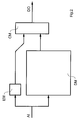
- FIG. 2 shows a possible diagram in greater detail of the device of FIG. 1 limited to the blocks affected by a writing operation.
- The address input AI of the device is connected to the address input of the memory means DM and the input of access to the memory means EM. The data outputs of the means DM and EM are connected to the error connection means inputs CM designed to combine the input signals. The output of the means CM is connected to the data output DO of the device.
- Depending on the type of error data contained in the memory means EM said means CM said means CM can consist of simple switches, means designed to identify and correct on the basis of the error data at the input, any errors in the user data, or in means designed to correct on the basis of the error data at the input specific errors occurring in the previous writing of the user data.
- Naturally the means CM must provide said operations only if error data associated with the address concerned are found in the memory means EM. This can be achieved e.g. by having the means EM generate a control signal indicating to the means CM the presence or not of the error data or, if error data is missing, having the combination of the input data with the means CM give as a result the unchanged user data. A mathematical example could be: the sum of "zero" with any number gives the same number.
- Four different possible detailed block diagrams of the device of FIG. 1 limited to the blocks affected by the writing operation are discussed below.
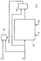
- With reference to FIG. 3 the first diagram represents the first memory means DM and the second memory means EM. Both are connected to the address input AI and the data input DI and furthermore the former exhibit a read/write control input R/W and the latter a writing enablement signal W-EN. The data input DI and the output of the means DM are connected to the inputs of the check means VM which are designed to generate in the writing phase a check signal corresponding to the comparison between the data at their input. Said check signal is sent to the input W-EN of the means EM.
- With this architecture the writing of the error data in the means EM takes place only if an error has occurred in writing the user data in the memory means DM. In the example of FIG. 3 the user data are memorised in the means EM after the finding of an error. Alternatively the user data can be memorised simultaneously in the means DM and EM and if no error is found the error data are erased from the means EM. The check signal is however to be sent to an erasure control input, not shown in FIG. 3, of the means EM.
- With reference to FIG. 4 the second diagram is the same as the former except that the data input DI is connected to the means EM not directly but through a first coder COD1. Said coder is capable of generating error data in such a manner that they correspond to the coding of the user data by means of an algorithm capable of identifying and correcting a predetermined number of errors.
- For a good discussion of said code and algorithm types reference can be had to the book by Jiri Adamek, "FOUNDATIONS OF CODING", John Wiley & Sons, 1991.
- Even for this diagram the same remarks made for the diagram of FIG. 3 apply . Furthermore the check signal can also be sent to an operational enablement input, not shown in FIG. 4, of the coder COD1. In this manner generation of the error data takes place only in case of a writing error.
- With reference to FIG. 5 the third diagram is identical to the second except that one of the inputs of the check means VM is connected to the output of the coder COD1 instead of to the data input DI. In this case generation of the error data takes place independently of any writing errors. The check means will comprise a more complex circuitry than that necessary in the above diagrams and indeed they must be so in order to identify the presence of data errors at the output of the means DM by using an algorithm corresponding to that used in the coder COD1.
- With reference to FIG. 6 the fourth diagram is a bit different from those discussed above. It represents the first memory means DM and the second memory means EM. Both are connected to the address input AI while only the former are connected to the data input DI and in addition the former exhibit an input R/W for read/write control and the latter a writing enablement signal W-EN and a data input. The data input DI and the output of the means DM are connected to the inputs of check means VM which are designed to generate in the writing phase a check signal corresponding to the comparison between the data at their input. More specifically the check signal consists in this case of a difference signal, which is sent to a second coder COD2, and an outcome signal which is sent to a writing logic WL. The output of the coder COD2 is sent to the data input of the means EM while the output of the writing logic WL is sent to the input W-EN of the means EM.
- The difference signal corresponds to the difference between the digital data making up the signals supplied to the inputs of the means VM. The outcome signal corresponds to the outcome of the comparison identity/non-identity between said digital data. The coder COD2 is then suitable to generate the error data in such a manner that they correspond to the coding of said difference.
- As mentioned above, the present invention finds advantageous employment for multilevel memories. In this case the memory means EM can be the multilevel type like the means DM or they can be the two-level type to ensure greater reliability.
- Further advantages are achieved if the first and second memory means consist of two semiconductor memory cell matrices and specifically the EEPROM or flash EPROM type.
- It is natural that even the memory means EM are subject to errors which can exist right from production or can appear during normal operation. In many cases said errors can be accepted given the small size of said means and hence the limited effect on productivity or on failures during operation. If this is not acceptable for any reason it can be thought to provide redundancy for memory means EM or apply thereto known error correction means or error correction means in accordance with the present invention.
- To be able to use such a type of memory device it is necessary to use reading, writing and erasure methods specifically adapted thereto.
- The method in accordance with the present invention for reading user data corrected by a memory device of the type comprising first memory means DM for containing user data designed to be accessed by means of address and second memory means EM for containing error data concerning the user data and designed to be accessed by means of content comprises the following phases:
- a) send to said device a reading address corresponding to the user data to be read,
- b) access by means of the reading address to user data addressed in the memory means DM,
- c) access by means of the content of the reading address to possible error data in the memory means EM, and
- d) combine the addressed user data and any error data to obtain the corrected user data.
- If there are no error data corresponding to said reading address the corrected data correspond to the addressed data and phase d) has no effect.
- One method in accordance with the present invention for writing corrected user data in a memory device of the type comprising first memory means DM for containing user data designed to be accessed by means of address and second memory means EM for containing error data concerning the user data designed to be accessed by means of content comprises the following phases:
- a) send to said device a writing address,
- b) send to said device user data to be memorised,
- c) write the user data to be memorised in the memory means DM in a position corresponding to the writing address,
- d) access by means of the writing address to user data addressed in the memory means DM,
- e) check the identity of the user data to be memorised and of the addressed user data and in case of failure of said check:
- f) generate error data capable of correcting errors in the addressed user data, and
- g) write the error data generated in the memory means EM and associate them with the writing address for access.
- An advantageous choice for its simplicity, the error data generated correspond to the user data to be memorised, hence phase f) has no effect.
- It may be important, in particular in the case of intermittent errors, to be able to reuse the memory cells of the means EM when they are no longer used for memorising error data associated with a certain address of the means DM. This occurs when the cells of the means DM corresponding to said certain address have first originated writing errors and subsequently resumed correct operation.
- The solution to this problem may be that, if the identity check does not fail, any error data associated with the writing address are erased from the means EM. Erasure will thus take place really only in the case or rewriting of cells which had previously originated writing errors.
- This erasure could take place, in a quite simple manner, e.g. by marking the error data as "erased" instead of erasing them physically.
- A second writing method in accordance with the present invention and an alternative to that discussed above but identical thereto in its essential part could be used if it is preferred to parallelise the operations of writing the user data in the means DM and of error data in the means EM.
- This comprises the following phases:
- a) send to said device a writing address,
- b) send to said device user data to be memorised,
- c) write the user data to be memorised in the means DM in a position corresponding to the writing address,
- d) access by means of the writing address to user data addressed in the means DM,
- e) generate error data capable of correcting errors in the addressed user data,
- f) write the error data in the means EM and associate them with the writing address for access,
- g) check the identity of the user data to be memorised and of the addressed user data, and
- h) if the check is successful, erase from the means EM the error data associated with the writing address.
- The two writing methods discussed refer to generic user data. As mentioned above, taking the term "write" in a broad sense, said methods can also be termed erasure methods when the erasure operation is thought of as the writing of a predetermined datum which is the same for all the cells or words.
- Based on this consideration said methods could be used also to overcome the problem of 'bit depletion' during erasure of the flash EPROM memories. Indeed, if after a normal total erasure of a device or of a sector of such a memory it is seen that few cells, for any reason, are not erased (i.e. do not contain the desired data) instead of continuing the total erasure of the memory, by applying the present methods error data are generated and written in the means EM. In this manner the possible erasure of the other cells is prevented.
- Often however the erasure operation refers to the mere marking of the 'erased' cell.
- The method in accordance with the present invention of erasing (in the most common sense of the term) user data in a memory device of the type comprising first memory means DM for containing user data designed to be accessed by means of address and second memory means EM for containing error data concerning the user data designed to be accessed by means of content comprises the following phases:
- a) send to said device an erasure address,
- b) erase from the means DM user data in a position corresponding to the erasure address, and
- c) erase from the means EM any associated error data for access to the erasure address.
- Not all the devices in general have the erasure function and more often the memory cells are rewritten. In this case the procedure for reuse of the cells of the memory EM is discussed above.
Claims (16)
- Memory device and specifically the multilevel type with error check and correction function and having a data input (DI), a data output (DO) and an address input (AI) and of the type comprising:a) first memory means (DM) designed to be accessed by means of address for containing user data,b) second memory means (EM) for containing error data concerning said user data,c) a control logic (CL) designed to receive in the writing phase from said address input (AI) and said data input (DI) a writing address and user data respectively to generate error data and to write said data in said first (DM) and second (EM) means respectively and designed to receive in the reading phase from said address input (AI) a reading address and to extract corresponding user data and error data and to combine them for correction of any errors and to supply them to said data output (DO) and characterised in that said second means (EM) are the type designed to be accessed by means of content and said content for access corresponding to addresses of said first means (DM).
- Device in accordance with claim 1 in which said control logic (CL) comprises check means (VM) designed to generate in the writing phase a check signal corresponding to the comparison between said user data and the data written in said first means (DM) and in which said check signal enables the writing of said second means (EM) if an error occurs in writing said user data in said first means (DM).
- Device in accordance with claim 2 in which said check signal enables furthermore the generation of said error data in the writing phase.
- Device in accordance with claim 1 in which said control logic (CL) comprises check means (VM) designed to generate in the writing phase a check signal corresponding to the comparison between said user data and the data written in said first means (DM) and in which said check signal enables erasure from said second means (EM) of said error data if no error occurs in the writing of said user data in said first means (DM).
- Device in accordance with claim 1 in which said error data correspond to said user data.
- Device in accordance with claim 1 comprising furthermore a coder (COD1) designed to generate said error data in such a manner that they correspond to the coding of said user data by means of an algorithm capable of identifying and correcting a predetermined number of errors.
- Device in accordance with claim 1 comprising furthermore a coder (COD2) designed to generate said error data in such a manner that they correspond to the coding of the difference between said user data and the data written in said first means (DM).
- Device in accordance with claim 1 in which said first means (DM) are the multilevel type and said second means (EM) are the two-level type.
- Device in accordance with claim 1 in which said first (DM) and second (EM) means consist of two semiconductor memory cell matrices and specifically the EEPROM or flash EPROM type.
- Method of reading corrected user data from a memory device of the type comprising first memory means (DM) for containing user data designed to be accessed by means of address and second memory means (EM) for containing error data concerning said user data designed to be accessed by means of content and comprising the following phases.a) send to said device a reading address corresponding to the user data to be read,b) access by means of said reading address to user data addressed in said memory means (DM),c) access by means of the content of said reading address to any error data in said memory means (EM), andd) combine said addressed user data and any error data to obtain said corrected user data.
- Reading method in accordance with claim 10 in which if there are no error data corresponding to said reading address said corrected data correspond to said addressed data and said phase d) has no effect.
- Method for writing corrected user data in a memory device of the type comprising first memory means (DM) for containing user data designed to be accessed by means of address and second memory means (EM) for containing error data concerning said user data designed to be accessed by means of content and comprising the following phases:a) send to said device a writing address,b) send to said device user data to be memorised,c) write the user data to be memorised in said memory means (DM) in a position corresponding to said writing address,d) access by means of said writing address to user data addressed in said first memory means (DM),e) check the identity of said user data to be memorised and of said addressed user data and in case of failure of said check:f) generate error data capable of correcting errors in the addressed user data, andg) write said error data generated in said memory means (EM) and associate them for access to said writing address.
- Writing method in accordance with claim 12 in which said generated error data correspond to said user data to be memorised and said phase f) has no effect.
- Writing method in accordance with claim 12 in which in case of non-failure of said check there are erased from said second means (EM) any error data associated with said writing address.
- Method of writing corrected user data in a memory device of the type comprising first memory means (DM) for containing user data designed to be accessed by means of address and second memory means (EM) for containing error data concerning said user data and comprising the following phases.a) send to said device a writing address,b) send to said device user data to be memorised,c) write said user data to be memorised in said first means (DM) in a position corresponding to said writing address,d) access by means of said writing address to user data addressed in said first means (DM),e) generate error data capable of correcting errors in said addressed user data,f) write said error data in said second means (EM) and associate them with said writing address for access,g) check the identity of said user data to be memorised and of said addressed user data, andh) if the check is successful erase from said second means (EM) the error data associated with said writing address.
- Method of erasing user data in a memory device of the type comprising first memory means (DM) for containing user data designed to be accessed by means of address and second memory means (EM) for containing error data concerning said user data designed to be accessed by means of content and comprising the following phases:a) send to said device an erasure address,b) erase from said first means (DM) user data in a position corresponding to the erasure address, andc) erase from said second means (EM) any associated error data for access to said erasure address.
Priority Applications (4)
| Application Number | Priority Date | Filing Date | Title |
|---|---|---|---|
| EP94830471A EP0704854B1 (en) | 1994-09-30 | 1994-09-30 | Memory device having error detection and correction function, and methods for writing and erasing the memory device |
| DE69421925T DE69421925T2 (en) | 1994-09-30 | 1994-09-30 | Storage device with error detection and correction and method for writing and erasing the storage device |
| JP25404695A JP3704184B2 (en) | 1994-09-30 | 1995-09-29 | Memory device, method of reading corrected user data from memory device, method of writing corrected user data to memory device, and method of erasing user data of memory device |
| US08/538,161 US5761222A (en) | 1994-09-30 | 1995-10-02 | Memory device having error detection and correction function, and methods for reading, writing and erasing the memory device |
Applications Claiming Priority (1)
| Application Number | Priority Date | Filing Date | Title |
|---|---|---|---|
| EP94830471A EP0704854B1 (en) | 1994-09-30 | 1994-09-30 | Memory device having error detection and correction function, and methods for writing and erasing the memory device |
Publications (2)
| Publication Number | Publication Date |
|---|---|
| EP0704854A1 true EP0704854A1 (en) | 1996-04-03 |
| EP0704854B1 EP0704854B1 (en) | 1999-12-01 |
Family
ID=8218548
Family Applications (1)
| Application Number | Title | Priority Date | Filing Date |
|---|---|---|---|
| EP94830471A Expired - Lifetime EP0704854B1 (en) | 1994-09-30 | 1994-09-30 | Memory device having error detection and correction function, and methods for writing and erasing the memory device |
Country Status (4)
| Country | Link |
|---|---|
| US (1) | US5761222A (en) |
| EP (1) | EP0704854B1 (en) |
| JP (1) | JP3704184B2 (en) |
| DE (1) | DE69421925T2 (en) |
Cited By (6)
| Publication number | Priority date | Publication date | Assignee | Title |
|---|---|---|---|---|
| US6647151B1 (en) * | 1999-08-18 | 2003-11-11 | Hewlett-Packard Development Company, L.P. | Coalescence of device independent bitmaps for artifact avoidance |
| EP2026355A3 (en) * | 2007-08-14 | 2009-04-01 | Dell Products, L.P. | System and method for implementing a memory defect map |
| US7694195B2 (en) | 2007-08-14 | 2010-04-06 | Dell Products L.P. | System and method for using a memory mapping function to map memory defects |
| US7945815B2 (en) | 2007-08-14 | 2011-05-17 | Dell Products L.P. | System and method for managing memory errors in an information handling system |
| US7949913B2 (en) | 2007-08-14 | 2011-05-24 | Dell Products L.P. | Method for creating a memory defect map and optimizing performance using the memory defect map |
| US8014197B2 (en) | 2005-08-02 | 2011-09-06 | Sandisk Technologies Inc. | System and method for programming cells in non-volatile integrated memory devices |
Families Citing this family (50)
| Publication number | Priority date | Publication date | Assignee | Title |
|---|---|---|---|---|
| US6857099B1 (en) * | 1996-09-18 | 2005-02-15 | Nippon Steel Corporation | Multilevel semiconductor memory, write/read method thereto/therefrom and storage medium storing write/read program |
| US5859858A (en) * | 1996-10-25 | 1999-01-12 | Intel Corporation | Method and apparatus for correcting a multilevel cell memory by using error locating codes |
| US6212654B1 (en) | 1997-07-22 | 2001-04-03 | Lucent Technologies Inc. | Coded modulation for digital storage in analog memory devices |
| KR100333720B1 (en) * | 1998-06-30 | 2002-06-20 | 박종섭 | A redundancy circuit in ferroelectric memory device |
| AU1634600A (en) * | 1998-12-30 | 2000-07-24 | Intel Corporation | Memory array organization |
| US6532556B1 (en) | 2000-01-27 | 2003-03-11 | Multi Level Memory Technology | Data management for multi-bit-per-cell memories |
| US6466476B1 (en) | 2001-01-18 | 2002-10-15 | Multi Level Memory Technology | Data coding for multi-bit-per-cell memories having variable numbers of bits per memory cell |
| US6700827B2 (en) | 2001-02-08 | 2004-03-02 | Integrated Device Technology, Inc. | Cam circuit with error correction |
| US6987684B1 (en) | 2003-07-15 | 2006-01-17 | Integrated Device Technology, Inc. | Content addressable memory (CAM) devices having multi-block error detection logic and entry selective error correction logic therein |
| US7193876B1 (en) | 2003-07-15 | 2007-03-20 | Kee Park | Content addressable memory (CAM) arrays having memory cells therein with different susceptibilities to soft errors |
| US6870749B1 (en) | 2003-07-15 | 2005-03-22 | Integrated Device Technology, Inc. | Content addressable memory (CAM) devices with dual-function check bit cells that support column redundancy and check bit cells with reduced susceptibility to soft errors |
| US7304875B1 (en) | 2003-12-17 | 2007-12-04 | Integrated Device Technology. Inc. | Content addressable memory (CAM) devices that support background BIST and BISR operations and methods of operating same |
| US6888758B1 (en) * | 2004-01-21 | 2005-05-03 | Sandisk Corporation | Programming non-volatile memory |
| US7372730B2 (en) * | 2004-01-26 | 2008-05-13 | Sandisk Corporation | Method of reading NAND memory to compensate for coupling between storage elements |
| US7068539B2 (en) * | 2004-01-27 | 2006-06-27 | Sandisk Corporation | Charge packet metering for coarse/fine programming of non-volatile memory |
| US7139198B2 (en) * | 2004-01-27 | 2006-11-21 | Sandisk Corporation | Efficient verification for coarse/fine programming of non-volatile memory |
| US7002843B2 (en) * | 2004-01-27 | 2006-02-21 | Sandisk Corporation | Variable current sinking for coarse/fine programming of non-volatile memory |
| US7023733B2 (en) * | 2004-05-05 | 2006-04-04 | Sandisk Corporation | Boosting to control programming of non-volatile memory |
| US7020026B2 (en) * | 2004-05-05 | 2006-03-28 | Sandisk Corporation | Bitline governed approach for program control of non-volatile memory |
| US7099221B2 (en) | 2004-05-06 | 2006-08-29 | Micron Technology, Inc. | Memory controller method and system compensating for memory cell data losses |
| US20060010339A1 (en) * | 2004-06-24 | 2006-01-12 | Klein Dean A | Memory system and method having selective ECC during low power refresh |
| US7340668B2 (en) * | 2004-06-25 | 2008-03-04 | Micron Technology, Inc. | Low power cost-effective ECC memory system and method |
| US7116602B2 (en) | 2004-07-15 | 2006-10-03 | Micron Technology, Inc. | Method and system for controlling refresh to avoid memory cell data losses |
| US6965537B1 (en) * | 2004-08-31 | 2005-11-15 | Micron Technology, Inc. | Memory system and method using ECC to achieve low power refresh |
| US7092290B2 (en) * | 2004-11-16 | 2006-08-15 | Sandisk Corporation | High speed programming system with reduced over programming |
| US7173859B2 (en) * | 2004-11-16 | 2007-02-06 | Sandisk Corporation | Faster programming of higher level states in multi-level cell flash memory |
| US7339834B2 (en) * | 2005-06-03 | 2008-03-04 | Sandisk Corporation | Starting program voltage shift with cycling of non-volatile memory |
| US7286406B2 (en) * | 2005-10-14 | 2007-10-23 | Sandisk Corporation | Method for controlled programming of non-volatile memory exhibiting bit line coupling |
| US7206235B1 (en) | 2005-10-14 | 2007-04-17 | Sandisk Corporation | Apparatus for controlled programming of non-volatile memory exhibiting bit line coupling |
| EP2315212A1 (en) | 2006-04-12 | 2011-04-27 | Sandisk Corporation | Reducing the impact of program disturb during read |
| US7486561B2 (en) * | 2006-06-22 | 2009-02-03 | Sandisk Corporation | Method for non-real time reprogramming of non-volatile memory to achieve tighter distribution of threshold voltages |
| US7489549B2 (en) * | 2006-06-22 | 2009-02-10 | Sandisk Corporation | System for non-real time reprogramming of non-volatile memory to achieve tighter distribution of threshold voltages |
| US7474561B2 (en) * | 2006-10-10 | 2009-01-06 | Sandisk Corporation | Variable program voltage increment values in non-volatile memory program operations |
| US7450426B2 (en) * | 2006-10-10 | 2008-11-11 | Sandisk Corporation | Systems utilizing variable program voltage increment values in non-volatile memory program operations |
| US7894289B2 (en) | 2006-10-11 | 2011-02-22 | Micron Technology, Inc. | Memory system and method using partial ECC to achieve low power refresh and fast access to data |
| US7900120B2 (en) | 2006-10-18 | 2011-03-01 | Micron Technology, Inc. | Memory system and method using ECC with flag bit to identify modified data |
| US7570520B2 (en) * | 2006-12-27 | 2009-08-04 | Sandisk Corporation | Non-volatile storage system with initial programming voltage based on trial |
| US7551482B2 (en) * | 2006-12-27 | 2009-06-23 | Sandisk Corporation | Method for programming with initial programming voltage based on trial |
| US8365044B2 (en) * | 2007-04-23 | 2013-01-29 | Agere Systems Inc. | Memory device with error correction based on automatic logic inversion |
| US7508715B2 (en) * | 2007-07-03 | 2009-03-24 | Sandisk Corporation | Coarse/fine program verification in non-volatile memory using different reference levels for improved sensing |
| US7599224B2 (en) * | 2007-07-03 | 2009-10-06 | Sandisk Corporation | Systems for coarse/fine program verification in non-volatile memory using different reference levels for improved sensing |
| US8625320B1 (en) | 2010-08-31 | 2014-01-07 | Netlogic Microsystems, Inc. | Quaternary content addressable memory cell having one transistor pull-down stack |
| US8462532B1 (en) | 2010-08-31 | 2013-06-11 | Netlogic Microsystems, Inc. | Fast quaternary content addressable memory cell |
| US8582338B1 (en) | 2010-08-31 | 2013-11-12 | Netlogic Microsystems, Inc. | Ternary content addressable memory cell having single transistor pull-down stack |
| US8553441B1 (en) | 2010-08-31 | 2013-10-08 | Netlogic Microsystems, Inc. | Ternary content addressable memory cell having two transistor pull-down stack |
| US8773880B2 (en) | 2011-06-23 | 2014-07-08 | Netlogic Microsystems, Inc. | Content addressable memory array having virtual ground nodes |
| US8837188B1 (en) | 2011-06-23 | 2014-09-16 | Netlogic Microsystems, Inc. | Content addressable memory row having virtual ground and charge sharing |
| US8724408B2 (en) | 2011-11-29 | 2014-05-13 | Kingtiger Technology (Canada) Inc. | Systems and methods for testing and assembling memory modules |
| US9117552B2 (en) | 2012-08-28 | 2015-08-25 | Kingtiger Technology(Canada), Inc. | Systems and methods for testing memory |
| US10387251B2 (en) * | 2017-07-17 | 2019-08-20 | Cisco Technology, Inc. | Error detection and correction in a content-addressable memory using single-bit position lookup operations |
Citations (5)
| Publication number | Priority date | Publication date | Assignee | Title |
|---|---|---|---|---|
| US4058851A (en) * | 1976-10-18 | 1977-11-15 | Sperry Rand Corporation | Conditional bypass of error correction for dual memory access time selection |
| US4249253A (en) * | 1977-12-23 | 1981-02-03 | Honeywell Information Systems Italia | Memory with selective intervention error checking and correcting device |
| EP0042966A1 (en) * | 1980-06-30 | 1982-01-06 | International Business Machines Corporation | Digital data storage error detecting and correcting system and method |
| US4654847A (en) * | 1984-12-28 | 1987-03-31 | International Business Machines | Apparatus for automatically correcting erroneous data and for storing the corrected data in a common pool alternate memory array |
| EP0485976A2 (en) * | 1990-11-13 | 1992-05-20 | Kabushiki Kaisha Toshiba | Fault analysis apparatus for memories having redundancy circuits |
-
1994
- 1994-09-30 DE DE69421925T patent/DE69421925T2/en not_active Expired - Fee Related
- 1994-09-30 EP EP94830471A patent/EP0704854B1/en not_active Expired - Lifetime
-
1995
- 1995-09-29 JP JP25404695A patent/JP3704184B2/en not_active Expired - Fee Related
- 1995-10-02 US US08/538,161 patent/US5761222A/en not_active Expired - Lifetime
Patent Citations (5)
| Publication number | Priority date | Publication date | Assignee | Title |
|---|---|---|---|---|
| US4058851A (en) * | 1976-10-18 | 1977-11-15 | Sperry Rand Corporation | Conditional bypass of error correction for dual memory access time selection |
| US4249253A (en) * | 1977-12-23 | 1981-02-03 | Honeywell Information Systems Italia | Memory with selective intervention error checking and correcting device |
| EP0042966A1 (en) * | 1980-06-30 | 1982-01-06 | International Business Machines Corporation | Digital data storage error detecting and correcting system and method |
| US4654847A (en) * | 1984-12-28 | 1987-03-31 | International Business Machines | Apparatus for automatically correcting erroneous data and for storing the corrected data in a common pool alternate memory array |
| EP0485976A2 (en) * | 1990-11-13 | 1992-05-20 | Kabushiki Kaisha Toshiba | Fault analysis apparatus for memories having redundancy circuits |
Cited By (7)
| Publication number | Priority date | Publication date | Assignee | Title |
|---|---|---|---|---|
| US6647151B1 (en) * | 1999-08-18 | 2003-11-11 | Hewlett-Packard Development Company, L.P. | Coalescence of device independent bitmaps for artifact avoidance |
| US8014197B2 (en) | 2005-08-02 | 2011-09-06 | Sandisk Technologies Inc. | System and method for programming cells in non-volatile integrated memory devices |
| EP2026355A3 (en) * | 2007-08-14 | 2009-04-01 | Dell Products, L.P. | System and method for implementing a memory defect map |
| US7694195B2 (en) | 2007-08-14 | 2010-04-06 | Dell Products L.P. | System and method for using a memory mapping function to map memory defects |
| US7945815B2 (en) | 2007-08-14 | 2011-05-17 | Dell Products L.P. | System and method for managing memory errors in an information handling system |
| US7949913B2 (en) | 2007-08-14 | 2011-05-24 | Dell Products L.P. | Method for creating a memory defect map and optimizing performance using the memory defect map |
| US9373362B2 (en) | 2007-08-14 | 2016-06-21 | Dell Products L.P. | System and method for implementing a memory defect map |
Also Published As
| Publication number | Publication date |
|---|---|
| US5761222A (en) | 1998-06-02 |
| DE69421925T2 (en) | 2000-03-16 |
| JPH08123737A (en) | 1996-05-17 |
| JP3704184B2 (en) | 2005-10-05 |
| EP0704854B1 (en) | 1999-12-01 |
| DE69421925D1 (en) | 2000-01-05 |
Similar Documents
| Publication | Publication Date | Title |
|---|---|---|
| EP0704854B1 (en) | Memory device having error detection and correction function, and methods for writing and erasing the memory device | |
| US6178537B1 (en) | Method and apparatus for performing error correction on data read from a multistate memory | |
| US6839875B2 (en) | Method and apparatus for performing error correction on data read from a multistate memory | |
| US10459794B2 (en) | Memory systems having extended product lifetime and methods of operating the same | |
| US6549457B1 (en) | Using multiple status bits per cell for handling power failures during write operations | |
| US5247523A (en) | Code error correction apparatus | |
| JP3982639B2 (en) | Method for reading data from a memory having multi-level cells | |
| US6112314A (en) | Apparatus and method for detecting over-programming condition in multistate memory device | |
| US4612640A (en) | Error checking and correction circuitry for use with an electrically-programmable and electrically-erasable memory array | |
| JP2821278B2 (en) | Semiconductor integrated circuit | |
| US8015370B2 (en) | Memory control method and memory system | |
| US7178067B2 (en) | Secure EEPROM memory comprising an error correction circuit | |
| US5432802A (en) | Information processing device having electrically erasable programmable read only memory with error check and correction circuit | |
| JPH08235887A (en) | Electrically programmable memory and write method of data into memory | |
| CN102394101A (en) | Memory device with adaptive capacity | |
| US9390801B2 (en) | Secure memory which reduces degradation of data | |
| US7506199B2 (en) | Method and apparatus for recording and reproducing information | |
| EP0438050B1 (en) | Nonvolatile semiconductor memory system | |
| EP0428396B1 (en) | Bit error correcting circuit for a nonvolatile memory | |
| US6320791B1 (en) | Writing apparatus for a non-volatile semiconductor memory device | |
| JPH09180496A (en) | Semiconductor memory device | |
| EP1460542B1 (en) | Integrated memory system comprising at least a non-volatile memory and an automatic error corrector | |
| JPS6349860A (en) | Using system for e2prom | |
| JPH11203892A (en) | Semiconductor nonvolatile memory device | |
| US7663920B2 (en) | Memory system and data reading and generating method |
Legal Events
| Date | Code | Title | Description |
|---|---|---|---|
| PUAI | Public reference made under article 153(3) epc to a published international application that has entered the european phase |
Free format text: ORIGINAL CODE: 0009012 |
|
| AK | Designated contracting states |
Kind code of ref document: A1 Designated state(s): DE FR GB IT |
|
| K1C1 | Correction of patent application (title page) published |
Effective date: 19960403 |
|
| 17P | Request for examination filed |
Effective date: 19960925 |
|
| 17Q | First examination report despatched |
Effective date: 19980603 |
|
| RAP3 | Party data changed (applicant data changed or rights of an application transferred) |
Owner name: STMICROELECTRONICS S.R.L. |
|
| GRAG | Despatch of communication of intention to grant |
Free format text: ORIGINAL CODE: EPIDOS AGRA |
|
| GRAG | Despatch of communication of intention to grant |
Free format text: ORIGINAL CODE: EPIDOS AGRA |
|
| GRAH | Despatch of communication of intention to grant a patent |
Free format text: ORIGINAL CODE: EPIDOS IGRA |
|
| GRAH | Despatch of communication of intention to grant a patent |
Free format text: ORIGINAL CODE: EPIDOS IGRA |
|
| GRAA | (expected) grant |
Free format text: ORIGINAL CODE: 0009210 |
|
| ITF | It: translation for a ep patent filed |
Owner name: BOTTI & FERRARI S.R.L. |
|
| AK | Designated contracting states |
Kind code of ref document: B1 Designated state(s): DE FR GB IT |
|
| ET | Fr: translation filed | ||
| REF | Corresponds to: |
Ref document number: 69421925 Country of ref document: DE Date of ref document: 20000105 |
|
| PLBE | No opposition filed within time limit |
Free format text: ORIGINAL CODE: 0009261 |
|
| STAA | Information on the status of an ep patent application or granted ep patent |
Free format text: STATUS: NO OPPOSITION FILED WITHIN TIME LIMIT |
|
| 26N | No opposition filed | ||
| REG | Reference to a national code |
Ref country code: GB Ref legal event code: IF02 |
|
| PGFP | Annual fee paid to national office [announced via postgrant information from national office to epo] |
Ref country code: DE Payment date: 20030909 Year of fee payment: 10 |
|
| PG25 | Lapsed in a contracting state [announced via postgrant information from national office to epo] |
Ref country code: DE Free format text: LAPSE BECAUSE OF NON-PAYMENT OF DUE FEES Effective date: 20050401 |
|
| PG25 | Lapsed in a contracting state [announced via postgrant information from national office to epo] |
Ref country code: IT Free format text: LAPSE BECAUSE OF NON-PAYMENT OF DUE FEES;WARNING: LAPSES OF ITALIAN PATENTS WITH EFFECTIVE DATE BEFORE 2007 MAY HAVE OCCURRED AT ANY TIME BEFORE 2007. THE CORRECT EFFECTIVE DATE MAY BE DIFFERENT FROM THE ONE RECORDED. Effective date: 20050930 |
|
| PGFP | Annual fee paid to national office [announced via postgrant information from national office to epo] |
Ref country code: GB Payment date: 20060217 Year of fee payment: 12 |
|
| PGFP | Annual fee paid to national office [announced via postgrant information from national office to epo] |
Ref country code: FR Payment date: 20060227 Year of fee payment: 12 |
|
| GBPC | Gb: european patent ceased through non-payment of renewal fee |
Effective date: 20060930 |
|
| REG | Reference to a national code |
Ref country code: FR Ref legal event code: ST Effective date: 20070531 |
|
| PG25 | Lapsed in a contracting state [announced via postgrant information from national office to epo] |
Ref country code: GB Free format text: LAPSE BECAUSE OF NON-PAYMENT OF DUE FEES Effective date: 20060930 |
|
| PG25 | Lapsed in a contracting state [announced via postgrant information from national office to epo] |
Ref country code: FR Free format text: LAPSE BECAUSE OF NON-PAYMENT OF DUE FEES Effective date: 20061002 |