EP0717415B1 - Semiconductor memory device - Google Patents
Semiconductor memory device Download PDFInfo
- Publication number
- EP0717415B1 EP0717415B1 EP95118297A EP95118297A EP0717415B1 EP 0717415 B1 EP0717415 B1 EP 0717415B1 EP 95118297 A EP95118297 A EP 95118297A EP 95118297 A EP95118297 A EP 95118297A EP 0717415 B1 EP0717415 B1 EP 0717415B1
- Authority
- EP
- European Patent Office
- Prior art keywords
- circuit
- transistors
- vpp
- circuits
- gates
- Prior art date
- Legal status (The legal status is an assumption and is not a legal conclusion. Google has not performed a legal analysis and makes no representation as to the accuracy of the status listed.)
- Expired - Lifetime
Links
Images


Classifications
-
- G—PHYSICS
- G11—INFORMATION STORAGE
- G11C—STATIC STORES
- G11C11/00—Digital stores characterised by the use of particular electric or magnetic storage elements; Storage elements therefor
- G11C11/21—Digital stores characterised by the use of particular electric or magnetic storage elements; Storage elements therefor using electric elements
- G11C11/34—Digital stores characterised by the use of particular electric or magnetic storage elements; Storage elements therefor using electric elements using semiconductor devices
- G11C11/40—Digital stores characterised by the use of particular electric or magnetic storage elements; Storage elements therefor using electric elements using semiconductor devices using transistors
- G11C11/401—Digital stores characterised by the use of particular electric or magnetic storage elements; Storage elements therefor using electric elements using semiconductor devices using transistors forming cells needing refreshing or charge regeneration, i.e. dynamic cells
- G11C11/4063—Auxiliary circuits, e.g. for addressing, decoding, driving, writing, sensing or timing
- G11C11/407—Auxiliary circuits, e.g. for addressing, decoding, driving, writing, sensing or timing for memory cells of the field-effect type
- G11C11/408—Address circuits
- G11C11/4087—Address decoders, e.g. bit - or word line decoders; Multiple line decoders
-
- G—PHYSICS
- G11—INFORMATION STORAGE
- G11C—STATIC STORES
- G11C11/00—Digital stores characterised by the use of particular electric or magnetic storage elements; Storage elements therefor
- G11C11/21—Digital stores characterised by the use of particular electric or magnetic storage elements; Storage elements therefor using electric elements
- G11C11/34—Digital stores characterised by the use of particular electric or magnetic storage elements; Storage elements therefor using electric elements using semiconductor devices
- G11C11/40—Digital stores characterised by the use of particular electric or magnetic storage elements; Storage elements therefor using electric elements using semiconductor devices using transistors
- G11C11/401—Digital stores characterised by the use of particular electric or magnetic storage elements; Storage elements therefor using electric elements using semiconductor devices using transistors forming cells needing refreshing or charge regeneration, i.e. dynamic cells
- G11C11/4063—Auxiliary circuits, e.g. for addressing, decoding, driving, writing, sensing or timing
- G11C11/407—Auxiliary circuits, e.g. for addressing, decoding, driving, writing, sensing or timing for memory cells of the field-effect type
- G11C11/408—Address circuits
- G11C11/4085—Word line control circuits, e.g. word line drivers, - boosters, - pull-up, - pull-down, - precharge
-
- G—PHYSICS
- G11—INFORMATION STORAGE
- G11C—STATIC STORES
- G11C11/00—Digital stores characterised by the use of particular electric or magnetic storage elements; Storage elements therefor
- G11C11/21—Digital stores characterised by the use of particular electric or magnetic storage elements; Storage elements therefor using electric elements
- G11C11/34—Digital stores characterised by the use of particular electric or magnetic storage elements; Storage elements therefor using electric elements using semiconductor devices
- G11C11/40—Digital stores characterised by the use of particular electric or magnetic storage elements; Storage elements therefor using electric elements using semiconductor devices using transistors
- G11C11/401—Digital stores characterised by the use of particular electric or magnetic storage elements; Storage elements therefor using electric elements using semiconductor devices using transistors forming cells needing refreshing or charge regeneration, i.e. dynamic cells
- G11C11/4063—Auxiliary circuits, e.g. for addressing, decoding, driving, writing, sensing or timing
- G11C11/407—Auxiliary circuits, e.g. for addressing, decoding, driving, writing, sensing or timing for memory cells of the field-effect type
- G11C11/409—Read-write [R-W] circuits
- G11C11/4091—Sense or sense/refresh amplifiers, or associated sense circuitry, e.g. for coupled bit-line precharging, equalising or isolating
-
- G—PHYSICS
- G11—INFORMATION STORAGE
- G11C—STATIC STORES
- G11C5/00—Details of stores covered by group G11C11/00
- G11C5/14—Power supply arrangements, e.g. power down, chip selection or deselection, layout of wirings or power grids, or multiple supply levels
- G11C5/145—Applications of charge pumps; Boosted voltage circuits; Clamp circuits therefor
Definitions
- the conventional DRAM has utilized boot-strap-type word line driving circuits, which use N channel MOS transistors as word line drivers in word line driving circuits.
- This technology is disclosed in IEEE ISSCC DIGEST OF TECHNICAL PAPERS PP12-13 February 16, 1977. Meanwhile, reduction of power supply voltage and advancement of micro lithography technology have realized an arrangement of P channel type MOS transistors as word line drivers on every word line. Therefore a newly developed 64M bit DRAM has word line driving circuits each of which has a P channel MOS transistor, and a booster circuit to generate a word line driving voltage, which cause no threshold voltage drop of the word line driving voltage across the P channel MOS transistor.
- a booster circuit is formed in a chip, a capacitor which is connected to the output of the booster circuit occupies a very large area in order to stabilize the output potential. Accordingly, a conventional DRAM with built-in booster circuit has a problem of chip area increase.
- US-A-5,267,214 and JP06-203600 disclose dynamic random access memory arrangements including a sense amplifier band shared between two different memory blocks. In this memory, only sense amplifiers related to a selected memory block are activated.
- the memory comprises a circuit for boosting a control signal voltage to a switching unit for connecting the selected memory block to the sense amplifiers up to a level higher than a power supply voltage V cc during the activation of the sense amplifiers, and a circuit for separating a memory block paired with the selected memory block from the activated sense amplifiers during the sensing operation.
- the memory further comprises a circuit for generating a control signal of the power supply voltage V cc and connecting all the memory blocks to the corresponding sense amplifiers in a stand-by state so as to reduce power consumption arising from the charge and discharge of the parasitic capacitance of the separating circuit.
- the present invention relates to a semiconductor memory, more particularly, to a DRAM (dynamic type random access memory) of a shared sense amplifier structure, which includes a booster circuit for generating a stationary boosted potential as a word line driving potential.
- DRAM dynamic type random access memory
- a semiconductor memory device comprising: a booster circuit generating a boosted potential; a first memory cell array including first pairs of bit lines; a second memory cell array including second pairs of bit lines; a sense amplifier circuit; a first transmission gate circuit having pairs of transistors for connecting the first pairs of bit lines to the sense amplifier circuit; a second transmission gate circuit having pairs of transistors for connecting the second pairs of bit lines to the sense amplifier circuit; a first equalizing circuit having transistors equalizing the first pairs of bit lines; a second equalizing circuit having transistors equalizing the second pairs of bit lines; and a control circuit applying the boosted voltage respectively to gates of the transistors in the first and the second transmission gate circuits and gates of the transistors in the first and the second equalizing circuits when none of memory cells in the first and the second memory cell arrays is selected.
- the boosted potential is applied on the gates of the transistors in the first and the second transmission gate circuits when none of the memory cells of the first and the second memory cell arrays is selected. That is, at this moment these transistors work as capacitive elements to be connected to the output of the booster circuit. Accordingly, the capacitance to be connected to the output of the booster circuit can be reduced by an amount corresponding to the parasitic capacitance of these transistors.
- the half work as capacitive elements and the capacitance to be connected to the booster circuit can be reduced by an amount corresponding to their parasitic capacitance.
- the transistors of the transmission gates and the like which have conventionally been connected to the ground potential in a nonselection time, are used as the capacitor for the booster circuit by which the area of the capacitive elements can be reduced by an amount corresponding to the parasitic capacitance.
- Fig. 1 shows essential parts of the present invention which are constituted by a first memory cell array MCA1, a second memory cell array MCA2, a pair of left bit lines BLL and /BLL, a pair of right bit lines BLR and /BLR, a sense amplifier S/A and the like.
- the embodiment includes a left bit line pair equalizing circuit constituted by N-channel MOS transistors Q1, Q2 and Q3, a left transmission gate constituted by N-channel MOS transistors Q4 and Q5, a right bit line pair equalizing circuit constituted by N-channel MOS transistors Q6, Q7 and Q8 and a right transmission gate circuit constituted by N-channel MOS transistors Q9 and Q10.
- a plurality of dynamic type memory cells are arranged in a matrix in each of the memory cell arrays MCA1 and MCA2.
- the memory cells belonging to the same column are connected by the same pair of bit lines and the memory cells belonging to the same row are connected by the same word line.
- the left bit line pair equalizing circuit is controlled by a signal ⁇ E1.
- ⁇ E1 is at a boosted potential Vpp (for example, 4.3V in comparison with ground potential )
- VBL for example, 1.5V which is about a half of potential of VDD that is an inner power source potential
- ⁇ E1 When ⁇ E1 is at a ground potential Vss (0V) all the MOS transistors in the circuit are made nonconductive.
- the right bit line pair equalizing circuit is controlled by a signal ⁇ E2.
- VBL When ⁇ E2 is at the boosted potential Vpp, VBL is supplied to the right bit line pair BLR and /BLR and the both are shortcircuited.
- ⁇ E2 When ⁇ E2 is at the ground potential Vss, all the MOS transistors in the circuit are made nonconductive.
- the left transmission gate circuit is controlled by a signal ⁇ T2.
- ⁇ T2 When ⁇ T2 is at the boosted potential Vpp, the left bit line pair BLL and/BLL is connected to the sense amplifier S/A .
- ⁇ T2 When ⁇ T2 is at the ground potential Vss, the left bit line pair BLL and /BLL and the sense amplifier S/A are disconnected from each other.
- the right transmission gate circuit is controlled by a signal ⁇ T1.
- ⁇ T1 When ⁇ T1 is at the boosted potential Vpp, the right bit line pair BLR and /BLR are connected to the sense amplifier S/A.
- ⁇ T1 is at the ground potential Vss, the right bit line pair BLR and/BLR and the sense amplifier S/A are disconnected from each other.
- ⁇ E1 is changed from Vpp to Vss
- ⁇ T2 is maintained as Vpp
- ⁇ T1 is changed from Vpp to Vss
- ⁇ E2 is maintained as Vpp by which the sense amplifier S/A and the second memory cell array MCA2 are disconnected from each other and the equalizing operation of the left equalizing circuit is released.
- ⁇ E1 is maintained as Vpp
- ⁇ T2 is changed from Vpp to Vss
- ⁇ T1 is maintained as Vpp
- ⁇ T2 is changed from Vpp to Vss by which the sense amplifier S/A and the first memory cell array MCA1 are disconnected from each other and the equalizing operation of the right equalizing circuit is released.
- the area of the capacitive elements can be reduced by the amount of their parasitic capacitance.
- Fig. 2 shows essential parts of the present invention and the details of a control system.
- the control system is constituted by a booster circuit VPPGEN generating the boosted potential Vpp from an inner power source potential VDD, a capacitor DC (hereinafter, de-coupling capacitor), a circuit 221 for selecting and driving MCA1 which includes a first level shift circuit 201 and a first drive circuit 211, a circuit 222 for selecting and driving MCA2 which includes a second level shift circuit 202 and a second drive circuit 212, a row decode circuit 23, a word line driving circuit 24 and the like.
- VPPGEN generating the boosted potential Vpp from an inner power source potential VDD
- a capacitor DC hereinafter, de-coupling capacitor
- a circuit 221 for selecting and driving MCA1 which includes a first level shift circuit 201 and a first drive circuit 211
- a circuit 222 for selecting and driving MCA2 which includes a second level shift circuit 202 and a second drive circuit 212
- the level shift circuits 201 and 202 respectively use Vpp as a power source and shift eMCA1 and eMCA2 which are output signals of a memory cell array select circuit, not shown, from a logic level (amplitude between Vss-VDD) to a boost level ( amplitude between Vss-Vpp).
- the drive circuits 211 and 222 respectively use Vpp as the power source and respectively drive ⁇ E1, ⁇ E2, ⁇ T1 and ⁇ T2 by amplifying input signals at the booster level as output signals at the same booster level.
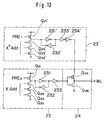
- the row decode circuit 23, the predecode circuit 23' (refer to Fig. 12) and the word line driving circuit 24 use Vpp as the power source and select and drive word lines to the booster level.
- Fig. 12 shows the details thereof.
- the row decode circuit 23 is constituted by a circuit where a P-channel MOS transistor Q21 on the gate of which a signal PRE 2 at the booster level is applied is connected in series to N-channel transistors Q22, Q23 and Q24 on the gates of which a row address signal X Add at the logic level is applied and three inverter circuits 231, 232 and 233.
- the predecode circuit 23' is constituted by a circuit where a P-channel MOS transistor Q21' on the gate of which a signal PRE 1 at the booster level is applied is connected in series to N-channel MOS transistors Q22', Q23' and Q24' on the gates of which a row address signal X+ Add at the logic level is applied and four inverter circuits 231', 232', 233' and 234'.
- the word line driving circuit 24 is constituted by inverter circuits Q25 and Q26 which use Vpp as the power source.
- the output terminal of the booster circuit and the respective signal lines of ⁇ E1,fE2,fT1 and ⁇ T2 are commonly connected via P-channel MOS transistors on pull-up side at the final stage of inverters (constituted by P-channel MOS transistor and N-channel MOS transistor) in the drive circuits 221 and 212. Further, these respective signal lines simultaneously drive a great number of bit line pairs (several hundreds) in the memory cell arrays and accordingly, the parasitic capacitance is very large. As a result it is possible to make comparatively small the capacitance of the de-coupling capacitor DC.
- the signal eMCA1 is changed from low level to high level (VDD) and the signal eMCA2 is maintained at low level.
- the potentials of N11, N12, N21 and N22 are respectively at Vss, Vpp, Vpp and Vss.
- the signals are amplified at the drive circuits 211 and 212 and ⁇ E1,fE2,fT1 and ⁇ T2 respectively become Vpp, Vss, Vpp and Vss.
- the sense amplifier S/A and the first memory cell array MCA1 are disconnected from each other and the equalizing operation of the right equalizing circuit is released.
- the word line WL is driven to the booster level by the operation of the word line driving circuit 24 and the operation such as reading is performed by the operation of the sense amplifier S/A.
- Fig. 3 shows an outline structural view of a DRAM of the present invention.
- the total memory capacity is assumed to be that of a 64M bit DRAM.
- Core blocks CB0, CB1, CB2 and CB3 each constituted by 16M bit memory cells and peripheral circuits within a core section such as sense amplifiers, decoders and the like accompanying the memory cells, are arranged in a semiconductor chip 9.
- Vpp generating circuits Vpp Pump each generating the boosted voltage Vpp of a word line, are respectively arranged between CB0 and CB1, and CB2 and CB3.
- Data multiplexer circuits MUX and data buffer circuits DIB are respectively arranged at data output units of the respective core blocks CB.
- Fuse arrays CFUSE for holding replaced data of column redundancy circuits are arranged at the vicinities of the respective core blocks.
- a reference voltage generating circuit VREF for generating a reference potential that is an intermediate potential of 1/2 Vcc etc. is arranged between CB0 and CB1.
- a power-on reset circuit PWRON for generating an initializing signal when the internal portion of the chip is initialized in case where power source is on, is arranged between CB2 and CB3.
- a substrate potential generation circuit SSB, a data input/output buffer I/O buffer and Pad, a IO data multiplexer circuit X1MUX for selecting Pad in accordance with data output width are successively arranged between CB0 and CB2.
- a self refresh control circuit'Self refresh, an address buffer Address buffer, a row series control circuit RAS series and a data control circuit DCC are successively arranged between CB1 and CB3. Further, column partial decoder circuits CPD, an address transition detection circuit ATD, a row partial decoder circuit RPD and a column address switch circuit ASD are respectively arranged at the central portion of the chip.
- Fig. 4 shows the structure of the 16M bit core block CB.
- 32 sets of memory cell arrays Cell and 33 sets of peripheral circuits within a core section S/A are alternately arranged constituting the memory cell block and the column decoder circuits C/D are arranged at an end thereof.
- a plurality of column select lines CSL are arranged in the column direction, and are selectively driven by the column decoder circuits C/D.
- the column select lines CSL supply selection signals to the peripheral circuits within a core section S/A at each column belonging to the same row. More in details the column select line is used for partial activation of the sense amplifier circuits and for driving the column gate circuits.
- the memory cell block constitutes the 16M bits core block CB by dividing it into top and bottom groups between which respectively arranged are row decoder circuits R/D(23) each corresponding to each memory cell array, circuits WDRV for supplying drive signals to the row decoder circuits, circuits RFUSE for holding replaced data of row redundancy circuits, data line amplifying circuits DQB, a block control circuit BC and the like.
- P-channel type sense amplifier drive circuits PSAD each corresponding to each peripheral circuit within a core section are respectively arranged at peripheral portions of the core blocks CB.
- the memory cell arrays MCA1 and MCA2 shown in Fig. 1 and Fig. 2 respectively correspond to the memory cell arrays Cell in Fig. 4.
- one 16M core block CB has 64 of the memory cell arrays Cell (MCA) and a single chip has 256 of the memory cell arrays Cell (MCA).
- MCA memory cell arrays Cell
- MCA memory cell arrays Cell
- the number of the transmission gate circuits in a single chip is 262144.
- a single transmission gate circuit is constituted by two N-channel transistors. Therefore, the number of the MOS transistors in the transmission gate circuits is 524288.
- the gate width of 0.8mm and the gate length of 0.56 ⁇ m in one MOS transistor the area of the channel regions in one MOS transistor is 0.45 ⁇ m 2 . By multiplying the area to all the MOS transistors the area amounts to 234880 ⁇ m 2 . Assuming the gate oxide film thickness of 12nm, it corresponds to a parasitic capacitance of 0.68nF.
- a single equalizing circuit is constituted by three MOS transistors, that is, two MOS transistors each having the gate width of 0.8 ⁇ m and the gate length of 0.56 ⁇ m and one MOS transistor having the gate width of 2.0 ⁇ m and the gate length of 0.56 ⁇ m. Accordingly, when the area is multiplied to all the MOS transistors, the total area of the channel regions amounts to 528482 ⁇ m 2 . This corresponds to a parasitic capacitance of 1.52nF.
- the parasitic capacitance calculated as above amounts to approximately 2.2nF. Normally several (4 in a refresh cycle product having 8K and 8 in a refresh cycle product having 4K) memory cell arrays are selected in reading. Therefore, substantially all of the memory cell arrays contribute to the parasitic capacitance. Further, in a 64M DRAM, a de-coupling capacitor DC having a capacitance of approximately 5nF is necessary to guarantee a stable operation. However, it is possible to approximately halve it to 2.8nF by the circuit structure of the present invention which contributes to a considerable reduction in the chip area.
- the memory device is divided into a number of memory cell arrays as in a DRAM having a large capacity and a ratio of the number of the memory cell arrays that are simultaneously activated to a total thereof is reduced by which the total amount of the parasitic capacitance can be increased which as a result contributes to the considerable reduction in the chip area.
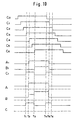
- Fig. 5 shows the circuit structure of the booster circuit VPPGEN.
- the booster circuit is constituted by a reference potential generating circuit 50, comparing circuits 51,52 and 53, ring oscillator circuits 54,55 and 56, driver circuits 57,58 and 59, charge pump circuits 60,61 and 62, voltage dividing circuits 63,64 and 65 and a power source voltage step-down transistor Q66.
- an outer potential Vcc inputted from the outside is stepped down by the power source voltage step-down transistor Q66 whereby VDD is generated and VDD is again boosted by the charge pump circuits 60 and 61 whereby the boosted potential Vpp is generated.
- the power source voltage step-down transistor Q66 is driven by VPPD that is a potential boosted from VDD. Further, the generation of Vpp is performed by two kinds of systems, that is, a system exclusive for standby and a system exclusive for operation. In this way the booster circuit is constituted by three booster systems each performing the boosting operation independently by a feedback type control.
- Fig. 6 shows behaviors of changes of Vpp, VPPD and VDD with respect to Vcc along with those of a cell capacitor plate potential VPL, a bit line potential VBL and a substrate potential VBB. There is a nonvariational region of potentials between approximately 3V to approximately 4V.
- Fig. 7 shows the detail of the ring oscillator 54 and a portion of the driver circuit 57.
- a NAND gate 541 and even number stages of inverters 542, 543, 544, 545, 546 and 547 are connected in a ring-like form.
- inverter circuits 571,572, 573, 574, 575, 576, 578, 579, 580, 581, 582, 583 and 584 are connected in series respectively forming successively delayed signal outputs /C0, C0, /C1, C1, /C2, C2, /C3, C3, /C4, C4, /C5, C5, /C6 and C6.
- Fig. 8 shows the remaining portion of the driver circuit 57.
- a signal A1 is formed from the signals C1 and C4 by a NAND gate 585 and inverters 586, 587 and 589.
- a signal B1 is formed from the signals C1 and C6 by a NAND gate 590 and inverters 591, 592 and 593.
- a signal C11 is formed from the signals C3, /C6,C2 and /C0 by a ANDNOR gate 604 and inverters 605, 606 and 607.
- a signal C12 is formed from the signals C3,/C6,C2 and/C0 by an ORNAND gate 608 and inverters 609,610,611 and 612.
- a signal A2 is formed from the signals C1 and C4 by a NOR gate 594 and inverters 595, 596, 597 and 598.
- a signal B2 is formed from the signals C1 and C6 by a NOR gate 599 and inverters 600, 601, 602 and 603.
- Fig. 9 shows the details of the charge pump circuit.
- the charge pump circuit is constituted by capacitors Q31,Q32,Q33,Q34,Q41 and Q42 and N-channel MOS transistors Q35, Q36, Q37,Q38,Q39 and Q40.
- Fig. 10 shows the operation of the charge pump circuit.
- the charge pump circuit is constituted by vertically symmetrical circuit portions, the explanation will be given only of the upper half portion for simplicity. To simplify the explanation no parasitic capacitance is considered and the capacitor coupling ratio is assumed to be infinitive.
- the signals C0 through C6 are provided with waveforms as shown in Fig. 10 by the driver circuit 57. At the initial state where one cycle operation has finished, a node A and a node B are provided with the potential of VDD and a node C is provided with the potential of 2VDD.
- the signal C1 is changed from Vss to VDD, then the potential of the node C is boosted from 2VDD to 3VDD by the capacitive connection of the capacitor Q41.
- the signal A1 is changed from Vss to VDD, then the potential of the node A is boosted from VDD to 2VDD by the capacitive connection of the capacitor Q31.
- 3VDD is supplied on the gate of the MOS transistor Q39 and accordingly, the potential of 2VDD is transmitted to the node B.
- the signal B1 is changed from Vss to VDD, then the potential of the node B is boosted from 2VDD to 3VDD by the capacitive connection of the capacitor Q33.
- the MOS transistor Q39 is cut off.
- the MOS transistor Q35 on the gate of which 3VDD is applied becomes conductive and 2VDD at the node A is transmitted to the Vpp node that is an output node.
- C1 again rises, at a time point t5, the potentials of A1 and B1 change from VDD to Vss and at a time point t6, C1 falls.
- the potential C1 is made VDD and the potential of the node C is made 3VDD before and after the time point t5 for finishing the boosting and transmitting operation to firmly initialize the potential of the node B to VDD.
- Vpp is approximately 4.3V for 3V of VDD by a feedback control and by the parasitic capacitance.
- the charge pump is very efficient compared with a conventional one.
- highfrequency noises are apt to generate therein and accordingly, it is necessary to connect the de-coupling capacitor DC having a large capacitance to output terminals. Therefore, the characteristic of the charge pump shown in Fig. 9 can be maximized by positively utilizing the parasitic capacitance by using the control system shown in Fig. 2.
- the present invention is not restricted to the above-mentioned structures and various modifications can naturally be performed so far as these modifications do not deviate from the gist of the invention.
- Vcc that is a power source potential inputted from the outside may directly be boosted whereby an effect of simplifying the power source circuit is achieved.
- the capacitance of the de-coupling capacitor can be reduced thereby contributing to the reduction in chip area.
- the capacitance of a de-coupling capacitor can further be reduced in case where a number of memory cell arrays are arranged and only a portion of the arrays are activated.
Description
- The conventional DRAM has utilized boot-strap-type word line driving circuits, which use N channel MOS transistors as word line drivers in word line driving circuits. This technology is disclosed in IEEE ISSCC DIGEST OF TECHNICAL PAPERS PP12-13 February 16, 1977. Meanwhile, reduction of power supply voltage and advancement of micro lithography technology have realized an arrangement of P channel type MOS transistors as word line drivers on every word line. Therefore a newly developed 64M bit DRAM has word line driving circuits each of which has a P channel MOS transistor, and a booster circuit to generate a word line driving voltage, which cause no threshold voltage drop of the word line driving voltage across the P channel MOS transistor.
- However, if a booster circuit is formed in a chip, a capacitor which is connected to the output of the booster circuit occupies a very large area in order to stabilize the output potential. Accordingly, a conventional DRAM with built-in booster circuit has a problem of chip area increase.
- US-A-5,267,214 and JP06-203600 disclose dynamic random access memory arrangements including a sense amplifier band shared between two different memory blocks. In this memory, only sense amplifiers related to a selected memory block are activated. The memory comprises a circuit for boosting a control signal voltage to a switching unit for connecting the selected memory block to the sense amplifiers up to a level higher than a power supply voltage Vcc during the activation of the sense amplifiers, and a circuit for separating a memory block paired with the selected memory block from the activated sense amplifiers during the sensing operation. The memory further comprises a circuit for generating a control signal of the power supply voltage Vcc and connecting all the memory blocks to the corresponding sense amplifiers in a stand-by state so as to reduce power consumption arising from the charge and discharge of the parasitic capacitance of the separating circuit. These documents do not disclose the use of stabilising capacitors at the output of the booster circuit.
- The present invention relates to a semiconductor memory, more particularly, to a DRAM (dynamic type random access memory) of a shared sense amplifier structure, which includes a booster circuit for generating a stationary boosted potential as a word line driving potential.
- It is an object of the present invention to minimize a capacitor area for potential stabilising capacitors which are connected to an output of a word line driving potential booster circuit.
- This object is achieved by the arrangement of
claim 1. - To achieve the above object, according to a further embodiment of the present invention there is provided a semiconductor memory device comprising: a booster circuit generating a boosted potential; a first memory cell array including first pairs of bit lines; a second memory cell array including second pairs of bit lines; a sense amplifier circuit; a first transmission gate circuit having pairs of transistors for connecting the first pairs of bit lines to the sense amplifier circuit; a second transmission gate circuit having pairs of transistors for connecting the second pairs of bit lines to the sense amplifier circuit; a first equalizing circuit having transistors equalizing the first pairs of bit lines; a second equalizing circuit having transistors equalizing the second pairs of bit lines; and a control circuit applying the boosted voltage respectively to gates of the transistors in the first and the second transmission gate circuits and gates of the transistors in the first and the second equalizing circuits when none of memory cells in the first and the second memory cell arrays is selected.
- By using the means provided by the present invention the boosted potential is applied on the gates of the transistors in the first and the second transmission gate circuits when none of the memory cells of the first and the second memory cell arrays is selected. That is, at this moment these transistors work as capacitive elements to be connected to the output of the booster circuit. Accordingly, the capacitance to be connected to the output of the booster circuit can be reduced by an amount corresponding to the parasitic capacitance of these transistors. Further, even when the memory cells in either of the first and the second memory cell arrays are selected, a half of the transistors in the transmission gate circuits are connected to the output of the booster circuit, the half work as capacitive elements and the capacitance to be connected to the booster circuit can be reduced by an amount corresponding to their parasitic capacitance.
- As stated above the transistors of the transmission gates and the like which have conventionally been connected to the ground potential in a nonselection time, are used as the capacitor for the booster circuit by which the area of the capacitive elements can be reduced by an amount corresponding to the parasitic capacitance.
- Other objects, features, and advantages of the present invention will become apparent from the following detailed description. It should be understood, however, that the detailed description and specific examples, while indicating preferred embodiments of the invention, are given by way of illustration only, since various changes and modifications within the scope of the invention will become apparent to those skilled in the art from this detailed description.
- A more complete appreciation of the present invention and many of its attendant advantages will be readily obtained by reference to the following detailed description considered in connection with the accompanying drawings, in which:
- Fig. 1 is a circuit diagram of the semiconductor memory of the present invention showing essential parts, and an operation diagram thereof;
- Fig. 2 is a circuit diagram of the semiconductor memory, showing more details of the essential part in Figure 1 and the control circuit thereof;
- Fig. 3. is an entire circuit configuration diagram of the embodiment of the present invention;
- Fig. 4 is a plane view of the semiconductor memory device of the embodiments of the present invention, showing details of the essential parts of Fig.3;
- Fig. 5 is a structural diagram of a booster circuit of a semiconductor memory device of the embodiments ;
- Fig. 6 is a view showing operational characteristic of the booster circuit of Fig. 5;
- Fig. 7 is a circuit diagram showing in details the booster circuit of Fig. 5;
- Fig. 8 is a circuit diagram showing in details the booster circuit of Fig. 5 ;
- Fig. 9 is a circuit diagram showing in details the booster circuit of Fig. 5;
- Fig. 10 is an operation diagram of the circuits shown in Figs. 7, 8 and 9;
- Fig. 11 is a plane view showing locations of de-coupling capacitors; and
- Fig. 12 is a circuit diagram showing in details a word line driving circuit and a row decode circuit.
-
- Embodiments of the present invention will be described in detail with reference to the drawings.
- Although the present invention is naturally applicable to various semiconductor memory devices ( SRAM, EPROM, MROM etc.) the explanation will be given of a DRAM since the present invention is preferable to a DRAM.
- Fig. 1 shows essential parts of the present invention which are constituted by a first memory cell array MCA1, a second memory cell array MCA2, a pair of left bit lines BLL and /BLL, a pair of right bit lines BLR and /BLR, a sense amplifier S/A and the like. Further, the embodiment includes a left bit line pair equalizing circuit constituted by N-channel MOS transistors Q1, Q2 and Q3, a left transmission gate constituted by N-channel MOS transistors Q4 and Q5, a right bit line pair equalizing circuit constituted by N-channel MOS transistors Q6, Q7 and Q8 and a right transmission gate circuit constituted by N-channel MOS transistors Q9 and Q10. A plurality of dynamic type memory cells are arranged in a matrix in each of the memory cell arrays MCA1 and MCA2. The memory cells belonging to the same column are connected by the same pair of bit lines and the memory cells belonging to the same row are connected by the same word line. The left bit line pair equalizing circuit is controlled by a signal E1. When E1 is at a boosted potential Vpp ( for example, 4.3V in comparison with ground potential ), VBL (for example, 1.5V which is about a half of potential of VDD that is an inner power source potential ) is supplied to the left bit line pair BLL and /BLL and the both are shortcircuited. When E1 is at a ground potential Vss (0V) all the MOS transistors in the circuit are made nonconductive. The right bit line pair equalizing circuit is controlled by a signal E2. When E2 is at the boosted potential Vpp, VBL is supplied to the right bit line pair BLR and /BLR and the both are shortcircuited. When E2 is at the ground potential Vss, all the MOS transistors in the circuit are made nonconductive. The left transmission gate circuit is controlled by a signal T2. When T2 is at the boosted potential Vpp, the left bit line pair BLL and/BLL is connected to the sense amplifier S/A . When T2 is at the ground potential Vss, the left bit line pair BLL and /BLL and the sense amplifier S/A are disconnected from each other. The right transmission gate circuit is controlled by a signal T1. When T1 is at the boosted potential Vpp, the right bit line pair BLR and /BLR are connected to the sense amplifier S/A. When T1 is at the ground potential Vss, the right bit line pair BLR and/BLR and the sense amplifier S/A are disconnected from each other.
- In the above-constituted DRAM when none of the memory cells in the first and the second memory cell arrays is selected, all of E1, E2, T1, T2 are connected to Vpp. Since a word line, not shown, is in a nonselect state, data stored in the memory cells are not destructed. At this moment all the MOS transistors Q1 through Q10 in Fig. 1 are connected to Vpp and accordingly, the transistors provide a parasitic capacitance connected in parallel to capacitive elements that are to be connected to output terminals of a booster circuit, not shown, by which the capacitive elements can be made smaller by the amount of the parasitic capacitance.
- When the memory cells in the first memory cell array are selected, as shown in Fig. 1, E1 is changed from Vpp to Vss, T2 is maintained as Vpp, T1 is changed from Vpp to Vss and E2 is maintained as Vpp by which the sense amplifier S/A and the second memory cell array MCA2 are disconnected from each other and the equalizing operation of the left equalizing circuit is released.
- When the memory cells in the second memory cell array are selected, in a similar way, E1 is maintained as Vpp, T2 is changed from Vpp to Vss, T1 is maintained as Vpp and T2 is changed from Vpp to Vss by which the sense amplifier S/A and the first memory cell array MCA1 are disconnected from each other and the equalizing operation of the right equalizing circuit is released.
- As stated above by using the transistors of the transmission gates and the like which have conventionally been connected to the ground potential in a nonselect time as a capacitor of the booster circuit, the area of the capacitive elements can be reduced by the amount of their parasitic capacitance.
- Next, Fig. 2 shows essential parts of the present invention and the details of a control system. The control system is constituted by a booster circuit VPPGEN generating the boosted potential Vpp from an inner power source potential VDD, a capacitor DC (hereinafter, de-coupling capacitor), a
circuit 221 for selecting and driving MCA1 which includes a firstlevel shift circuit 201 and afirst drive circuit 211, acircuit 222 for selecting and driving MCA2 which includes a second level shift circuit 202 and a second drive circuit 212, arow decode circuit 23, a wordline driving circuit 24 and the like. - The
level shift circuits 201 and 202 respectively use Vpp as a power source and shift eMCA1 and eMCA2 which are output signals of a memory cell array select circuit, not shown, from a logic level (amplitude between Vss-VDD) to a boost level ( amplitude between Vss-Vpp). Thedrive circuits - The
row decode circuit 23, the predecode circuit 23' (refer to Fig. 12) and the wordline driving circuit 24 use Vpp as the power source and select and drive word lines to the booster level. Fig. 12 shows the details thereof. Therow decode circuit 23 is constituted by a circuit where a P-channel MOS transistor Q21 on the gate of which asignal PRE 2 at the booster level is applied is connected in series to N-channel transistors Q22, Q23 and Q24 on the gates of which a row address signal X Add at the logic level is applied and threeinverter circuits signal PRE 1 at the booster level is applied is connected in series to N-channel MOS transistors Q22', Q23' and Q24' on the gates of which a row address signal X+ Add at the logic level is applied and four inverter circuits 231', 232', 233' and 234'. The wordline driving circuit 24 is constituted by inverter circuits Q25 and Q26 which use Vpp as the power source. - Next, an explanation will be given of the operation of the circuit shown in Fig. 2. When both of MCA1 and MCA2 are not selected, the signal eMCA1 and the signal eMCA2 are both at LOW level (Vss). At this moment the potentials of N11, N12, N21 and N22 are respectively at Vpp, Vss, Vpp and Vss. The signals are amplified by the amplifying
circuits 211 and 212 and all of E1, fE2, fT1 and T2 are at Vpp. Here, the output terminal of the booster circuit and the respective signal lines of E1,fE2,fT1 and T2 are commonly connected via P-channel MOS transistors on pull-up side at the final stage of inverters (constituted by P-channel MOS transistor and N-channel MOS transistor) in thedrive circuits 221 and 212. Further, these respective signal lines simultaneously drive a great number of bit line pairs (several hundreds) in the memory cell arrays and accordingly, the parasitic capacitance is very large. As a result it is possible to make comparatively small the capacitance of the de-coupling capacitor DC. - Next, the operation in case where MCA2 is selected is shown as an example. The signal eMCA1 is changed from low level to high level (VDD) and the signal eMCA2 is maintained at low level. As a result, the potentials of N11, N12, N21 and N22 are respectively at Vss, Vpp, Vpp and Vss. The signals are amplified at the
drive circuits 211 and 212 and E1,fE2,fT1 and T2 respectively become Vpp, Vss, Vpp and Vss. As a result the sense amplifier S/A and the first memory cell array MCA1 are disconnected from each other and the equalizing operation of the right equalizing circuit is released. Successively, the word line WL is driven to the booster level by the operation of the wordline driving circuit 24 and the operation such as reading is performed by the operation of the sense amplifier S/A. - A similar operation is performed when MCA1 is selected and accordingly,the explanation will be omitted.
- Fig. 3 shows an outline structural view of a DRAM of the present invention. The total memory capacity is assumed to be that of a 64M bit DRAM. Core blocks CB0, CB1, CB2 and CB3 each constituted by 16M bit memory cells and peripheral circuits within a core section such as sense amplifiers, decoders and the like accompanying the memory cells, are arranged in a
semiconductor chip 9. Vpp generating circuits Vpp Pump each generating the boosted voltage Vpp of a word line, are respectively arranged between CB0 and CB1, and CB2 and CB3. Data multiplexer circuits MUX and data buffer circuits DIB are respectively arranged at data output units of the respective core blocks CB. Fuse arrays CFUSE for holding replaced data of column redundancy circuits are arranged at the vicinities of the respective core blocks. A reference voltage generating circuit VREF for generating a reference potential that is an intermediate potential of 1/2 Vcc etc. is arranged between CB0 and CB1. A power-on reset circuit PWRON for generating an initializing signal when the internal portion of the chip is initialized in case where power source is on, is arranged between CB2 and CB3. A substrate potential generation circuit SSB, a data input/output buffer I/O buffer and Pad, a IO data multiplexer circuit X1MUX for selecting Pad in accordance with data output width are successively arranged between CB0 and CB2. A self refresh control circuit'Self refresh, an address buffer Address buffer, a row series control circuit RAS series and a data control circuit DCC are successively arranged between CB1 and CB3. Further, column partial decoder circuits CPD, an address transition detection circuit ATD, a row partial decoder circuit RPD and a column address switch circuit ASD are respectively arranged at the central portion of the chip. - Next, Fig. 4 shows the structure of the 16M bit core block CB. 32 sets of memory cell arrays Cell and 33 sets of peripheral circuits within a core section S/A are alternately arranged constituting the memory cell block and the column decoder circuits C/D are arranged at an end thereof. A plurality of column select lines CSL are arranged in the column direction, and are selectively driven by the column decoder circuits C/D. The column select lines CSL supply selection signals to the peripheral circuits within a core section S/A at each column belonging to the same row. More in details the column select line is used for partial activation of the sense amplifier circuits and for driving the column gate circuits. The memory cell block constitutes the 16M bits core block CB by dividing it into top and bottom groups between which respectively arranged are row decoder circuits R/D(23) each corresponding to each memory cell array, circuits WDRV for supplying drive signals to the row decoder circuits, circuits RFUSE for holding replaced data of row redundancy circuits, data line amplifying circuits DQB, a block control circuit BC and the like. P-channel type sense amplifier drive circuits PSAD each corresponding to each peripheral circuit within a core section are respectively arranged at peripheral portions of the core blocks CB.
- The memory cell arrays MCA1 and MCA2 shown in Fig. 1 and Fig. 2 respectively correspond to the memory cell arrays Cell in Fig. 4. As is illustrated one 16M core block CB has 64 of the memory cell arrays Cell (MCA) and a single chip has 256 of the memory cell arrays Cell (MCA). The following description indicates how much parasitic capacitance is provided by the block structure shown in Fig. 3 and Fig. 4 and how much capacity of the de-coupling capacitor can be saved as a result.
- First, a contribution of the transmission gate circuits will be calculated. There are 1024 pairs of bit lines in one memory cell array ( disregarding redundancy bit lines). Therefore, the number of the transmission gate circuits in a single chip is 262144. Incidently, a single transmission gate circuit is constituted by two N-channel transistors. Therefore, the number of the MOS transistors in the transmission gate circuits is 524288. For example, assuming the gate width of 0.8mm and the gate length of 0.56µm in one MOS transistor, the area of the channel regions in one MOS transistor is 0.45µm2. By multiplying the area to all the MOS transistors the area amounts to 234880µm2. Assuming the gate oxide film thickness of 12nm, it corresponds to a parasitic capacitance of 0.68nF.
- Secondly, a contribution of the equalizing circuits will be calculated. The number of the equalizing circuits in a single memory cell array is also 262144. A single equalizing circuit is constituted by three MOS transistors, that is, two MOS transistors each having the gate width of 0.8µm and the gate length of 0.56µm and one MOS transistor having the gate width of 2.0µm and the gate length of 0.56µm. Accordingly, when the area is multiplied to all the MOS transistors, the total area of the channel regions amounts to 528482µm2. This corresponds to a parasitic capacitance of 1.52nF.
- The parasitic capacitance calculated as above amounts to approximately 2.2nF. Normally several (4 in a refresh cycle product having 8K and 8 in a refresh cycle product having 4K) memory cell arrays are selected in reading. Therefore, substantially all of the memory cell arrays contribute to the parasitic capacitance. Further, in a 64M DRAM, a de-coupling capacitor DC having a capacitance of approximately 5nF is necessary to guarantee a stable operation. However, it is possible to approximately halve it to 2.8nF by the circuit structure of the present invention which contributes to a considerable reduction in the chip area.
- In this way, the memory device is divided into a number of memory cell arrays as in a DRAM having a large capacity and a ratio of the number of the memory cell arrays that are simultaneously activated to a total thereof is reduced by which the total amount of the parasitic capacitance can be increased which as a result contributes to the considerable reduction in the chip area.
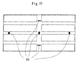
- Further, as shown in Fig. 11 the de-coupling capacitors DC are scattered all over the tip.
- Next, a detailed explanation will be given of the booster circuit VPPGEN in reference to Fig. 5 through Fig. 10.
- Fig. 5 shows the circuit structure of the booster circuit VPPGEN. The booster circuit is constituted by a reference
potential generating circuit 50, comparingcircuits ring oscillator circuits driver circuits charge pump circuits voltage dividing circuits charge pump circuits - Fig. 6 shows behaviors of changes of Vpp, VPPD and VDD with respect to Vcc along with those of a cell capacitor plate potential VPL, a bit line potential VBL and a substrate potential VBB. There is a nonvariational region of potentials between approximately 3V to approximately 4V.
- Fig. 7 shows the detail of the
ring oscillator 54 and a portion of thedriver circuit 57. In the ring oscillator 54 aNAND gate 541 and even number stages ofinverters - Fig. 8 shows the remaining portion of the
driver circuit 57. A signal A1 is formed from the signals C1 and C4 by aNAND gate 585 andinverters NAND gate 590 andinverters ANDNOR gate 604 andinverters ORNAND gate 608 and inverters 609,610,611 and 612. A signal A2 is formed from the signals C1 and C4 by a NORgate 594 andinverters gate 599 andinverters - Fig. 9 shows the details of the charge pump circuit. The charge pump circuit is constituted by capacitors Q31,Q32,Q33,Q34,Q41 and Q42 and N-channel MOS transistors Q35, Q36, Q37,Q38,Q39 and Q40.
- Fig. 10 shows the operation of the charge pump circuit. Although the charge pump circuit is constituted by vertically symmetrical circuit portions, the explanation will be given only of the upper half portion for simplicity. To simplify the explanation no parasitic capacitance is considered and the capacitor coupling ratio is assumed to be infinitive. The signals C0 through C6 are provided with waveforms as shown in Fig. 10 by the
driver circuit 57. At the initial state where one cycle operation has finished, a node A and a node B are provided with the potential of VDD and a node C is provided with the potential of 2VDD. At a time point t1, the signal C1 is changed from Vss to VDD, then the potential of the node C is boosted from 2VDD to 3VDD by the capacitive connection of the capacitor Q41. At a time point t2, the signal A1 is changed from Vss to VDD, then the potential of the node A is boosted from VDD to 2VDD by the capacitive connection of the capacitor Q31. 3VDD is supplied on the gate of the MOS transistor Q39 and accordingly, the potential of 2VDD is transmitted to the node B. Successively at a time point t3, the signal B1 is changed from Vss to VDD, then the potential of the node B is boosted from 2VDD to 3VDD by the capacitive connection of the capacitor Q33. At this instance the MOS transistor Q39 is cut off. As a result the MOS transistor Q35 on the gate of which 3VDD is applied becomes conductive and 2VDD at the node A is transmitted to the Vpp node that is an output node. At a time point t4, C1 again rises, at a time point t5, the potentials of A1 and B1 change from VDD to Vss and at a time point t6, C1 falls. The potential C1 is made VDD and the potential of the node C is made 3VDD before and after the time point t5 for finishing the boosting and transmitting operation to firmly initialize the potential of the node B to VDD. - As explained above theoretically 2VDD is stationarily outputted. However, actually Vpp is approximately 4.3V for 3V of VDD by a feedback control and by the parasitic capacitance. The charge pump is very efficient compared with a conventional one. However, highfrequency noises are apt to generate therein and accordingly, it is necessary to connect the de-coupling capacitor DC having a large capacitance to output terminals. Therefore, the characteristic of the charge pump shown in Fig. 9 can be maximized by positively utilizing the parasitic capacitance by using the control system shown in Fig. 2.
- Although detailed explanation has been given to the embodiments wherein the present invention is used in a 64M bit DRAM, the present invention is not restricted to the above-mentioned structures and various modifications can naturally be performed so far as these modifications do not deviate from the gist of the invention. Especially, with regard to the structure of the power source circuit, although the stepped-down potential VDD is further boosted in the above-mentioned embodiments, Vcc that is a power source potential inputted from the outside may directly be boosted whereby an effect of simplifying the power source circuit is achieved.
- According to the present invention the capacitance of the de-coupling capacitor can be reduced thereby contributing to the reduction in chip area. The capacitance of a de-coupling capacitor can further be reduced in case where a number of memory cell arrays are arranged and only a portion of the arrays are activated.
- While there has been illustrated and described what are presently considered to be preferred embodiments of the present invention, it will be understood by those skilled in the art that various changes and modifications may be made, and equivalents may be substituted for devices thereof without departing from the true scope of the invention. In addition many modifications may be made to adapt a particular situation or material to the teaching of the present invention without departing from the central scope thereof. Therefore, it is intended that this invention not be limited to the particular embodiment disclosed as the best mode contemplated for carrying out this invention, but that the invention include all embodiments falling within the scope of the appended claims.
Claims (10)
- A semiconductor memory device having:characterised in that capacitive elements (DC) are connected to the output terminal of the booster circuit.a booster circuit (VPPGEN) for generating a boosted potential (VPP) at an output terminal of said booster circuit;a first memory cell array (MCA1) including first pairs of bit lines (BLL1/BLL);a second memory cell array (MCAn) including second pairs of bit lines (BLR1/BLR);a sense amplifier circuit (S/A);a first transmission gate circuit (ØT2) having pairs of transistors (Q4, Q5) for connecting the first pairs of bit lines (BLL1/BLL) to the sense amplifier circuit (S/A);a second transmission gate circuit (ØT1) having pairs of transistors (Q9, Q10) for connecting the second pairs of bit lines (BLR1/BLR) to the sense amplifier circuit (S/A); anda control circuit (221) applying the boosted potential (VPP) respectively to gates of the transistors in the first and the second transmission gate circuits (ØT2, ØT1) when none of memory cells in the first and the second memory cell arrays (MCA1, MCA2) is selected,
- The semiconductor memory device of claim 1 further comprising:a first equalizing circuit (E1) having transistors (Q1, Q2, Q3) for equalizing the first pairs of bit lines (BLL1/BLL);a second equalizing circuit (ØE2) having transistors (Q6, Q7, Q8) for equalizing the second pairs of bit lines (BLR1/BLR); andwherein said control circuit (221) further applies the boosted voltage (CVPP) respectively to gates of the transistors in the first and the second equalizing circuits (E1, ØE2) when none of memory cells in the first and the second memory cell arrays (MCA1, MCA2) is selected.
- The semiconductor memory device according to claim 2, wherein the control circuit (221) applies a ground potential respectively to the gates of the transistors in the first equalizing circuit (ØE1) and to the gates of the transistors in the second transmission gate circuit (ØT1) and applies the boosted potential (VPP) respectively to the gates of the transistors in the second equalizing circuit (ØE2) and to the gates of the transistors in the first transmission gate circuit (ØT2) when selecting the memory cells in the first memory cell array (MCA1); and
wherein the control circuit (221) applies the ground potential respectively to the gates of the transistors in the second equalizing circuit (ØE2) and to the gates of the transistors in the first transmission gate circuit (ØE2) and applies the boosted potential (VPP) respectively to the gates of the transistors in the first equalizing circuit (ØE1) and to the gates of the transistors in the second transmit circuit (ØT1) when selecting the memory cells in the second memory cell array (MCA2). - The semiconductor memory device according to claim 1, wherein the control circuit (221) applies a ground potential to the gates of the transistors in the second transmission gate circuits (ØT1) and applies the boosted potential (VPP) to the gates of the transistors in the first transmission gate circuit (ØT2) when selecting the memory cells in the first memory cell array (MCA1); and
the control circuit (22) applies the ground potential to the gates of the transistors in the first transmission gate circuit (ØT2) and applies the boosted potential (VPP) to the gates of the transistors in the second transmission gate circuit (ØT1) when selecting the memory cells in the second memory cell array (MCA2). - The semiconductor memory device according to claim 2 or 4, wherein first and second word line driving circuits 24 are respectively connected to the first and the second memory cell arrays (MCA1/MCAn) and the first and the second word line driving circuits (24) are operated by the boosted potential (VPP).
- The semiconductor memory device according to claim 5, wherein the first and the second word line driving circuits (24) are controlled respectively based on selection signals of first and second row decode circuits (23) and the first and the second row decode circuits are operated by the boosted potential (VPP).
- The semiconductor memory device according to claim 2 or 6, wherein the control circuit (22) comprises at least a first level shift circuit (20) for shifting an amplitude level of a first select signal for selecting the first memory cell array to a level of the boosted potential and a second level shift circuit (202) for shifting an amplitude level of a second select signal for selecting the second memory cell array to the level of the boosted potential (VPP) and the boosted potential (VPP) is used for a power source of the first and the second level shift circuits.
- The semiconductor memory device according to claim 7, wherein the control circuit is further comprising first and second drive circuits (211, 212) respectively connected to the first and the second level shift circuits (201, 202), said first and second drive circuits using the boosted potential (VPP) as a power source and driving the gates of the transistors in the first and the second transmission gate circuits (ØT2, ØT1) to the boosted potential (VPP) when none of the memory cells in the first and the second memory cell arrays (MCA1, MCA2) is selected.
- The semiconductor memory device according to claim 1 or 2, wherein the booster circuit (VPPGEN) generates the boosted potential (VPP) by stepping down a potential inputted from an outside and again boosting the potential.
- The semiconductor memory device according to claim 7, wherein the control circuit (22) is further comprising first and second drive circuits (2Ø1, 2Ø2) respectively connected to the first and the second level shift circuits (201, 202), said first and second drive circuits (211, 212) using the boosted potential (VPP) as a power source and driving the gates of transistors in the first and the second transmission gate circuits (ØT2, ØT1) and the gates of transistors in the first and the second equalizing circuits (ØE1, ØE2) to the boosted potential (VPP) when none of the memory cells in the first and the second memory cell arrays (MCA1, MCA2) is selected.
Applications Claiming Priority (3)
| Application Number | Priority Date | Filing Date | Title |
|---|---|---|---|
| JP6312991A JPH08171796A (en) | 1994-12-16 | 1994-12-16 | Semiconductor storage |
| JP31299194 | 1994-12-16 | ||
| JP312991/94 | 1994-12-16 |
Publications (3)
| Publication Number | Publication Date |
|---|---|
| EP0717415A2 EP0717415A2 (en) | 1996-06-19 |
| EP0717415A3 EP0717415A3 (en) | 1999-08-25 |
| EP0717415B1 true EP0717415B1 (en) | 2003-04-09 |
Family
ID=18035927
Family Applications (1)
| Application Number | Title | Priority Date | Filing Date |
|---|---|---|---|
| EP95118297A Expired - Lifetime EP0717415B1 (en) | 1994-12-16 | 1995-11-21 | Semiconductor memory device |
Country Status (7)
| Country | Link |
|---|---|
| US (1) | US5740113A (en) |
| EP (1) | EP0717415B1 (en) |
| JP (1) | JPH08171796A (en) |
| KR (1) | KR0175704B1 (en) |
| CN (1) | CN1078730C (en) |
| DE (1) | DE69530266T2 (en) |
| TW (1) | TW301749B (en) |
Families Citing this family (16)
| Publication number | Priority date | Publication date | Assignee | Title |
|---|---|---|---|---|
| JP2825291B2 (en) * | 1989-11-13 | 1998-11-18 | 株式会社東芝 | Semiconductor storage device |
| JP2917914B2 (en) * | 1996-05-17 | 1999-07-12 | 日本電気株式会社 | Boost circuit |
| TW423162B (en) | 1997-02-27 | 2001-02-21 | Toshiba Corp | Power voltage supplying circuit and semiconductor memory including the same |
| JPH10302469A (en) * | 1997-04-25 | 1998-11-13 | Fujitsu Ltd | Semiconductor memory device |
| US6016279A (en) * | 1998-03-30 | 2000-01-18 | Vanguard International Semiconductor Corporation | DRAM sensing scheme and isolation circuit |
| US5870343A (en) * | 1998-04-06 | 1999-02-09 | Vanguard International Semiconductor Corporation | DRAM sensing scheme for eliminating bit-line coupling noise |
| US6009023A (en) * | 1998-05-26 | 1999-12-28 | Etron Technology, Inc. | High performance DRAM structure employing multiple thickness gate oxide |
| US6033945A (en) * | 1998-06-03 | 2000-03-07 | G-Link Technology | Multiple equilibration circuits for a single bit line |
| KR100532392B1 (en) * | 1998-08-28 | 2006-03-16 | 삼성전자주식회사 | Semiconductor memory device and isolation transistor control method to improve sensing speed in the early stage of sensing operation |
| JP2000298984A (en) * | 1999-04-15 | 2000-10-24 | Oki Electric Ind Co Ltd | Semiconductor memory |
| DE10107314C2 (en) | 2001-02-16 | 2003-03-27 | Infineon Technologies Ag | Method for reading a memory cell of a semiconductor memory and semiconductor memory |
| KR100518230B1 (en) * | 2003-06-16 | 2005-10-04 | 주식회사 하이닉스반도체 | A driving voltage driver for sense amplifier of memory device |
| JP4275583B2 (en) * | 2004-06-24 | 2009-06-10 | ユーディナデバイス株式会社 | Electronic module |
| WO2007029333A1 (en) * | 2005-09-09 | 2007-03-15 | Fujitsu Limited | Semiconductor integrated circuit |
| JP5259505B2 (en) | 2009-06-26 | 2013-08-07 | 株式会社東芝 | Semiconductor memory device |
| US9293192B1 (en) | 2014-12-02 | 2016-03-22 | International Business Machines Corporation | SRAM cell with dynamic split ground and split wordline |
Family Cites Families (8)
| Publication number | Priority date | Publication date | Assignee | Title |
|---|---|---|---|---|
| JPS6150284A (en) * | 1984-08-17 | 1986-03-12 | Mitsubishi Electric Corp | Driving method of shared sense amplifier circuit |
| JPS63257994A (en) * | 1987-04-15 | 1988-10-25 | Nec Corp | Semiconductor storage device |
| US5237534A (en) * | 1989-04-27 | 1993-08-17 | Kabushiki Kaisha Toshiba | Data sense circuit for a semiconductor nonvolatile memory device |
| JP2742719B2 (en) * | 1990-02-16 | 1998-04-22 | 三菱電機株式会社 | Semiconductor storage device |
| KR950009234B1 (en) * | 1992-02-19 | 1995-08-18 | 삼성전자주식회사 | Bit-line disconnection clock generating device of semiconductor memory device |
| US5291437A (en) * | 1992-06-25 | 1994-03-01 | Texas Instruments Incorporated | Shared dummy cell |
| JP2768172B2 (en) * | 1992-09-30 | 1998-06-25 | 日本電気株式会社 | Semiconductor memory device |
| KR950004870B1 (en) * | 1992-11-24 | 1995-05-15 | 삼성전자 주식회사 | Isolation gate circuit with improved reliability in burn-in mode |
-
1994
- 1994-12-16 JP JP6312991A patent/JPH08171796A/en active Pending
-
1995
- 1995-11-21 EP EP95118297A patent/EP0717415B1/en not_active Expired - Lifetime
- 1995-11-21 DE DE69530266T patent/DE69530266T2/en not_active Expired - Lifetime
- 1995-12-12 US US08/571,135 patent/US5740113A/en not_active Expired - Lifetime
- 1995-12-15 KR KR1019950050394A patent/KR0175704B1/en not_active IP Right Cessation
- 1995-12-15 CN CN95120907A patent/CN1078730C/en not_active Expired - Fee Related
-
1996
- 1996-02-01 TW TW085101267A patent/TW301749B/zh not_active IP Right Cessation
Also Published As
| Publication number | Publication date |
|---|---|
| US5740113A (en) | 1998-04-14 |
| CN1132396A (en) | 1996-10-02 |
| KR0175704B1 (en) | 1999-04-15 |
| DE69530266T2 (en) | 2003-12-04 |
| TW301749B (en) | 1997-04-01 |
| JPH08171796A (en) | 1996-07-02 |
| EP0717415A3 (en) | 1999-08-25 |
| DE69530266D1 (en) | 2003-05-15 |
| KR960025728A (en) | 1996-07-20 |
| EP0717415A2 (en) | 1996-06-19 |
| CN1078730C (en) | 2002-01-30 |
Similar Documents
| Publication | Publication Date | Title |
|---|---|---|
| KR100224960B1 (en) | Semiconductor integrated circuit | |
| EP0717415B1 (en) | Semiconductor memory device | |
| KR100201723B1 (en) | Memory device | |
| US6753720B2 (en) | Internal high voltage generation circuit capable of stably generating internal high voltage and circuit element therefor | |
| KR970000883B1 (en) | Semiconductor memory device having dual word line structure | |
| US6489796B2 (en) | Semiconductor device provided with boost circuit consuming less current | |
| US7764560B2 (en) | Semiconductor memory device and refresh method for the same | |
| US5335205A (en) | DRAM using word line potential control circuitcircuit | |
| KR100621554B1 (en) | Semiconductor memory device | |
| US7046572B2 (en) | Low power manager for standby operation of memory system | |
| KR0164377B1 (en) | Sub-word line driver | |
| US5699289A (en) | Power source circuit and wiring group for semiconductor memory device | |
| JPH09134592A (en) | Subword line decoder of semiconductor memory and its semiconductor memory | |
| EP0741386B1 (en) | Decoder and decoder driver with voltage level translator | |
| US5774405A (en) | Dynamic random access memory having an internal circuit using a boosted potential | |
| US5668485A (en) | Row decoder with level translator | |
| US20200402565A1 (en) | Apparatuses and methods for controlling word line discharge | |
| US5291450A (en) | Read circuit of dynamic random access memory | |
| US5933388A (en) | Sub row decoder circuit for semiconductor memory device | |
| US5555206A (en) | Semiconductor memory device | |
| US6104659A (en) | Memory device | |
| US5777934A (en) | Semiconductor memory device with variable plate voltage generator | |
| US5596533A (en) | Method and apparatus for reading/writing data from/into semiconductor memory device | |
| US8363489B2 (en) | Semiconductor device having bit line equalization using low voltage and a method thereof | |
| JP2000036193A (en) | Semiconductor integrated circuit device |
Legal Events
| Date | Code | Title | Description |
|---|---|---|---|
| PUAI | Public reference made under article 153(3) epc to a published international application that has entered the european phase |
Free format text: ORIGINAL CODE: 0009012 |
|
| AK | Designated contracting states |
Kind code of ref document: A2 Designated state(s): DE FR GB |
|
| PUAL | Search report despatched |
Free format text: ORIGINAL CODE: 0009013 |
|
| AK | Designated contracting states |
Kind code of ref document: A3 Designated state(s): DE FR GB |
|
| RIC1 | Information provided on ipc code assigned before grant |
Free format text: 6G 11C 11/409 A, 6G 11C 7/06 B |
|
| 17P | Request for examination filed |
Effective date: 19990921 |
|
| 17Q | First examination report despatched |
Effective date: 20010530 |
|
| GRAG | Despatch of communication of intention to grant |
Free format text: ORIGINAL CODE: EPIDOS AGRA |
|
| GRAG | Despatch of communication of intention to grant |
Free format text: ORIGINAL CODE: EPIDOS AGRA |
|
| GRAH | Despatch of communication of intention to grant a patent |
Free format text: ORIGINAL CODE: EPIDOS IGRA |
|
| GRAH | Despatch of communication of intention to grant a patent |
Free format text: ORIGINAL CODE: EPIDOS IGRA |
|
| GRAA | (expected) grant |
Free format text: ORIGINAL CODE: 0009210 |
|
| AK | Designated contracting states |
Designated state(s): DE FR GB |
|
| REG | Reference to a national code |
Ref country code: GB Ref legal event code: FG4D |
|
| ET | Fr: translation filed | ||
| PLBE | No opposition filed within time limit |
Free format text: ORIGINAL CODE: 0009261 |
|
| STAA | Information on the status of an ep patent application or granted ep patent |
Free format text: STATUS: NO OPPOSITION FILED WITHIN TIME LIMIT |
|
| 26N | No opposition filed |
Effective date: 20040112 |
|
| PGFP | Annual fee paid to national office [announced via postgrant information from national office to epo] |
Ref country code: DE Payment date: 20101117 Year of fee payment: 16 |
|
| PGFP | Annual fee paid to national office [announced via postgrant information from national office to epo] |
Ref country code: GB Payment date: 20101117 Year of fee payment: 16 |
|
| PGFP | Annual fee paid to national office [announced via postgrant information from national office to epo] |
Ref country code: FR Payment date: 20111118 Year of fee payment: 17 |
|
| GBPC | Gb: european patent ceased through non-payment of renewal fee |
Effective date: 20121121 |
|
| REG | Reference to a national code |
Ref country code: FR Ref legal event code: ST Effective date: 20130731 |
|
| REG | Reference to a national code |
Ref country code: DE Ref legal event code: R119 Ref document number: 69530266 Country of ref document: DE Effective date: 20130601 |
|
| PG25 | Lapsed in a contracting state [announced via postgrant information from national office to epo] |
Ref country code: DE Free format text: LAPSE BECAUSE OF NON-PAYMENT OF DUE FEES Effective date: 20130601 |
|
| PG25 | Lapsed in a contracting state [announced via postgrant information from national office to epo] |
Ref country code: GB Free format text: LAPSE BECAUSE OF NON-PAYMENT OF DUE FEES Effective date: 20121121 Ref country code: FR Free format text: LAPSE BECAUSE OF NON-PAYMENT OF DUE FEES Effective date: 20121130 |