EP0720287B1 - Wide dynamic range power amplifier - Google Patents
Wide dynamic range power amplifier Download PDFInfo
- Publication number
- EP0720287B1 EP0720287B1 EP95309095A EP95309095A EP0720287B1 EP 0720287 B1 EP0720287 B1 EP 0720287B1 EP 95309095 A EP95309095 A EP 95309095A EP 95309095 A EP95309095 A EP 95309095A EP 0720287 B1 EP0720287 B1 EP 0720287B1
- Authority
- EP
- European Patent Office
- Prior art keywords
- power
- output
- voltage
- output power
- input
- Prior art date
- Legal status (The legal status is an assumption and is not a legal conclusion. Google has not performed a legal analysis and makes no representation as to the accuracy of the status listed.)
- Expired - Lifetime
Links
Images
Classifications
-
- H—ELECTRICITY
- H03—ELECTRONIC CIRCUITRY
- H03G—CONTROL OF AMPLIFICATION
- H03G3/00—Gain control in amplifiers or frequency changers without distortion of the input signal
- H03G3/20—Automatic control
- H03G3/30—Automatic control in amplifiers having semiconductor devices
- H03G3/3036—Automatic control in amplifiers having semiconductor devices in high-frequency amplifiers or in frequency-changers
- H03G3/3042—Automatic control in amplifiers having semiconductor devices in high-frequency amplifiers or in frequency-changers in modulators, frequency-changers, transmitters or power amplifiers
- H03G3/3047—Automatic control in amplifiers having semiconductor devices in high-frequency amplifiers or in frequency-changers in modulators, frequency-changers, transmitters or power amplifiers for intermittent signals, e.g. burst signals
-
- H—ELECTRICITY
- H03—ELECTRONIC CIRCUITRY
- H03G—CONTROL OF AMPLIFICATION
- H03G3/00—Gain control in amplifiers or frequency changers without distortion of the input signal
- H03G3/20—Automatic control
- H03G3/30—Automatic control in amplifiers having semiconductor devices
- H03G3/3036—Automatic control in amplifiers having semiconductor devices in high-frequency amplifiers or in frequency-changers
- H03G3/3042—Automatic control in amplifiers having semiconductor devices in high-frequency amplifiers or in frequency-changers in modulators, frequency-changers, transmitters or power amplifiers
Definitions
- This invention relates to wide dynamic range power amplifiers, and to methods of changing the output power of a power amplifier.
- Power amplifiers are commonly used as general purpose transmitters for wireless base-stations and handsets. In these applications, the power amplifier serves to change the power of an incoming signal to an output power suitable for transmitting the signal over a communication medium, such as the electromagnetic frequency spectrum in the case of a modulated RF carrier.
- the change in power of a power amplifier is expressed in decibel (dB) units, (P change in dB units 20 log 10 (V out /V in )).
- a +6 dB change in power represents a gain in power by a factor of 2
- a +20 dB change in power represents a gain in power by a factor of 10
- a +40 dB change in power represents a gain in power by a factor of 20.
- Negative dB changes in power represent reductions in power by an inverse factor. For example, -6 dB, -20 dB, and -40 dB, represent reductions in power by factors of 1/2, 1/10, and 1/20, respectively.
- the power of the outgoing signal is continuously monitored and adjusted by a feedback circuit operably coupled between the output and gain control input of the power amplifier.
- the feedback circuit increases or decreases the gain of the power amplifier, and thereby the power of the signal, by an amount corresponding to the change in power needed to correct for fluctuations in the output power. These fluctuations are normally caused by environmental changes, such as changes in temperature, or spurious changes in the power of the incoming signal.
- the amplitude of the outgoing signal is first rectified and integrated by a power detector and loop filter in the feedback circuit to obtain a D.C. voltage which corresponds to the actual output power of the signal.
- the D.C. voltage is then compared by a comparator with a reference D.C. voltage which corresponds to the desired output power.
- the comparator outputs a D.C voltage to the gain control input of the power amplifier which corresponds to the difference between the output power D.C. voltage and the reference D.C. voltage.
- This feedback signal from the comparator serves to increase or decrease the gain of the power amplifier to correct fluctuations in the output power from its desired level, and thereby maintain the power of the outgoing signal at the desired power level.
- One way to change the output power is to change the reference D.C. voltage from one which corresponds to the present output power to one which corresponds to the new, desired output power. In this way, the difference between the D.C. voltage and the reference D.C. voltage will correspond to the increase or decrease in gain required to change the output power of the outgoing signal to the new desired output power.
- the dynamic range of a power amplifier or power detector is the maximum dB range in power which the amplifier or detector can operate over without unacceptable levels of error.
- the output power sensed by the power detector cannot change by more than 10 dB without unacceptable levels of error, whereby the power detector produces a D.C. voltage which does not correspond to the actual output power -- for example, it does not correspond to within 1 dbm as required by the IF-54 standard for base station transmitters.
- Transmitter applications on the other hand, often require that the output power change by more than 10 dB, in other words, over a wide dynamic range.
- the reference D.C. voltage input to the comparator is changed from a 10 dBm voltage to a 25 dBm voltage.
- the power detector will only output a 23 dBm D.C. voltage to the feedback input of the comparator.
- the comparator will increase the gain of the power amplifier and thus the output power by another 2 dBm, to 27 dBm, so that a 25 dBm D.C. voltage (the 27 dBm output power minus the 2 dBm error) is input to the comparator. This leaves the output of the power amplifier at the wrong power level of 27 dBm.
- One way to compensate for the error associated with the power detector outside its dynamic range is to adjust or calibrate the reference voltage.
- the reference voltage would be adjusted or calibrated to a 23 dBm voltage, rather than a 25 dBm voltage, when a 25 dBm output power is desired. Since the error associated with the power detector is not fixed, in order to make these adjustments or calibrations for each of the different power levels over a wide dynamic range, a number of additional components must be added to the feedback circuit, increasing the complexity and cost of the power amplifier, and decreasing its reliability.
- EP-A-0509733 discloses a RF power amplifier which uses a variable attenuator or variable coupling network to attenuate the output power by an amount corresponding to the desired change in output power.
- US-A-5204637 discloses an RF power amplifier which uses a variable coupling network to control the amount of output power in wide dynamic range applications that is transferred to a power detector, so that the power level detected by the power detector is an indirect, linearly proportional change in power reflective of the actual change in output power, but at a power level within the narrow dynamic range of the power detector, i.e., the range within which the power detector will operate in a linear manner.
- a power amplifier which does not require calibrations or adjustments to the reference D.C. voltage to change the output power to different output power levels over a wide dynamic range.
- the number of components required to operate the power amplifier are greatly reduced, resulting in a less complex, lower cost, more reliable wide dynamic range power amplifier.
- This wide dynamic range power amplifier includes a power amplification circuit for transmitting a signal at an output power, and a feedback circuit which changes the output power by changing the corresponding D.C. voltage, not the reference D.C. voltage.
- the feedback circuit may suitably include a digital step attenuator coupled to the input of a power detector for attenuating the output power sensed by the power detector, from a first attenuation level to a second attenuation level, by an amount corresponding to the change in output power desired.
- a power conversion circuit including a power detector in combination with a loop filter or integrator, converts the output power at the second attenuation level to a corresponding D.C. voltage.
- the D.C. voltage is then compared by a comparator to a reference D.C. voltage corresponding to the output power at the first attenuation level.
- the comparator changes the output power by an amount corresponding to the difference between the D.C. voltage and the reference D.C. voltage. If the new output power is not at the desired power level because of the error associated with the small dynamic range of the power detector, the comparator will continue to servo until the D.C. voltage equals the reference D.C. voltage, and, as a result, the output power is at the desired level. This is possible because the D.C. voltage corresponding to the new output power at the second attenuation level will represent a change at the input to the power detector which is within its dynamic range, as explained further in the Detailed Description of the Invention.
- a digital variable gain amplifier is used in place of the digital step attenuator to amplify the output power, from a first amplification level to a second amplification level, by an amount corresponding in opposite polarity to the desired change in output power.
- the comparison is between a D.C. voltage corresponding to the output power at the second amplification level, and a reference D.C. voltage corresponding to the output power at the first amplification level. Otherwise, the operation of the two embodiments is the same.
- the power amplification circuit preferably should also operate over the same wide dynamic range. But this may leave the gain control input of the power amplification circuit prone to AM modulation as a result of spurious changes in the difference signal from the comparator of the feedback circuit.
- a second digital step attenuator is operably coupled to the input of the power amplification circuit for attenuating the input power, from a first attenuation level to a second attenuation level, by an amount -in dB- in opposite polarity to the change in output power desired.
- the attenuation of the input power to the second attenuation level occurs simultaneously with the attenuation of the output power to the second attenuation level.
- a power amplification circuit with a small dynamic range can be used with the present invention, eliminating its sensitivity to spurious signals over a wide dynamic range.
- Other embodiments include replacing the second digital step attenuator with a digital variable gain amplifier which amplifies the input power by an amount corresponding to the change in output power desired.
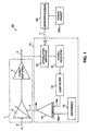
- FIGs. 1 and 2 when taken together as will be apparent below, show a block diagram of a wide dynamic range power amplifier embodying the present invention.
- Fig. 1 shows one example of a wide dynamic range power amplifier 50 which includes a power amplification circuit 1 and a feedback circuit 10 under control of a digital control means.
- the digital control means may include microprocessor 20 and power adjust input device 20a, but many other alternatives are known to those of ordinary skill in the art.
- the microprocessor could be replaced by a minicomputer, mainframe, or any other suitable kind of digital controller.
- the power adjust input device 20a may include such things as a keypad, touch screen, RF transmitter, or any other mechanism capable of instructing a digital controller to change the output power to a certain level, such as a firmware program which is executed upon "power up" of the transmitter.
- the power amplification circuit 1 shown in Fig. 1 includes an analog variable gain amplifier 5 preceding the power amplifier 7 for receiving an input signal on line 2, but alternatively, just the power amplifier 7 may be used.
- the power amplification circuit 1 serves to increase or decrease the power of an incoming signal on line 2 to an outgoing signal with an output power suitable for transmitting the signal over a communication medium, such as the electromagnetic frequency spectrum in the case of an RF signal.
- the outgoing signal is transmitted at the output power from the power amplifier 7 on line 3.
- the feedback circuit 10 functions to change the output power to any of the different, discrete power levels selected via the power adjust input device 20a.
- the feedback circuit includes a digital step attenuator 12 for attenuating the power of the outgoing signal in response to the digital control means, from a first attenuation level to a second attenuation level, by an amount corresponding to the change in output power needed for the selected output power.
- the attenuation of the digital step attenuator is increased by 5 dB by microprocessor 20, from a first attenuation level, for example 0 dB, to a second attenuation level of 5 dB, which is 5 dB higher.
- the output power at the second attenuation level namely 5 dBm (the present output power of 10 dBm minus the second attenuation level of 5 dB) is converted to a corresponding D.C. voltage by a power conversion circuit, such as the power detector 13 and loop filter 14 shown in Fig. 1.
- the power detector 13 and loop filter 14 serve to fully rectify and integrate the outgoing signal to output a D.C. voltage which corresponds to the output power of the outgoing signal at the second attenuation level.
- the power detector is suitably a diode detector, but alternative devices can be used as known to those of ordinary skill in the art.
- the loop filter is also just one example of a suitable integrating device.
- the 5 dBm D.C. voltage representing the output power at the second attenuation level, is compared by a comparator 16 to a reference D.C. voltage 15.
- the reference D.C. voltage is the D.C. voltage corresponding to the output power at the first attenuation level, which, in this example, is a D.C. voltage corresponding to 10 dBm (10 dBm output power minus the first attenuation level of 0 dB).
- the difference between the 5 dBm D.C. voltage at the feedback input 16a to the comparator and the 10 dBm reference D.C. voltage at the reference input 16b is 5 dBm.
- the comparator seeks to maintain equality between its two inputs, it will change the gain of the power amplification circuit 1 by an amount corresponding to the 5 dBm difference between its two inputs, which, in turn, will change the output power from 10 dBm to 15 dBm, the desired output power.
- the D.C. voltage output from the power detector corresponding to the new 15 dBm output power at the second attenuation level, will be a 10 dBm D.C. voltage, which equals the 10 dBm reference D.C. voltage.
- the comparator will not change the output power again because its two inputs are now equal.
- the comparator changes the gain of the analog variable gain amplifier 5 of the power amplification circuit.
- the gain of the power amplifier 7 could be changed instead.
- the output 16c of the comparator is operably coupled to the gain control input 4 of the power amplification circuit 1, which, in turn, is operably coupled to the gain control input of the analog variable gain amplifier 5.
- the present example changed the output power by 5 dB which is within the dynamic range of the typical power detector, meaning that the power detector will output a D.C. voltage which is proportional to the output power sensed at its input.
- the advantage of the present invention over the prior art devices discussed in the Background of the Invention occurs when the output power needs to be changed by more than the dynamic range of the power detector, which is typically on the order of 10 dB. In other words, one significant advantage of the present over the prior art devices discussed in the Background is in wide dynamic range applications.
- the user will first select 25 dBm as the new desired output power by way of the power adjust input device 20a.
- this new desired output power might be set by a signal from a base station or the like.
- the microprocessor 20 will increase the attenuation of the digital step attenuator by 15 dB, from 0 dB (the first attenuation level) to 15 dB (the second attenuation level).
- the 15 dB attenuation level will, in turn, decrease the output power sensed by the power detector from 10 dBm, the output power at the first attenuation level, to -5 dBm, the output power at the second attenuation level.
- the power detector and loop filter will not output a D.C. voltage which corresponds to -5 dBm. Instead, the D.C. voltage will correspond to only -3 dBm, because of the power detector's 2 dBm error.
- the comparator seeking to maintain equality between its two inputs, will only increase the gain of the power amplification circuit 1 by 13 dBm, the difference between the -3 dBm D.C. voltage and the 10 dBm reference voltage.
- the output power will increase from 10 dBm to a new output power of 23 dBm, which is 2 dBm less than the desired power level.
- the feedback circuit will continue to servo to correct the 2 dBm error because the new 23 dBm output power at the 15 dB second attenuation level is 8 dBm, which is within the 10 dB dynamic range of the power detector.
- 8 dBm represents only a 2 dB change from the 10 dBm output power sensed prior to the increase in attenuation. Because the change is within the dynamic range of the power detector, the power detector will output a D.C. voltage to the comparator which corresponds to 8 dBm.
- the comparator to maintain equality between its two inputs, will increase the gain of the power amplifier another 2 dBm, which, in turn, will increase the output power from 23 dBm to the desired output power of 25 dBm.
- the detector will now see 10 dBm (the 25 dBm output power minus the 15 dB second attenuation level) at its input and will output a 10 dBm voltage to the feedback input of the comparator. Because the two inputs to the comparator are now equal, the output power will remain at the desired 25 dBm level.
- the power amplifier described above is not limited by the dynamic range of the power detector, and unlike the prior art devices which compensate for the error, this power amplifier corrects the error.
- the problem associated with the power detector is solved without the complexity, cost, and decrease in reliability associated with the prior art solution of adjusting the reference voltage to compensate for the error.
- An alternative embodiment which is not claimed, could use a digital variable gain amplifier 12 as indicated in Fig. 1, in place of the digital step attenuator, at the input to the power detector for changing the output power.
- the output power is amplified, from a first amplification level to a second amplification level, by an amount - in dB - in opposite polarity to the change in the output power desired.
- the gain of the amplifier is decreased to increase the output power, and increased to decrease the output power.
- the D.C. voltage corresponds to the output power at the second amplification level
- the reference voltage corresponds to the output power at the first amplification.
- the comparator will increase the output power of the power amplifier by an amount corresponding to the difference between the D.C. voltage and the reference D.C. voltage until the D.C. voltage equals the reference D.C. voltage.
- the feedback circuit 10 changes the gain of the power amplification circuit 1 over a wide dynamic range
- the power amplification circuit must be sensitive to changes in the output of the comparator over the same wide dynamic range.
- the power amplification circuit 1 is also highly sensitive to spurious signals in the feedback signal over the wide dynamic range, which may leave it prone to unwanted AM modulation.
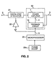
- Fig. 2 shows an arrangement which greatly reduces this sensitivity.
- a second digital step attenuator 21 is operably coupled to the input 2 of the power amplification circuit or power amplifier 1 and operates in a reciprocal manner with the first digital step attenuator 12 of the feedback circuit 10 shown in Fig. 1.
- the attenuation of the second digital step attenuator 21 is controlled by the same digital control means 20 as the first digital step attenuator 12, but through an inverter, enabling the second attenuator to be controlled in a reciprocal or opposite relationship with the first digital step attenuator.
- the attenuation of the first attenuator is increased, the attenuation of the second attenuator is simultaneously decreased by the same amount. In other words, the attenuation is changed by an amount (dB) in opposite polarity to the change in output power desired.
- the power amplification circuit 1 need only have a small dynamic range which accommodates changes resulting from changes in the operating environment, for example temperature changes. With a small dynamic range, the power amplification circuit will have a small sensitivity at its gain control input 4.
- the second digital step attenuator could be replaced by a digital variable gain amplifier, and the digital control means could directly control the variable gain amplifier, rather than through an inverter, to accomplish the same result.
- the gain of the second digital variable gain amplifier would be changed by an amount corresponding to the change in output power desired, rather than in opposite polarity thereto.
- the present invention is particularly suited for use as a general purpose transmitter in base-station and mobile radios, including F.M. base-station radios, CDMA base-station radios, GSM base-station radios, TDMA base-station radios, and microcellular base-station radios.
- F.M. base-station radios including F.M. base-station radios, CDMA base-station radios, GSM base-station radios, TDMA base-station radios, and microcellular base-station radios.
Description
- This invention relates to wide dynamic range power amplifiers, and to methods of changing the output power of a power amplifier.
- Power amplifiers are commonly used as general purpose transmitters for wireless base-stations and handsets. In these applications, the power amplifier serves to change the power of an incoming signal to an output power suitable for transmitting the signal over a communication medium, such as the electromagnetic frequency spectrum in the case of a modulated RF carrier.
- The power of a signal is directly proportional to the amplitude or voltage level of the signal (P = V2/R) and is typically expressed in dBm units, which represent the logarithmic power of the signal with respect to 1 mW, (P in dBm units = 20 log10(V/10-3)). The change in power of a power amplifier is expressed in decibel (dB) units, (P change in
dB units 20 log10(Vout/Vin)). For example, a +6 dB change in power represents a gain in power by a factor of 2; a +20 dB change in power represents a gain in power by a factor of 10; and a +40 dB change in power represents a gain in power by a factor of 20. Negative dB changes in power represent reductions in power by an inverse factor. For example, -6 dB, -20 dB, and -40 dB, represent reductions in power by factors of 1/2, 1/10, and 1/20, respectively. - To maintain a desired output power over time, the power of the outgoing signal is continuously monitored and adjusted by a feedback circuit operably coupled between the output and gain control input of the power amplifier. The feedback circuit increases or decreases the gain of the power amplifier, and thereby the power of the signal, by an amount corresponding to the change in power needed to correct for fluctuations in the output power. These fluctuations are normally caused by environmental changes, such as changes in temperature, or spurious changes in the power of the incoming signal.
- In more detail, the amplitude of the outgoing signal is first rectified and integrated by a power detector and loop filter in the feedback circuit to obtain a D.C. voltage which corresponds to the actual output power of the signal. The D.C. voltage is then compared by a comparator with a reference D.C. voltage which corresponds to the desired output power. The comparator outputs a D.C voltage to the gain control input of the power amplifier which corresponds to the difference between the output power D.C. voltage and the reference D.C. voltage. This feedback signal from the comparator serves to increase or decrease the gain of the power amplifier to correct fluctuations in the output power from its desired level, and thereby maintain the power of the outgoing signal at the desired power level.
- Beyond maintaining a desired output power over time, existing transmitter applications also require that the output power be changed to different, discrete levels over varying ranges in power. One way to change the output power is to change the reference D.C. voltage from one which corresponds to the present output power to one which corresponds to the new, desired output power. In this way, the difference between the D.C. voltage and the reference D.C. voltage will correspond to the increase or decrease in gain required to change the output power of the outgoing signal to the new desired output power.
- This method is problematic for transmitter applications having wide dynamic ranges because of the small dynamic range of the typical, off-the-shelf power detector, which is often on the order of 10dB. The dynamic range of a power amplifier or power detector is the maximum dB range in power which the amplifier or detector can operate over without unacceptable levels of error.
- In other words, because the voltage-current characteristic curve associated with the typical power detector is non-linear, the output power sensed by the power detector cannot change by more than 10 dB without unacceptable levels of error, whereby the power detector produces a D.C. voltage which does not correspond to the actual output power -- for example, it does not correspond to within 1 dbm as required by the IF-54 standard for base station transmitters. Transmitter applications, on the other hand, often require that the output power change by more than 10 dB, in other words, over a wide dynamic range.
- Briefly, by way of example, to change the output power from 10 dBm to 25 dBm, a 15 dB change, the reference D.C. voltage input to the comparator is changed from a 10 dBm voltage to a 25 dBm voltage. Assuming that the power detector has a 2 dBm error outside its 10 dB dynamic range, the power detector will only output a 23 dBm D.C. voltage to the feedback input of the comparator. To maintain equality between its two inputs, the comparator will increase the gain of the power amplifier and thus the output power by another 2 dBm, to 27 dBm, so that a 25 dBm D.C. voltage (the 27 dBm output power minus the 2 dBm error) is input to the comparator. This leaves the output of the power amplifier at the wrong power level of 27 dBm.
- One way to compensate for the error associated with the power detector outside its dynamic range is to adjust or calibrate the reference voltage. For the above example, the reference voltage would be adjusted or calibrated to a 23 dBm voltage, rather than a 25 dBm voltage, when a 25 dBm output power is desired. Since the error associated with the power detector is not fixed, in order to make these adjustments or calibrations for each of the different power levels over a wide dynamic range, a number of additional components must be added to the feedback circuit, increasing the complexity and cost of the power amplifier, and decreasing its reliability.
- EP-A-0509733 discloses a RF power amplifier which uses a variable attenuator or variable coupling network to attenuate the output power by an amount corresponding to the desired change in output power.
- US-A-5204637 discloses an RF power amplifier which uses a variable coupling network to control the amount of output power in wide dynamic range applications that is transferred to a power detector, so that the power level detected by the power detector is an indirect, linearly proportional change in power reflective of the actual change in output power, but at a power level within the narrow dynamic range of the power detector, i.e., the range within which the power detector will operate in a linear manner.
- According to one aspect of this invention there is provided a wide dynamic range power amplifier as claimed in
claim 1. - According to another aspect of this invention there is provided a method as claimed in
claim 2. - In an embodiment of the present invention, a power amplifier is provided which does not require calibrations or adjustments to the reference D.C. voltage to change the output power to different output power levels over a wide dynamic range. As a result, the number of components required to operate the power amplifier are greatly reduced, resulting in a less complex, lower cost, more reliable wide dynamic range power amplifier.
- This wide dynamic range power amplifier includes a power amplification circuit for transmitting a signal at an output power, and a feedback circuit which changes the output power by changing the corresponding D.C. voltage, not the reference D.C. voltage. To change the D.C. voltage, the feedback circuit may suitably include a digital step attenuator coupled to the input of a power detector for attenuating the output power sensed by the power detector, from a first attenuation level to a second attenuation level, by an amount corresponding to the change in output power desired.
- A power conversion circuit, including a power detector in combination with a loop filter or integrator, converts the output power at the second attenuation level to a corresponding D.C. voltage. The D.C. voltage is then compared by a comparator to a reference D.C. voltage corresponding to the output power at the first attenuation level.
- Next, the comparator changes the output power by an amount corresponding to the difference between the D.C. voltage and the reference D.C. voltage. If the new output power is not at the desired power level because of the error associated with the small dynamic range of the power detector, the comparator will continue to servo until the D.C. voltage equals the reference D.C. voltage, and, as a result, the output power is at the desired level. This is possible because the D.C. voltage corresponding to the new output power at the second attenuation level will represent a change at the input to the power detector which is within its dynamic range, as explained further in the Detailed Description of the Invention.
- In an alternative embodiment, which is not claimed, a digital variable gain amplifier is used in place of the digital step attenuator to amplify the output power, from a first amplification level to a second amplification level, by an amount corresponding in opposite polarity to the desired change in output power. In this embodiment, the comparison is between a D.C. voltage corresponding to the output power at the second amplification level, and a reference D.C. voltage corresponding to the output power at the first amplification level. Otherwise, the operation of the two embodiments is the same.
- Because the feedback circuit of the present invention operates over a wide dynamic range in power, the power amplification circuit preferably should also operate over the same wide dynamic range. But this may leave the gain control input of the power amplification circuit prone to AM modulation as a result of spurious changes in the difference signal from the comparator of the feedback circuit.
- In order to greatly reduce the sensitivity of the power amplification circuit by eliminating the need for the gain control input of the power amplification circuit to change over a wide dynamic range, and thereby allowing the power amplifier to use a power amplification circuit having a small dynamic range,
a second digital step attenuator is operably coupled to the input of the power amplification circuit for attenuating the input power, from a first attenuation level to a second attenuation level, by an amount -in dB- in opposite polarity to the change in output power desired. The attenuation of the input power to the second attenuation level occurs simultaneously with the attenuation of the output power to the second attenuation level. In this way, the input power is changed to the level of the desired output power, meaning that the gain of the power amplification circuit will only need to change to compensate for the small power changes associated with environmental changes. Thus, a power amplification circuit with a small dynamic range can be used with the present invention, eliminating its sensitivity to spurious signals over a wide dynamic range. - Other embodiments include replacing the second digital step attenuator with a digital variable gain amplifier which amplifies the input power by an amount corresponding to the change in output power desired.
- Figs. 1 and 2, when taken together as will be apparent below, show a block diagram of a wide dynamic range power amplifier embodying the present invention.
- Fig. 1 shows one example of a wide dynamic
range power amplifier 50 which includes apower amplification circuit 1 and afeedback circuit 10 under control of a digital control means. - The digital control means may include
microprocessor 20 and power adjustinput device 20a, but many other alternatives are known to those of ordinary skill in the art. For example, the microprocessor could be replaced by a minicomputer, mainframe, or any other suitable kind of digital controller. The power adjustinput device 20a may include such things as a keypad, touch screen, RF transmitter, or any other mechanism capable of instructing a digital controller to change the output power to a certain level, such as a firmware program which is executed upon "power up" of the transmitter. - The
power amplification circuit 1 shown in Fig. 1 includes an analogvariable gain amplifier 5 preceding thepower amplifier 7 for receiving an input signal online 2, but alternatively, just thepower amplifier 7 may be used. Thepower amplification circuit 1 serves to increase or decrease the power of an incoming signal online 2 to an outgoing signal with an output power suitable for transmitting the signal over a communication medium, such as the electromagnetic frequency spectrum in the case of an RF signal. The outgoing signal is transmitted at the output power from thepower amplifier 7 online 3. - The
feedback circuit 10 functions to change the output power to any of the different, discrete power levels selected via the power adjustinput device 20a. Specifically, the feedback circuit includes adigital step attenuator 12 for attenuating the power of the outgoing signal in response to the digital control means, from a first attenuation level to a second attenuation level, by an amount corresponding to the change in output power needed for the selected output power. For example, to change the output power from 10 dBm to 15 dBm, representing a change of 5 dB, the attenuation of the digital step attenuator is increased by 5 dB bymicroprocessor 20, from a first attenuation level, for example 0 dB, to a second attenuation level of 5 dB, which is 5 dB higher. - Continuing with this example to explain Fig. 1, the output power at the second attenuation level, namely 5 dBm (the present output power of 10 dBm minus the second attenuation level of 5 dB) is converted to a corresponding D.C. voltage by a power conversion circuit, such as the
power detector 13 andloop filter 14 shown in Fig. 1. Specifically, thepower detector 13 andloop filter 14 serve to fully rectify and integrate the outgoing signal to output a D.C. voltage which corresponds to the output power of the outgoing signal at the second attenuation level. The power detector is suitably a diode detector, but alternative devices can be used as known to those of ordinary skill in the art. The loop filter is also just one example of a suitable integrating device. - Next, the 5 dBm D.C. voltage, representing the output power at the second attenuation level, is compared by a
comparator 16 to areference D.C. voltage 15. The reference D.C. voltage is the D.C. voltage corresponding to the output power at the first attenuation level, which, in this example, is a D.C. voltage corresponding to 10 dBm (10 dBm output power minus the first attenuation level of 0 dB). The difference between the 5 dBm D.C. voltage at thefeedback input 16a to the comparator and the 10 dBm reference D.C. voltage at thereference input 16b is 5 dBm. - Because the comparator seeks to maintain equality between its two inputs, it will change the gain of the
power amplification circuit 1 by an amount corresponding to the 5 dBm difference between its two inputs, which, in turn, will change the output power from 10 dBm to 15 dBm, the desired output power. The D.C. voltage output from the power detector, corresponding to the new 15 dBm output power at the second attenuation level, will be a 10 dBm D.C. voltage, which equals the 10 dBm reference D.C. voltage. The comparator will not change the output power again because its two inputs are now equal. - In more detail, to change the output power, the comparator changes the gain of the analog
variable gain amplifier 5 of the power amplification circuit. In other applications, the gain of thepower amplifier 7 could be changed instead. As show in Fig. 1, theoutput 16c of the comparator is operably coupled to thegain control input 4 of thepower amplification circuit 1, which, in turn, is operably coupled to the gain control input of the analogvariable gain amplifier 5. - The present example changed the output power by 5 dB which is within the dynamic range of the typical power detector, meaning that the power detector will output a D.C. voltage which is proportional to the output power sensed at its input. The advantage of the present invention over the prior art devices discussed in the Background of the Invention occurs when the output power needs to be changed by more than the dynamic range of the power detector, which is typically on the order of 10 dB. In other words, one significant advantage of the present over the prior art devices discussed in the Background is in wide dynamic range applications.
- This advantage is illustrated by the following example. Assume that the dynamic range of the
power detector 13 is 10 dB. Also, assume that the output power has initially been set at 10 dBm, that the first attenuation level of thedigital step attenuator 12 is 0 dB, and that thereference D.C. voltage 15 is 10 dBm (the output power of 10 dBm minus the 0 dB first attenuation level). Finally, assume that the output power needs to be changed this time by 15 dB, from 10 dBm to 25 dBm, which is beyond the 10 dB dynamic range of the power detector, meaning that the power detector will output a D.C. voltage with an unacceptable level of error. Assume the error is 2 dBm. - With these assumptions, the user will first select 25 dBm as the new desired output power by way of the power adjust
input device 20a. Alternatively, this new desired output power might be set by a signal from a base station or the like. In response to that selection, themicroprocessor 20 will increase the attenuation of the digital step attenuator by 15 dB, from 0 dB (the first attenuation level) to 15 dB (the second attenuation level). The 15 dB attenuation level will, in turn, decrease the output power sensed by the power detector from 10 dBm, the output power at the first attenuation level, to -5 dBm, the output power at the second attenuation level. - Because the input to the power detector has changed by more than 10 dB, the power detector and loop filter will not output a D.C. voltage which corresponds to -5 dBm. Instead, the D.C. voltage will correspond to only -3 dBm, because of the power detector's 2 dBm error. The comparator, in turn, seeking to maintain equality between its two inputs, will only increase the gain of the
power amplification circuit 1 by 13 dBm, the difference between the -3 dBm D.C. voltage and the 10 dBm reference voltage. In response to the 13 dB increase in the gain of thepower amplification circuit 1, the output power will increase from 10 dBm to a new output power of 23 dBm, which is 2 dBm less than the desired power level. - Unlike the prior art devices discussed in the Background of the Invention, the feedback circuit will continue to servo to correct the 2 dBm error because the new 23 dBm output power at the 15 dB second attenuation level is 8 dBm, which is within the 10 dB dynamic range of the power detector. In other words, 8 dBm represents only a 2 dB change from the 10 dBm output power sensed prior to the increase in attenuation. Because the change is within the dynamic range of the power detector, the power detector will output a D.C. voltage to the comparator which corresponds to 8 dBm.
- The comparator, to maintain equality between its two inputs, will increase the gain of the power amplifier another 2 dBm, which, in turn, will increase the output power from 23 dBm to the desired output power of 25 dBm. The detector will now see 10 dBm (the 25 dBm output power minus the 15 dB second attenuation level) at its input and will output a 10 dBm voltage to the feedback input of the comparator. Because the two inputs to the comparator are now equal, the output power will remain at the desired 25 dBm level.
- Thus, the power amplifier described above is not limited by the dynamic range of the power detector, and unlike the prior art devices which compensate for the error, this power amplifier corrects the error. As a result, the problem associated with the power detector is solved without the complexity, cost, and decrease in reliability associated with the prior art solution of adjusting the reference voltage to compensate for the error.
- An alternative embodiment, which is not claimed, could use a digital
variable gain amplifier 12 as indicated in Fig. 1, in place of the digital step attenuator, at the input to the power detector for changing the output power. In the case of the digital variable gain amplifier, the output power is amplified, from a first amplification level to a second amplification level, by an amount - in dB - in opposite polarity to the change in the output power desired. In other words, the gain of the amplifier is decreased to increase the output power, and increased to decrease the output power. - In this embodiment, the D.C. voltage corresponds to the output power at the second amplification level, and the reference voltage corresponds to the output power at the first amplification. As in the first embodiment, the comparator will increase the output power of the power amplifier by an amount corresponding to the difference between the D.C. voltage and the reference D.C. voltage until the D.C. voltage equals the reference D.C. voltage.
- Because the
feedback circuit 10 as so far described changes the gain of thepower amplification circuit 1 over a wide dynamic range, the power amplification circuit must be sensitive to changes in the output of the comparator over the same wide dynamic range. As a result, thepower amplification circuit 1 is also highly sensitive to spurious signals in the feedback signal over the wide dynamic range, which may leave it prone to unwanted AM modulation. Fig. 2 shows an arrangement which greatly reduces this sensitivity. - Referring to Fig. 2, a second
digital step attenuator 21 is operably coupled to theinput 2 of the power amplification circuit orpower amplifier 1 and operates in a reciprocal manner with the firstdigital step attenuator 12 of thefeedback circuit 10 shown in Fig. 1. The attenuation of the seconddigital step attenuator 21 is controlled by the same digital control means 20 as the firstdigital step attenuator 12, but through an inverter, enabling the second attenuator to be controlled in a reciprocal or opposite relationship with the first digital step attenuator. In this way, when the attenuation of the first attenuator is increased, the attenuation of the second attenuator is simultaneously decreased by the same amount. In other words, the attenuation is changed by an amount (dB) in opposite polarity to the change in output power desired. - Less attenuation means the input power will increase, and if the increase in attenuation is in opposite polarity to the amount of change in output power desired, the input power will rise to the level of the desired output power. Thus, the
power amplification circuit 1 need only have a small dynamic range which accommodates changes resulting from changes in the operating environment, for example temperature changes. With a small dynamic range, the power amplification circuit will have a small sensitivity at itsgain control input 4. - There are other suitable alternatives for the arrangement shown in Fig. 2. For example, the second digital step attenuator could be replaced by a digital variable gain amplifier, and the digital control means could directly control the variable gain amplifier, rather than through an inverter, to accomplish the same result. The gain of the second digital variable gain amplifier would be changed by an amount corresponding to the change in output power desired, rather than in opposite polarity thereto.
- The present invention is particularly suited for use as a general purpose transmitter in base-station and mobile radios, including F.M. base-station radios, CDMA base-station radios, GSM base-station radios, TDMA base-station radios, and microcellular base-station radios.
- Other embodiments and applications for the present invention will be readily apparent to those of ordinary skill in the art, and all such embodiments and applications for the present invention are considered to fall within the scope of the invention as defined by the appended claims.
Claims (2)
- A wide dynamic range amplifier (50) comprising a power amplification circuit (1) having an input, an output (3), and a gain control, characterized by:a first digital step attenuator (12) having an input coupled to the output of the power amplification circuit, and an output coupled to a power conversion circuit, (13, 14), wherein the power conversion circuit converts power at the output of the power amplification circuit to a corresponding D.C.voltage, following attenuation by the first digital step attenuator;a second digital step attenuator (21) having an input, and an output coupled to the input of the power amplification circuit;a controller (20) coupled to control inputs of the first and second digital step attenuators, and programmed for attenuating the first digital step attenuator by an amount corresponding to a desired change in output power at the output to the power amplification circuit, and simultaneously attenuating the second digital step attenuator by the same amount but in opposite relationship to the amount corresponding to the desired change in output power; anda comparator (16) having a first input coupled to the D.C. voltage output (16a) from the power conversion circuit, a second input coupled to a reference D.C. voltage (16b), and an output (16c) coupled to the gain control (4) of the power amplification circuit, wherein a D.C. voltage representative of a difference between the first and second inputs is output from the comparator to the gain control input of the power amplification circuit.
- A method of changing the output power of a power amplifier(50),comprising the steps of:generating an output power from a power amplifier (1) having an input power;attenuating, under the control of a controller (20), the output power by an amount corresponding to a desired change in the output power;attenuating, under the control of said controller (20), the input power by the same amount but in opposite relationship to the desired change in the output power, said attenuation of the input power occurring simultaneously with the attenuation of the output power;converting the attenuated output power to a corresponding D.C. voltage;generating a reference D.C. voltage corresponding to a reference output power;comparing the D.C. voltage to the reference D.C. voltage; andchanging the output power by an amount corresponding to the difference between the D.C. voltage and the reference D.C. voltage.
Applications Claiming Priority (2)
| Application Number | Priority Date | Filing Date | Title |
|---|---|---|---|
| US36608194A | 1994-12-29 | 1994-12-29 | |
| US366081 | 1994-12-29 |
Publications (3)
| Publication Number | Publication Date |
|---|---|
| EP0720287A2 EP0720287A2 (en) | 1996-07-03 |
| EP0720287A3 EP0720287A3 (en) | 1997-10-15 |
| EP0720287B1 true EP0720287B1 (en) | 2003-01-15 |
Family
ID=23441593
Family Applications (1)
| Application Number | Title | Priority Date | Filing Date |
|---|---|---|---|
| EP95309095A Expired - Lifetime EP0720287B1 (en) | 1994-12-29 | 1995-12-13 | Wide dynamic range power amplifier |
Country Status (3)
| Country | Link |
|---|---|
| US (1) | US5646578A (en) |
| EP (1) | EP0720287B1 (en) |
| DE (1) | DE69529395T2 (en) |
Families Citing this family (29)
| Publication number | Priority date | Publication date | Assignee | Title |
|---|---|---|---|---|
| JPH08307182A (en) * | 1995-04-27 | 1996-11-22 | Sony Corp | Power control circuit |
| JPH0918358A (en) * | 1995-06-27 | 1997-01-17 | Sony Corp | Radio transmitter |
| SE506842C2 (en) * | 1996-06-28 | 1998-02-16 | Ericsson Telefon Ab L M | Device and method of radio transmitters for control of power amplifiers |
| US5751190A (en) * | 1996-08-22 | 1998-05-12 | Northern Telecom Limited | Gain-controlled amplifier and distributed amplifier |
| KR100193842B1 (en) * | 1996-09-13 | 1999-06-15 | 윤종용 | Power Control Circuit and Method of Wireless Communication System |
| JP2856250B2 (en) * | 1997-06-27 | 1999-02-10 | 日本電気株式会社 | Amplifier gain compensator for code multiplex communication system |
| US6148048A (en) * | 1997-09-26 | 2000-11-14 | Cirrus Logic, Inc. | Receive path implementation for an intermediate frequency transceiver |
| US6917245B2 (en) * | 2000-09-12 | 2005-07-12 | Silicon Laboratories, Inc. | Absolute power detector |
| US6549071B1 (en) * | 2000-09-12 | 2003-04-15 | Silicon Laboratories, Inc. | Power amplifier circuitry and method using an inductance coupled to power amplifier switching devices |
| US6828859B2 (en) * | 2001-08-17 | 2004-12-07 | Silicon Laboratories, Inc. | Method and apparatus for protecting devices in an RF power amplifier |
| GB0210168D0 (en) * | 2002-05-03 | 2002-06-12 | Zarlink Semiconductor Ltd | Signal processing stage and radio frequency tuner |
| US6894565B1 (en) * | 2002-12-03 | 2005-05-17 | Silicon Laboratories, Inc. | Fast settling power amplifier regulator |
| US6897730B2 (en) * | 2003-03-04 | 2005-05-24 | Silicon Laboratories Inc. | Method and apparatus for controlling the output power of a power amplifier |
| US7171171B1 (en) * | 2003-08-15 | 2007-01-30 | Rf Micro Devices, Inc. | GaAs RF signal detection circuit with operational amplifier |
| US7023278B1 (en) * | 2004-09-21 | 2006-04-04 | Rockwell Collins, Inc. | Digital power amplifier level control |
| KR100656333B1 (en) * | 2005-04-27 | 2006-12-13 | 한국과학기술원 | Power amplifier with automatically switching facility |
| US8559896B2 (en) * | 2005-06-30 | 2013-10-15 | Harris Stratex Networks, Inc. | System and method for radio power level control |
| CN101295965B (en) * | 2007-04-27 | 2010-05-26 | 北京朗波芯微技术有限公司 | Digital automatic gain control circuit apparatus |
| CN101908902A (en) * | 2009-06-08 | 2010-12-08 | 深圳富泰宏精密工业有限公司 | Wireless communication device and power amplification efficiency control module thereof |
| US8536949B1 (en) * | 2009-10-22 | 2013-09-17 | Sprint Communications Company L.P. | Variable power amplifier system |
| DE112010005225T5 (en) * | 2010-02-04 | 2012-11-15 | Epcos Ag | Amplifier circuit and method for signal detection |
| US8604777B2 (en) * | 2011-07-13 | 2013-12-10 | Allegro Microsystems, Llc | Current sensor with calibration for a current divider configuration |
| US9413320B1 (en) * | 2013-10-25 | 2016-08-09 | Anadigics, Inc. | Programmable broad bandwidth gain amplifier |
| EP2869465B1 (en) * | 2013-11-01 | 2016-05-25 | Nxp B.V. | RF amplifier |
| US9825657B2 (en) * | 2016-01-12 | 2017-11-21 | Google Inc. | Digital pre-distortion linearization for mobile communication |
| US10164593B1 (en) * | 2017-09-07 | 2018-12-25 | Silicon Laboratories Inc. | Accurate, low-power power detector circuits and related methods using programmable reference circuitry |
| US10063203B1 (en) * | 2017-09-07 | 2018-08-28 | Silicon Laboratories Inc. | Accurate, low-power power detector circuits and related methods |
| US11394471B1 (en) * | 2021-03-24 | 2022-07-19 | The United States Of America As Represented By The Secretary Of The Army | High-power radio frequency (RF) power detector |
| CN114337601B (en) * | 2022-03-15 | 2022-05-24 | 深圳市鼎阳科技股份有限公司 | Ultra-wideband microwave signal generator |
Family Cites Families (4)
| Publication number | Priority date | Publication date | Assignee | Title |
|---|---|---|---|---|
| JPS61210728A (en) * | 1985-03-14 | 1986-09-18 | Alps Electric Co Ltd | Output power control device for transmitter |
| JP2871889B2 (en) * | 1991-04-16 | 1999-03-17 | 三菱電機株式会社 | High frequency power amplifier |
| US5150075A (en) * | 1991-06-03 | 1992-09-22 | Motorola, Inc. | Power amplifier ramp up method and apparatus |
| US5204637A (en) * | 1992-04-17 | 1993-04-20 | Hughes Aircraft Company | Power detection technique for automatic amplifier power control |
-
1995
- 1995-12-13 EP EP95309095A patent/EP0720287B1/en not_active Expired - Lifetime
- 1995-12-13 DE DE69529395T patent/DE69529395T2/en not_active Expired - Lifetime
-
1996
- 1996-07-30 US US08/688,415 patent/US5646578A/en not_active Expired - Lifetime
Also Published As
| Publication number | Publication date |
|---|---|
| DE69529395D1 (en) | 2003-02-20 |
| EP0720287A2 (en) | 1996-07-03 |
| US5646578A (en) | 1997-07-08 |
| EP0720287A3 (en) | 1997-10-15 |
| DE69529395T2 (en) | 2003-11-20 |
Similar Documents
| Publication | Publication Date | Title |
|---|---|---|
| EP0720287B1 (en) | Wide dynamic range power amplifier | |
| US4602218A (en) | Automatic output control circuitry for RF power amplifiers with wide dynamic range | |
| US5307512A (en) | Power control circuitry for achieving wide dynamic range in a transmitter | |
| RU2297714C2 (en) | System and mode for calibration of control over the power of a radio communication arrangement | |
| RU2134018C1 (en) | Method and device for correction and limiting of reversible radio communication and transmission power in radio telephone system | |
| RU2158474C2 (en) | Linearized digital automatic gain control | |
| CA2088813C (en) | Automatic level control circuit for dual mode analog/digital cellular telephone | |
| US6166598A (en) | Power amplifying circuit with supply adjust to control adjacent and alternate channel power | |
| US5107225A (en) | High dynamic range closed loop automatic gain control circuit | |
| WO1994029954A1 (en) | Temperature-compensated gain-controlled amplifier having a wide linear dynamic range | |
| WO2007008873A2 (en) | Polar loop radio frequency (rf) transmitter having increased dynamic range amplitude control | |
| EP0532203B1 (en) | Power controller | |
| JPH0449298B2 (en) | ||
| CN1224281A (en) | RF transmitter having temperature compensated output power level control circuit and method therefor | |
| JPH09186538A (en) | Wide dynamic range power amplifier | |
| EP2073383B1 (en) | Amplifier arrangement | |
| EP1145454B1 (en) | Apparatus and method for compensating rf gain based on measured rf noise | |
| JPH06152288A (en) | Power controller | |
| EP1523101A2 (en) | Radio transmitter | |
| KR20060032287A (en) | Apparatus and method for compensating rf transmission power in the mobile communication terminal | |
| KR100282398B1 (en) | Base station transmitter | |
| JP2855652B2 (en) | Transmission device | |
| JPH0481898B2 (en) | ||
| JPH09199960A (en) | Power amplifier | |
| JPH06104777A (en) | Signal amplifier |
Legal Events
| Date | Code | Title | Description |
|---|---|---|---|
| PUAI | Public reference made under article 153(3) epc to a published international application that has entered the european phase |
Free format text: ORIGINAL CODE: 0009012 |
|
| AK | Designated contracting states |
Kind code of ref document: A2 Designated state(s): DE GB SE |
|
| PUAL | Search report despatched |
Free format text: ORIGINAL CODE: 0009013 |
|
| AK | Designated contracting states |
Kind code of ref document: A3 Designated state(s): DE GB SE |
|
| 17P | Request for examination filed |
Effective date: 19980403 |
|
| 17Q | First examination report despatched |
Effective date: 20000405 |
|
| GRAH | Despatch of communication of intention to grant a patent |
Free format text: ORIGINAL CODE: EPIDOS IGRA |
|
| GRAH | Despatch of communication of intention to grant a patent |
Free format text: ORIGINAL CODE: EPIDOS IGRA |
|
| GRAA | (expected) grant |
Free format text: ORIGINAL CODE: 0009210 |
|
| AK | Designated contracting states |
Kind code of ref document: B1 Designated state(s): DE GB SE |
|
| REG | Reference to a national code |
Ref country code: GB Ref legal event code: FG4D |
|
| REF | Corresponds to: |
Ref document number: 69529395 Country of ref document: DE Date of ref document: 20030220 Kind code of ref document: P |
|
| REG | Reference to a national code |
Ref country code: SE Ref legal event code: TRGR |
|
| PLBE | No opposition filed within time limit |
Free format text: ORIGINAL CODE: 0009261 |
|
| STAA | Information on the status of an ep patent application or granted ep patent |
Free format text: STATUS: NO OPPOSITION FILED WITHIN TIME LIMIT |
|
| 26N | No opposition filed |
Effective date: 20031016 |
|
| PGFP | Annual fee paid to national office [announced via postgrant information from national office to epo] |
Ref country code: SE Payment date: 20101214 Year of fee payment: 16 |
|
| REG | Reference to a national code |
Ref country code: SE Ref legal event code: EUG |
|
| PG25 | Lapsed in a contracting state [announced via postgrant information from national office to epo] |
Ref country code: SE Free format text: LAPSE BECAUSE OF NON-PAYMENT OF DUE FEES Effective date: 20111214 |
|
| PGFP | Annual fee paid to national office [announced via postgrant information from national office to epo] |
Ref country code: GB Payment date: 20131219 Year of fee payment: 19 Ref country code: DE Payment date: 20131220 Year of fee payment: 19 |
|
| REG | Reference to a national code |
Ref country code: DE Ref legal event code: R119 Ref document number: 69529395 Country of ref document: DE |
|
| GBPC | Gb: european patent ceased through non-payment of renewal fee |
Effective date: 20141213 |
|
| PG25 | Lapsed in a contracting state [announced via postgrant information from national office to epo] |
Ref country code: DE Free format text: LAPSE BECAUSE OF NON-PAYMENT OF DUE FEES Effective date: 20150701 Ref country code: GB Free format text: LAPSE BECAUSE OF NON-PAYMENT OF DUE FEES Effective date: 20141213 |