EP0723302A2 - Photo-receiving device, and method of fabricating a photo-device - Google Patents
Photo-receiving device, and method of fabricating a photo-device Download PDFInfo
- Publication number
- EP0723302A2 EP0723302A2 EP96300405A EP96300405A EP0723302A2 EP 0723302 A2 EP0723302 A2 EP 0723302A2 EP 96300405 A EP96300405 A EP 96300405A EP 96300405 A EP96300405 A EP 96300405A EP 0723302 A2 EP0723302 A2 EP 0723302A2
- Authority
- EP
- European Patent Office
- Prior art keywords
- photo
- light
- electrodes
- receiving device
- optical guide
- Prior art date
- Legal status (The legal status is an assumption and is not a legal conclusion. Google has not performed a legal analysis and makes no representation as to the accuracy of the status listed.)
- Granted
Links
- 238000004519 manufacturing process Methods 0.000 title claims description 26
- 230000003287 optical effect Effects 0.000 claims abstract description 111
- 239000000758 substrate Substances 0.000 claims abstract description 62
- 238000000034 method Methods 0.000 claims description 38
- 238000009413 insulation Methods 0.000 claims description 32
- 239000004065 semiconductor Substances 0.000 claims description 23
- 230000001681 protective effect Effects 0.000 claims description 20
- 230000008569 process Effects 0.000 claims description 18
- 239000000523 sample Substances 0.000 claims description 18
- 238000006243 chemical reaction Methods 0.000 claims description 13
- 239000000463 material Substances 0.000 claims description 13
- 229910052751 metal Inorganic materials 0.000 claims description 8
- 239000002184 metal Substances 0.000 claims description 8
- 239000012212 insulator Substances 0.000 claims description 6
- 230000003647 oxidation Effects 0.000 claims description 5
- 238000007254 oxidation reaction Methods 0.000 claims description 5
- 239000003362 semiconductor superlattice Substances 0.000 claims description 4
- 229910045601 alloy Inorganic materials 0.000 claims description 3
- 239000000956 alloy Substances 0.000 claims description 3
- 230000001747 exhibiting effect Effects 0.000 claims description 2
- 230000009466 transformation Effects 0.000 claims 1
- 239000010410 layer Substances 0.000 description 31
- 239000010408 film Substances 0.000 description 17
- 230000001965 increasing effect Effects 0.000 description 12
- 230000005684 electric field Effects 0.000 description 9
- 239000010936 titanium Substances 0.000 description 8
- 229910001218 Gallium arsenide Inorganic materials 0.000 description 7
- 238000005516 engineering process Methods 0.000 description 7
- 230000035945 sensitivity Effects 0.000 description 7
- RTAQQCXQSZGOHL-UHFFFAOYSA-N Titanium Chemical compound [Ti] RTAQQCXQSZGOHL-UHFFFAOYSA-N 0.000 description 6
- 239000000969 carrier Substances 0.000 description 6
- 230000015556 catabolic process Effects 0.000 description 6
- 238000005070 sampling Methods 0.000 description 6
- 229910052719 titanium Inorganic materials 0.000 description 6
- 239000011241 protective layer Substances 0.000 description 5
- 238000005215 recombination Methods 0.000 description 5
- 230000006798 recombination Effects 0.000 description 5
- GWEVSGVZZGPLCZ-UHFFFAOYSA-N Titan oxide Chemical compound O=[Ti]=O GWEVSGVZZGPLCZ-UHFFFAOYSA-N 0.000 description 4
- 238000010521 absorption reaction Methods 0.000 description 4
- 238000000609 electron-beam lithography Methods 0.000 description 4
- 238000005259 measurement Methods 0.000 description 4
- 230000010287 polarization Effects 0.000 description 4
- OGIDPMRJRNCKJF-UHFFFAOYSA-N titanium oxide Inorganic materials [Ti]=O OGIDPMRJRNCKJF-UHFFFAOYSA-N 0.000 description 4
- 230000015572 biosynthetic process Effects 0.000 description 3
- 239000013078 crystal Substances 0.000 description 3
- 230000000694 effects Effects 0.000 description 3
- 239000012774 insulation material Substances 0.000 description 3
- 238000007740 vapor deposition Methods 0.000 description 3
- 238000001514 detection method Methods 0.000 description 2
- 238000012986 modification Methods 0.000 description 2
- 230000004048 modification Effects 0.000 description 2
- 238000004544 sputter deposition Methods 0.000 description 2
- 239000010409 thin film Substances 0.000 description 2
- 230000005641 tunneling Effects 0.000 description 2
- 229910000980 Aluminium gallium arsenide Inorganic materials 0.000 description 1
- 229910000530 Gallium indium arsenide Inorganic materials 0.000 description 1
- 229910000673 Indium arsenide Inorganic materials 0.000 description 1
- 229910012463 LiTaO3 Inorganic materials 0.000 description 1
- 230000010748 Photoabsorption Effects 0.000 description 1
- 229910052581 Si3N4 Inorganic materials 0.000 description 1
- VYPSYNLAJGMNEJ-UHFFFAOYSA-N Silicium dioxide Chemical compound O=[Si]=O VYPSYNLAJGMNEJ-UHFFFAOYSA-N 0.000 description 1
- 230000005699 Stark effect Effects 0.000 description 1
- 239000006096 absorbing agent Substances 0.000 description 1
- 239000011358 absorbing material Substances 0.000 description 1
- XKRFYHLGVUSROY-UHFFFAOYSA-N argon Substances [Ar] XKRFYHLGVUSROY-UHFFFAOYSA-N 0.000 description 1
- 229910052786 argon Inorganic materials 0.000 description 1
- -1 argon ion Chemical class 0.000 description 1
- 239000011248 coating agent Substances 0.000 description 1
- 238000000576 coating method Methods 0.000 description 1
- 238000007796 conventional method Methods 0.000 description 1
- 230000003247 decreasing effect Effects 0.000 description 1
- 238000000151 deposition Methods 0.000 description 1
- 230000008021 deposition Effects 0.000 description 1
- 238000010586 diagram Methods 0.000 description 1
- 238000010292 electrical insulation Methods 0.000 description 1
- 230000002708 enhancing effect Effects 0.000 description 1
- 239000012535 impurity Substances 0.000 description 1
- RPQDHPTXJYYUPQ-UHFFFAOYSA-N indium arsenide Chemical compound [In]#[As] RPQDHPTXJYYUPQ-UHFFFAOYSA-N 0.000 description 1
- 230000010365 information processing Effects 0.000 description 1
- 239000011810 insulating material Substances 0.000 description 1
- 230000001590 oxidative effect Effects 0.000 description 1
- 238000000059 patterning Methods 0.000 description 1
- 230000035699 permeability Effects 0.000 description 1
- 238000003672 processing method Methods 0.000 description 1
- 238000009877 rendering Methods 0.000 description 1
- 230000004044 response Effects 0.000 description 1
- 238000000926 separation method Methods 0.000 description 1
- 229910052710 silicon Inorganic materials 0.000 description 1
- 239000010703 silicon Substances 0.000 description 1
- HQVNEWCFYHHQES-UHFFFAOYSA-N silicon nitride Chemical compound N12[Si]34N5[Si]62N3[Si]51N64 HQVNEWCFYHHQES-UHFFFAOYSA-N 0.000 description 1
- 229910052814 silicon oxide Inorganic materials 0.000 description 1
- 239000007787 solid Substances 0.000 description 1
- 238000001228 spectrum Methods 0.000 description 1
- 239000000126 substance Substances 0.000 description 1
Images


Classifications
-
- H—ELECTRICITY
- H01—ELECTRIC ELEMENTS
- H01L—SEMICONDUCTOR DEVICES NOT COVERED BY CLASS H10
- H01L31/00—Semiconductor devices sensitive to infrared radiation, light, electromagnetic radiation of shorter wavelength or corpuscular radiation and specially adapted either for the conversion of the energy of such radiation into electrical energy or for the control of electrical energy by such radiation; Processes or apparatus specially adapted for the manufacture or treatment thereof or of parts thereof; Details thereof
- H01L31/08—Semiconductor devices sensitive to infrared radiation, light, electromagnetic radiation of shorter wavelength or corpuscular radiation and specially adapted either for the conversion of the energy of such radiation into electrical energy or for the control of electrical energy by such radiation; Processes or apparatus specially adapted for the manufacture or treatment thereof or of parts thereof; Details thereof in which radiation controls flow of current through the device, e.g. photoresistors
- H01L31/10—Semiconductor devices sensitive to infrared radiation, light, electromagnetic radiation of shorter wavelength or corpuscular radiation and specially adapted either for the conversion of the energy of such radiation into electrical energy or for the control of electrical energy by such radiation; Processes or apparatus specially adapted for the manufacture or treatment thereof or of parts thereof; Details thereof in which radiation controls flow of current through the device, e.g. photoresistors characterised by at least one potential-jump barrier or surface barrier, e.g. phototransistors
- H01L31/101—Devices sensitive to infrared, visible or ultraviolet radiation
- H01L31/102—Devices sensitive to infrared, visible or ultraviolet radiation characterised by only one potential barrier or surface barrier
- H01L31/108—Devices sensitive to infrared, visible or ultraviolet radiation characterised by only one potential barrier or surface barrier the potential barrier being of the Schottky type
-
- H—ELECTRICITY
- H01—ELECTRIC ELEMENTS
- H01L—SEMICONDUCTOR DEVICES NOT COVERED BY CLASS H10
- H01L31/00—Semiconductor devices sensitive to infrared radiation, light, electromagnetic radiation of shorter wavelength or corpuscular radiation and specially adapted either for the conversion of the energy of such radiation into electrical energy or for the control of electrical energy by such radiation; Processes or apparatus specially adapted for the manufacture or treatment thereof or of parts thereof; Details thereof
- H01L31/02—Details
- H01L31/0232—Optical elements or arrangements associated with the device
- H01L31/02327—Optical elements or arrangements associated with the device the optical elements being integrated or being directly associated to the device, e.g. back reflectors
Definitions
- the present invention relates to an improved photo-receiving device for converting light signals to electrical signals, as required in such fields as communications and information processing, and to an improved method of fabricating a photo-device, which also means a light emitting device for converting electrical signals to light signals.
- photoelectric conversion refers to the function of converting a light signal to an electrical signal in a photo-receiving device, and also to the function of converting an electrical signal to a light signal in a light emitting device.
- Figure 8 illustrates the structure of a conventional photo-receiving device 50 as described in the IEEE Journal of Quantum Electronics (Vol. 28, pp. 2358-2368, 1992) for converting light signals to electrical signals at a relatively high speed.
- the photo-receiving device 50 comprises a substrate 11 that constitutes the photoelectric conversion portion (which can also be referred to as a light-absorbing portion, as this is a photo-receiving device), and a pair of opposed electrode portions 51, each in the form of a thin film of metal, formed on the surface of the substrate 11.
- the exposed surface of the substrate 11 between the electrodes 51 forms an optical window 13 for the entry of the light I P to be detected.
- excited carriers (electrons and holes) are generated in the substrate 11. Holes, shown in the drawing as blank circles, are drawn to the electrode 51 with the relatively negative (-) potential, and electrons, shown as solid circles, are drawn to the electrode 51 with the relatively positive (+) potential, setting up a flow of a photoelectric current (photo detection current) which takes place via the electrodes 51, whereby the incidence of the light I P is detected.
- photoelectric current photo detection current
- the width W of the optical window 13 that is, the smaller the distance between the electrodes 51, the faster the operating speed of the device is, and raising the applied voltage increases device speed and sensitivity. Also, making the width W of the optical window 13 no larger than the wavelength of the light I P to be detected imparts an evanescent field to the light I P impinging on the light-absorbing substrate 11 and causes the incident light I P to be absorbed in the vicinity of the surface of the substrate 11.
- MSM metal/semiconductor/metal
- the excited carriers generated in the vicinity of the surface of the substrate 11 are drawn rapidly to the electrodes 51, enabling higher speed operation to be achieved and the affect of carrier recombination to be reduced.
- a first problem is that, since the optical window 13 on the surface of the substrate 11 between the electrodes 51 is exposed, applying a higher voltage across the electrodes 51 giving rise to creeping discharge along the exposed surface of the optical window 13 and air-gap discharge, rendering the device unusable. That is, if the width W between the electrodes 51 is reduced beyond a certain limit, even a low voltage causes a dielectric breakdown. On the other hand, even in cases where the width W of the incident light window 13 can be increased, within the limitation that it does not exceed the wavelength of the incident light I P , there are major constraints on the voltage that can be applied.
- a second problem is that of the limits of the process technology. Even with existing electron beam lithography, a relatively high precision fine pattern process technology, an electrode gap cannot really be precision-fabricated to a width W of 100 nm or less, and even 300 nm or less is quite difficult.
- a conventional method of resolving the first problem is to cover, or bury, the exposed surface portion constituting the optical window 13 between the electrodes 51.
- This will now be described, with reference to Figure 9.
- the following description is not limited to photo-receiving devices, being also applicable to devices, such as light emitting devices, having a light emitting area defined in the form of an optical window.
- reference numeral 52 is used to denote the photo-device shown in Figure 9, the light-absorbing portion 11 of Figure 8 is the photoelectric conversion portion in the general meaning of the term, and the term metallic film electrodes 51 is encompassed by the term optically nontransparent conductive film (electrodes) 12.
- To fabricate the photo-device 52 existing lithographic technology is used to remove a prescribed region of an optically nontransparent conductive film 12 formed on photoelectric conversion portion 11, thereby exposing a defined portion that forms an optical window 13.
- Non-uniformities in the thickness of the surface deposition film gives rise to variation in device characteristics, and high frequency characteristics can be degraded by dielectric deposits.
- a very fine optical window is used, forming a high-quality insulative film over the window that has high dielectric resistance is difficult.
- An object of the present invention is to provide a high speed photo-receiving device in which constraints relating to the width W of the optical window between electrodes, and to the applied voltage, are reduced.
- Another object of the present invention is to provide a photo-receiving device that is more highly functional and multifunctional than conventional photo-receiving devices.
- Yet another object of the present invention is to provide a method of fabricating a photo-device wherein an optical window region and a protective layer over the optical window surface can be formed in one step.
- a further object of the present invention is to provide a method of fabricating a photo-device that enables the above-described drawbacks to be resolved or alleviated and an optical window to be formed to have a smaller width than that of conventional photo-devices.
- a photo-receiving device comprising a light-absorbing substrate, a pair of electrodes disposed on a surface of the light-absorbing substrate, an optical window through which light to be detected enters, said optical window being an exposed surface portion of the substrate between the electrodes, and an optical guide structure provided on the exposed surface portion of the substrate between the electrodes, said optical guide being permeable to the light to be detected, having a width that does not exceed a wavelength of the light to be detected, and exhibiting a higher resistance than that of the substrate.
- the electrodes can be brought closer together than in a conventional configuration without risk of dielectric breakdown between the electrodes.
- the optical guide also serves as a protective layer over the exposed surface portion of the substrate that constitutes the optical window. This eliminates the need to separately form a protective layer, thereby simplifying the fabrication process and reducing fabrication cost.
- the optical guide is formed of an insulating material.
- the insulator may be an oxide of the thin film material used to constitute the electrodes.
- the optical guide may be formed of a semiconductor material, provided the semiconductor material exhibits higher resistance than the light-absorbing substrate.
- the optical guide may be formed of materials having different properties.
- a photo-receiving device in which optical guide properties such as refractive index, absorption coefficient, polarization direction and the like can be varied.
- control electrodes can be included to apply voltage for effecting the adjustment of the optical properties of the optical guide.
- At least one of the control electrodes may be constituted by one of the above-described pair of electrodes.
- a semiconductor superlattice structure or Fabry-Perot resonator are representative examples of the type of arrangement that may be used to vary the optical properties of the optical guide.
- the insulation creepage distance between the electrodes is increased by making the thickness of the optical guide greater than the thickness of the electrodes.
- the photo-receiving device has a plurality of optical guides arranged in parallel between the pair of electrodes, and means each provided between adjacent optical guides so as not to transmit the light to be detected.
- a method of fabricating a photo-device comprising a step of forming an optically nontransparent, electrically conductive layer on a surface of a photoelectric conversion substrate, and a step whereby a portion of the optically nontransparent, electrically conductive layer is transformed to form over the optical window a light-permeable protective insulation structure of a prescribed width and length, and at the same time define an optical window region on the substrate surface beneath the protective insulation structure.
- the optically nontransparent, electrically conductive layer may be of a metal or an alloy, or a semiconductor (including semi-insulators), or may include a semiconductor superlattice structure.
- a photo-device is fabricated to have a prescribed area on a surface of the photo-receiving or photoemitting photoelectric conversion substrate forming an optical window of a prescribed width via which light is received or emitted.
- it is a photo-device that requires that an optically nontransparent, electrically conductive layer be formed at each side of the optical window, the defined optical window region and an insulation structure for protecting the optical window can be formed in a single step. This is highly efficient and eliminates the need to use a costly vacuum vapor deposition apparatus to form the protective layer over the entire surface.
- the optically nontransparent, electrically conductive layer is transformed by oxidation.
- This oxidation can be effected using a scanning probe apparatus.
- a fine optical window having a width that does not exceed the wavelength of the light to be detected, and a high-quality, highly dielectrically-resistant protective insulative structure for the optical window can both be formed by the same step.
- carrier speed is increased by applying a high field strength while the effect of carrier recombination is decreased, thus providing a photo-device that is faster and more sensitive.
- the photoelectric conversion substrate is of a light-absorbing material having a light receiving function, a non-transformed portion of the optically nontransparent, electrically conductive layer functions as an electrode to apply a voltage to the light-absorbing substrate, and the protective insulation structure functions as an optical guide that directs light to the substrate.
- the thickness of the protective insulation structure preferably is thicker than the thickness of the non-transformed portions of the optically nontransparent, electrically conductive layer at each side, and when said portions of the layer remaining at each side are utilized as a pair of electrodes, the insulation creepage distance between the electrodes is increased, thereby increasing the resistance to dielectric breakdown.
- Figure 1 shows an example of basic steps or processes used to fabricate a photo-device according to the method of the invention.
- parts corresponding to parts in the conventional devices 50 and 52 of Figures 8 and 9, already described, are given the same reference numerals.
- Figure 1 (A) shows a conductive, optically nontransparent film layer 12 formed on a surface of a light receiving or light emitting photoelectric conversion substrate 11.
- the internal constitution of the substrate 11 is not specifically defined by the invention, and may be comprised in accordance with existing device structural principles. If the device is formed as a conventional MSM photo-receiving device, as described in the foregoing, the substrate 11 will function as a light-absorber, and in terms of material, will be formed of a bulk semiconductor such as GaAs.
- the film 12 may be formed of a suitable metal (including alloys) or semiconductor, including a semiconductor having a superlattice structure.
- a material that is at least non-permeable, or has very low permeability, to the light to be detected, in the case of a photo-receiving device, and to the emitted light, in the case of a light-emitting device, and has significant electrical conductivity can be regarded as being applicable for the purpose of the invention.
- the properties of a region of the optically nontransparent layer 12 corresponding to a region 13' in which an optical window 13 will ultimately be formed are transformed to form an insulation structure that is light-permeable (that is, transparent or semitransparent to light that is to be detected or transmitted, as the case may be).
- a scanning probe apparatus to oxidize the region concerned.
- a scanning tunneling microscope (STM) and an atomic force microscope (AFM) are examples of apparatuses that can be used for this.
- the tip of the probe P is brought close to the film 12 and a power source V is used to apply a high-voltage electrical field across the space between the probe tip and the film 12 while at the same time the probe P is scanned in a direction S.
- This oxidizes the film 12 along the line of the scan, forming an insulation line 15' that is light-permeable.
- the present inventors were able to form a titanium oxide line with a minimum width of 18 nm by oxidizing a titanium layer deposited on a GaAs substrate. The same result was also obtained with an AFM. While not directly related to this invention, with an AFM the target film does not have to be electrically conductive.
- a light-permeable protective insulation structure 15 having a prescribed width and length is formed to protect the optical window, and the same formation process is used to define a region for the optical window 13 on the substrate surface beneath the structure 15, as shown in Figure 1 (C).
- the remaining nontransformed portions of the optically nontransparent conductive film 12 at each side of the protective insulation structure 15 can be used as electrodes. Since in such a case the insulation structure 15 is disposed between the electrodes 12, the insulation creepage distance is increased, enhancing the resistance to dielectric breakdown. Increasing the thickness of the structure 15 to above a certain level also enhances insulation capabilities.
- FIG. 2 is a cross-sectional view of a photo-receiving device 10A according to the present invention.
- the photo-receiving device 10A comprises a light-absorbing substrate 11 of GaAs or other such suitable semiconductor on which a pair of electrodes 12 is formed, with the space between the electrodes 12 forming an optical window 13 for light entry.
- the electrodes 12 are usually of titanium or other such metal, but can also be formed of silicon or another such semiconductor which has been made conductive by the introduction of an appropriate impurity.
- the light-absorbing substrate 11 can be used as the structural substrate of the photo-receiving device 10A, this is not limitative, as the illustrated structure can be formed using a physical support substrate other than the one shown.
- the optical window 13 is in the form of a portion of the surface exposed to the air.
- the optical window portion of the photo-receiving device 10A is provided with a protective insulation structure formed of a suitable insulation material such as titanium oxide, silicon oxide or silicon nitride.
- this structure 15 also serves as an optical guide.
- This optical guide 15 needs to at least be light-permeable, that is, transparent or semitransparent with respect to the light I P to be detected. The above are examples of materials that can be treated as transparent to light of most wavelengths.
- the portion of the substrate 11 between the electrodes is not exposed, it eliminates or alleviates the surface discharge on the exposed surface of the substrate window 13 that is a problem with the conventional arrangement, and, using the same width W between electrodes 12 as a conventional configuration, enables a higher voltage to be applied. It is desirable to make the thickness t of the optical guide 15 greater than the thickness of the electrodes 12. Doing this increases the creeping distance between the electrodes 12 by an amount corresponding to the increase in thickness, thus providing adequate resistance to the type of air gap discharge across the electrodes 12 to which the conventional device arrangement is prone.
- the width W of the optical window 13 is made to not exceed the wavelength of the light I P to be detected, the light I P impinging on the light-absorbing substrate 11 appears as an evanescent photoelectric field, the photoelectric field strength is increased just in the vicinity of the surface of the substrate 11 and the incident light I P is absorbed in said vicinity of the substrate 11 surface.
- the inventive photo-receiving device 10A Since in the inventive photo-receiving device 10A a higher voltage can be applied across the electrodes 12 than in a conventional device, and the electrical field strength is therefore higher at the surface than inside the substrate, excited carriers (electrons and holes) generated by the incident light I P in the vicinity of the surface of the substrate 11, close to the electrodes 12, are drawn at high speed to the respective electrode (the relatively positive electrode in the case of electrons, and relatively negative electrode in the case of holes). In other words, photoelectric conversion (photodetection) can be effected at a higher speed. Moreover, the high speed at which the carriers are drawn away as a result of the high voltage applied means that less recombination takes place, which helps to increase the sensitivity and output of the device.
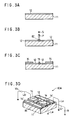
- Figure 3 shows more details of the process used to fabricate the MSM photo-receiving device 10A of Figure 2 according to the method of this invention.
- a full-surface conductive layer 12 of titanium is deposited on a GaAs semiconductor substrate 11.
- a STM probe P is positioned near a prescribed surface portion of the titanium layer 12, as shown in Figure 3 (B), and a potential of 5 V is applied between the probe P and the layer 12 under atmospheric conditions (that is, in an environment that includes moisture), setting up a tunneling current, while at the same time the probe is scanned in a direction S normal to the drawing sheet.
- the scanning speed is set to produce a titanium oxide line 15' having a width of 100 nm.
- mounting electrodes 14 of Ti/Au are formed at a desired portion on the electrodes 12 to facilitate a connection to an external circuit that may be required.
- ground electrodes 14' of Ti/Au are formed parallel to a stripe that includes electrodes 12 and optical guide 15. In this example, stripes are each 5 ⁇ m wide and are 5 ⁇ m apart. This enables a bias line Lb that applies a bias voltage Vb to be connected to one of the electrodes 12, and a signal line Lr to a resistance load R to be connected to the other electrode 12, and a ground line Le to be connected to each of the ground electrodes 14' forming a shield structure.
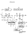
- the measurement system shown in Figure 4 was used to evaluate the thus-fabricated photo-receiving device 10A, using the electro-optical sampling method.
- This is a method in which polarization changes in a laser beam corresponding to changes in the electrical field of an electro-optical crystal disposed on the circuit to be measured are detected, producing an electrical signal that is measured at a time resolution in the femtosecond range.
- the light source was a colliding pulse mode-locked (CPM) dye laser 22, fed by an argon ion laser 21, with an output of around 10 mW, an output pulse width of 40 fs, and a wavelength of 620 nm.
- CCM colliding pulse mode-locked
- the titanium oxide optical guide 15 of the photo-receiving device 10A exhibited adequate transparency to this light of wavelength 620 nm, and satisfactory electrical insulation properties.
- the beam from the CPM dye laser 22 is split by a 9:1 beam splitter 23 into an exciting beam I P and a sampling beam Is, respectively.
- the exciting beam I P is passed through a variable delay apparatus 32 to adjust the difference with respect to the light path of the sampling beam Is, and is then directed into the optical guide 15 of the photo-receiving device 10A.
- the sampling beam Is is passed through a half-wave plate 24 and polarizer 25 to adjust the polarization direction, and then into an electro-optical (EO) probe 31.
- EO electro-optical
- the EO probe 31 is a LiTaO 3 plate 300 ⁇ m long, 250 ⁇ m wide and 50 ⁇ m thick, with an electro-optical coefficient of 35.8 pm/V, and has a multilayer, dielectric antireflection coating on the rear surface of the crystal in contact with the photo-receiving device.
- the crystal orientation of the EO probe 31 and the polarization direction of the sampling beam Is are set for optimum sensitivity with respect to an electrical field perpendicular to the stripe.
- the reflected sampling beam Is phase modulated by electrical field permeation into the EO probe 31 is subjected to phase compensation by a Babinet-Soleil compensator 26, deflected by a polarizing beam splitter 27 and intensity modulated by a pair of photoreceivers 28a and 28b.
- the outputs of the photoreceivers 28a and 28b are passed through a differential amplifier 29 to a lock-in amplifier 34 and thereby locked in to the same 1 MHz that is applied to the fabricated device by a signal generator 33.
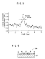
- Figure 5 displays a plot of the measurement results based on the output of the lock-in amplifier 34.
- the vertical axis is field strength and the horizontal axis is time.
- the device fabrication of this invention makes it possible to define the region for the optical window 13 and to form the protective insulation structure (optical guide) 15 for the optical window 13 in a single process.
- the optical window 13 enables the optical window 13 to be formed to a width as fine as around 100 nm, so it does not exceed the wavelength of the light to be detected, and the formation of a protective insulation structure 15 that exhibits high quality and high dielectric resistance.
- Applying the method to the fabrication of an MSM photo-receiving device results in a device that combines high speed with high sensitivity.
- the width W of the optical window 13 is no larger than the wavelength of the light to be detected, the light I P impinging on the light-absorbing substrate 11 appears as an evanescent photoelectric field, the photoelectric field strength is increased just in the vicinity of the surface of the substrate 11 and the incident light is absorbed in this substrate 11 surface vicinity.
- the photo-receiving device 10A is provided with the high quality protective insulation structure 15, with its high dielectric resistance, compared to a conventional device a higher voltage can be applied across the electrodes 12, and the electrical field strength is therefore higher at the surface than inside the substrate, excited carriers (electrons and holes) generated by the incident light I P in the vicinity of the surface of the substrate 11, close to the electrodes 12, are drawn at high speed to the respective electrode (the relatively positive electrode in the case of electrons, and relatively negative electrode in the case of holes). In other words, photoelectric conversion (photodetection) can be effected at a higher speed.
- the high speed at which the carriers are drawn away as a result of the high voltage applied means that less recombination takes place, which helps to increase the sensitivity and output power of the device.
- This invention provides a device that is faster and more sensitive than a conventional device. This is because even if, in the device of this invention, the width W of the gap between the electrodes 12 is increased to more than the 300 nm of a conventional device, while observing the provision that the width W does not exceed the wavelength of the light to be detected, the lower risk of a dielectric breakdown occurring means that a higher voltage can be applied across the electrodes 12. Doing this would ease the fabrication process burden.
- An example is the above-described processing method in which a scanning probe apparatus is applied to the formation of the protective insulation structure 15; for example, forming an oxide line of a desired width by oscillating the probe P to each side of the scan line, as described above.
- a different existing fine pattern process technology such as electron beam lithography or selective epitaxis.
- the protective insulation structure/optical guide 15 does not have to be an insulator. It is only required that it be located between the electrodes 12 and exhibit higher resistance than that of the substrate 11, and as such may be formed of a semiconductor based on an insulation material. If GaAs is used for the substrate 11, for light-permeability (minimal photo-absorption) the structure 15 could be formed of AlAs, GaP or other such semiconductor having a larger band-gap than that of the GaAs. However, when such a semiconductor is used to form the optical guide 15, to ensure complete insulation a small gap should be left between the guide 15 and at least one of the electrodes 12 and this gap filled with an insulation material. This corresponds to an embodiment in which the optical guide 15 is constituted of materials having different properties.
- Figure 6 shows an embodiment of a photo-receiving device 10B in which the optical window is provided with two or more discernible optical guides 15 (only two are shown in the drawing), and a nontransparent interstitial portion or means 12' is provided between adjacent guides 15.
- the detection sensitivity can be increased by the number of optical guides 15 having a width not exceeding the wavelength of the light to be detected.
- the interstitial means 12' may be conductive or insulative, but preferably are conductive, since that enables them to be formed of the same material as the film used to form the electrodes 12 at each side. Any desired fine pattern process technology may be used to form the optical guides 15.
- a scanning probe based process is highly rational, as it enables the process used to form the guides 15 to be utilized to also form the electrodes 12 and interstitial means 12', all at the same time.
- the optical guides 15 may be formed of a mixed multiplicity of materials having different properties, such as insulators and semiconductors, as long as this does not depart from the defined scope of the invention.
- the optical guides 15 may include a structure that enables the optical properties of the guides to be varied. Such a facility is included in the device 10C shown in Figure 7.
- part of the optical guide 15 formed in the optical window has a multilayer structure comprising, from the side in contact with the substrate 11, an n-type (or p-type) semiconductor layer 37, a GaAs/AlGaAs or InAs/InGaAs superlattice layer 39, and a p-type (or n-type) semiconductor layer 38.
- a nontransparent protective insulation structure 15" formed of a single insulation or semiconductor material.
- a contact electrode 36 of a metal or semiconductor substance is provided that extends down through the structure 15" to form an electrical contact with the semiconductor layer 38.
- the semiconductor layer 37 is also provided with a control electrode.
- one of the electrodes 12 (the one on the left of the drawing) also functions as this contact electrode.
- an electrical field can be applied to the superlattice layer 39 by applying an external voltage between one of the electrodes 12 and the control electrode 36.
- the quantum containment Stark effect corresponding to the strength of the electrical field changes the absorption coefficient and refractive index with respect to wavelengths in the vicinity of the ends of the bands, making it possible to control the absorption peak of the excitons, the appearance of which is a characteristic feature of quantum structures.
- the spectrum of the incident light I P can therefore be established from changes in the absorption coefficient for each wavelength, which can be used to improve the functional quality and range of a photo-receiving device.
- a Fabry-Perot resonator structure can be incorporated in the optical guide 15 to provide a photo-receiving device with wavelength selectivity, as the resonance wavelength can then be controlled by using the application of an outside voltage to electrodes 12 and 36 to control the refractive index.
- Such an arrangement could be envisaged, with reference to Figure 7, by viewing the superlattice layer 39 as the requisite internal waveguide of the resonator and the upper and lower layers 37 and 38 as being both reflectors and refractivity control electrodes.
- such an embodiment also includes other structures for controlling optical properties.
- an insulation layer 40 is disposed between the electrode 12 on the right and the optical guide 15 that includes the superlattice layer 39, to prevent the semiconductor layer 37 from causing an electrical short between the electrodes 12.
- a gap may be used for this instead of the insulation layer 40, providing the layer 40 is not complex, since it can be formed at the same time as the insulation structure 15".
Abstract
Description
- The present invention relates to an improved photo-receiving device for converting light signals to electrical signals, as required in such fields as communications and information processing, and to an improved method of fabricating a photo-device, which also means a light emitting device for converting electrical signals to light signals.
- The term photoelectric conversion as used herein refers to the function of converting a light signal to an electrical signal in a photo-receiving device, and also to the function of converting an electrical signal to a light signal in a light emitting device. Figure 8 illustrates the structure of a conventional photo-
receiving device 50 as described in the IEEE Journal of Quantum Electronics (Vol. 28, pp. 2358-2368, 1992) for converting light signals to electrical signals at a relatively high speed. As shown, the photo-receiving device 50 comprises asubstrate 11 that constitutes the photoelectric conversion portion (which can also be referred to as a light-absorbing portion, as this is a photo-receiving device), and a pair ofopposed electrode portions 51, each in the form of a thin film of metal, formed on the surface of thesubstrate 11. The exposed surface of thesubstrate 11 between theelectrodes 51 forms anoptical window 13 for the entry of the light IP to be detected. - When light IP impinges on the
optical window 13 while an appropriate voltage is being applied to the pair ofelectrodes 51, excited carriers (electrons and holes) are generated in thesubstrate 11. Holes, shown in the drawing as blank circles, are drawn to theelectrode 51 with the relatively negative (-) potential, and electrons, shown as solid circles, are drawn to theelectrode 51 with the relatively positive (+) potential, setting up a flow of a photoelectric current (photo detection current) which takes place via theelectrodes 51, whereby the incidence of the light IP is detected. - With this type of conventional photo-
receiving device 50 of Figure 8, which is generally referred to as a MSM (metal/semiconductor/metal) device, the smaller the width W of theoptical window 13, that is, the smaller the distance between theelectrodes 51, the faster the operating speed of the device is, and raising the applied voltage increases device speed and sensitivity. Also, making the width W of theoptical window 13 no larger than the wavelength of the light IP to be detected imparts an evanescent field to the light IP impinging on the light-absorbingsubstrate 11 and causes the incident light IP to be absorbed in the vicinity of the surface of thesubstrate 11. At the same time, as the field strength set up by theelectrodes 51 is higher at the surface of thesubstrate 11 than in the interior, the excited carriers generated in the vicinity of the surface of thesubstrate 11 are drawn rapidly to theelectrodes 51, enabling higher speed operation to be achieved and the affect of carrier recombination to be reduced. - In the case of the photo-receiving
device 50 of Figure 8, reducing the width W between theelectrodes 51 to around 300 nm by means of electron beam lithography, an existing fine pattern process technology, resulted in a pulse-response full width at half maximum output of 870 fs, which is quite a high speed compared to other photo-receiving devices. However, it is difficult to achieve higher speeds, for the following reasons. - A first problem is that, since the
optical window 13 on the surface of thesubstrate 11 between theelectrodes 51 is exposed, applying a higher voltage across theelectrodes 51 giving rise to creeping discharge along the exposed surface of theoptical window 13 and air-gap discharge, rendering the device unusable. That is, if the width W between theelectrodes 51 is reduced beyond a certain limit, even a low voltage causes a dielectric breakdown. On the other hand, even in cases where the width W of theincident light window 13 can be increased, within the limitation that it does not exceed the wavelength of the incident light IP, there are major constraints on the voltage that can be applied. A second problem is that of the limits of the process technology. Even with existing electron beam lithography, a relatively high precision fine pattern process technology, an electrode gap cannot really be precision-fabricated to a width W of 100 nm or less, and even 300 nm or less is quite difficult. - A conventional method of resolving the first problem is to cover, or bury, the exposed surface portion constituting the
optical window 13 between theelectrodes 51. This will now be described, with reference to Figure 9. The following description is not limited to photo-receiving devices, being also applicable to devices, such as light emitting devices, having a light emitting area defined in the form of an optical window. Thus,reference numeral 52 is used to denote the photo-device shown in Figure 9, the light-absorbingportion 11 of Figure 8 is the photoelectric conversion portion in the general meaning of the term, and the termmetallic film electrodes 51 is encompassed by the term optically nontransparent conductive film (electrodes) 12. To fabricate the photo-device 52, existing lithographic technology is used to remove a prescribed region of an optically nontransparentconductive film 12 formed onphotoelectric conversion portion 11, thereby exposing a defined portion that forms anoptical window 13. - Sputtering or another such vapor deposition technique is then used to form an optically transparent
protective insulation layer 53 over theoptical window 13. However, sputtering and other such vacuum vapor deposition apparatuses are costly, so there is no objection to achieving the required result by other means. Also, while the optically nontransparentconductive film 12 in which theoptical window 13 region is formed (defined) and theinsulation layer 53 to protect theoptical window 13 are formed using separate processes, device fabrication can be simplified by effecting both processes in one step. As described, even with the relatively high patterning precision provided by a technology such as electron beam lithography, the minimum width W of theoptical window 13 that can be formed in the optically nontransparentconductive film 12 is in the order of 300 nm. - Non-uniformities in the thickness of the surface deposition film gives rise to variation in device characteristics, and high frequency characteristics can be degraded by dielectric deposits. When a very fine optical window is used, forming a high-quality insulative film over the window that has high dielectric resistance is difficult.
- An object of the present invention is to provide a high speed photo-receiving device in which constraints relating to the width W of the optical window between electrodes, and to the applied voltage, are reduced.
- Another object of the present invention is to provide a photo-receiving device that is more highly functional and multifunctional than conventional photo-receiving devices.
- Yet another object of the present invention is to provide a method of fabricating a photo-device wherein an optical window region and a protective layer over the optical window surface can be formed in one step.
- A further object of the present invention is to provide a method of fabricating a photo-device that enables the above-described drawbacks to be resolved or alleviated and an optical window to be formed to have a smaller width than that of conventional photo-devices.
- According to one aspect of the present invention, there is provided a photo-receiving device, comprising a light-absorbing substrate, a pair of electrodes disposed on a surface of the light-absorbing substrate, an optical window through which light to be detected enters, said optical window being an exposed surface portion of the substrate between the electrodes, and an optical guide structure provided on the exposed surface portion of the substrate between the electrodes, said optical guide being permeable to the light to be detected, having a width that does not exceed a wavelength of the light to be detected, and exhibiting a higher resistance than that of the substrate.
- With this configuration, the electrodes can be brought closer together than in a conventional configuration without risk of dielectric breakdown between the electrodes. This means a stronger electrical field can be applied, which increases the speed of the photocarriers and reduces the effect of carrier recombination, resulting in a photo-receiving device that exhibits high speed as well as high sensitivity. Moreover, the optical guide also serves as a protective layer over the exposed surface portion of the substrate that constitutes the optical window. This eliminates the need to separately form a protective layer, thereby simplifying the fabrication process and reducing fabrication cost.
- In the photo-receiving device, the optical guide is formed of an insulating material. The insulator may be an oxide of the thin film material used to constitute the electrodes. The optical guide may be formed of a semiconductor material, provided the semiconductor material exhibits higher resistance than the light-absorbing substrate. The optical guide may be formed of materials having different properties.
- According to another aspect of the invention, there is provided a photo-receiving device in which optical guide properties such as refractive index, absorption coefficient, polarization direction and the like can be varied. In such an arrangement, control electrodes can be included to apply voltage for effecting the adjustment of the optical properties of the optical guide. At least one of the control electrodes may be constituted by one of the above-described pair of electrodes. A semiconductor superlattice structure or Fabry-Perot resonator are representative examples of the type of arrangement that may be used to vary the optical properties of the optical guide.
- In the photo-receiving device, the insulation creepage distance between the electrodes is increased by making the thickness of the optical guide greater than the thickness of the electrodes. The photo-receiving device has a plurality of optical guides arranged in parallel between the pair of electrodes, and means each provided between adjacent optical guides so as not to transmit the light to be detected.
- According to another aspect of the present invention, there is provided a method of fabricating a photo-device comprising a step of forming an optically nontransparent, electrically conductive layer on a surface of a photoelectric conversion substrate, and a step whereby a portion of the optically nontransparent, electrically conductive layer is transformed to form over the optical window a light-permeable protective insulation structure of a prescribed width and length, and at the same time define an optical window region on the substrate surface beneath the protective insulation structure.
- The optically nontransparent, electrically conductive layer may be of a metal or an alloy, or a semiconductor (including semi-insulators), or may include a semiconductor superlattice structure.
- In this way, a photo-device is fabricated to have a prescribed area on a surface of the photo-receiving or photoemitting photoelectric conversion substrate forming an optical window of a prescribed width via which light is received or emitted. When it is a photo-device that requires that an optically nontransparent, electrically conductive layer be formed at each side of the optical window, the defined optical window region and an insulation structure for protecting the optical window can be formed in a single step. This is highly efficient and eliminates the need to use a costly vacuum vapor deposition apparatus to form the protective layer over the entire surface.
- In this method, the optically nontransparent, electrically conductive layer is transformed by oxidation. This oxidation can be effected using a scanning probe apparatus.
- With this method, a fine optical window having a width that does not exceed the wavelength of the light to be detected, and a high-quality, highly dielectrically-resistant protective insulative structure for the optical window can both be formed by the same step. The result is that carrier speed is increased by applying a high field strength while the effect of carrier recombination is decreased, thus providing a photo-device that is faster and more sensitive.
- There is a case where multiple mutually separated portions of the optically nontransparent, electrically conductive layer are transformed.
- The photoelectric conversion substrate is of a light-absorbing material having a light receiving function, a non-transformed portion of the optically nontransparent, electrically conductive layer functions as an electrode to apply a voltage to the light-absorbing substrate, and the protective insulation structure functions as an optical guide that directs light to the substrate.
- According to another aspect of the present invention, there is provided a method of fabricating a photo-device whereby the thickness of the protective insulation structure preferably is thicker than the thickness of the non-transformed portions of the optically nontransparent, electrically conductive layer at each side, and when said portions of the layer remaining at each side are utilized as a pair of electrodes, the insulation creepage distance between the electrodes is increased, thereby increasing the resistance to dielectric breakdown.
- Further features of the invention, its nature and various advantages will be more apparent from the accompanying drawings, in which:
- Figure 1 illustrates a method of fabricating the photo-device according to an embodiment of the invention;
- Figure 2 shows the general configuration of an embodiment of the photo-receiving device of the invention;
- Figure 3 illustrates steps used in the fabrication of an MSM photo-receiving device in accordance with the method of fabricating a photo-device of the invention;
- Figure 4 is a diagram of a system used to measure a photo-receiving device fabricated by the steps of Figure 3;
- Figure 5 shows the measurement results obtained with the fabricated photo-receiving device;
- Figure 6 shows the configuration of another photo-receiving device fabricated according to the method of the invention;
- Figure 7 shows the configuration of another photo-receiving device fabricated according to the method of the invention;
- Figure 8 shows the arrangement of a conventional MSM photo-receiving device; and
- Figure 9 illustrates a conventional protective structure for an optical window.
- Figure 1 shows an example of basic steps or processes used to fabricate a photo-device according to the method of the invention. In this and other embodiments, parts corresponding to parts in the
conventional devices - Figure 1 (A) shows a conductive, optically
nontransparent film layer 12 formed on a surface of a light receiving or light emittingphotoelectric conversion substrate 11. The internal constitution of thesubstrate 11 is not specifically defined by the invention, and may be comprised in accordance with existing device structural principles. If the device is formed as a conventional MSM photo-receiving device, as described in the foregoing, thesubstrate 11 will function as a light-absorber, and in terms of material, will be formed of a bulk semiconductor such as GaAs. Thefilm 12 may be formed of a suitable metal (including alloys) or semiconductor, including a semiconductor having a superlattice structure. In broad terms, a material that is at least non-permeable, or has very low permeability, to the light to be detected, in the case of a photo-receiving device, and to the emitted light, in the case of a light-emitting device, and has significant electrical conductivity, can be regarded as being applicable for the purpose of the invention. - Starting from the structure shown in Figure 1 (A), the properties of a region of the optically
nontransparent layer 12 corresponding to a region 13' in which anoptical window 13 will ultimately be formed are transformed to form an insulation structure that is light-permeable (that is, transparent or semitransparent to light that is to be detected or transmitted, as the case may be). Preferably this is done by using a scanning probe apparatus to oxidize the region concerned. A scanning tunneling microscope (STM) and an atomic force microscope (AFM) are examples of apparatuses that can be used for this. In the case of an STM, for example, the tip of the probe P is brought close to thefilm 12 and a power source V is used to apply a high-voltage electrical field across the space between the probe tip and thefilm 12 while at the same time the probe P is scanned in a direction S. This oxidizes thefilm 12 along the line of the scan, forming an insulation line 15' that is light-permeable. Using this method, the present inventors were able to form a titanium oxide line with a minimum width of 18 nm by oxidizing a titanium layer deposited on a GaAs substrate. The same result was also obtained with an AFM. While not directly related to this invention, with an AFM the target film does not have to be electrically conductive. - When the line 15' has been formed to the prescribed length, a light-permeable
protective insulation structure 15 having a prescribed width and length is formed to protect the optical window, and the same formation process is used to define a region for theoptical window 13 on the substrate surface beneath thestructure 15, as shown in Figure 1 (C). This simplifies the fabrication process by eliminating the need for separately forming a film over the entire surface for an optical window protective layer after first forming the optical window, such as is required in the case of the conventional device shown in Figure 9. - With a photo-
device 10 fabricated according to this invention, moreover, the remaining nontransformed portions of the optically nontransparentconductive film 12 at each side of theprotective insulation structure 15 can be used as electrodes. Since in such a case theinsulation structure 15 is disposed between theelectrodes 12, the insulation creepage distance is increased, enhancing the resistance to dielectric breakdown. Increasing the thickness of thestructure 15 to above a certain level also enhances insulation capabilities. - Thus, it is possible to apply a higher voltage across the
electrodes 12 while using around the same separation width W as a conventional device. Conversely, this means that for the same applied voltage, a higher field strength can be obtained in the vicinity of thesubstrate 11 by reducing the distance between theelectrodes 12. This is highly advantageous when the method of this invention is applied to the fabrication of an MSM photo-receiving device. With the use of a scanning probe apparatus to process the optically nontransparentconductive film 12, the width W of the optical window 13 (that is, the distance between the electrodes 12) can be reduced down to little more than ten nanometers, while at the same time ensuring the high insulation quality of theprotective structure 15. - Figure 2 is a cross-sectional view of a photo-receiving
device 10A according to the present invention. The photo-receivingdevice 10A comprises a light-absorbingsubstrate 11 of GaAs or other such suitable semiconductor on which a pair ofelectrodes 12 is formed, with the space between theelectrodes 12 forming anoptical window 13 for light entry. Theelectrodes 12 are usually of titanium or other such metal, but can also be formed of silicon or another such semiconductor which has been made conductive by the introduction of an appropriate impurity. The light-absorbingsubstrate 11 can be used as the structural substrate of the photo-receivingdevice 10A, this is not limitative, as the illustrated structure can be formed using a physical support substrate other than the one shown. - In the case of the conventional photo-receiving
device 50 shown in Figure 8, theoptical window 13 is in the form of a portion of the surface exposed to the air. In contrast, the optical window portion of the photo-receivingdevice 10A is provided with a protective insulation structure formed of a suitable insulation material such as titanium oxide, silicon oxide or silicon nitride. As well as protecting the optical window by covering the exposed portion of thesubstrate 11, thisstructure 15 also serves as an optical guide. Thisoptical guide 15 needs to at least be light-permeable, that is, transparent or semitransparent with respect to the light IP to be detected. The above are examples of materials that can be treated as transparent to light of most wavelengths. - Since in this arrangement the portion of the
substrate 11 between the electrodes is not exposed, it eliminates or alleviates the surface discharge on the exposed surface of thesubstrate window 13 that is a problem with the conventional arrangement, and, using the same width W betweenelectrodes 12 as a conventional configuration, enables a higher voltage to be applied. It is desirable to make the thickness t of theoptical guide 15 greater than the thickness of theelectrodes 12. Doing this increases the creeping distance between theelectrodes 12 by an amount corresponding to the increase in thickness, thus providing adequate resistance to the type of air gap discharge across theelectrodes 12 to which the conventional device arrangement is prone. Therefore, while in the case of a conventional device configuration the risk of dielectric breakdown imposes constraints on how close theelectrodes 12 can be brought together, thereby placing an upper limit on the voltage that can be applied, in the photo-receivingdevice 10A of this invention such constraints are considerably reduced. - As has been described in the foregoing, when the width W of the
optical window 13 is made to not exceed the wavelength of the light IP to be detected, the light IP impinging on the light-absorbingsubstrate 11 appears as an evanescent photoelectric field, the photoelectric field strength is increased just in the vicinity of the surface of thesubstrate 11 and the incident light IP is absorbed in said vicinity of thesubstrate 11 surface. Since in the inventive photo-receivingdevice 10A a higher voltage can be applied across theelectrodes 12 than in a conventional device, and the electrical field strength is therefore higher at the surface than inside the substrate, excited carriers (electrons and holes) generated by the incident light IP in the vicinity of the surface of thesubstrate 11, close to theelectrodes 12, are drawn at high speed to the respective electrode (the relatively positive electrode in the case of electrons, and relatively negative electrode in the case of holes). In other words, photoelectric conversion (photodetection) can be effected at a higher speed. Moreover, the high speed at which the carriers are drawn away as a result of the high voltage applied means that less recombination takes place, which helps to increase the sensitivity and output of the device. - Figure 3 shows more details of the process used to fabricate the MSM photo-receiving
device 10A of Figure 2 according to the method of this invention. With reference first to Figure 3 (A), a full-surface conductive layer 12 of titanium is deposited on aGaAs semiconductor substrate 11. A STM probe P is positioned near a prescribed surface portion of thetitanium layer 12, as shown in Figure 3 (B), and a potential of 5 V is applied between the probe P and thelayer 12 under atmospheric conditions (that is, in an environment that includes moisture), setting up a tunneling current, while at the same time the probe is scanned in a direction S normal to the drawing sheet. The scanning speed is set to produce a titanium oxide line 15' having a width of 100 nm. Considerable control over the width and thickness of the line 15' can be exercised by adjusting the voltage and scanning speed. The width of the line 15' can be increased by also oscillating the probe P to each side of the scan line. The titanium line 15' thus formed to a prescribed length constitutes theoptical guide 15, and the non-oxidized portions of the titanium layer at eachside form electrodes 12. Thus, the fabrication of theelectrodes 12 and theoptical guide 15 between theelectrodes 12 is rationalized into a single procedure. - With reference to Figure 3 (C), mounting
electrodes 14 of Ti/Au, for example, are formed at a desired portion on theelectrodes 12 to facilitate a connection to an external circuit that may be required. With reference to Figure 3 (D), ground electrodes 14' of Ti/Au, for example, are formed parallel to a stripe that includeselectrodes 12 andoptical guide 15. In this example, stripes are each 5 µm wide and are 5 µm apart. This enables a bias line Lb that applies a bias voltage Vb to be connected to one of theelectrodes 12, and a signal line Lr to a resistance load R to be connected to theother electrode 12, and a ground line Le to be connected to each of the ground electrodes 14' forming a shield structure. - The measurement system shown in Figure 4 was used to evaluate the thus-fabricated photo-receiving
device 10A, using the electro-optical sampling method. This is a method in which polarization changes in a laser beam corresponding to changes in the electrical field of an electro-optical crystal disposed on the circuit to be measured are detected, producing an electrical signal that is measured at a time resolution in the femtosecond range. The light source was a colliding pulse mode-locked (CPM)dye laser 22, fed by anargon ion laser 21, with an output of around 10 mW, an output pulse width of 40 fs, and a wavelength of 620 nm. The titanium oxideoptical guide 15 of the photo-receivingdevice 10A exhibited adequate transparency to this light of wavelength 620 nm, and satisfactory electrical insulation properties. The beam from theCPM dye laser 22 is split by a 9:1beam splitter 23 into an exciting beam IP and a sampling beam Is, respectively. The exciting beam IP is passed through avariable delay apparatus 32 to adjust the difference with respect to the light path of the sampling beam Is, and is then directed into theoptical guide 15 of the photo-receivingdevice 10A. The sampling beam Is is passed through a half-wave plate 24 andpolarizer 25 to adjust the polarization direction, and then into an electro-optical (EO)probe 31. TheEO probe 31 is a LiTaO3 plate 300 µm long, 250 µm wide and 50 µm thick, with an electro-optical coefficient of 35.8 pm/V, and has a multilayer, dielectric antireflection coating on the rear surface of the crystal in contact with the photo-receiving device. The crystal orientation of theEO probe 31 and the polarization direction of the sampling beam Is are set for optimum sensitivity with respect to an electrical field perpendicular to the stripe. - The reflected sampling beam Is phase modulated by electrical field permeation into the
EO probe 31 is subjected to phase compensation by a Babinet-Soleil compensator 26, deflected by apolarizing beam splitter 27 and intensity modulated by a pair ofphotoreceivers photoreceivers differential amplifier 29 to a lock-inamplifier 34 and thereby locked in to the same 1 MHz that is applied to the fabricated device by asignal generator 33. Figure 5 displays a plot of the measurement results based on the output of the lock-inamplifier 34. The vertical axis is field strength and the horizontal axis is time. With measurements taken at a point 70 µm from the photo-receivingdevice 10A, a full width at half maximum (FWHM) electrical-pulse value of 570 fs was obtained. At a 3dB region this is equivalent to 790 GHz, which, without dispute, is at this point world record speed for this type of photoconductive photo-receiving device. - Thus, the device fabrication of this invention makes it possible to define the region for the
optical window 13 and to form the protective insulation structure (optical guide) 15 for theoptical window 13 in a single process. In addition to this basic effect, it enables theoptical window 13 to be formed to a width as fine as around 100 nm, so it does not exceed the wavelength of the light to be detected, and the formation of aprotective insulation structure 15 that exhibits high quality and high dielectric resistance. Applying the method to the fabrication of an MSM photo-receiving device results in a device that combines high speed with high sensitivity. - Specifically, when the width W of the
optical window 13 is no larger than the wavelength of the light to be detected, the light IP impinging on the light-absorbingsubstrate 11 appears as an evanescent photoelectric field, the photoelectric field strength is increased just in the vicinity of the surface of thesubstrate 11 and the incident light is absorbed in thissubstrate 11 surface vicinity. Because the photo-receivingdevice 10A is provided with the high qualityprotective insulation structure 15, with its high dielectric resistance, compared to a conventional device a higher voltage can be applied across theelectrodes 12, and the electrical field strength is therefore higher at the surface than inside the substrate, excited carriers (electrons and holes) generated by the incident light IP in the vicinity of the surface of thesubstrate 11, close to theelectrodes 12, are drawn at high speed to the respective electrode (the relatively positive electrode in the case of electrons, and relatively negative electrode in the case of holes). In other words, photoelectric conversion (photodetection) can be effected at a higher speed. Moreover, the high speed at which the carriers are drawn away as a result of the high voltage applied means that less recombination takes place, which helps to increase the sensitivity and output power of the device. This invention provides a device that is faster and more sensitive than a conventional device. This is because even if, in the device of this invention, the width W of the gap between theelectrodes 12 is increased to more than the 300 nm of a conventional device, while observing the provision that the width W does not exceed the wavelength of the light to be detected, the lower risk of a dielectric breakdown occurring means that a higher voltage can be applied across theelectrodes 12. Doing this would ease the fabrication process burden. An example is the above-described processing method in which a scanning probe apparatus is applied to the formation of theprotective insulation structure 15; for example, forming an oxide line of a desired width by oscillating the probe P to each side of the scan line, as described above. Instead, it would be possible to use a different existing fine pattern process technology, such as electron beam lithography or selective epitaxis. - Modifications of the invention will now be described. First, the protective insulation structure/
optical guide 15 does not have to be an insulator. It is only required that it be located between theelectrodes 12 and exhibit higher resistance than that of thesubstrate 11, and as such may be formed of a semiconductor based on an insulation material. If GaAs is used for thesubstrate 11, for light-permeability (minimal photo-absorption) thestructure 15 could be formed of AlAs, GaP or other such semiconductor having a larger band-gap than that of the GaAs. However, when such a semiconductor is used to form theoptical guide 15, to ensure complete insulation a small gap should be left between theguide 15 and at least one of theelectrodes 12 and this gap filled with an insulation material. This corresponds to an embodiment in which theoptical guide 15 is constituted of materials having different properties. - Figure 6 shows an embodiment of a photo-receiving
device 10B in which the optical window is provided with two or more discernible optical guides 15 (only two are shown in the drawing), and a nontransparent interstitial portion or means 12' is provided between adjacent guides 15. The detection sensitivity can be increased by the number ofoptical guides 15 having a width not exceeding the wavelength of the light to be detected. In principle the interstitial means 12' may be conductive or insulative, but preferably are conductive, since that enables them to be formed of the same material as the film used to form theelectrodes 12 at each side. Any desired fine pattern process technology may be used to form the optical guides 15. A scanning probe based process is highly rational, as it enables the process used to form theguides 15 to be utilized to also form theelectrodes 12 and interstitial means 12', all at the same time. - As has already been mentioned, it is possible for the
optical guides 15 to be formed of a mixed multiplicity of materials having different properties, such as insulators and semiconductors, as long as this does not depart from the defined scope of the invention. Moreover, the optical guides 15 may include a structure that enables the optical properties of the guides to be varied. Such a facility is included in thedevice 10C shown in Figure 7. In this arrangement, part of theoptical guide 15 formed in the optical window has a multilayer structure comprising, from the side in contact with thesubstrate 11, an n-type (or p-type)semiconductor layer 37, a GaAs/AlGaAs or InAs/InGaAs superlattice layer 39, and a p-type (or n-type)semiconductor layer 38. On top of this is a nontransparentprotective insulation structure 15" formed of a single insulation or semiconductor material. For external control of optical properties, acontact electrode 36 of a metal or semiconductor substance is provided that extends down through thestructure 15" to form an electrical contact with thesemiconductor layer 38. Thesemiconductor layer 37 is also provided with a control electrode. In this example, one of the electrodes 12 (the one on the left of the drawing) also functions as this contact electrode. - With this arrangement, an electrical field can be applied to the
superlattice layer 39 by applying an external voltage between one of theelectrodes 12 and thecontrol electrode 36. The quantum containment Stark effect corresponding to the strength of the electrical field changes the absorption coefficient and refractive index with respect to wavelengths in the vicinity of the ends of the bands, making it possible to control the absorption peak of the excitons, the appearance of which is a characteristic feature of quantum structures. The spectrum of the incident light IP can therefore be established from changes in the absorption coefficient for each wavelength, which can be used to improve the functional quality and range of a photo-receiving device. A Fabry-Perot resonator structure can be incorporated in theoptical guide 15 to provide a photo-receiving device with wavelength selectivity, as the resonance wavelength can then be controlled by using the application of an outside voltage toelectrodes superlattice layer 39 as the requisite internal waveguide of the resonator and the upper andlower layers - In the configuration shown in Figure 7, an
insulation layer 40 is disposed between theelectrode 12 on the right and theoptical guide 15 that includes thesuperlattice layer 39, to prevent thesemiconductor layer 37 from causing an electrical short between theelectrodes 12. Although a gap may be used for this instead of theinsulation layer 40, providing thelayer 40 is not complex, since it can be formed at the same time as theinsulation structure 15". - Other modifications and variations of the present invention clearly are also possible in light of the above teachings. It is therefore to be understood that within the scope of the appended claims, the invention may be practiced otherwise than as specifically described herein.
Claims (21)
- A photo-receiving device, comprising a light-absorbing substrate 11, a pair of electrodes 12 disposed on a surface of the light-absorbing substrate, an optical window 13 through which light to be detected enters, said optical window being an exposed surface portion of the substrate between the electrodes, and an optical guide 15 provided on the exposed surface portion of the substrate between the electrodes, said optical guide being permeable to the light to be detected, having a width W that does not exceed a wavelength of the light to be detected, and exhibiting a higher resistance than that of the substrate.
- A photo-receiving device according to claim 1, wherein the optical guide 15 is formed of an insulator.
- A photo-receiving device according to claim 2, wherein the insulator is formed by oxidation of a material used to form the electrodes 12.
- A photo-receiving device according to claim 1, wherein the optical guide 15 is formed of a semiconductor.
- A photo-receiving device according to claim 1, wherein the optical guide 15 includes materials having different properties.
- A photo-receiving device according to claim 1, wherein the optical guide 15 includes a variable structure for varying optical properties of the optical guide.
- A photo-receiving device according to claim 6, wherein the variable structure has control electrodes for receiving a voltage applied for varying optical properties of the optical guide.
- A photo-receiving device according to claim 7, wherein one of the pair of electrodes 12 forms at least one of the control electrodes.
- A photo-receiving device according to claim 6, wherein the variable structure includes a semiconductor superlattice structure.
- A photo-receiving device according to claim 6, wherein the variable structure includes a Fabry-Perot resonator structure.
- A photo-receiving device according to claim 1, wherein the optical guide 15 is thicker than the pair of electrodes 12.
- A photo-receiving device according to claim 1, wherein the optical guide comprises a pair of optical guide means 15 arranged in parallel between the pair of electrodes 12, and a space between said pair of optical guide means is provided with an interstitial means 12' that is nontransparent with respect to the light to be detected.
- A photo-receiving device according to claim 1, wherein the optical guide comprises multiple optical guide means 15 arranged in parallel between the pair of electrodes 12, and spaces between adjacent optical guides are provided with interstitial means 12' that are nontransparent with respect to the light to be detected.
- A method of fabricating a photo-device, comprising a step of forming an optically nontransparent, electrically conductive layer 12 on a surface of a photoelectric conversion substrate 11, and a step whereby a portion of the optically nontransparent, electrically conductive layer is transformed to form over an optical window 13 a light-permeable protective insulation structure 15 of a prescribed width and length, and at the same time define a region of the optical window on the substrate surface beneath the light-permeable protective insulation structure.
- A fabrication method according to claim 14, wherein the optically nontransparent, electrically conductive layer 12 is of a metal or an alloy.
- A fabrication method according to claim 14, wherein the optically nontransparent, electrically conductive layer 12 is a semiconductor.
- A fabrication method according to claim 14, wherein the optically nontransparent, electrically conductive layer 12 includes a semiconductor superlattice structure.
- A fabrication method according to claim 14, wherein the transformation is oxidation.
- A fabrication method according to claim 18, wherein the oxidation is effected with a scanning probe process apparatus.
- A fabrication method according to claim 19, wherein the portion of the optically nontransparent, electrically conductive layer 12 that is transformed is transformed in multiple mutually separated locations on said layer.
- A fabrication method according to claim 14, wherein the photoelectric conversion substrate 11 is a light-absorbing substrate with a photo-receiving function,non-transformed portions of the nontransparent, electrically conductive layer 12 function as electrodes for applying a voltage to the photoelectric conversion substrate, andthe light-permeable protective insulation structure 15 functions as an optical guide for directing light into the light-absorbing substrate.
Priority Applications (1)
| Application Number | Priority Date | Filing Date | Title |
|---|---|---|---|
| EP99200499A EP0926742B1 (en) | 1995-01-23 | 1996-01-22 | Method of fabricating a photo-receiving device |
Applications Claiming Priority (6)
| Application Number | Priority Date | Filing Date | Title |
|---|---|---|---|
| JP8082/95 | 1995-01-23 | ||
| JP8083/95 | 1995-01-23 | ||
| JP7008083A JP2705757B2 (en) | 1995-01-23 | 1995-01-23 | Light receiving element |
| JP808295A JP2666888B2 (en) | 1995-01-23 | 1995-01-23 | Optical device manufacturing method |
| JP808395 | 1995-01-23 | ||
| JP808295 | 1995-01-23 |
Related Child Applications (1)
| Application Number | Title | Priority Date | Filing Date |
|---|---|---|---|
| EP99200499A Division EP0926742B1 (en) | 1995-01-23 | 1996-01-22 | Method of fabricating a photo-receiving device |
Publications (3)
| Publication Number | Publication Date |
|---|---|
| EP0723302A2 true EP0723302A2 (en) | 1996-07-24 |
| EP0723302A3 EP0723302A3 (en) | 1997-04-09 |
| EP0723302B1 EP0723302B1 (en) | 2001-08-22 |
Family
ID=26342522
Family Applications (2)
| Application Number | Title | Priority Date | Filing Date |
|---|---|---|---|
| EP96300405A Expired - Lifetime EP0723302B1 (en) | 1995-01-23 | 1996-01-22 | Photo-receiving device |
| EP99200499A Expired - Lifetime EP0926742B1 (en) | 1995-01-23 | 1996-01-22 | Method of fabricating a photo-receiving device |
Family Applications After (1)
| Application Number | Title | Priority Date | Filing Date |
|---|---|---|---|
| EP99200499A Expired - Lifetime EP0926742B1 (en) | 1995-01-23 | 1996-01-22 | Method of fabricating a photo-receiving device |
Country Status (3)
| Country | Link |
|---|---|
| US (3) | US5661328A (en) |
| EP (2) | EP0723302B1 (en) |
| DE (2) | DE69636016T2 (en) |
Cited By (2)
| Publication number | Priority date | Publication date | Assignee | Title |
|---|---|---|---|---|
| WO2013172815A1 (en) * | 2012-05-14 | 2013-11-21 | The Johns Hopkins University | Simplified devices utilizing novel pn-semiconductor structures |
| US8860078B2 (en) | 2012-05-14 | 2014-10-14 | The Johns Hopkins University | Simplified devices utilizing novel pn-semiconductor structures |
Families Citing this family (22)
| Publication number | Priority date | Publication date | Assignee | Title |
|---|---|---|---|---|
| DE19737498C2 (en) * | 1997-08-28 | 2002-09-12 | Deutsche Telekom Ag | Optical connection |
| FR2803950B1 (en) | 2000-01-14 | 2002-03-01 | Centre Nat Rech Scient | VERTICAL METAL MICROSONATOR PHOTODETECTION DEVICE AND MANUFACTURING METHOD THEREOF |
| US6445021B1 (en) * | 2000-09-20 | 2002-09-03 | International Business Machines Corporation | Negative differential resistance reoxidized nitride silicon-based photodiode and method |
| US6403990B1 (en) * | 2001-03-27 | 2002-06-11 | Agilent Technologies, Inc. | Short turn-off time photoconductive switch |
| US7072534B2 (en) * | 2002-07-22 | 2006-07-04 | Applied Materials, Inc. | Optical ready substrates |
| US7043106B2 (en) * | 2002-07-22 | 2006-05-09 | Applied Materials, Inc. | Optical ready wafers |
| US7110629B2 (en) * | 2002-07-22 | 2006-09-19 | Applied Materials, Inc. | Optical ready substrates |
| FR2842945B1 (en) * | 2002-07-25 | 2005-11-11 | Centre Nat Rech Scient | MSM TYPE AND RESIN CAVITY PHOTODETECTION DEVICE COMPRISING A MIRROR WITH A NETWORK OF METAL ELECTRODES |
| KR20060026027A (en) * | 2003-05-29 | 2006-03-22 | 어플라이드 머티어리얼스, 인코포레이티드 | Serial routing of optical signals |
| US7103079B2 (en) * | 2003-06-27 | 2006-09-05 | Applied Materials, Inc. | Pulsed quantum dot laser system with low jitter |
| US20050016446A1 (en) | 2003-07-23 | 2005-01-27 | Abbott John S. | CaF2 lenses with reduced birefringence |
| WO2005092037A2 (en) * | 2004-03-22 | 2005-10-06 | Research Foundation Of The City University Of New York | High responsivity high bandwidth metal-semiconductor-metal optoelectronic device |
| US7272273B2 (en) * | 2005-01-21 | 2007-09-18 | Neophotonics Corporation | Photodetector coupled to a planar waveguide |
| US20060222024A1 (en) * | 2005-03-15 | 2006-10-05 | Gray Allen L | Mode-locked semiconductor lasers with quantum-confined active region |
| US20060227825A1 (en) * | 2005-04-07 | 2006-10-12 | Nl-Nanosemiconductor Gmbh | Mode-locked quantum dot laser with controllable gain properties by multiple stacking |
| WO2007027615A1 (en) * | 2005-09-01 | 2007-03-08 | Applied Materials, Inc. | Ridge technique for fabricating an optical detector and an optical waveguide |
| WO2007065614A2 (en) * | 2005-12-07 | 2007-06-14 | Innolume Gmbh | Laser source with broadband spectrum emission |
| US7561607B2 (en) * | 2005-12-07 | 2009-07-14 | Innolume Gmbh | Laser source with broadband spectrum emission |
| US7835408B2 (en) | 2005-12-07 | 2010-11-16 | Innolume Gmbh | Optical transmission system |
| KR20090050696A (en) * | 2007-11-16 | 2009-05-20 | 삼성전기주식회사 | Printed circuit board having optical waveguide and manufacturing method thereof |
| WO2010065731A2 (en) * | 2008-12-03 | 2010-06-10 | Innolume Gmbh | Semiconductor laser with low relative intensity noise of individual longitudinal modes and optical transmission system incorporating the laser |
| US8785855B2 (en) * | 2012-10-16 | 2014-07-22 | Uvic Industry Partnerships Inc. | Interlaced terahertz transceiver using plasmonic resonance |
Family Cites Families (5)
| Publication number | Priority date | Publication date | Assignee | Title |
|---|---|---|---|---|
| DE1299087B (en) * | 1966-05-10 | 1969-07-10 | Siemens Ag | Field effect phototransistor |
| US3949463A (en) * | 1973-02-13 | 1976-04-13 | Communications Satellite Corporation (Comsat) | Method of applying an anti-reflective coating to a solar cell |
| JPS6386481A (en) * | 1986-09-30 | 1988-04-16 | Agency Of Ind Science & Technol | High-sensitivity lateral photodetector |
| JPS63229867A (en) * | 1987-03-11 | 1988-09-26 | ハネウエル・インコーポレーテツド | Channel waveguide type schottky photodiode |
| JPH02129970A (en) * | 1988-11-09 | 1990-05-18 | Mitsubishi Electric Corp | Photodiode and manufacture thereof |
-
1996
- 1996-01-22 DE DE69636016T patent/DE69636016T2/en not_active Expired - Lifetime
- 1996-01-22 EP EP96300405A patent/EP0723302B1/en not_active Expired - Lifetime
- 1996-01-22 EP EP99200499A patent/EP0926742B1/en not_active Expired - Lifetime
- 1996-01-22 DE DE69614583T patent/DE69614583T2/en not_active Expired - Lifetime
- 1996-01-23 US US08/590,345 patent/US5661328A/en not_active Expired - Lifetime
-
1997
- 1997-05-27 US US08/863,632 patent/US5895227A/en not_active Expired - Lifetime
- 1997-07-25 US US08/900,826 patent/US5945720A/en not_active Expired - Fee Related
Non-Patent Citations (6)
| Title |
|---|
| 1994 INTERNATIONAL CONFERENCE ON SOLID STATE DEVICES AND MATERIALS (SSDM '94), KANAGAWA, JAPAN, 23-26 AUG. 1994, vol. 34, no. 2B, ISSN 0021-4922, JAPANESE JOURNAL OF APPLIED PHYSICS, PART 1 (REGULAR PAPERS & SHORT NOTES), FEB. 1995, JAPAN, pages 1387-1390, XP000599447 MATSUMOTO K ET AL: "Application of STM nanometer-size oxidation process to planar-type MIM diode" * |
| 1995 INTERNATIONAL CONFERENCE ON SOLID STATE DEVICES AND MATERIALS (SSDM 95), OSAKA, JAPAN, 21-24 AUG. 1995, vol. 35, no. 2B, ISSN 0021-4922, JAPANESE JOURNAL OF APPLIED PHYSICS, PART 1 (REGULAR PAPERS & SHORT NOTES), FEB. 1996, PUBLICATION OFFICE, JAPANESE JOURNAL APPL. PHYS, JAPAN, pages 1387-1389, XP000614759 ITATANI T ET AL: "Ultrafast metal-semiconductor-metal photoconductive switches fabricated using an atomic force microscope" * |
| APPLIED PHYSICS LETTERS, 30 AUG. 1993, USA, vol. 63, no. 9, ISSN 0003-6951, pages 1288-1290, XP002023749 SUGIMURA H ET AL: "Tip-induced anodization of titanium surfaces by scanning tunneling microscopy: a humidity effect on nanolithography" * |
| APPLIED PHYSICS LETTERS, vol. 62, no. 2, 11 January 1993, pages 129-130, XP000332226 PRANK U ET AL: "METAL-SEMICONDUCTOR-METAL PHOTODETECTOR WITH INTEGRATED FABRY-PEROT RESONATOR FOR WAVELENGTH DEMULTIPLEXING HIGH BANDWIDTH RECEIVERS" * |
| IEEE JOURNAL OF QUANTUM ELECTRONICS, vol. 28, no. 10, 1 October 1992, pages 2358-2368, XP000565156 CHOU S Y ET AL: "NANOSCALE TERA-HERTZ METAL-SEMICONDUCTOR-METAL PHOTODETECTORS" * |
| OPTICS LETTERS, vol. 19, no. 18, 15 September 1994, pages 1453-1455, XP000472099 CHIA-CHI WANG ET AL: "ULTRAFAST, ALL-SILICON LIGHT MODULATOR" * |
Cited By (2)
| Publication number | Priority date | Publication date | Assignee | Title |
|---|---|---|---|---|
| WO2013172815A1 (en) * | 2012-05-14 | 2013-11-21 | The Johns Hopkins University | Simplified devices utilizing novel pn-semiconductor structures |
| US8860078B2 (en) | 2012-05-14 | 2014-10-14 | The Johns Hopkins University | Simplified devices utilizing novel pn-semiconductor structures |
Also Published As
| Publication number | Publication date |
|---|---|
| EP0723302A3 (en) | 1997-04-09 |
| EP0926742A2 (en) | 1999-06-30 |
| DE69636016D1 (en) | 2006-05-18 |
| US5945720A (en) | 1999-08-31 |
| DE69614583T2 (en) | 2002-06-27 |
| US5661328A (en) | 1997-08-26 |
| US5895227A (en) | 1999-04-20 |
| DE69614583D1 (en) | 2001-09-27 |
| EP0723302B1 (en) | 2001-08-22 |
| DE69636016T2 (en) | 2006-11-09 |
| EP0926742B1 (en) | 2006-04-05 |
| EP0926742A3 (en) | 1999-09-01 |
Similar Documents
| Publication | Publication Date | Title |
|---|---|---|
| US5895227A (en) | Method of fabricating a photo-device | |
| EP2545593B1 (en) | Silicon-based schottky barrier detector with improved responsivity | |
| Sukhotin et al. | Photomixing and photoconductor measurements on ErAs/InGaAs at 1.55 μm | |
| JP4980238B2 (en) | Photoelectric conducting device | |
| US8809092B2 (en) | Generating and detecting radiation | |
| JP2003520438A (en) | Photodetector using vertical metal semiconductor microresonator and manufacturing method thereof | |
| EP0651448B1 (en) | Improved metal-semiconductor-metal photodetector | |
| JP5654760B2 (en) | Optical element | |
| US5780916A (en) | Asymmetric contacted metal-semiconductor-metal photodetectors | |
| US20170123292A1 (en) | Low-Duty-Cycle Continuous-Wave Photoconductive Terahertz Imaging and Spectroscopy Systems | |
| EP1883805B1 (en) | Terahertz detector | |
| US6756651B2 (en) | CMOS-compatible metal-semiconductor-metal photodetector | |
| JP2705757B2 (en) | Light receiving element | |
| Zang et al. | High quantum efficiency uni-traveling-carrier photodiode | |
| JP2666888B2 (en) | Optical device manufacturing method | |
| JPH077174A (en) | Photodiode and preparation thereof | |
| US5293037A (en) | Opto-electronic converter with electron mirrors and quantum wire | |
| Song et al. | High performance InPInGaAs-based MSM photodetector operating at 1.3-1.5 μm | |
| CN205900774U (en) | Receive and dispatch integrative too hertz antenna and terahertz measurement system now | |
| CN114400266B (en) | Photoelectric detector integrated with double absorption areas and preparation method thereof | |
| US20220231214A1 (en) | HgCdTe Metasurface-based Terahertz Source and Detector | |
| Coutaz et al. | Be-doped low-temperature grown GaAs for ultrafast optoelectronic devices and applications | |
| CN117832316A (en) | Silicon-based room temperature infrared hot electron photoelectric detector, preparation method and application | |
| Chi et al. | Terahertz-wave Emitter based on Antenna-Integrated MUTC-PD | |
| Yardimci | Large-Area Plasmonic Photoconductive Nanoantenna Arrays for Terahertz Wave Generation and Detection in High-Performance Time-Domain Terahertz Systems |
Legal Events
| Date | Code | Title | Description |
|---|---|---|---|
| PUAI | Public reference made under article 153(3) epc to a published international application that has entered the european phase |
Free format text: ORIGINAL CODE: 0009012 |
|
| AK | Designated contracting states |
Kind code of ref document: A2 Designated state(s): DE GB |
|
| PUAL | Search report despatched |
Free format text: ORIGINAL CODE: 0009013 |
|
| AK | Designated contracting states |
Kind code of ref document: A3 Designated state(s): DE GB |
|
| 17P | Request for examination filed |
Effective date: 19970523 |
|
| 17Q | First examination report despatched |
Effective date: 19980818 |
|
| GRAG | Despatch of communication of intention to grant |
Free format text: ORIGINAL CODE: EPIDOS AGRA |
|
| RTI1 | Title (correction) |
Free format text: PHOTO-RECEIVING DEVICE |
|
| GRAG | Despatch of communication of intention to grant |
Free format text: ORIGINAL CODE: EPIDOS AGRA |
|
| GRAH | Despatch of communication of intention to grant a patent |
Free format text: ORIGINAL CODE: EPIDOS IGRA |
|
| GRAH | Despatch of communication of intention to grant a patent |
Free format text: ORIGINAL CODE: EPIDOS IGRA |
|
| GRAA | (expected) grant |
Free format text: ORIGINAL CODE: 0009210 |
|
| AK | Designated contracting states |
Kind code of ref document: B1 Designated state(s): DE GB |
|
| RAP2 | Party data changed (patent owner data changed or rights of a patent transferred) |
Owner name: NATIONAL INSTITUTE OF ADVANCED INDUSTRIAL SCIENCE |
|
| REF | Corresponds to: |
Ref document number: 69614583 Country of ref document: DE Date of ref document: 20010927 |
|
| REG | Reference to a national code |
Ref country code: GB Ref legal event code: IF02 |
|
| PLBE | No opposition filed within time limit |
Free format text: ORIGINAL CODE: 0009261 |
|
| STAA | Information on the status of an ep patent application or granted ep patent |
Free format text: STATUS: NO OPPOSITION FILED WITHIN TIME LIMIT |
|
| 26N | No opposition filed | ||
| PGFP | Annual fee paid to national office [announced via postgrant information from national office to epo] |
Ref country code: GB Payment date: 20100121 Year of fee payment: 15 Ref country code: DE Payment date: 20100121 Year of fee payment: 15 |
|
| GBPC | Gb: european patent ceased through non-payment of renewal fee |
Effective date: 20110122 |
|
| PG25 | Lapsed in a contracting state [announced via postgrant information from national office to epo] |
Ref country code: GB Free format text: LAPSE BECAUSE OF NON-PAYMENT OF DUE FEES Effective date: 20110122 |
|
| REG | Reference to a national code |
Ref country code: DE Ref legal event code: R119 Ref document number: 69614583 Country of ref document: DE Effective date: 20110802 |
|
| PG25 | Lapsed in a contracting state [announced via postgrant information from national office to epo] |
Ref country code: DE Free format text: LAPSE BECAUSE OF NON-PAYMENT OF DUE FEES Effective date: 20110802 |